
Chapter 6
Performance Considerations
Chapter Outline
6.1 Warps and Thread Execution
6.2 Global Memory Bandwidth
6.3 Dynamic Partitioning of Execution Resources
6.4 Instruction Mix and Thread Granularity
6.5 Summary
6.6 Exercises
The execution speed of a CUDA kernel can vary greatly depending on the resource constraints of the device being used. In this chapter, we will discuss the major types of resource constraints in a CUDA device and how they can affect the kernel execution performance in this device. To achieve his or her goals, a programmer often has to find ways to achieve a required level of performance that is higher than that of an initial version of the application. In different applications, different constraints may dominate and become the limiting factors. One can improve the performance of an application on a particular CUDA device, sometimes dramatically, by trading one resource usage for another. This strategy works well if the resource constraint alleviated was actually the dominating constraint before the strategy was applied, and the one exacerbated does not have negative effects on parallel execution. Without such understanding, performance tuning would be guess work; plausible strategies may or may not lead to performance enhancements. Beyond insights into these resource constraints, this chapter further offers principles and case studies designed to cultivate intuition about the type of algorithm patterns that can result in high-performance execution. It is also establishes idioms and ideas that will likely lead to good performance improvements during your performance tuning efforts.
6.1 Warps and Thread Execution
Let’s first discuss some aspects of thread execution that can limit performance. Recall that launching a CUDA kernel generates a grid of threads that are organized as a two-level hierarchy. At the top level, a grid consists of a 1D, 2D, or 3D array of blocks. At the bottom level, each block, in turn, consists of a 1D, 2D, or 3D array of threads. In Chapter 4, we saw that blocks can execute in any order relative to each other, which allows for transparent scalability in parallel execution of CUDA kernels. However, we did not say much about the execution timing of threads within each block.
Warps and SIMD Hardware
The motivation for executing threads as warps is illustrated in the following diagram (same as Figure 5.4). The processor has only one control unit that fetches and decodes instructions. The same control signal goes to multiple processing units, each of which executes one of the threads in a warp. Since all processing units are controlled by the same instruction, their execution differences are due to the different data operand values in the register files. This is called single instruction, multiple data (SIMD) in processor design. For example, although all processing units are controlled by an instruction
add r1, r2, r3
the r2 and r3 values are different in different processing units.
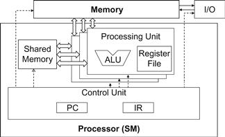
Control units in modern processors are quite complex, including sophisticated logic for fetching instructions and access ports to the instruction memory. They include on-chip instruction caches to reduce the latency of instruction fetch. Having multiple processing units share a control unit can result in significant reduction in hardware manufacturing cost and power consumption.
As the processors are increasingly power-limited, new processors will likely use SIMD designs. In fact, we may see even more processing units sharing a control unit in the future.
Conceptually, one should assume that threads in a block can execute in any order with respect to each other. Barrier synchronizations should be used whenever we want to ensure all threads have completed a common phase of their execution before any of them start the next phase. The correctness of executing a kernel should not depend on the fact that certain threads will execute in synchrony with each other. Having said this, we also want to point out that due to various hardware cost considerations, current CUDA devices actually bundle multiple threads for execution. Such an implementation strategy leads to performance limitations for certain types of kernel function code constructs. It is advantageous for application developers to change these types of constructs to other equivalent forms that perform better.
As we discussed in Chapter 4, current CUDA devices bundle several threads for execution. Each thread block is partitioned into warps. The execution of warps are implemented by an SIMD hardware (see “Warps and SIMD Hardware” sidebar). This implementation technique helps to reduce hardware manufacturing cost, lower runtime operation electricity cost, and enable some optimizations in servicing memory accesses. In the foreseeable future, we expect that warp partitioning will remain as a popular implementation technique. However, the size of a warp can easily vary from implementation to implementation. Up to this point in time, all CUDA devices have used similar warp configurations where each warp consists of 32 threads.
Thread blocks are partitioned into warps based on thread indices. If a thread block is organized into a 1D array (i.e., only threadIdx.x is used), the partition is straightforward; threadIdx.x values within a warp are consecutive and increasing. For a warp size of 32, warp 0 starts with thread 0 and ends with thread 31, warp 1 starts with thread 32 and ends with thread 63. In general, warp n starts with thread 32×n and ends with thread 32(n+1)−1. For a block of which the size is not a multiple of 32, the last warp will be padded with extra threads to fill up the 32 threads. For example, if a block has 48 threads, it will be partitioned into two warps, and its warp 1 will be padded with 16 extra threads.
For blocks that consist of multiple dimensions of threads, the dimensions will be projected into a linear order before partitioning into warps. The linear order is determined by placing the rows with larger y and z coordinates after those with lower ones. That is, if a block consists of two dimensions of threads, one would form the linear order by placing all threads of which threadIdx.y is 1 after those of which threadIdx.y is 0, threads of which threadIdx.y is 2 after those of which threadIdx.y is 1, and so on.
Figure 6.1 shows an example of placing threads of a 2D block into linear order. The upper part shows the 2D view of the block. Readers should recognize the similarity with the row-major layout of 2D arrays in C, as shown in Figure 4.3. Each thread is shown as Ty,x, x being threadIdx.x and y being threadIdx.y. The lower part of Figure 6.1 shows the linear view of the block. The first four threads are those threads of which the threadIdx.y value is 0; they are ordered with increasing threadIdx.x values. The next four threads are those threads of which the threadIdx.y value is 1; they are also placed with increasing threadIdx.x values. For this example, all 16 threads form half a warp. The warp will be padded with another 16 threads to complete a 32-thread warp. Imagine a 2D block with 8×8 threads. The 64 threads will form two warps. The first warp starts from T0,0 and ends with T3,7. The second warp starts with T4,0 and ends with T7,7. It would be a useful exercise to draw out the picture as an exercise.
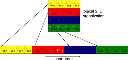
Figure 6.1 Placing 2D threads into linear order.
For a 3D block, we first place all threads of which the threadIdx.z value is 0 into the linear order. Among these threads, they are treated as a 2D block as shown in Figure 6.1. All threads of which the threadIdx.z value is 1 will then be placed into the linear order, and so on. For a 3D thread block of dimensions 2×8×4 (four in the x dimension, eight in the y dimension, and two in the z dimension), the 64 threads will be partitioned into two warps, with T0,0,0 through T0,7,3 in the first warp and T1,0,0 through T1,7,3 in the second warp.
The SIMD hardware executes all threads of a warp as a bundle. An instruction is run for all threads in the same warp. It works well when all threads within a warp follow the same execution path, or more formally referred to as control flow, when working their data. For example, for an if-else construct, the execution works well when either all threads execute the if part or all execute the else part. When threads within a warp take different control flow paths, the SIMD hardware will take multiple passes through these divergent paths. One pass executes those threads that follow the if part and another pass executes those that follow the else part. During each pass, the threads that follow the other path are not allowed to take effect. These passes are sequential to each other, thus they will add to the execution time.
The multipass approach to divergent warp execution extends the SIMD hardware’s ability to implement the full semantics of CUDA threads. While the hardware executes the same instruction for all threads in a warp, it selectively lets the threads take effect in each pass only, allowing every thread to take its own control flow path. This preserves the independence of threads while taking advantage of the reduced cost of SIMD hardware.
When threads in the same warp follow different paths of control flow, we say that these threads diverge in their execution. In the if-else example, divergence arises if some threads in a warp take the then path and some the else path. The cost of divergence is the extra pass the hardware needs to take to allow the threads in a warp to make their own decisions. Divergence also can arise in other constructs; for example, if threads in a warp execute a for loop that can iterate six, seven, or eight times for different threads. All threads will finish the first six iterations together. Two passes will be used to execute the seventh iteration, one for those that take the iteration and one for those that do not. Two passes will be used to execute the eighth iteration, one for those that take the iteration and one for those that do not.
In terms of source statements, a control construct can result in thread divergence when its decision condition is based on threadIdx values. For example, the statement if (threadIdx.x > 2) {} causes the threads to follow two divergent control flow paths. Threads 0, 1, and 2 follow a different path than threads 3, 4, 5, etc. Similarly, a loop can cause thread divergence if its loop condition is based on thread index values. Such usages arise naturally in some important parallel algorithms. We will use a reduction algorithm to illustrate this point.
A reduction algorithm derives a single value from an array of values. The single value could be the sum, the maximal value, the minimal value, etc. among all elements. All these types of reductions share the same computation structure. A reduction can be easily done by sequentially going through every element of the array. When an element is visited, the action to take depends on the type of reduction being performed. For a sum reduction, the value of the element being visited at the current step, or the current value, is added to a running sum. For a maximal reduction, the current value is compared to a running maximal value of all the elements visited so far. If the current value is larger than the running maximal, the current element value becomes the running maximal value. For a minimal reduction, the value of the element currently being visited is compared to a running minimal. If the current value is smaller than the running minimal, the current element value becomes the running minimal. The sequential algorithm ends when all the elements are visited. The sequential reduction algorithm is work-efficient in that every element is only visited once and only a minimal amount of work is performed when each element is visited. Its execution time is proportional to the number of elements involved. That is, the computational complexity of the algorithm is O(N), where N is the number of elements involved in the reduction.
The time needed to visit all elements of a large array motivates parallel execution. A parallel reduction algorithm typically resembles the structure of a soccer tournament. In fact, the elimination process of the World Cup is a reduction of “maximal” where the maximal is defined as the team that “beats” all other teams. The tournament “reduction” is done by multiple rounds. The teams are divided into pairs. During the first round, all pairs play in parallel. Winners of the first round advance to the second round, the winners of which advance to the third round, etc. With 16 teams entering a tournament, 8 winners will emerge from the first round, 4 from the second round, 2 from the third round, and 1 final winner from the fourth round. It should be easy to see that even with 1,024 teams, it takes only 10 rounds to determine the final winner. The trick is to have enough soccer fields to hold the 512 games in parallel during the first round, 256 games in the second round, 128 games in the third round, and so on. With enough fields, even with 60,000 teams, we can determine the final winner in just 16 rounds. Of course, one would need to have enough soccer fields and enough officials to accommodate the 30,000 games in the first round, etc.
Figure 6.2 shows a kernel function that performs parallel sum reduction. The original array is in the global memory. Each thread block reduces a section of the array by loading the elements of the section into the shared memory and performing parallel reduction. The code that loads the elements from global memory into the shared memory is omitted from Figure 6.2 for brevity. The reduction is done in place, which means the elements in the shared memory will be replaced by partial sums. Each iteration of the while loop in the kernel function implements a round of reduction. The __syncthreads() statement (line 5) in the while loop ensures that all partial sums for the previous iteration have been generated and thus all threads are ready to enter the current iteration before any one of them is allowed to do so. This way, all threads that enter the second iteration will be using the values produced in the first iteration. After the first round, the even elements will be replaced by the partial sums generated in the first round. After the second round, the elements of which the indices are multiples of four will be replaced with the partial sums. After the final round, the total sum of the entire section will be in element 0.
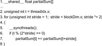
Figure 6.2 A simple sum reduction kernel.
In Figure 6.2, line 3 initializes the stride variable to 1. During the first iteration, the if statement in line 6 is used to select only the even threads to perform addition between two neighboring elements. The execution of the kernel is illustrated in Figure 6.3. The threads and the array element values are shown in the horizontal direction. The iterations taken by the threads are shown in the vertical direction with time progressing from top to bottom. Each row of Figure 6.3 shows the contents of the array elements after an iteration of the for loop.
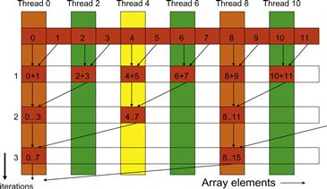
Figure 6.3 Execution of the sum reduction kernel.
As shown in Figure 6.3, the even elements of the array hold the pairwise partial sums after iteration 1. Before the second iteration, the value of the stride variable is doubled to 2. During the second iteration, only those threads of which the indices are multiples of four will execute the add statement in line 8. Each thread generates a partial sum that includes four elements, as shown in row 2. With 512 elements in each section, the kernel function will generate the sum of the entire section after nine iterations. By using blockDim.x as the loop bound in line 4, the kernel assumes that it is launched with the same number of threads as the number of elements in the section. That is, for a section size of 512, the kernel needs to be launched with 512 threads.1
Let’s analyze the total amount of work done by the kernel. Assume that the total number of elements to be reduced is N. The first round requires N/2 additions. The second round requires N/4 additions. The final round has only one addition. There are log2(N) rounds. The total number of additions performed by the kernel is N/2+N/4+N/8+…+1=N−1. Therefore, the computational complexity of the reduction algorithm is O(N). The algorithm is work-efficient. However, we also need to make sure that the hardware is efficiently utilized while executing the kernel.
The kernel in Figure 6.2 clearly has thread divergence. During the first iteration of the loop, only those threads of which the threadIdx.x are even will execute the add statement. One pass will be needed to execute these threads and one additional pass will be needed to execute those that do not execute line 8. In each successive iteration, fewer threads will execute line 8 but two passes will be still needed to execute all the threads during each iteration. This divergence can be reduced with a slight change to the algorithm.
Figure 6.4 shows a modified kernel with a slightly different algorithm for sum reduction. Instead of adding neighbor elements in the first round, it adds elements that are half a section away from each other. It does so by initializing the stride to be half the size of the section. All pairs added during the first round are half the section size away from each other. After the first iteration, all the pairwise sums are stored in the first half of the array. The loop divides the stride by 2 before entering the next iteration. Thus, for the second iteration, the stride variable value is one-quarter of the section size—that is, the threads add elements that are one-quarter a section away from each other during the second iteration.
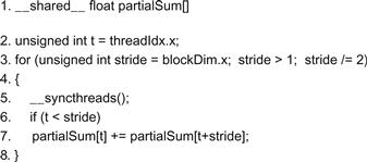
Figure 6.4 A kernel with fewer thread divergence.
Note that the kernel in Figure 6.4 still has an if statement (line 6) in the loop. The number of threads that execute line 7 in each iteration is the same as in Figure 6.2. So, why should there be a performance difference between the two kernels? The answer lies in the positions of threads that execute line 7 relative to those that do not.
Figure 6.5 illustrates the execution of the revised kernel. During the first iteration, all threads of which the threadIdx.x values are less than half of the size of the section execute line 7. For a section of 512 elements, threads 0–255 execute the add statement during the first iteration while threads 256–511 do not. The pairwise sums are stored in elements 0–255 after the first iteration. Since the warps consist of 32 threads with consecutive threadIdx.x values, all threads in warps 0–7 execute the add statement, whereas warps 8–15 all skip the add statement. Since all threads in each warp take the same path, there is no thread divergence!
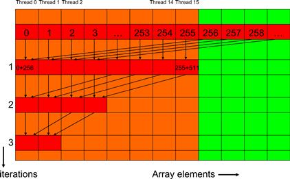
Figure 6.5 Execution of the revised algorithm.
The kernel in Figure 6.4 does not completely eliminate the divergence due to the if statement. Readers should verify that starting with the fifth iteration, the number of threads that execute line 7 will fall below 32. That is, the final five iterations will have only 16, 8, 4, 2, and 1 thread(s) performing the addition. This means that the kernel execution will still have divergence in these iterations. However, the number of iterations of the loop that has divergence is reduced from 10 to 5.
6.2 Global Memory Bandwidth
One of the most important factors of CUDA kernel performance is accessing data in the global memory. CUDA applications exploit massive data parallelism. Naturally, CUDA applications tend to process a massive amount of data from the global memory within a short period of time. In Chapter 5, we discussed tiling techniques that utilize shared memories to reduce the total amount of data that must be accessed by a collection of threads in the thread block. In this chapter, we will further discuss memory coalescing techniques that can more effectively move data from the global memory into shared memories and registers. Memory coalescing techniques are often used in conjunction with tiling techniques to allow CUDA devices to reach their performance potential by more efficiently utilizing the global memory bandwidth.2
The global memory of a CUDA device is implemented with DRAMs. Data bits are stored in DRAM cells that are small capacitors, where the presence or absence of a tiny amount of electrical charge distinguishes between 0 and 1. Reading data from a DRAM cell requires the small capacitor to use its tiny electrical charge to drive a highly capacitive line leading to a sensor and set off its detection mechanism that determines whether a sufficient amount of charge is present in the capacitor to qualify as a “1” (see “Why Are DRAMs So Slow?” sidebar). This process takes tens of nanoseconds in modern DRAM chips. Because this is a very slow process relative to the desired data access speed (sub-nanosecond access per byte), modern DRAMs use parallelism to increase their rate of data access.
Each time a DRAM location is accessed, many consecutive locations that include the requested location are actually accessed. Many sensors are provided in each DRAM chip and they work in parallel. Each senses the content of a bit within these consecutive locations. Once detected by the sensors, the data from all these consecutive locations can be transferred at very high speed to the processor. If an application can make focused use of data from consecutive locations, the DRAMs can supply the data at a much higher rate than if a truly random sequence of locations were accessed.
Why Are DRAMs So Slow?
The following figure shows a DRAM cell and the path for accessing its content. The decoder is an electronic circuit that uses a transistor to drive a line connected to the outlet gates of thousands of cells. It can take a long time for the line to be fully charged or discharged to the desired level.
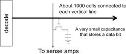
A more formidable challenge is for the cell to drive the line to the sense amplifiers and allow the sense amplifier to detect its content. This is based on electrical charge sharing. The gate lets out the tiny amount of electrical charge stored in the cell. If the cell content is “1,” the tiny amount of charge must raise the potential of the large capacitance formed by the long bit line and the input of the sense amplifier. A good analogy would be for someone to hold a small cup of coffee at one end of a long hallway for another person to smell the aroma propagated through the hallway to determine the flavor of the coffee.
One could speed up the process by using a larger, stronger capacitor in each cell. However, the DRAMs have been going in the opposite direction. The capacitors in each cell have been steadily reduced in size over time so that more bits can be stored in each chip. This is why the access latency of DRAMS has not decreased over time.
Recognizing the organization of modern DRAMs, current CUDA devices employ a technique that allows the programmers to achieve high global memory access efficiency by organizing memory accesses of threads into favorable patterns. This technique takes advantage of the fact that threads in a warp execute the same instruction at any given point in time. When all threads in a warp execute a load instruction, the hardware detects whether they access consecutive global memory locations. That is, the most favorable access pattern is achieved when all threads in a warp access consecutive global memory locations. In this case, the hardware combines, or coalesces, all these accesses into a consolidated access to consecutive DRAM locations. For example, for a given load instruction of a warp, if thread 0 accesses global memory location N,3 thread 1 location N+1, thread 2 location N+2, and so on, all these accesses will be coalesced, or combined into a single request for consecutive locations when accessing the DRAMs. Such coalesced access allows the DRAMs to deliver data at a rate close to the peak global memory bandwidth.
To understand how to effectively use coalescing hardware, we need to review how the memory addresses are formed in accessing C multidimensional array elements. As we showed in Chapter 4 (Figure 4.3, replicated as Figure 6.6 for convenience), multidimensional array elements in C and CUDA are placed into the linearly addressed memory space according to the row-major convention. That is, the elements of row 0 of a matrix are first placed in order into consecutive locations. They are followed by the elements of row 1 of the matrix, and so on. In other words, all elements in a row are placed into consecutive locations and entire rows are placed one after another. The term row major refers to the fact that the placement of data preserves the structure of rows: all adjacent elements in a row are placed into consecutive locations in the address space. Figure 6.6 shows a small example where the 16 elements of a 4×4 matrix M are placed into linearly addressed locations. The four elements of row 0 are first placed in their order of appearance in the row. Elements in row 1 are then placed, followed by elements of row 2, followed by elements of row 3. It should be clear that M0,0 and M1,0, though they appear to be consecutive in the 2D matrix, are placed four locations away in the linearly addressed memory.
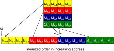
Figure 6.6 Placing matrix elements into linear order.
Figure 6.7 illustrates the favorable versus unfavorable CUDA kernel 2D row-major array data access patterns for memory coalescing. Recall from Figure 4.7 that in our simple matrix–matrix multiplication kernel, each thread accesses a row of the d_M array and a column of the d_N array. Readers should review Section 4.3 before continuing. Figure 6.7(a) illustrates the data access pattern of the d_M array, where threads in a warp read adjacent rows. That is, during iteration 0, threads in a warp read element 0 of rows 0–31. During iteration 1, these same threads read element 1 of rows 0–31. None of the accesses will be coalesced. A more favorable access pattern is shown in Figure 6.7(b), where each thread reads a column of d_N. During iteration 0, threads in warp 0 read element 1 of columns 0–31. All these accesses will be coalesced.
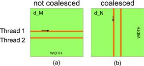
Figure 6.7 Memory access patterns in C 2D arrays for coalescing.
To understand why the pattern in Figure 6.7(b) is more favorable than that in Figure 6.7(a), we need to review how these matrix elements are accessed in more detail. Figure 6.8 shows a small example of the favorable access pattern in accessing a 4×4 matrix. The arrow in the top portion of Figure 6.8 shows the access pattern of the kernel code for one thread. This access pattern is generated by the access to d_N in Figure 4.7:
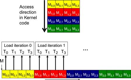
Figure 6.8 A coalesced access pattern.
Within a given iteration of the k loop, the k∗Width value is the same across all threads. Recall that Col = blockIdx.x∗blockDim.x + threadIdx.x. Since the value of blockIndx.x and blockDim.x are of the same value for all threads in the same block, the only part of k∗Width+Col that varies across a thread block is threadIdx.x. For example, in Figure 6.8, assume that we are using 4×4 blocks and that the warp size is 4. That is, for this toy example, we are using only one block to calculate the entire P matrix. The values of Width, blockDim.x, and blockIdx.x are 4, 4, and 0, respectively, for all threads in the block. In iteration 0, the k value is 0. The index used by each thread for accessing d_N is
d_N[k∗Width+Col]=d_N[k∗Width+blockIdx.x∗blockDim.x+threadIdx.x]
= d_N[0∗4 + 0∗4 + threadidx.x]
= d_N[threadIdx.x]
That is, the index for accessing d_N is simply the value of threadIdx.x. The d_N elements accessed by T0, T1, T2, and T3 are d_N[0], d_N[1], d_N[2], and d_N[3], respectively. This is illustrated with the “Load iteration 0” box of Figure 6.8. These elements are in consecutive locations in the global memory. The hardware detects that these accesses are made by threads in a warp and to consecutive locations in the global memory. It coalesces these accesses into a consolidated access. This allows the DRAMs to supply data at a high rate.
During the next iteration, the k value is 1. The index used by each thread for accessing d_N becomes
d_N[k∗Width+Col]=d_N[k∗Width+blockIdx.x∗blockDim.x+threadIdx.x]
= d_N[1∗4 + 0∗4 + threadidx.x]
= d_N[4+threadIdx.x]
The d_N elements accessed by T0, T1, T2, and T3 are d_N[5], d_N[6], d_N[7], and d_N[8], respectively, as shown with the “Load iteration 1” box in Figure 6.8. All these accesses are again coalesced into a consolidated access for improved DRAM bandwidth utilization.
Figure 6.9 shows an example of a matrix data access pattern that is not coalesced. The arrow in the top portion of the figure shows that the kernel code for each thread accesses elements of a row in sequence. The arrow in the top portion of Figure 6.9 shows the access pattern of the kernel code for one thread. This access pattern is generated by the access to d_M in Figure 4.7:
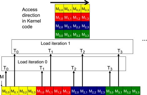
Figure 6.9 An uncoalesced access pattern.
d_M[Row∗Width + k]
Within a given iteration of the k loop, the k∗Width value is the same across all threads. Recall that Row = blockIdx.y∗blockDim.y + threadIdx.y. Since the value of blockIndx.y and blockDim.y are of the same value for all threads in the same block, the only part of Row∗Width+k that can vary across a thread block is threadIdx.y. In Figure 6.9, assume again that we are using 4×4 blocks and that the warp size is 4. The values of Width, blockDim.y, and blockIdx.y are 4, 4, and 0, respectively, for all threads in the block. In iteration 0, the k value is 0. The index used by each thread for accessing d_N is
d_M[Row∗Width+k] = d_M[(blockIdx.y∗blockDim.y+threadIdx.y)∗Width+k]
= d_M[((0∗4+threadIdx.y)∗4 + 0]
= d_M[threadIdx.x∗4]
That is, the index for accessing d_M is simply the value of threadIdx.x∗4. The d_M elements accessed by T0, T1, T2, and T3 are d_M[0], d_M[4], d_M[8], and d_M[12]. This is illustrated with the “Load iteration 0” box of Figure 6.9. These elements are not in consecutive locations in the global memory. The hardware cannot coalesce these accesses into a consolidated access.
During the next iteration, the k value is 1. The index used by each thread for accessing d_M becomes
d_M[Row∗Width+k] = d_M[(blockIdx.y∗blockDim.y+threadIdx.y)∗Width+k]
= d_M[(0∗4+threadidx.x)∗4+1]
= d_M[threadIdx.x∗4+1]
The d_M elements accessed by T0, T1, T2, T3 are d_M[1], d_M[5], d_M[9], and d_M[13], respectively, as shown with the “Load iteration 1” box in Figure 6.9. All these accesses again cannot be coalesced into a consolidated access.
For a realistic matrix, there are typically hundreds or even thousands of elements in each dimension. The elements accessed in each iteration by neighboring threads can be hundreds or even thousands of elements apart. The “Load iteration 0” box in the bottom portion shows how the threads access these nonconsecutive locations in the 0 iteration. The hardware will determine that accesses to these elements are far away from each other and cannot be coalesced. As a result, when a kernel loop iterates through a row, the accesses to global memory are much less efficient than the case where a kernel iterates through a column.
If an algorithm intrinsically requires a kernel code to iterate through data along the row direction, one can use the shared memory to enable memory coalescing. The technique is illustrated in Figure 6.10 for matrix multiplication. Each thread reads a row from d_M, a pattern that cannot be coalesced. Fortunately, a tiled algorithm can be used to enable coalescing. As we discussed in Chapter 5, threads of a block can first cooperatively load the tiles into the shared memory. Care must be taken to ensure that these tiles are loaded in a coalesced pattern. Once the data is in shared memory, it can be accessed either on a row basis or a column basis with much less performance variation because the shared memories are implemented as intrinsically high-speed, on-chip memory that does not require coalescing to achieve a high data access rate.
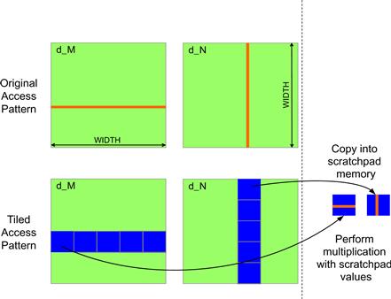
Figure 6.10 Using shared memory to enable coalescing.
We replicate Figure 5.7 here as Figure 6.11, where the matrix multiplication kernel loads two tiles of matrix d_M and d_N into the shared memory. Note that each thread in a thread block is responsible for loading one d_M element and one d_N element into Mds and Nds in each phase as defined by the for loop in line 8. Recall that there are TILE_WIDTH2 threads involved in each tile. The threads use threadIdx.y and threadIdx.y to determine the element of each matrix to load.
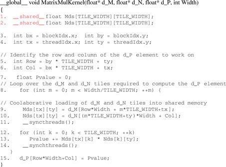
Figure 6.11 Tiled matrix multiplication kernel using shared memory.
The d_M elements are loaded in line 9, where the index calculation for each thread uses m to locate the left end of the tile. Each row of the tile is then loaded by TILE_WIDTH threads of which the threadIdx differ in the x dimension. Since these threads have consecutive threadIdx.x values, they are in the same warp. Also, the index calculation d_M[row][m∗TILE_SIZE+tx] makes these threads access elements in the same row. The question is whether adjacent threads in the warp indeed access adjacent elements in the row. Recall that elements in the same row are placed into consecutive locations of the global memory. Since the column index m∗TILE_SIZE+tx is such that all threads with adjacent tx values will access adjacent row elements, the answer is yes. The hardware detects that these threads in the same warp access consecutive locations in the global memory and combines them into a coalesced access.
In the case of d_N, the row index m∗TILE_SIZE+ty has the same value for all threads in the same warp; they all have the same ty value. Thus, threads in the same warp access the same row. The question is whether the adjacent threads in a warp access adjacent elements of a row. Note that the column index calculation for each thread Col is based on bx∗TILE_SIZE+tx (see line 4). Therefore, adjacent threads in a warp access adjacent elements in a row. The hardware detects that these threads in the same warp access consecutive locations in the global memory and combine them into a coalesced access.
Readers shall find it useful to draw a picture based on the kernel code in Figure 6.11 and identify the threadIdx.y and threadIdx.x values of the thread that loads each element of the tile. Lines 5, 6, 9, and 10 in Figure 6.11 form a frequently used programming pattern for loading matrix elements into shared memory in tiled algorithms. We would also like to encourage readers to analyze the data access pattern by the dot-product loop in lines 12 and 13. Note that the threads in a warp do not access consecutive location of Mds. This is not a problem since Mds is in shared memory, which does not require coalescing to achieve high-speed data access.
6.3 Dynamic Partitioning of Execution Resources
The execution resources in a streaming multiprocessor (SM) include registers, shared memory, thread block slots, and thread slots. These resources are dynamically partitioned and assigned to threads to support their execution. In Chapter 4, we have seen that the current generation of devices have 1,536 thread slots, each of which can accommodate one thread. These thread slots are partitioned and assigned to thread blocks during runtime. If each thread block consists of 512 threads, the 1,536 thread slots are partitioned and assigned to three blocks. In this case, each SM can accommodate up to three thread blocks due to limitations on thread slots. If each thread block contains 128 threads, the 1,536 thread slots are partitioned and assigned to 12 thread blocks. The ability to dynamically partition the thread slots among thread blocks makes SMs versatile. They can either execute many thread blocks each having few threads, or execute few thread blocks each having many threads. This is in contrast to a fixed partitioning method where each block receives a fixed amount of resources regardless of their real needs. Fixed partitioning results in wasted thread slots when a block has few threads and fails to support blocks that require more thread slots than the fixed partition allows.
Dynamic partitioning of resources can lead to subtle interactions between resource limitations, which can cause underutilization of resources. Such interactions can occur between block slots and thread slots. For example, if each block has 128 threads, the 1,536 thread slots can be partitioned and assigned to 12 blocks. However, since there are only 8 block slots in each SM, only 8 blocks will be allowed. This means that only 1,024 of the thread slots will be utilized. Therefore, to fully utilize both the block slots and thread slots, one needs at least 256 threads in each block.
As we mentioned in Chapter 4, the automatic variables declared in a CUDA kernel are placed into registers. Some kernels may use lots of automatic variables and others may use few of them. Thus, one should expect that some kernels require many registers and some require fewer. By dynamically partitioning the registers among blocks, the SM can accommodate more blocks if they require few registers and fewer blocks if they require more registers. One does, however, need to be aware of potential interactions between register limitations and other resource limitations.
In the matrix multiplication example, assume that each SM has 16,384 registers and the kernel code uses 10 registers per thread. If we have 16×16 thread blocks, how many threads can run on each SM? We can answer this question by first calculating the number of registers needed for each block, which is 10×16×16=2,560. The number of registers required by six blocks is 15,360, which is under the 16,384 limit. Adding another block would require 17,920 registers, which exceeds the limit. Therefore, the register limitation allows blocks that altogether have 1,536 threads to run on each SM, which also fits within the limit of block slots and 1,536 thread slots.
Now assume that the programmer declares another two automatic variables in the kernel and bumps the number of registers used by each thread to 12. Assuming the same 16×16 blocks, each block now requires 12×16×16=3,072 registers. The number of registers required by six blocks is now 18,432, which exceeds the register limitation. The CUDA runtime system deals with this situation by reducing the number of blocks assigned to each SM by one, thus reducing the number of registered required to 15,360. This, however, reduces the number of threads running on an SM from 1,536 to 1,280. That is, by using two extra automatic variables, the program saw a one-sixth reduction in the warp parallelism in each SM. This is sometimes a referred to as a “performance cliff” where a slight increase in resource usage can result in significant reduction in parallelism and performance achieved [RRS2008]. Readers are referred to the CUDA Occupancy Calculator [NVIDIA], which is a downloadable Excel sheet that calculates the actual number of threads running on each SM for a particular device implementation given the usage of resources by a kernel.
6.4 Instruction Mix and Thread Granularity
An important algorithmic decision in performance tuning is the granularity of threads. It is often advantageous to put more work into each thread and use fewer threads. Such advantage arises when some redundant work exists between threads. In the current generation of devices, each SM has limited instruction processing bandwidth. Every instruction consumes instruction processing bandwidth, whether it is a floating-point calculation instruction, a load instruction, or a branch instruction. Eliminating redundant instructions can ease the pressure on the instruction processing bandwidth and improve the overall execution speed of the kernel.
Figure 6.12 illustrates such an opportunity in matrix multiplication. The tiled algorithm in Figure 6.11 uses one thread to compute one element of the output d_P matrix. This requires a dot product between one row of d_M and one column of d_N.
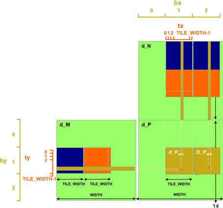
Figure 6.12 Increased thread granularity with rectangular tiles.
The opportunity of thread granularity adjustment comes from the fact that multiple blocks redundantly load each d_M tile. As shown in Figure 6.12, the calculation of two d_P elements in adjacent tiles uses the same d_M row. With the original tiled algorithm, the same d_M row is redundantly loaded by the two blocks assigned to generate these two Pd tiles. One can eliminate this redundancy by merging the two thread blocks into one. Each thread in the new thread block now calculates two d_P elements. This is done by revising the kernel so that two dot products are computed by the innermost loop of the kernel. Both dot products use the same Mds row but different Nds columns. This reduces the global memory access by one-quarter. Readers are encouraged to write the new kernel as an exercise.
The potential downside is that the new kernel now uses even more registers and shared memory. As we discussed in the previous section, the number of blocks that can be running on each SM may decrease. It also reduces the total number of thread blocks by half, which may result in an insufficient amount of parallelism for matrices of smaller dimensions. In practice, we found that combining up to four adjacent horizontal blocks to compute adjacent horizontal tiles improves the performance of large (2,048×2,048 or more) matrix multiplication.
6.5 Summary
In this chapter, we reviewed the major aspects of CUDA C application performance on a CUDA device: control flow divergence, global memory coalescing, dynamic resource partitioning, and instruction mixes. We presented practical techniques for creating good program patterns for these performance aspects. We will continue to study practical applications of these techniques in the case studies in the next few chapters.
6.6 Exercises
6.1 The kernels in Figures 6.2 and 6.4 are wasteful in their use of threads; half of the threads in each block never execute. Modify the kernels to eliminate such waste. Give the relevant execute configuration parameter values at the kernel launch. Is there a cost in terms of an extra arithmetic operation needed? Which resource limitation can be potentially addressed with such modification? (Hint: line 2 and/or line 4 can be adjusted in each case; the number of elements in the section may increase.)
6.2 Compare the modified kernels you wrote for Exercise 6.1. Which modification introduced fewer additional arithmetic operations?
6.3 Write a complete kernel based on Exercise 6.1 by (1) adding the statements that load a section of the input array from global memory to shared memory, (2) using blockIdx.x to allow multiple blocks to work on different sections of the input array, and (3) writing the reduction value for the section to a location according to the blockIdx.x so that all blocks will deposit their section reduction value to the lower part of the input array in global memory.
6.4 Design a reduction program based on the kernel you wrote for Exercise 6.3. The host code should (1) transfer a large input array to the global memory, and (2) use a loop to repeatedly invoke the kernel you wrote for Exercise 6.3 with adjusted execution configuration parameter values so that the reduction result for the input array will eventually be produced.
6.5 For the matrix multiplication kernel in Figure 6.11, draw the access patterns of threads in a warp of lines 9 and 10 for a small 16×16 matrix size. Calculate the tx and ty values for each thread in a warp and use these values in the d_M and d_N index calculations in lines 9 and 10. Show that the threads indeed access consecutive d_M and d_N locations in global memory during each iteration.
6.6 For the simple matrix–matrix multiplication (M –× N) based on row-major layout, which input matrix will have coalesced accesses?
6.7 For the tiled matrix–matrix multiplication (M × N) based on row-major layout, which input matrix will have coalesced accesses?
6.8 For the simple reduction kernel, if the block size is 1,024 and warp size is 32, how many warps in a block will have divergence during the fifth iteration?
6.9 For the improved reduction kernel, if the block size is 1,024 and warp size is 32, how many warps will have divergence during the fifth iteration?
6.10 Write a matrix multiplication kernel function that corresponds to the design illustrated in Figure 6.12.
6.11 The following scalar product code tests your understanding of the basic CUDA model. The following code computes 1,024 dot products, each of which is calculated from a pair of 256-element vectors. Assume that the code is executed on G80. Use the code to answer the following questions.
1 #define VECTOR_N 1024
2 #define ELEMENT_N 256
3 const int DATA_N = VECTOR_N ∗ ELEMENT_N;
4 const int DATA_SZ = DATA_N ∗ sizeof(float);
5 const int RESULT_SZ = VECTOR_N ∗ sizeof(float);
…
6 float ∗d_A, ∗d_B, ∗d_C;
…
7 cudaMalloc((void ∗∗)&d_A, DATA_SZ);
8 cudaMalloc((void ∗∗)&d_B, DATA_SZ);
9 cudaMalloc((void ∗∗)&d_C, RESULT_SZ);
…
10 scalarProd<<<VECTOR_N, ELEMENT_N>>>(d_C, d_A, d_B, ELEMENT_N);
11
12 __global__ void
13 scalarProd(float ∗d_C, float ∗d_A, float ∗d_B, int ElementN)
14 {
15 __shared__ float accumResult[ELEMENT_N];
16 //Current vectors bases
17 float ∗A = d_A + ElementN ∗ blockIdx.x;
18 float ∗B = d_B + ElementN ∗ blockIdx.x;
19 int tx = threadIdx.x;
20
21 accumResult[tx] = A[tx] ∗ B[tx];
22
23 for(int stride = ElementN /2; stride > 0; stride >>= 1)
24 {
25 __syncthreads();
26 if(tx < stride)
27 accumResult[tx] += accumResult[stride + tx];
28 }
30 d_C[blockIdx.x] = accumResult[0];
31 }
a. How many threads are there in total?
b. How many threads are there in a warp?
c. How many threads are there in a block?
d. How many global memory loads and stores are done for each thread?
e. How many accesses to shared memory are done for each block?
f. List the source code lines, if any, that cause shared memory bank conflicts.
g. How many iterations of the for loop (line 23) will have branch divergence? Show your derivation.
h. Identify an opportunity to significantly reduce the bandwidth requirement on the global memory. How would you achieve this? How many accesses can you eliminate?
6.12 In Exercise 4.2, out of the possible range of values for BLOCK_SIZE, for what values of BLOCK_SIZE will the kernel completely avoid uncoalesced accesses to global memory?
6.13 In an attempt to improve performance, a bright young engineer changed the CUDA code in Figure 6.4 into the following.
__shared__ float partialSum[];
unsigned int tid = threadIdx.x;
for (unsigned int stride = n>>1; stride >= 32; stride >>= 1) {
__syncthreads();
if (tid < stride)
shared[tid] += shared[tid + stride];
}
__syncthreads();
if (tid < 32) { // unroll last 5 predicated steps
shared[tid] += shared[tid + 16];
shared[tid] += shared[tid + 8];
shared[tid] += shared[tid + 4];
shared[tid] += shared[tid + 2];
shared[tid] += shared[tid + 1];
}
a. Do you believe that the performance will be improved? Why or why not?
References
1. CUDA Occupancy Calculator.
2. CUDA C. Best Practices Guide. 2012;v. 4.2.
3. Ryoo, S., Rodrigues, C., Stone, S., Baghsorkhi, S., Ueng, S., Stratton, J., & Hwu, W. Program optimization space pruning for a multithreaded GPU, Proceedings of the 6th ACM/IEEE International Symposium on Code Generation and Optimization, April 6–9, 2008.
4. Ryoo, S., Rodrigues, C. I., Baghsorkhi, S. S., Stone, S. S., Kirk, D. B., & Hwu, W. W. Optimization principles and application performance evaluation of a multithreaded GPU using CUDA, Proceedings of the 13th ACM SIGPLAN Symposium on Principles and Practice of Parallel Programming, February 2008.
1Note that using the same number of threads as the number of elements in a section is wasteful. Half of the threads in a block will never execute. Readers are encouraged to modify the kernel and the kernel launch execution configuration parameters to eliminate this waste (see Exercise 6.1).
2Recent CUDA devices use on-chip caches for global memory data. Such caches automatically coalesce more of the kernel access patterns and somewhat reduce the need for programmers to manually rearrange their access patterns. However, even with caches, coalescing techniques will continue to have a significant effect on kernel execution performance in the foreseeable future.
3Different CUDA devices may also impose alignment requirements on N. For example, in some CUDA devices, N is required to be aligned to 16-word boundaries. That is, the lower 6 bits of N should all be 0 bits. We will discuss techniques that address this alignment requirement in Chapter 12.