
Chapter 5
CUDA Memories
Chapter Outline
5.1 Importance of Memory Access Efficiency
5.2 CUDA Device Memory Types
5.3 A Strategy for Reducing Global Memory Traffic
5.4 A Tiled Matrix–Matrix Multiplication Kernel
5.5 Memory as a Limiting Factor to Parallelism
5.6 Summary
5.7 Exercises
So far, we have learned to write a CUDA kernel function that is executed by a massive number of threads. The data to be processed by these threads is first transferred from the host memory to the device global memory. The threads then access their portion of the data from the global memory using their block IDs and thread IDs. We have also learned more details of the assignment and scheduling of threads for execution. Although this is a very good start, these simple CUDA kernels will likely achieve only a small fraction of the potential speed of the underlying hardware. The poor performance is due to the fact that global memory, which is typically implemented with dynamic random access memory (DRAM), tends to have long access latencies (hundreds of clock cycles) and finite access bandwidth. While having many threads available for execution can theoretically tolerate long memory access latencies, one can easily run into a situation where traffic congestion in the global memory access paths prevents all but very few threads from making progress, thus rendering some of the streaming multiprocessors (SMs) idle. To circumvent such congestion, CUDA provides a number of additional methods for accessing memory that can remove the majority of data requests to the global memory. In this chapter, you will learn to use these memories to boost the execution efficiency of CUDA kernels.
5.1 Importance of Memory Access Efficiency
We can illustrate the effect of memory access efficiency by calculating the expected performance level of the matrix multiplication kernel code in Figure 4.7, replicated in Figure 5.1. The most important part of the kernel in terms of execution time is the for loop that performs inner product calculation.
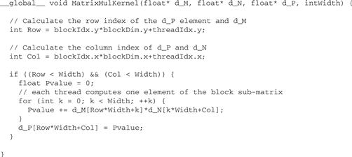
Figure 5.1 A simple matrix–matrix multiplication kernel using one thread to compute each d_P element (copied from Figure 4.7).
for (int k = 0; k < Width; ++k)
Pvalue += d_M[Row∗Width+k] ∗ d_N[k∗Width+Col];
In every iteration of this loop, two global memory accesses are performed for one floating-point multiplication and one floating-point addition. One global memory access fetches a d_M[] element and the other fetches a d_N[] element. One floating-point operation multiplies the d_M[] and d_N[] elements fetched and the other accumulates the product into Pvalue. Thus, the ratio of floating-point calculation to global memory access operation is 1:1, or 1.0. We will refer to this ratio as the compute to global memory access (CGMA) ratio, defined as the number of floating-point calculations performed for each access to the global memory within a region of a CUDA program.
CGMA has major implications on the performance of a CUDA kernel. In a high-end device today, the global memory bandwidth is around 200 GB/s. With 4 bytes in each single-precision floating-point value, one can expect to load no more than 50 (200/4) giga single-precision operands per second. With a CGMA ration of 1.0, the matrix multiplication kernel will execute no more than 50 giga floating-point operations per second (GFLOPS). While 50 GFLOPS is a respectable number, it is only a tiny fraction of the peak single-precision performance of 1,500 GFLOPS or higher for these high-end devices. We need to increase the CGMA ratio to achieve a higher level of performance for the kernel. For the matrix multiplication code to achieve the peak 1,500 GFLOPS rating of the processor, we need a CGMA value of 30. The desired CGMA ratio has roughly doubled in the past three generations of devices.
The von Neumann Model
In his seminal 1945 report, John von Neumann described a model for building electronic computers that is based on the design of the pioneering EDVAC computer. This model, now commonly referred to as the von Neumann model, has been the foundational blueprint for virtually all modern computers.
The von Neumann model is illustrated here. The computer has an I/O that allows both programs and data to be provided to and generated from the system. To execute a program, the computer first inputs the program and its data into the memory.
The program consists of a collection of instructions. The control unit maintains a program counter (PC), which contains the memory address of the next instruction to be executed. In each “instruction cycle,” the control unit uses the PC to fetch an instruction into the instruction register (IR). The instruction bits are then used to determine the action to be taken by all components of the computer. This is the reason why the model is also called the “stored program” model, which means that a user can change the actions of a computer by storing a different program into its memory.
5.2 CUDA Device Memory Types
CUDA supports several types of memory that can be used by programmers to achieve a high CGMA ratio and thus a high execution speed in their kernels. Figure 5.2 shows these CUDA device memories. At the bottom of the figure, we see global memory and constant memory. These types of memory can be written (W) and read (R) by the host by calling API functions.1 We have already introduced global memory in Chapter 3. The constant memory supports short-latency, high-bandwidth, read-only access by the device when all threads simultaneously access the same location.
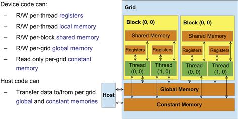
Figure 5.2 Overview of the CUDA device memory model.
Registers and shared memory in Figure 5.2 are on-chip memories. Variables that reside in these types of memory can be accessed at very high speed in a highly parallel manner. Registers are allocated to individual threads; each thread can only access its own registers. A kernel function typically uses registers to hold frequently accessed variables that are private to each thread. Shared memory is allocated to thread blocks; all threads in a block can access variables in the shared memory locations allocated to the block. Shared memory is an efficient means for threads to cooperate by sharing their input data and the intermediate results of their work. By declaring a CUDA variable in one of the CUDA memory types, a CUDA programmer dictates the visibility and access speed of the variable.
To fully appreciate the difference between registers, shared memory, and global memory, we need to go into a little more detail of how these different types of memories are realized and used in modern processors. The global memory in the CUDA programming model maps to the memory of the von Neumann model (see “The von Neumann Model” sidebar). The processor box in Figure 5.3 corresponds to the processor chip boundary that we typically see today. The global memory is off the processor chip and is implemented with DRAM technology, which implies long access latencies and relatively low access bandwidth. The registers correspond to the “register file” of the von Neumann model. It is on the processor chip, which implies very short access latency and drastically higher access bandwidth. In a typical device, the aggregated access bandwidth of the register files is about two orders of magnitude of that of the global memory. Furthermore, whenever a variable is stored in a register, its accesses no longer consume off-chip global memory bandwidth. This will be reflected as an increase in the CGMA ratio.
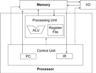
Figure 5.3 Memory versus registers in a modern computer based on the von Neumann model.
A more subtle point is that each access to registers involves fewer instructions than global memory. In Figure 5.3, the processor uses the PC value to fetch instructions from memory into the IR (see “The von Neumann Model” sidebar). The bits of the fetched instructions are then used to control the activities of the components of the computer. Using the instruction bits to control the activities of the computer is referred to as instruction execution. The number of instructions that can be fetched and executed in each clock cycle is limited. Therefore, the more instructions that need to be executed for a program, the more time it can take to execute the program.
Arithmetic instructions in most modern processors have “built-in” register operands. For example, a typical floating addition instruction is of the form
fadd r1, r2, r3
where r2 and r3 are the register numbers that specify the location in the register file where the input operand values can be found. The location for storing the floating-point addition result value is specified by r1. Therefore, when an operand of an arithmetic instruction is in a register, there is no additional instruction required to make the operand value available to the arithmetic and logic unit (ALU) where the arithmetic calculation is done.
On the other hand, if an operand value is in global memory, one needs to perform a memory load operation to make the operand value available to the ALU. For example, if the first operand of a floating-point addition instruction is in global memory of a typical computer today, the instructions involved will likely be
load r2, r4, offset
fadd r1, r2, r3
where the load instruction adds an offset value to the contents of r4 to form an address for the operand value. It then accesses the global memory and places the value into register r2. The fadd instruction then performs the floating addition using the values in r2 and r3 and places the result into r1. Since the processor can only fetch and execute a limited number of instructions per clock cycle, the version with an additional load will likely take more time to process than the one without. This is another reason why placing the operands in registers can improve execution speed.
Processing Units and Threads
Now that we have introduced the von Neumann model, we are ready to discuss how threads are implemented. A thread in modern computers is a virtualized von Neumann processor. Recall that a thread consists of the code of a program, the particular point in the code that is being executed, and the value of its variables and data structures.
In a computer based on the von Neumann model, the code of the program is stored in the memory. The PC keeps track of the particular point of the program that is being executed. The IR holds the instruction that is fetched from the point execution. The register and memory hold the values of the variables and data structures.
Modern processors are designed to allow context switching, where multiple threads can timeshare a processor by taking turns to make progress. By carefully saving and restoring the PC value and the contents of registers and memory, we can suspend the execution of a thread and correctly resume the execution of the thread later.
Some processors provide multiple processing units, which allow multiple threads to make simultaneous progress. Figure 5.4 shows a single instruction, multiple data (SIMD) design style where all processing units share a PC and IR. Under this design, all threads making simultaneous progress execute the same instruction in the program.
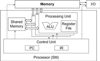
Figure 5.4 Shared memory versus registers in a CUDA device SM.
Finally, there is another subtle reason why placing an operand value in registers is preferable. In modern computers, the energy consumed for accessing a value from the register file is at least an order of magnitude lower than for accessing a value from the global memory. We will look at more details of the speed and energy difference in accessing these two hardware structures in modern computers soon. However, as we will soon learn, the number of registers available to each thread is quite limited in today’s GPUs. We need to be careful not to oversubscribe to this limited resource.
Figure 5.4 shows shared memory and registers in a CUDA device. Although both are on-chip memories, they differ significantly in functionality and cost of access. Shared memory is designed as part of the memory space that resides on the processor chip (see Section 4.2). When the processor accesses data that resides in the shared memory, it needs to perform a memory load operation, just like accessing data in the global memory. However, because shared memory resides on-chip, it can be accessed with much lower latency and much higher bandwidth than the global memory. Because of the need to perform a load operation, share memory has longer latency and lower bandwidth than registers. In computer architecture, share memory is a form of scratchpad memory.
One important difference between the share memory and registers in CUDA is that variables that reside in the shared memory are accessible by all threads in a block. This is in contrast to register data, which is private to a thread. That is, shared memory is designed to support efficient, high-bandwidth sharing of data among threads in a block. As shown in Figure 5.4, a CUDA device SM typically employs multiple processing units, referred to as SPs in Figure 4.14, to allow multiple threads to make simultaneous progress (see “Processing Units and Threads” sidebar). Threads in a block can be spread across these processing units. Therefore, the hardware implementations of shared memory in these CUDA devices are typically designed to allow multiple processing units to simultaneously access its contents to support efficient data sharing among threads in a block. We will be learning several important types of parallel algorithms that can greatly benefit from such efficient data sharing among threads.
It should be clear by now that registers, shared memory, and global memory all have different functionalities, latencies, and bandwidth. It is, therefore, important to understand how to declare a variable so that it will reside in the intended type of memory. Table 5.1 presents the CUDA syntax for declaring program variables into the various types of device memory. Each such declaration also gives its declared CUDA variable a scope and lifetime. Scope identifies the range of threads that can access the variable: by a single thread only, by all threads of a block, or by all threads of all grids. If a variable’s scope is a single thread, a private version of the variable will be created for every thread; each thread can only access its private version of the variable. For example, if a kernel declares a variable of which the scope is a thread and it is launched with one million threads, one million versions of the variable will be created so that each thread initializes and uses its own version of the variable.
Table 5.1 CUDA Variable Type Qualifiers
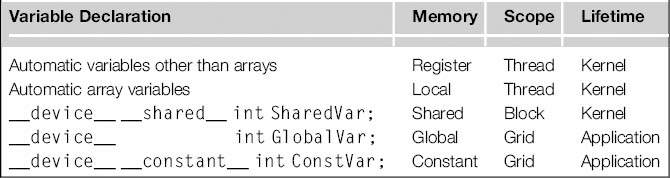
Lifetime tells the portion of the program’s execution duration when the variable is available for use: either within a kernel’s execution or throughout the entire application. If a variable’s lifetime is within a kernel’s execution, it must be declared within the kernel function body and will be available for use only by the kernel’s code. If the kernel is invoked several times, the value of the variable is not maintained across these invocations. Each invocation must initialize the variable to use them. On the other hand, if a variable’s lifetime is throughout the entire application, it must be declared outside of any function body. The contents of these variables are maintained throughout the execution of the application and available to all kernels.
As shown in Table 5.1, all automatic scalar variables declared in kernel and device functions are placed into registers. We refer to variables that are not arrays as scalar variables. The scopes of these automatic variables are within individual threads. When a kernel function declares an automatic variable, a private copy of that variable is generated for every thread that executes the kernel function. When a thread terminates, all its automatic variables also cease to exist. In Figure 5.1, variables Row, Col, and Pvalue are all automatic variables and fall into this category. Note that accessing these variables is extremely fast and parallel but one must be careful not to exceed the limited capacity of the register storage in the hardware implementations. We will address this point in Chapter 6.
Automatic array variables are not stored in registers.2 Instead, they are stored into the global memory and may incur long access delays and potential access congestions. The scope of these arrays is, like automatic scalar variables, limited to individual threads. That is, a private version of each automatic array is created for and used by every thread. Once a thread terminates its execution, the contents of its automatic array variables also cease to exist. From our experience, one seldom needs to use automatic array variables in kernel functions and device functions.
If a variable declaration is preceded by the keyword __shared__ (each __ consists of two _ characters), it declares a shared variable in CUDA. One can also add an optional __device__ in front of __shared__ in the declaration to achieve the same effect. Such declaration typically resides within a kernel function or a device function. Shared variables reside in shared memory. The scope of a shared variable is within a thread block, that is, all threads in a block see the same version of a shared variable. A private version of the shared variable is created for and used by each thread block during kernel execution. The lifetime of a shared variable is within the duration of the kernel. When a kernel terminates its execution, the contents of its shared variables cease to exist. As we discussed earlier, shared variables are an efficient means for threads within a block to collaborate with each other. Accessing shared variables from the shared memory is extremely fast and highly parallel. CUDA programmers often use shared variables to hold the portion of global memory data that are heavily used in an execution phase of a kernel. One may need to adjust the algorithms used to create execution phases that heavily focus on small portions of the global memory data, as we will demonstrate with matrix multiplication in Section 5.3.
If a variable declaration is preceded by the keyword __constant__ (each __ consists of two _ characters), it declares a constant variable in CUDA. One can also add an optional __device__ in front of __constant__ to achieve the same effect. Declaration of constant variables must be outside any function body. The scope of a constant variable is all grids, meaning that all threads in all grids see the same version of a constant variable. The lifetime of a constant variable is the entire application execution. Constant variables are often used for variables that provide input values to kernel functions. Constant variables are stored in the global memory but are cached for efficient access. With appropriate access patterns, accessing constant memory is extremely fast and parallel. Currently, the total size of constant variables in an application is limited at 65,536 bytes. One may need to break up the input data volume to fit within this limitation, as we will illustrate in Chapter 8.
A variable of which the declaration is preceded only by the keyword __device__ (each __ consists of two _ characters) is a global variable and will be placed in the global memory. Accesses to a global variable are slow. Latency and throughput of accessing global variables have been improved with caches in more recent devices. One important advantage of global variables is that they are visible to all threads of all kernels. Their contents also persist through the entire execution. Thus, global variables can be used as a means for threads to collaborate across blocks. One must, however, be aware of the fact that there is currently no easy way to synchronize between threads from different thread blocks or to ensure data consistency across threads when accessing global memory other than terminating the current kernel execution.3 Therefore, global variables are often used to pass information from one kernel invocation to another kernel invocation.
In CUDA, pointers are used to point to data objects in global memory. There are two typical ways in which pointer usage arises in kernel and device functions. First, if an object is allocated by a host function, the pointer to the object is initialized by cudaMalloc() and can be passed to the kernel function as a parameter. For example, the parameters d_M, d_N, and d_P in Figure 5.1 are such pointers. The second type of usage is to assign the address of a variable declared in the global memory to a pointer variable. For example, the statement {float∗ ptr = &GlobalVar;} in a kernel function assigns the address of GlobalVar into an automatic pointer variable ptr. Readers should refer to the CUDA Programming Guide for using pointers in other memory types.
5.3 A Strategy for Reducing Global Memory Traffic
We have an intrinsic trade-off in the use of device memories in CUDA: global memory is large but slow, whereas the shared memory is small but fast. A common strategy is partition the data into subsets called tiles so that each tile fits into the shared memory. The term tile draws on the analogy that a large wall (i.e., the global memory data) can be covered by tiles (i.e., subsets that each can fit into the shared memory). An important criterion is that the kernel computation on these tiles can be done independently of each other. Note that not all data structures can be partitioned into tiles given an arbitrary kernel function.
The concept of tiling can be illustrated with the matrix multiplication example. Figure 5.5 shows a small example of matrix multiplication. It corresponds to the kernel function in Figure 5.1. For brevity, we abbreviate d_P[y∗Width+x], d_M[y∗Width+x], and d_N[y∗Width+x] into Py,x, My,x, and Ny,x, respectively. This example assumes that we use four 2×2 blocks to compute the P matrix. Figure 5.5 highlights the computation done by the four threads of block(0,0). These four threads compute P0,0, P0,1, P1,0, and P1,1. The accesses to the M and N elements by thread(0,0) and thread(0,1) of block(0,0) are highlighted with black arrows. For example, thread(0,0) reads M0,0 and N0,0, followed by M0,1, and N1,0 followed by M0,2 and N2,0, followed by M0,3 and N3,0.
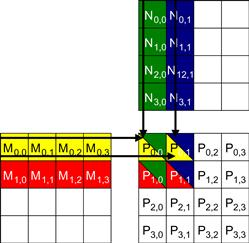
Figure 5.5 A small example of matrix multiplication. For brevity, We show d_M[y∗Width+x], d_N[y∗Width+x], d_P[y∗Width+x] as My,x, Ny,x, Py,x, respectively.
Figure 5.6 shows the global memory accesses done by all threads in block0,0. The threads are listed in the vertical direction, with time of access increasing to the right in the horizontal direction. Note that each thread accesses four elements of M and four elements of N during its execution. Among the four threads highlighted, there is a significant overlap in terms of the M and N elements they access. For example, thread0,0 and thread0,1 both access M0,0 as well as the rest of row 0 of M. Similarly, thread0,1 and thread1,1 both access N0,1 as well as the rest of column 1 of N.
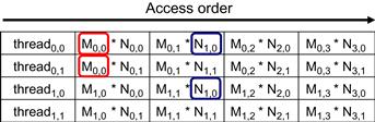
Figure 5.6 Global memory accesses performed by threads in block0,0.
The kernel in Figure 5.1 is written so that both thread0,0 and thread0,1 access row 0 elements of M from the global memory. If we can somehow manage to have thread0,0 and thread1,0 to collaborate so that these M elements are only loaded from global memory once, we can reduce the total number of accesses to the global memory by half. In general, we can see that every M and N element is accessed exactly twice during the execution of block0,0. Therefore, if we can have all four threads to collaborate in their accesses to global memory, we can reduce the traffic to the global memory by half.
Readers should verify that the potential reduction in global memory traffic in the matrix multiplication example is proportional to the dimension of the blocks used. With N×N blocks, the potential reduction of global memory traffic would be N. That is, if we use 16×16 blocks, one can potentially reduce the global memory traffic to 1/16 through collaboration between threads.
Traffic congestion obviously does not only arise in computing. Most of us have experienced traffic congestion in highway systems, as illustrated in Figure 5.7. The root cause of highway traffic congestion is that there are too many cars all squeezing through a road that is designed for a much smaller number of vehicles. When congestion occurs, the travel time for each vehicle is greatly increased. Commute time to work can easily double or triple during traffic congestion.
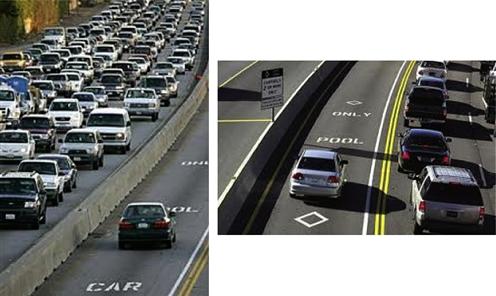
Figure 5.7 Reducing traffic congestion in highway systems.
All proposed solutions for reduced traffic congestion involve reduction of cars on the road. Assuming that the number of commuters is constant, people need to share rides to reduce the number of cars on the road. A common way to share rides in the United States is carpools, where a group of commuters take turns to drive the group to work in one vehicle. In some countries, the government simply disallows certain classes of cars to be on the road on a daily basis. For example, cars with odd license plates may not be allowed on the road on Monday, Wednesday, or Friday. This encourages people whose cars are allowed on different days to form a carpool group. There are also countries where the government makes gasoline so expensive that people form carpools to save money. In other countries, the government may provide incentives for behavior that reduces the number of cars on the road. In the United States, some lanes of congested highways are designated as carpool lanes—only cars with more than two or three people are allowed to use these lanes. All these measures for encouraging carpooling are designed to overcome the fact that carpooling requires extra effort, as we show in Figure 5.8.
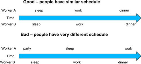
Figure 5.8 Carpooling requires synchronization among people.
The top half of Figure 5.8 shows a good schedule pattern for carpooling. Time goes from left to right. Worker A and worker B have similar schedules for sleep, work, and dinner. This allows these two workers to easily go to work and return home in one car. Their similar schedules allow them to more easily agree on a common departure time and return time. This is, however, not the case of the schedules shown in the bottom half of Figure 5.8. Worker A and worker B have very different habits in this case. Worker A parties until sunrise, sleeps during the day, and goes to work in the evening. Worker B sleeps at night, goes to work in the morning, and returns home for dinner at 6 p.m. The schedules are so wildly different that there is no way these two workers can coordinate a common time to drive to work and return home in one car. For these workers to form a carpool, they need to negotiate a common schedule similar to what is shown in the top half of Figure 5.8.
Tiled algorithms are very similar to carpooling arrangements. We can think of data values accessed by each thread as commuters and DRAM requested as vehicles. When the rate of DRAM requests exceeds the provisioned bandwidth of the DRAM system, traffic congestion arises and the arithmetic units become idle. If multiple threads access data from the same DRAM location, they can form a “carpool” and combine their accesses into one DRAM request. This, however, requires the threads to have a similar execution schedule so that their data accesses can be combined into one. This is shown in Figure 5.9, where the top portion shows two threads that access the same data elements with similar timing. The bottom half shows two threads that access their common data in very different times. The reason why the bottom half is a bad arrangement is that data elements brought back from the DRAM need to be kept in the on-chip memory for a long time, waiting for thread 2 to consume them. This will likely require a large number of data elements to be kept around, thus large on-chip memory requirements. As we will show in the next section, we will use barrier synchronization to keep the threads that form the “carpool” group to follow approximately the same execution timing.
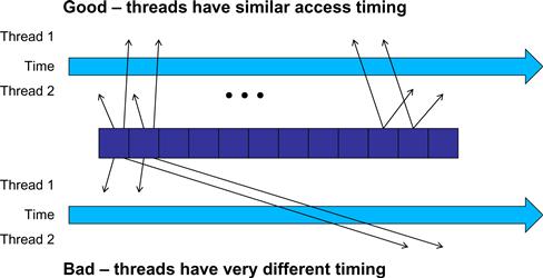
Figure 5.9 Tiled algorithms require synchronization among threads.
5.4 A Tiled Matrix–Matrix Multiplication Kernel
We now present an algorithm where threads collaborate to reduce the traffic to the global memory. The basic idea is to have the threads to collaboratively load M and N elements into the shared memory before they individually use these elements in their dot product calculation. Keep in mind that the size of the shared memory is quite small and one must be careful not to exceed the capacity of the shared memory when loading these M and N elements into the shared memory. This can be accomplished by dividing the M and N matrices into smaller tiles. The size of these tiles is chosen so that they can fit into the shared memory. In the simplest form, the tile dimensions equal those of the block, as illustrated in Figure 5.10.
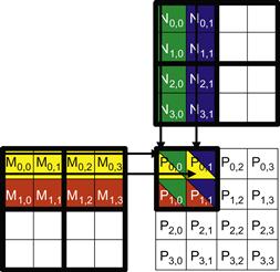
Figure 5.10 Tiling M and N matrices to utilize shared memory.
In Figure 5.10, we divide the M and N matrices into 2×2 tiles, as delineated by the thick lines. The dot product calculations performed by each thread are now divided into phases. In each phase, all threads in a block collaborate to load a tile of M elements and a tile of N elements into the shared memory. This is done by having every thread in a block to load one M element and one N element into the shared memory, as illustrated in Figure 5.11. Each row of Figure 5.11 shows the execution activities of a thread. Note that time progresses from left to right. We only need to show the activities of threads in block0,0; the other blocks all have the same behavior. The shared memory array for the M elements is called Mds. The shared memory array for the N elements is called Nds. At the beginning of phase 1, the four threads of block0,0 collaboratively load a tile of M elements into shared memory: thread0,0 loads M0,0 into Mds0,0, thread0,1 loads M0,1 into Mds0,1, thread1,0 loads M1,0 into Mds1,0, and thread1,1 loads M1,1 into Mds1,1. See the second column of Figure 5.11. A tile of N elements is also loaded in a similar manner, shown in the third column of Figure 5.11.
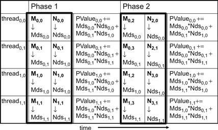
Figure 5.11 Execution phases of a tiled matrix multiplication.
After the two tiles of M and N elements are loaded into the shared memory, these values are used in the calculation of the dot product. Note that each value in the shared memory is used twice. For example, the M1,1 value, loaded by thread1,1 into Mds1,1, is used twice, once by thread0,1 and once by thread1,1. By loading each global memory value into shared memory so that it can be used multiple times, we reduce the number of accesses to the global memory. In this case, we reduce the number of accesses to the global memory by half. Readers should verify that the reduction is by a factor of N if the tiles are N×N elements.
Note that the calculation of each dot product in Figure 5.6 is now performed in two phases, shown as phase 1 and phase 2 in Figure 5.11. In each phase, products of two pairs of the input matrix elements are accumulated into the Pvalue variable. Note that Pvalue is an automatic variable so a private version is generated for each thread. We added subscripts just to clarify that these are different instances of the Pvalue variable created for each thread. The first phase calculation is shown in the fourth column of Figure 5.11; the second phase in the seventh column. In general, if an input matrix is of dimension N and the tile size is TILE_WIDTH, the dot product would be performed in N/TILE_WIDTH phases. The creation of these phases is key to the reduction of accesses to the global memory. With each phase focusing on a small subset of the input matrix values, the threads can collaboratively load the subset into the shared memory and use the values in the shared memory to satisfy their overlapping input needs in the phase.
Note also that Mds and Nds are reused to hold the input values. In each phase, the same Mds and Nds are used to hold the subset of M and N elements used in the phase. This allows a much smaller shared memory to serve most of the accesses to global memory. This is due to the fact that each phase focuses on a small subset of the input matrix elements. Such focused access behavior is called locality. When an algorithm exhibits locality, there is an opportunity to use small, high-speed memories to serve most of the accesses and remove these accesses from the global memory. Locality is as important for achieving high performance in multicore CPUs as in many-thread GPUs. We return to the concept of locality in Chapter 6.
We are now ready to present the tiled kernel function that uses shared memory to reduce the traffic to global memory. The kernel shown in Figure 5.12 implements the phases illustrated in Figure 5.11. In Figure 5.12, lines 1 and 2 declare Mds and Nds as shared memory variables. Recall that the scope of shared memory variables is a block. Thus, one pair of Mds and Nds will be created for each block and all threads of a block have access to the same Mds and Nds. This is important since all threads in a block must have access to the M and N values loaded into Mds and Nds by their peers so that they can use these values to satisfy their input needs.
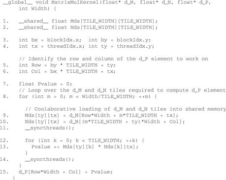
Figure 5.12 Tiled matrix multiplication kernel using shared memory.
#define TILE_WIDTH 16
Lines 3 and 4 save the threadIdx and blockIdx values into automatic variables and thus into registers for fast access. Recall that automatic scalar variables are placed into registers. Their scope is in each individual thread. That is, one private version of tx, ty, bx, and by is created by the runtime system for each thread. They will reside in registers that are accessible by one thread. They are initialized with the threadIdx and blockIdx values and used many times during the lifetime of the thread. Once the thread ends, the values of these variables also cease to exist.
Lines 5 and 6 determine the row index and column index of the d_P element that the thread is to produce. As shown in line 6, the horizontal (x) position, or the column index of the d_P element to be produced by a thread, can be calculated as bx∗TILE_WIDTH+tx. This is because each block covers TILE_WIDTH elements in the horizontal dimension. A thread in block bx would have bx blocks of threads, or (bx∗TILE_WIDTH) threads, before it; they cover bx∗TILE_WIDTH elements of d_P. Another tx thread within the same block would cover another tx element of d_P. Thus, the thread with bx and tx should be responsible for calculating the d_P element of which the xindex is bx∗TILE_WIDTH+tx. This horizontal index is saved in the variable Col (for column) for the thread and is also illustrated in Figure 5.13. For the example in Figure 5.10, the x index of the d_P element to be calculated by thread0,1 of block1,0 is 0×2+1=1. Similarly, the y index can be calculated as by∗TILE_WIDTH+ty. This vertical index is saved in the variable Row for the thread. Thus, as shown in Figure 5.10, each thread calculates the d_P element at the Col column and the Row row. Going back to the example in Figure 5.10, the y index of the d_P element to be calculated by thread1,0 of block0,1 is 1×2+0=2. Thus, the d_P element to be calculated by this thread is d_P2,1.
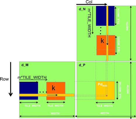
Figure 5.13 Calculation of the matrix indices in tiled multiplication.
Line 8 of Figure 5.12 marks the beginning of the loop that iterates through all the phases of calculating the final d_P element. Each iteration of the loop corresponds to one phase of the calculation shown in Figure 5.11. The m variable indicates the number of phases that have already been done for the dot product. Recall that each phase uses one tile of d_M and one tile of d_N elements. Therefore, at the beginning of each phase, m∗TILE_WIDTH pairs of d_M and d_N elements have been processed by previous phases.
In each phase, line 9 loads the appropriate d_M element into the shared memory. Since we already know the row of d_M and column of d_N to be processed by the thread, we will focus on the column index of d_M and row index of d_N. As shown in Figure 5.11, each block has TILE_WIDTH2 threads that will collaborate to load TILE_WIDTH2 d_M elements into the shared memory. Thus, all we need to do is to assign each thread to load one d_M element. This is conveniently done using the blockIdx and threadIdx. Note that the beginning column index of the section of d_M elements to be loaded is m∗TILE_WIDTH. Therefore, an easy approach is to have every thread load an element from at an offset tx that contains threadIdx.x value. This is precisely what we have in line 9, where each thread loads d_M[Row∗Width + m∗TILE_WIDTH + tx]. Since the value of Row is a linear function of ty, each of the TILE_WIDTH2 threads will load a unique d_M element into the shared memory. Together, these threads will load the dark square subset of d_M in Figure 5.13. Readers should use the small example in Figures 5.5 and 5.6 to verify that the address calculation works correctly.
The barrier __syncthreads() in line 11 ensures that all threads have finished loading the tiles of d_M and d_N into Mds and Nds before any of them can move forward. The loop in line 12 then performs one phase of the dot product based on these tile elements. The progression of the loop for thread(ty,tx) is shown in Figure 5.13, with the direction of d_M and d_N elements usage along the arrow marked with k, the loop variable in line 12. Note that these elements will be accessed from Mds and Nds, the shared memory arrays holding these d_M and d_N elements. The barrier __syncthreads() in line 14 ensures that all threads have finished using the d_M and d_N elements in the shared memory before any of them move on to the next iteration and load the elements in the next tiles. This way, none of the threads would load the elements too early and corrupt the input values for other threads.
After all sections of the dot product are complete, the execution exits the loop of line 8. All threads write to their d_P element using the Row and Col.
The benefit of the tiled algorithm is substantial. For matrix multiplication, the global memory accesses are reduced by a factor of TILE_WIDTH. If one uses 16×16 tiles, we can reduce the global memory accesses by a factor of 16. This increases the CGMA from 1 to 16. This improvement allows the memory bandwidth of a CUDA device to support a computation rate close to its peak performance. For example, this improvement allows a 150 GB/s global memory bandwidth to support (150/4)×16=600 GFLOPS!
5.5 Memory as a Limiting Factor to Parallelism
While CUDA registers and shared memory can be extremely effective in reducing the number of accesses to global memory, one must be careful not to exceed the capacity of these memories. These memories are forms of resources that are needed for thread execution. Each CUDA device offers a limited amount of resources, which limits the number threads that can simultaneously reside in the SM for a given application. In general, the more resources each thread requires, the fewer the number of threads can reside in each SM, and thus the fewer number of threads that can reside in the entire device.
Let’s use an example to illustrate the interaction between register usage of a kernel and the level of parallelism that a device can support. Assume that in a device D, each SM can accommodate up to 1,536 threads and has 16,384 registers. While 16,384 is a large number, it only allows each thread to use a very limited number of registers considering the number of threads that can reside in each SM. To support 1,536 threads, each thread can use only 16,384÷1,536=10 registers. If each thread uses 11 registers, the number of threads able to be executed concurrently in each SM will be reduced. Such reduction is done at the block granularity. For example, if each block contains 512 threads, the reduction of threads will be done by reducing 512 threads at a time. Thus, the next lower number of threads from 1,536 would be 512, a one-third reduction of threads that can simultaneously reside in each SM. This can greatly reduce the number of warps available for scheduling, thus reducing the processor’s ability to find useful work in the presence of long-latency operations.
Note that the number of registers available to each SM varies from device to device. An application can dynamically determine the number of registers available in each SM of the device used and choose a version of the kernel that uses the number of registers appropriate for the device. This can be done by calling the cudaGetDeviceProperties() function, the use of which was discussed in Section 4.6. Assume that variable &dev_prop is passed to the function for the device property, and the field dev_prop.regsPerBlock gives the number of registers available in each SM. For device D, the returned value for this field should be 16,384. The application can then divide this number by the target number of threads to reside in each SM to determine the number of registers that can be used in the kernel.
Shared memory usage can also limit the number of threads assigned to each SM. Assume device D has 16,384 (16 K) bytes of shared memory in each SM. Keep in mind that shared memory is used by blocks. Assume that each SM can accommodate up to eight blocks. To reach this maximum, each block must not use more than 2 K bytes of shared memory. If each block uses more than 2 K bytes of memory, the number of blocks that can reside in each SM is such that the total amount of shared memory used by these blocks does not exceed 16 K bytes. For example, if each block uses 5 K bytes of shared memory, no more than three blocks can be assigned to each SM.
For the matrix multiplication example, shared memory can become a limiting factor. For a tile size of 16×16, each block needs a 16×16×4=1 K bytes of storage for Mds. Another 1 KB is needed for Nds. Thus, each block uses 2 K bytes of shared memory. The 16 K–byte shared memory allows eight blocks to simultaneous reside in an SM. Since this is the same as the maximum allowed by the threading hardware, shared memory is not a limiting factor for this tile size. In this case, the real limitation is the threading hardware limitation that only 768 threads are allowed in each SM. This limits the number of blocks in each SM to three. As a result, only 3×2 KB=6 KB of the shared memory will be used. These limits do change from device generation to the next but are properties that can be determined at runtime, for example, the GT200 series of processors can support up to 1,024 threads in each SM.
Note that the size of shared memory in each SM can also vary from device to device. Each generation or model of device can have a different amount of shared memory in each SM. It is often desirable for a kernel to be able to use a different amount of shared memory according to the amount available in the hardware. That is, we may want to have a kernel to dynamically determine the size of the shared memory and adjust the amount of shared memory used. This can be done by calling the cudaGetDeviceProperties() function, the general use of which was discussed in Section 4.6. Assume that variable &dev_prop is passed to the function, the field dev_prop.sharedMemPerBlock gives the number of registers available in each SM. The programmer can then determine the number of amount of shared memory that should be used by each block.
Unfortunately, the kernel in Figure 5.12 does not support this. The declarations used in Figure 5.12 hardwire the size of its shared memory usage to a compile-time constant:
__shared__ float Mds[TILE_WIDTH][TILE_WIDTH];
__shared__ float Nds[TILE_WIDTH][TILE_WIDTH];
That is, the size of Mds and Nds is set to be TILE_WIDTH2 elements, whatever the value of TILE_WIDTH is set to be at compile time. For example, assume that the file contains
#define TILE_WIDTH 16
Both Mds and Nds will have 256 elements. If we want to change the size of Mds and Nds, we need to change the value of TILE_WIDTH and recompile. The kernel cannot easily adjust its shared memory usage at runtime without recompilation. We can enable such adjustment with a different style of declaration in CUDA. We can add a C extern keyword in front of the shared memory declaration and omit the size of the array in the declaration. Based on this style, the declaration for Mds and Nds become:
extern __shared__ Mds[];
extern __shared__ Nds[];
Note that the arrays are now one dimensional. We will need to use a linearized index based on the vertical and horizontal indices.
At runtime, when we launch the kernel, we can dynamically determine the amount of shared memory to be used according to the device query result and supply that as a third configuration parameter to the kernel launch. For example, the kernel launch statement in Figure 4.18 could be replaced with the following statements:
size_t size =
calculate_appropriate_SM_usage(dev_prop.sharedMemPerBlock,…);
matrixMulKernel<<<dimGrid, dimBlock, size>>>(Md, Nd, Pd, Width);
where size_t is a built-in type for declaring a variable to hold the size information for dynamically allocated data structures. We have omitted the details of the calculation for setting the value of size at runtime.
5.6 Summary
In summary, CUDA defines registers, shared memory, and constant memory that can be accessed at a higher speed and in a more parallel manner than the global memory. Using these memories effectively will likely require redesign of the algorithm. We use matrix multiplication as an example to illustrate tiled algorithms, a popular strategy to enhance locality of data access and enable effective use of shared memory. We demonstrate that with 16×16 tiling, global memory accesses are no longer the major limiting factor for matrix multiplication performance.
It is, however, important for CUDA programmers to be aware of the limited sizes of these types of memory. Their capacities are implementation dependent. Once their capacities are exceeded, they become limiting factors for the number of threads that can be simultaneously executing in each SM. The ability to reason about hardware limitations when developing an application is a key aspect of computational thinking. Readers are also referred to Appendix B for a summary of resource limitations of several different devices.
Although we introduced tiled algorithms in the context of CUDA programming, it is an effective strategy for achieving high performance in virtually all types of parallel computing systems. The reason is that an application must exhibit locality in data access to make effective use of high-speed memories in these systems. For example, in a multicore CPU system, data locality allows an application to effectively use on-chip data caches to reduce memory access latency and achieve high performance. Therefore, readers will find the tiled algorithm useful when they develop a parallel application for other types of parallel computing systems using other programming models.
Our goal for this chapter is to introduce the different types of CUDA memory. We introduced tiled algorithm as an effective strategy for using shared memory. We have not discussed the use of constant memory, which will be explained in Chapter 8.
5.7 Exercises
5.1. Consider the matrix addition in Exercise 3.1. Can one use shared memory to reduce the global memory bandwidth consumption? Hint: analyze the elements accessed by each thread and see if there is any commonality between threads.
5.2. Draw the equivalent of Figure 5.6 for a 8×8 matrix multiplication with 2×2 tiling and 4×4 tiling. Verify that the reduction in global memory bandwidth is indeed proportional to the dimension size of the tiles.
5.3. What type of incorrect execution behavior can happen if one forgots to use syncthreads() in the kernel of Figure 5.12?
5.4. Assuming capacity was not an issue for registers or shared memory, give one case that it would be valuable to use shared memory instead of registers to hold values fetched from global memory? Explain your answer.
5.5. For our tiled matrix–matrix multiplication kernel, if we use a 32×32 tile, what is the reduction of memory bandwidth usage for input matrices M and N?
5.6. Assume that a kernel is launched with 1,000 thread blocks each of which has 512 threads. If a variable is declared as a local variable in the kernel, how many versions of the variable will be created through the lifetime of the execution of the kernel?
5.7. In the previous question, if a variable is declared as a shared memory variable, how many versions of the variable will be created through the lifetime of the execution of the kernel?
5.8. Explain the difference between shared memory and L1 cache.
5.9. Consider performing a matrix multiplication of two input matrices with dimensions N×N. How many times is each element in the input matrices requested from global memory when:
b. Tiles of size T×T are used?
5.10. A kernel performs 36 floating-point operations and 7 32-bit word global memory accesses per thread. For each of the following device properties, indicate whether this kernel is compute- or memory-bound.
a. Peak FLOPS=200 GFLOPS, peak memory bandwidth=100 GB/s.
b. Peak FLOPS=300 GFLOPS, peak memory bandwidth=250 GB/s.
5.11. Indicate which of the following assignments per streaming multiprocessor is possible. In the case where it is not possible, indicate the limiting factor(s).
a. 4 blocks with 128 threads each and 32 B shared memory per thread on a device with compute capability 1.0.
b. 8 blocks with 128 threads each and 16 B shared memory per thread on a device with compute capability 1.0.
c. 16 blocks with 32 threads each and 64 B shared memory per thread on a device with compute capability 1.0.
d. 2 blocks with 512 threads each and 32 B shared memory per thread on a device with compute capability 1.2.
e. 4 blocks with 256 threads each and 16 B shared memory per thread on a device with compute capability 1.2.
f. 8 blocks with 256 threads each and 8 B shared memory per thread on a device with compute capability 1.2.
1See the CUDA Programming Guide for zero-copy access to the global memory.
2There are some exceptions to this rule. The compiler may decide to store an automatic array into registers if all accesses are done with constant index values.
3Note that one can use CUDA memory fencing to ensure data coherence between thread blocks if the number of thread blocks is smaller than the number of SMs in the CUDA device. See the CUDA Programming Guide for more details.