
Chapter 7
Countermeasures against Side-Channel Analysis and Fault Analysis
In order to overcome the side-channel attacks and the fault attacks introduced in Chapters 5 and 6, this chapter explains several countermeasures. There exist many possible countermeasures depending on the abstraction level in cryptosystems. Figure 7.1 describes the hierarchy of the cryptosystem, and the position of logic-level countermeasures for hardware implementations.

Figure 7.1 Countermeasures for side-channel analysis and fault analysis
The hardware device can counteract the side-channel attack if the countermeasure is appropriately implemented in the lowest abstraction level, that is, in the logic level. Such a logic-level countermeasure not only protects the logical gates but also helps to enhance the security of cryptographic algorithm and protocol against side-channel attacks, which is one of the most advantageous points of applying the countermeasure to the logic level. In general, the side-channel countermeasure tends to be more ineffective if implementing it in a higher level because higher level countermeasures cannot take care of all leakage sources that exist all over the circuits consisting of logical gates. Therefore, this chapter mainly explains the logic-level countermeasure using hiding logics and masking logics. The concept of higher level countermeasures is also explained especially focusing on the fault attack countermeasures since faults can be detected at each abstraction level, several countermeasures for the fault detection can be implemented.
7.1 Logic-Level Hiding Countermeasures
There are two major techniques to implement a logic-level countermeasure; hiding logics and masking logics. Here, several representative countermeasures are introduced as a case study in order to understand their resistance against the side-channel attacks.
7.1.1 Overview of Hiding Countermeasure with WDDL Technique
A countermeasure using the hiding logics aims to make the side-channel information uniform. More specifically, in the case that the power consumption is used as side-channel information, the hiding logics are expected to consume constant power for any input values. This makes the attacker difficult to derive the sensitive information, for example, intermediate values during the cryptographic operations via side-channel analysis.
One possible solution to realize such hiding logics is to implement logical gates that consume constant power regardless of the inputs. By doing so, any combinatorial logics, which use those constant-power gates as building blocks, will consume constant power. Wave dynamic differential logic (WDDL) is a representative technique that follows the above concept, which was proposed by Tiri and Verbauwhede (2004).

Figure 7.2 Example circuit with WDDL technique (state 0, precharge phase)
Figure 7.2 illustrates an example circuit with the WDDL technique that is one of the dual-rail logics. The signals propagating on the bold line deal with values operated with positive logic, and the signals on the normal line transfers values performed with negative logic. One-bit signal, a, is represented with two one-bit signals as ![]() for the input and output of the WDDL gates. Since the Hamming weight of the pair,
for the input and output of the WDDL gates. Since the Hamming weight of the pair, ![]() , is always 1, all the WDDL gates are balanced in terms of the number of ones and zeros in the signals. Moreover, the number of input and output signals for the WDDL gate is twice as many as the normal (single-rail) gate. As can be seen from Figure 7.2, the WDDL-NAND and WDDL-NOR gates have four inputs and two outputs, whereas the WDDL-INV gate has two inputs and two outputs. The sequential logic in the circuit named DFFP is a DFF with precharge logics. The details of DFFP are explained later in this chapter. For the purpose of initializing the circuit with the WDDL technique, DFFP outputs a special paired value,
, is always 1, all the WDDL gates are balanced in terms of the number of ones and zeros in the signals. Moreover, the number of input and output signals for the WDDL gate is twice as many as the normal (single-rail) gate. As can be seen from Figure 7.2, the WDDL-NAND and WDDL-NOR gates have four inputs and two outputs, whereas the WDDL-INV gate has two inputs and two outputs. The sequential logic in the circuit named DFFP is a DFF with precharge logics. The details of DFFP are explained later in this chapter. For the purpose of initializing the circuit with the WDDL technique, DFFP outputs a special paired value, ![]() , called precharge value. The precharge value of
, called precharge value. The precharge value of ![]() propagates through the combinatorial logics since any WDDL gates output
propagates through the combinatorial logics since any WDDL gates output ![]() when the precharge values are provided as its inputs. As a result, all the signals in the combinatorial circuit are initialized to zeros. Such a circuit state is denoted by state 0 here. The state 0 will be kept during the time period called precharge phase. Figure 7.2 shows the signal values in the combinatorial logics in the precharge phase.
when the precharge values are provided as its inputs. As a result, all the signals in the combinatorial circuit are initialized to zeros. Such a circuit state is denoted by state 0 here. The state 0 will be kept during the time period called precharge phase. Figure 7.2 shows the signal values in the combinatorial logics in the precharge phase.
After the precharge phase, evaluation phase starts. In the evaluation phase, DFFP provides the pair of ![]() that is either
that is either ![]() or
or ![]() . For instance, three left-side DFFPs provide
. For instance, three left-side DFFPs provide ![]() ,
, ![]() , and
, and ![]() beginning at the top as shown in Figure 7.3. In this case, the WDDL-NAND operation in the center of the figure outputs
beginning at the top as shown in Figure 7.3. In this case, the WDDL-NAND operation in the center of the figure outputs ![]() based on the NAND operation on two inputs
based on the NAND operation on two inputs ![]() and
and ![]() . In this way, all the signals are determined in the combinatorial logics. Let us call this state as state A. Figure 7.4 shows another result of the evaluation phase. Based on the evaluation for
. In this way, all the signals are determined in the combinatorial logics. Let us call this state as state A. Figure 7.4 shows another result of the evaluation phase. Based on the evaluation for ![]() ,
, ![]() , and
, and ![]() for the left-side DFFPs, the example circuit goes to state B by a state transition. Note that the number of possible states is eight in total since the left-side DFFPs can provide eight different paired values.
for the left-side DFFPs, the example circuit goes to state B by a state transition. Note that the number of possible states is eight in total since the left-side DFFPs can provide eight different paired values.

Figure 7.4 Example circuit with WDDL technique (state B, evaluation phase)
In order to see the role of the precharge phase, let us simulate the power consumption consumed by the state transition. In the case that the state transition from state A to state B occurs in a consecutive clock cycle, the amount of signal toggles from 0 to 1 and from 1 to 0 both become six. Therefore, we would observe the power consumption corresponding to the number of signal toggles. On the other hand, when the state transition from state A to state A happen to occur in consecutive clock cycles, the values are not changed at all in the combinatorial logics, which leads to no power consumption. This observation infers that the power consumption is dependent on the state transitions. Therefore, this could be the vulnerability against the side-channel attacks. Suppose that state 0 in the precharge phase is processed between states A and B, that is, transitions of states A, 0, and B in sequence. From state A to state 0, the amount of signal toggles from 1 to 0 is six, and 0-to-1 signal toggles never happen. From state 0 to state B, the amount of signal toggles from 0 to 1 is six, and 1-to-0 signal toggles never happen. The same results will be obtained even for the case of the transitions of states A, 0, and A. Furthermore, this result holds even if different values are provided from the DFFPs. That is to say, state 0 in the precharge phase plays an important role to make power consumption constant.

Figure 7.3 Example circuit with WDDL technique (state A, evaluation phase)
7.1.2 WDDL-NAND Gate
Based on the explanations of the circuit with the WDDL technique, the details of the WDDL gates are explained here. It is found that there exist several constraints for the WDDL gates to guarantee the constant power consumption. The WDDL-NAND gate illustrated in Figure 7.5 satisfies all the constraints mentioned in the previous section. The positive-logic operation is performed with the AND gate and the negative-logic operation is done with the OR gate in this case. Then, the output wires of the AND and OR gates are crossed so that the positiveand negative values are switched. The operation of the WDDL-NAND gate during the evaluation phase is defined as

The straightforward implementation for the WDDL-NAND would be to use the NAND gate. Nevertheless, the reason why the AND gate is used instead of the NAND gate in implementing the WDDL-NAND gate shown in Figure 7.5 is to make all the signals as zeros in the precharge phase.

Figure 7.5 The WDDL-NAND gate for zero-precharge case
As shown in Figure 7.5, signals behave specially in the precharge phase. Therefore, Equation (7.1) holds only in the evaluation phase. In the precharge phase, all inputs for the WDDL-NAND are zeros, and hence the outputs also become zero. Alternation of the precharge and evaluation phases is the key to the solution for constant power consumption.
7.1.3 WDDL-NOR and WDDL-INV Gates
In a similar manner, the operation of the WDDL-NOR gate in the evaluation phase is defined as

Note that the WDDL-INV gate does not require any operational logic gate. It is realized with the crossed wiring as shown in Figure 7.6. Figure 7.7 shows the pseudo-Verilog code for WDDL-NAND, WDDL-NOR, and WDDL-INV gates.

Figure 7.6 The WDDL-AND, WDDL-NOR, and WDDL-INV gates
// Data signals are represented with two bits as
// signal = {positive bit, negative bit}
module wddl_nand (a, b, c);
   input [1:0] a, b;
   output [1:0] c;
   assign c[0] = a[1] & b[1];
   assign c[1] = a[0] | b[0];
 endmodule
 module wddl_nor (a, b, c);
   input [1:0] a, b;
   output [1:0] c;
   assign c[0] = a[1] | b[1];
   assign c[1] = a[0] & b[0];
 endmodule
 module wddl_inv (a, c);
   input [1:0] a;
   output [1:0] c;
   assign c[0] = a[1];
   assign c[1] = a[0];
 endmodule
Figure 7.7 Pseudo-Verilog code for WDDL NAND, NOR, and INV gates
7.1.4 Precharge Logic for WDDL Technique
Precharge is essential for circuits with the WDDL technique in order to guarantee the constant Hamming weight of the signals. Figure 7.8 shows a precharge logic that outputs zeros when a precharge signal, ![]() , is high. When
, is high. When ![]() is low, it provides the values of DFFPs. Figure 7.9 shows a pseudo-Verilog code for DFFP.
is low, it provides the values of DFFPs. Figure 7.9 shows a pseudo-Verilog code for DFFP.

Figure 7.8 Precharge logics for circuits with WDDL gates
module wddl_precharge (clk, rst_n, pre, d_in, d_pre);
   input pre; // Precharge signal
   input [1:0] d_in; // Input data for DFF
   output [1:0] d_pre; // Output data with precharge
   reg [1:0] d_out; // Output data of DFF
   always @(posedge clk or negedge rst_n) begin
     if (rst_n == 0)
       d_out <= 0;
     else
       d_out <= d_in;
   end
   assign d_pre[0] = (d_out[1] | pre);
   assign d_pre[1] = (d_out[0] | pre);
 endmodule
Figure 7.9 Pseudo-Verilog code for DFF with precharge logics (DFFP)
The precharge effects spread to the entire combinatorial logics consisting of the WDDL gates, so that all of the input and output signals of the WDDL gates become zeros. From the electrical point of view, this physical action corresponds to discharge. After precharging, ![]() becomes low and the combinatorial circuits start being evaluated based on the values provided from DFFs. In this phase, exactly a half of the signals become ones, whereas the rest of the signals stay zeros, which contributes to constant power consumption. Figure 7.10 explains the details.
becomes low and the combinatorial circuits start being evaluated based on the values provided from DFFs. In this phase, exactly a half of the signals become ones, whereas the rest of the signals stay zeros, which contributes to constant power consumption. Figure 7.10 explains the details.
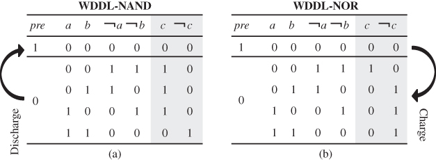
Figure 7.10 Signal toggles for (a) charge and (b) discharge of WDDL gates
When ![]() is low, Hamming weight of signals for the WDDL-NAND and WDDL-NOR gates is both 3, and when
is low, Hamming weight of signals for the WDDL-NAND and WDDL-NOR gates is both 3, and when ![]() is high, that is, Hamming weight is 0 as all the signals become zeros. Therefore, regardless of the input values, we know that the WDDL gate consumes constant power corresponding to Hamming weight of 3. Furthermore, constant current is expected to flow to the ground when discharging.
is high, that is, Hamming weight is 0 as all the signals become zeros. Therefore, regardless of the input values, we know that the WDDL gate consumes constant power corresponding to Hamming weight of 3. Furthermore, constant current is expected to flow to the ground when discharging.
However, in the real world, constant power is realized with an equivalent power consumption of the signal wires in the WDDL circuits. The significant challenge in the wire routing is to equalize the wire load capacitance of wires for c and ![]() , that is,
, that is, ![]() , as illustrated in Figure 7.11. Therefore, the WDDL circuit layout should be carefully taken care.
, as illustrated in Figure 7.11. Therefore, the WDDL circuit layout should be carefully taken care.

Figure 7.11 Wire load capacitance in WDDL gate
7.1.5 Intrinsic Fault Detection Mechanism of WDDL
The WDDL gates can easily detect a fault due to the nature of dual-rail logic. The WDDL gate operates one bit-wise operation twice in the positive and negative values at the same time. If one of the positive and negative logics has error, the output, ![]() becomes
becomes ![]() or
or ![]() that never happens in a proper computation.1 For instance, by checking the XOR of c and
that never happens in a proper computation.1 For instance, by checking the XOR of c and ![]() , one can provide information whether or not an error occurs. Upon the detection of the error, a cryptographic hardware can be stopped so that any useful information to the attacker does not leak. By doing so, differential fault analysis cannot work since it requires a ciphertext generated in the erroneous computation.
, one can provide information whether or not an error occurs. Upon the detection of the error, a cryptographic hardware can be stopped so that any useful information to the attacker does not leak. By doing so, differential fault analysis cannot work since it requires a ciphertext generated in the erroneous computation.
7.2 Logic-Level Masking Countermeasures
7.2.1 Overview of Masking Countermeasure
Masking countermeasures mask an intermediate variable, a, with a random number, r, which is called mask. The main purpose of the masking countermeasure is to make the intermediate values uncorrelated with side-channel information. That is, as far as using a fresh random number, the masked intermediate value is represented differently, which makes the side-channel attack difficult. In general, the freshness of the random number in the masking countermeasure has a significant impact on side-channel resistance. Therefore, reuse of random numbers should be avoided, and change of the random number should be performed frequentlyenough.

Figure 7.12 Boolean masking of n-bit signal
There are several kinds of masking operations such as Boolean masking and arithmetic masking. Boolean masking uses bitwise XOR operation, that is, addition over ![]() as
as
where ![]() is a masked value of a and r is a random number (mask).
is a masked value of a and r is a random number (mask).
On the contrary, arithmetic masking for a value, a is obtained with
where n is the bit length of a and r. This type of masking can be used for block ciphers that employ modular additions in the algorithm.
Both types of masking scheme can decrease the correlation between the side-channel information from a device and intermediate values on wires in a hardware implementation. This makes the side-channel attack difficult. Hereafter, we focus on Boolean masking since it is a fundamental technique for many block ciphers including AES.
7.2.2 Operations on Values with Boolean Masking
Operations on values with Boolean masking are explained here. Suppose that a masked value, ![]() , is operated with a Boolean function, f. That is,
, is operated with a Boolean function, f. That is,
This equation indicates that the mask, r, cannot be easily removed or changed after operating the function, f, since r cannot be got rid of from ![]() with a simple operation.
with a simple operation.
If f is a linear function, the Equation (7.5) becomes as
It can be seen that operations on masked values using linear functions can be implemented with performing f twice. Accordingly, the mask can be easily removed or changed simply with the XOR operation. Therefore, another random bit ![]() can be replaced with r easily since
can be replaced with r easily since
In this form, further operations can be continued on the masked values.
From the observation, we know that the challenge in the masking countermeasures is to implement nonlinear functions efficiently.
7.2.3 Re-masking and Unmasking
The necessity of changing the mask and removing the mask is explained by using the example case of the ![]() transformation of AES-128. More specifically, we consider the case when f is the addition in
transformation of AES-128. More specifically, we consider the case when f is the addition in ![]() , that is, 128-bit XOR operation.
, that is, 128-bit XOR operation.
Suppose that the ![]() transformation takes masked values,
transformation takes masked values, ![]() , and a subkey,
, and a subkey, ![]() , as its input data, and perform the XOR operation, that is,
, as its input data, and perform the XOR operation, that is, ![]() .
.
The output value of ![]() transformation is also masked with the same random bits as used for the input value because
transformation is also masked with the same random bits as used for the input value because
where ![]() is the result of the
is the result of the ![]() transformation. Therefore, neither hardware overhead nor additional computation is required.
transformation. Therefore, neither hardware overhead nor additional computation is required.
However, from the view point of side-channel leakage, the random bits should be refreshed frequently in order to reduce the risk of leaking the information of the random bits. Refreshing the mask is easily realized with XOR operation as illustrated in Figure 7.13 that shows an example for the re-masking. The masked value, ![]() , is re-masked with a fresh random bit,
, is re-masked with a fresh random bit, ![]() , and
, and ![]() is output.
is output.
The operation order must be taken care so that the unmasked value, a, never appears on any operations.2 In other words, all of the operations have to use the masked values.

Figure 7.13 Re-masking of n-bit signal
The masked values are also easily unmasked simply with XOR operations as shown in Figure 7.14. Note that unmasking should appear only in the last stage of a cipher operation such as after the ![]() transformation of the last round of AES. Again, if unmasked value appears on a wire and if it contains sensitive information, the attacker can recover the sensitive information via side-channel analysis.
transformation of the last round of AES. Again, if unmasked value appears on a wire and if it contains sensitive information, the attacker can recover the sensitive information via side-channel analysis.

Figure 7.14 Unmasking of n-bit signal
7.2.4 Masked AND Gate
One possible implementation for the AND operations on values with Boolean masking is called Masked AND operation, which was proposed by Trichina et al. (2005). This gate-level masking can facilitate the difficulty in building up nonlinear functions that deals with Boolean masking values. Figure 7.15 illustrates the masked AND gates. The masked AND performs the AND operation on masked inputs, ![]() and
and ![]() , with refreshing the mask using
, with refreshing the mask using ![]() as
as

Figure 7.15 Masked AND gate
There are five inputs, ![]() ,
, ![]() ,
, ![]() ,
, ![]() , and
, and ![]() , that are operated to generate outputs,
, that are operated to generate outputs, ![]() and
and ![]() . The order of the XOR operations has special importance for reducing the threat against the side-channel attacks. More specifically, one has to be careful in choosing the order of operations so that unmasked values are not observed on any wire between gates. Figure 7.16 describes the pseudo-Verilog code for the masked AND operation.
. The order of the XOR operations has special importance for reducing the threat against the side-channel attacks. More specifically, one has to be careful in choosing the order of operations so that unmasked values are not observed on any wire between gates. Figure 7.16 describes the pseudo-Verilog code for the masked AND operation.
module Masked_AND (a_r1, b_r2, r1, r2, r3, c_r3);
   input a_r1, b_r2; // Masked inputs
   input r1, r2, r3; // Random bits for mask
   output r3, c_r3; // Masked output with fresh mask
   wire w1, w2, …, w7;
   assign w1 = r1 & r2;
   assign w2 = r1 & b_r2;
   assign w3 = a_r1 & r2;
   assign w4 = a_r1 & b_r2;
   assign w5 = r3 ^ w1;
   assign w6 = w5 ^ w2;
   assign w7 = w6 ^ w3;
   assign c_r3 = w7 ^ w4;
 endmodule
Figure 7.16 Pseudo-Verilog code for masked AND gate
7.2.5 Random Switching Logic
The random switching logic (RSL) technique is another famous masking countermeasure, which was proposed by Suzuki et al. (2004) and Saeki et al. (2009). RSL can be implemented with a standard-cell-based library. Figure 7.17 illustrates a NAND gate realized with the standard-cell-based RSL technique.

Figure 7.17 Standard-cell-based RSL-NAND
The RSL-NAND gate has six inputs and two outputs. The inputs, ![]() and
and ![]() , are data signals for a and b that are masked with
, are data signals for a and b that are masked with ![]() and
and ![]() , respectively. The masked signals are re-masked with a fresh random bit,
, respectively. The masked signals are re-masked with a fresh random bit, ![]() , and the result of the NAND operation for a and b are performed. Another input signal,
, and the result of the NAND operation for a and b are performed. Another input signal, ![]() , is used for suppressing the propagation of the glitch signals generated in the RSL-NAND gate. In other words,
, is used for suppressing the propagation of the glitch signals generated in the RSL-NAND gate. In other words, ![]() should be low until all the evaluation of the signals in the RSL-NAND operations completes. The pseudo-Verilog code for the RSL-NAND gate is described in Figure 7.18.
should be low until all the evaluation of the signals in the RSL-NAND operations completes. The pseudo-Verilog code for the RSL-NAND gate is described in Figure 7.18.
module RSL_NAND (a_r1, b_r2, r1, r2, r3, c_r3);
   input a_r1, b_r2; // Masked inputs
   input r1, r2, r3; // Random bits for mask
   input en; // For gating the output
   output r3, c_r3; // Masked output with fresh masking
   wire w1, w2, …, w6;
   wire a_r3, b_r3;
   assign w1 = r1 ^ r3; // Re-masking
   assign a_r3 = w1 ^ a_r1;
   assign w2 = r2 ^ r3;
   assign b_r3 = w2 ^ b_r2;
   assign w3 = a_r3 | b_r3;
   assign w4 = b_r3 | r3;
   assign w5 = r3 | a_r3;
   assign w6 = (w3 ^ w4 ^ w5); // Minority logic
   assign c_r3 = en ^ w6; // Output gating
 endmodule
Figure 7.18 Pseudo-Verilog code for RSL-NAND gate
7.2.6 Threshold Implementation
Threshold implementation or TI is a masking method based on secret sharing, which is proven to be resistant against the first-order side-channel attacks even in the presence of signal glitches. TI was proposed by Nikova et al. (2006). Notice that TI is one of the first countermeasures that overcome the vulnerability caused by the glitch signals fundamentally. TI has a characteristic that the intermediate value can be masked not only by one random value but by two or more of them, depending on the number of shares.
For the same reason as other masking schemes, TI can be easily applied to the linear transformation. Therefore, the focus of TI is on how to mask the nonlinear transformation. The basic principle of TI can be summarized as follows. Each input variable of a nonlinear transformation is separated into several shares such that the addition over ![]() of the shares equals to the input data. That is, the nonlinear transformation is separated into several functions.3 Each function uses the shares of input to perform the calculation, and the addition over
of the shares equals to the input data. That is, the nonlinear transformation is separated into several functions.3 Each function uses the shares of input to perform the calculation, and the addition over ![]() for the outputs of all functions is the expected output. In order to make TI resistant against the first-order side-channel attacks, one has to assure that for every input variable of each function, all of the shares are not used. By doing so, one can ensure that the calculation of each function is independent from the original input variables, and hence the first-order side-channel resistance is achieved.
for the outputs of all functions is the expected output. In order to make TI resistant against the first-order side-channel attacks, one has to assure that for every input variable of each function, all of the shares are not used. By doing so, one can ensure that the calculation of each function is independent from the original input variables, and hence the first-order side-channel resistance is achieved.
Let us take the AND gate, ![]() , as an example. One can separate each input variable into three shares, that is,
, as an example. One can separate each input variable into three shares, that is, ![]() and
and ![]() . The calculation of the TI-AND gate can be realized with three functions as
. The calculation of the TI-AND gate can be realized with three functions as
One can see that ![]() does not use shares,
does not use shares, ![]() and
and ![]() , so
, so ![]() is independent from x and y. Similarly, it can be found that
is independent from x and y. Similarly, it can be found that ![]() and
and ![]() are also independent from x and y. The addition of shares over
are also independent from x and y. The addition of shares over ![]() ,
, ![]() ,
, ![]() and
and ![]() , is
, is
Therefore, operations corresponding to Equations (7.17)–(7.19) can be regarded as a split computation of the AND operation based on the secret sharing scheme with three shares. Figure 7.20 shows the block diagram for the TI-AND gate, and Figure 7.21 describes the corresponding pseudo-Verilog code.

Figure 7.20 Shared AND gate with TI technique
module Shared_AND (x_1, x_2, x_3, y_1, y_2, y_3, s_1, s_2, s_3);
// x and y are split into three shares as
// x = x_3, x_2, x_1 and y = y_3, y_2, y_1
   input [3:1] x, y;
   output [3:1] s;
   wire w1, w2, …, w9;
   assign w1 = x[2] & y[2];
   assign w2 = x[2] & y[3];
   assign w3 = x[3] & y[2];
   assign s[1] = w1 ^ w2 ^ w3;
   assign w4 = x[3] & y[3];
   assign w5 = x[1] & y[3];
   assign w6 = x[3] & y[1];
   assign s[2] = w4 ^ w5 ^ w6;
   assign w7 = x[1] & y[1];
   assign w8 = x[1] & y[2];
   assign w9 = x[2] & y[1];
   assign s[3] = w7 ^ w8 ^ w9;
 endmodule
Figure 7.21 Pseudo-Verilog code for shared AND gate with TI technique
7.3 Higher Level Countermeasures
The gate-level countermeasures require a significant degradation of the speed performance and hardware cost. This motivates us to consider algorithm-level countermeasures that are normally cost-effective compared to the gate-level countermeasures. In the algorithm-level countermeasures, a range of protection is in units of a composite operation that consists of multiple logical gates in hardware. An algorithm-oriented optimization is often possible, and a better trade-off between performance and cost is likely to be improved compared to the gate-level countermeasures.
Differences between architecture- and algorithm-level countermeasures are not so clear since they are tightly related to the type of computation and its grain size. However, in one perspective, the architecture-level countermeasure can be regarded as a hardware architecture that offers the resistance against the side-channel and/or fault attacks regardless of the performed algorithm. For instance, a general-purpose CPU implemented with the logic-level countermeasure such as the WDDL technique could offer the architecture-level countermeasure to any software implementation. For another example, a current equalizer circuit to isolate the critical encryption/decryption activity can be considered one of the architecture-level countermeasures in terms of preventing the power analysis attacks.4 One example was shown by Tokunaga and Blaauw (2009).
In this section, countermeasure at each abstraction level is explained together with several examples. Especially, countermeasures for the fault attacks are focused on since the fault can be detected at any abstraction level. On the other hand, higher the abstraction level becomes, more difficult the side-channel countermeasure tendsto be. This is because the side-channel attack exploits the gate-level information leakage, and hence a countermeasure is necessary in the lowest abstraction level.
7.1 Algorithm-Level Countermeasures
The masking countermeasures such as the masked AND and TI are not necessary to be implemented in the gate level. For instance, as for the masked AND technique, Equation (7.10) holds even if the bitwise AND and XOR operations are replaced with n-bit multiplication and addition in ![]() , respectively as
, respectively as
where the operators, “![]() ” and “
” and “![]() ” respectively are multiplication and addition in
” respectively are multiplication and addition in ![]() with an irreducible polynomial,
with an irreducible polynomial, ![]() , whose degree is n.
, whose degree is n. ![]() ,
, ![]() , and
, and ![]() are n-bit random numbers used for masking n-bit multiplication in
are n-bit random numbers used for masking n-bit multiplication in ![]() of
of ![]() .
.
Figure 7.22 illustrates the block diagram for masked multiplication in ![]() . Notice that it consists of four normal multiplication modules and four normal additions that are simply realized with XOR gates. That is, there is some flexibility in choosing a multiplication module. Figure 7.23 describes a pseudo-Verilog code for masked multiplier in
. Notice that it consists of four normal multiplication modules and four normal additions that are simply realized with XOR gates. That is, there is some flexibility in choosing a multiplication module. Figure 7.23 describes a pseudo-Verilog code for masked multiplier in ![]() .
.

Figure 7.22 Masked modular multiplication in 
module MM (A, B, C);
   input [n-1:0] A, B;
   output [n-1:0] C;
   //Description for multiplication in
   //Irreducible polynomial, for example,
 endmodule
 module Masked_MM (A_R1, B_R2, R1, R2, R3, C_R3);
   input [n-1:0] A_R1, B_R2; // Masked inputs
   input [n-1:0] R1, R2, R3; // Random bits for mask
   output [n-1:0] C_R3; // Masked output with fresh masking
   wire [n-1:0] W1, W2, …, W7;
   MM MM1 (R1, R2, W1);
   MM MM2 (R1, B_R2, W2);
   MM MM3 (A_R1, R2, W3);
   MM MM4 (A_R1, B_R2, W4);
   assign W5 = R3 ^ W1;
   assign W6 = W5 ^ W2;
   assign W7 = W6 ^ W3;
   assign C_R3 = W7 ^ W4;
 endmodule
endmodule
module Masked_MM (A_R1, B_R2, R1, R2, R3, C_R3);
input [n-1:0] A_R1, B_R2; // Masked inputs
input [n-1:0] R1, R2, R3; // Random bits for mask
output [n-1:0] C_R3; // Masked output with fresh masking
wire [n-1:0] W1, W2, …, W7;
MM MM1 (R1, R2, W1);
MM MM2 (R1, B_R2, W2);
MM MM3 (A_R1, R2, W3);
MM MM4 (A_R1, B_R2, W4);
assign W5 = R3 ^ W1;
assign W6 = W5 ^ W2;
assign W7 = W6 ^ W3;
assign C_R3 = W7 ^ W4;
endmoduleFigure 7.23 Pseudo-Verilog code for masked multiplier in 
TI can also be applied to the architecture-level countermeasure. For example, it has been shown that TI for the finite field inversion in AES S-box can be achieved with five shares, which is shown by Nikova et al. (2006). Note that the original TI has been verified to be resistant against the first-order power analysis in many literatures; however, it is known that the original TI cannot provide the resistance against higher order side-channel attacks.
7.3.1.1 Fault Detection in Algorithm Level
A fault detection mechanism can be embedded in a block cipher module by utilizing the feature of AES encryption and decryption. One of the representative fault-detection techniques utilizing the feature of the AES encryption/decryption algorithm is shown in Algorithm 7.2, where ![]() denotes the reject symbol.
denotes the reject symbol.
For a plaintext, P, and a secret key, K, encryption is performed firstly. Secondly, the encrypted result, ![]() , is decrypted and stored as
, is decrypted and stored as ![]() . Obviously, this is a redundant operation; however, it can be used to detect a fault during the operation of the encryption by checking whether or not P and
. Obviously, this is a redundant operation; however, it can be used to detect a fault during the operation of the encryption by checking whether or not P and ![]() are the same value. Namely, if a fault happens in the encryption of
are the same value. Namely, if a fault happens in the encryption of ![]() , a wrong ciphertext,
, a wrong ciphertext, ![]() , is generated. Accordingly, the decryption for
, is generated. Accordingly, the decryption for ![]() generates a plaintext different from P, and the fault is detected correctly with high probability.5
generates a plaintext different from P, and the fault is detected correctly with high probability.5
The drawback is its long latency to perform all the steps in Algorithm 7.2 sequentially. More precisely, it requires the operation time for the AES encryption and decryption at least since the decryption can be performed only after the encryption result is ready. That is, a parallel architecture introduced in Section 3.1 cannot be employed in this case. Moreover, even when the encryption is correctly performed, the algorithm might go to Step 4 upon the failure of the AES decryption, which means a false-negative fault detection occurs.
Another example for the fault detection in the AES encryption is shown in Algorithm 7.3. This algorithm checks every round operation, ![]() , by checking whether or not the input of
, by checking whether or not the input of ![]() is correctly recovered with the inverse operation,
is correctly recovered with the inverse operation, ![]() . The latency to detect the fault is significantly improved compared to Algorithm 7.2. Although the algorithm continues regardless of a fault, it can be changed so that some appropriate action can be taken immediately after detecting a fault. The speed performance can also be improved by exploiting the parallelism in steps after unrolling the for loop. However, there is still a possibility to have a false-negative detection.
. The latency to detect the fault is significantly improved compared to Algorithm 7.2. Although the algorithm continues regardless of a fault, it can be changed so that some appropriate action can be taken immediately after detecting a fault. The speed performance can also be improved by exploiting the parallelism in steps after unrolling the for loop. However, there is still a possibility to have a false-negative detection.
7.3.1 Architecture-Level Countermeasures
For instance, consider a hardware implementation of a side-channel-resistant CPU in which entire circuits are protected with the gate-level countermeasure technique against the side-channel attacks. This solution significantly reduces leaked information from any software implementation not only for cryptographic operations but also for any other functional operations. Therefore, such a CPU would be over-engineered since it often performs non-cryptographic operations that do not require a side-channel resistance. As for the fault resistance, the same observation can be seen, that is, a CPU implemented with the WDDL technique may be able to detect any faults in the gate level as previously mentioned; however, the cost efficiency is not satisfactory depending on the application.
Instead, a dedicated hardware accelerator module can be implemented for cryptographic algorithms considering the speed-cost trade-offs. The whole or a part of the cryptographic modules, which should be protected from side-channel and fault attacks, are implemented separately from CPU so that they are resistant against those attacks. This hardware/software separation enables us to apply a countermeasure to a limited region of the implementation. For example, an accelerator module for block cipher. The communication between CPU and the accelerator must be carefully implemented so that sensitive information does not leak via the data bus.
7.3.1.1 Fault Detection in Architecture Level
Detecting a fault is also possible in the architecture level. There are two major techniques; temporal duplication and spatial duplication of a functional operation. Algorithms 7.4 and 7.5 show the examples using AES encryption, that is, ![]() . Note that the functional operation does not have to be AES encryption, but any functional operation can be applied in both the algorithms. Namely, they can be regarded as general architecture-level countermeasures.
. Note that the functional operation does not have to be AES encryption, but any functional operation can be applied in both the algorithms. Namely, they can be regarded as general architecture-level countermeasures.
Algorithm 7.4 performs AES encryption twice sequentially, and compares the results at Step 3. Therefore, it takes twice as much time as AES encryption (temporal duplication). However, only one AES encryption module is needed, which leads to a cost-efficient implementation. It is worth noting that the number of repetitions of AES encryption can be more than twice for the purpose of a strict test of faults or an avoidance of false-negative detections.6
On the contrary, in Algorithm 7.5 the same AES encryption is performed in parallel. Therefore, it requires two AES encryption modules in hardware, which means that the area cost will be doubled (spatial duplication). One of the merits is obviously in its speed performance. More specifically, its hardware implementation can be performed at the same speed as one AES encryption. Note that more than two modules can be used as well.
7.3.2 Protocol-Level Countermeasure
There is no perfect countermeasure to protect any side-channel and fault attacks. Only what we can do to protect cryptographically sensitive data from those attacks is to refresh the secret key before being retrieved by the attacker. Therefore, the so-called key lifetime should be considered in the protocol level. In order to determine the key lifetime, countermeasures for the side-channel and fault attacks have to go beyond the attacker's ability. There are still a lot of open questions about the countermeasure, which suggests the necessity of further research.
Bibliography
- (ed. Joye M and Tunstall M) 2012 Fault Analysis in Cryptography. Springer-Verlag.
- Nikova S, Rechberger C and Rijmen V 2006 Threshold implementations against side-channel attacks and glitches Information and Communications Security, 8th International Conference, ICICS 2006, Raleigh, NC, USA, December 4-7, 2006, Proceedings, pp. 529–545.
- Saeki M, Suzuki D, Shimizu K and Satoh A 2009 A design methodology for a DPA-resistant cryptographic LSI with RSL techniques Cryptographic Hardware and Embedded Systems - CHES 2009, 11th International Workshop, Lausanne, Switzerland, September 6-9, 2009, Proceedings, pp. 189–204.
- Satoh A, Sugawara T, Homma N and Aoki T 2008 High-performance concurrent error detection scheme for AES hardware In Cryptographic Hardware and Embedded Systems? CHES 2008 (ed. Oswald E and Rohatgi P), vol. 5154 of Lecture Notes in Computer Science, pp. 100–112. Springer-Verlag Berlin and Heidelberg.
- Suzuki D, Saeki M and Ichikawa T 2004 Random switching logic: a countermeasure against DPA based on transition probability. IACR Cryptology ePrint Archive 2004, 346.
- Tiri K and Verbauwhede I 2004 A logic level design methodology for a secure DPA resistant ASIC or FPGA implementation DATE, pp. 246–251.
- Tokunaga C and Blaauw D 2009 Secure AES engine with a local switched-capacitor current equalizer IEEE International Solid-State Circuits Conference, ISSCC 2009, Digest of Technical Papers, San Francisco, CA, USA, 8-12 February, 2009, pp. 64–65.
- Trichina E, Korkishko T and Lee K 2005 Small size, low power, side channel-immune aes coprocessor: design and synthesis results In Advanced Encryption Standard ? AES (ed. Dobbertin H, Rijmen V and Sowa A), vol. 3373 of Lecture Notes in Computer Science, pp. 113–127. Springer-Verlag, Berlin and Heidelberg.