
Chapter 2
Design considerations for high-power single spatial mode operation
2.1 Basic high-power design approaches
2.1.3 Transverse vertical waveguides
2.1.4 Narrow-stripe weakly index-guided transverse lateral waveguides
2.1.6 Catastrophic optical damage elimination
2.2 Single spatial mode and kink control
2.3 High-power, single spatial mode, narrow ridge waveguide lasers
2.3.2 Selected calculated parameter dependencies
2.3.3 Selected experimental parameter dependencies
2.4 Selected large-area laser concepts and techniques
2.4.3 Unstable resonator (UR) lasers
2.4.4 Tapered amplifier lasers
2.4.5 Linear laser array structures
Introduction
The chapter is subdivided into four sections. The first section gives an overview of the different approaches for realizing high-power, edge-emitting diode lasers with a focus on solitary emitters followed by a detailed discussion of these approaches and parameters including the design of effective vertical and lateral waveguide structures, increase of thermal rollover power by cavity length scaling, realization of high internal efficiency and low internal carrier and photon losses, efficient thermal management, suppression of leakage currents, optimization of materials, growth, and processing, and elimination of catastrophic optical damage events at mirrors and in the bulk of the cavity.
Section 2.2 discusses the conditions for single and fundamental transverse vertical and lateral mode behavior of narrow-stripe index-guided diode lasers and gives relevant mathematical expressions for the required index differences and effective vertical and lateral active layer dimensions. Methods are discussed to stabilize the fundamental mode by suppressing the excitation of higher order modes through increasing their threshold gain, for example, by introducing mode-selective losses. Various mode filter schemes such as corrugated waveguides, tilted mirrors, and tapered waveguides are described to enforce fundamental mode operation. Other approaches include the use of low ridge waveguides, thin p-cladding layers, and the extinction of filamentation effects. Methods are also described to suppress so-called shift kinks, which are generated by resonantly coupling power from the lasing fundamental mode to the first-order mode. These include controlling the beat length of the two modes, which can be done by adjusting the cavity length or the difference of the two propagation constants.
Section 2.3 gives a comprehensive account on the design of narrow ridge wave-guide lasers with emphasis on high and kink-free optical output power. It includes numerically modeled and experimental results of the fundamental spatial mode stability regime, mode losses, and slow-axis divergence angle versus relevant ridge dimensions. Further dependencies include: (i) threshold current, kink-free power, and front-facet slope efficiency as a function of the slow-axis far-field angle; (ii) internal optical loss versus front-facet efficiency; (iii) threshold current and slope efficiency versus cladding layer composition; (iv) fast-axis far-field angle versus cladding layer composition and GRIN-SCH layer thickness; and (v) slope efficiency versus threshold current.
Section 2.4 deals with other concepts and techniques to realize diode lasers emitting high power in the fundamental spatial mode or in a diffraction-limited single-lobed far-field radiation pattern. These concepts include unstable resonators, various broad-area laser concepts to realize single-lobe diffraction-limited beams, tapered lasers, monolithic flared amplifier master oscillator power amplifiers, phase-locked coherent diode laser bars, and incoherent standard 1 cm high-power laser bars with high fill factors.
2.1 Basic high-power design approaches
2.1.1 Key aspects
The limiting factors for high-power operation under continuous wave (cw) conditions in narrow-stripe single spatial mode diode lasers can be grouped into two categories. First, in thermal rollover the laser efficiency gradually decreases with increasing drive current due to the increase of temperature in the active layer by Joule heating effects, which eventually leads to a saturation or even decrease of power, and, second, in catastrophic optical damage (COD) mainly the mirrors are damaged by local melting due to the high absorption of laser light at nonradiative recombination centers. However, the damage can also further extend from the surface along the cavity or originate from hot spots in the bulk of the cavity, which are caused by highly nonradiative crystalline phase changes and structural defects such as dislocations.
When operating a single-mode diode laser at high power, single-mode behavior has to be achieved in both transverse vertical and lateral directions. This issue will be dealt with in the next sections. The laser has also to be designed in such a way that high-power operation is obtained with specified transverse vertical and lateral beam divergence angles to maximize the coupling of power into a single-mode fiber, if required. This issue will be discussed in detail further below supported by numerical modeling and experimental results. It should also be noted that highly reliable and long-term operation under high output power has to be realized (see Chapters 3–6).
Some key parameters for realizing high-power operation can be revealed from the equation for the output power Pout,f from the front-facet of a single-emitter device

where ηi is the internal quantum efficiency, Rf and Rr the reflectivities of the front and rear mirrors, αm the mirror loss (cf. Equation 1.50), αi the internal optical loss, Ith the threshold current, Ieff the effective current contributing to lasing, Ileak the leakage current, and Θ(T) the term representing the thermal power rollover due to heating effects. Equation (2.1) was derived from Equations (1.48) and (1.49); the last two terms were added to consider all major contributing parameters or effects. The reflectivity term is close to unity within ~3% for typical reflectivities Rf = 0.1 and Rr = 0.9. However, the other factors in Equation (2.1) are essential in achieving high optical power.
These factors and measures such as output power scaling, laser cavity length scaling, vertical and lateral waveguide designs, materials and fabrication optimizations, carrier and photon loss minimizations, and thermal management will be discussed in the following sections.
2.1.2 Output power scaling
It is well established that the laser output power can be dramatically increased by making the laser cavity longer. This is mainly due to a lowering of the thermal resistance leading to an improved cooling of the laser chip with the consequence that the thermal rollover power is increased. However, it has also been observed that the threshold current is increased and the external quantum efficiency is decreased in long-cavity lasers.
To counteract this and to maximize the output power four key figures have to be considered in the length scaling process of a diode laser. According to Harder (2008), these figures are (i) the roundtrip gain g, (ii) the external differential quantum efficiency ηd, (iii) the photon lifetime in the cavity τph, and (iv) the asymmetry of the laser cavity defined by the ratio Pr of the power behind the front and rear mirror. Setting the rear-mirror reflectivity equal to unity allows the four key figures to be written as (cf. Equations 1.23, 1.32, 1.50; Agrawal and Dutta, 1993)
(2.2) ![]()
(2.3) 
(2.4) 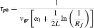
(2.5) ![]()
where vgr is the group velocity (cf. Section 1.3.6). It is not possible to adjust the values of Γtv, αi, and Rf in such a way to keep all four figures constant while simultaneously increasing the cavity length L to improve the thermal rollover power. Instead, g and ηd are kept fixed and τph (constant photon lifetime scaling approach) or Pr (constant power ratio scaling approach) are adjusted (Harder, 2008). The rules for constant photon lifetime scaling are
where L > L0 is the longer cavity length. In this approach, higher power can be obtained by cleaving longer cavities from the same material and reducing Rf according to Equation (2.6) but still maintain the same value for ηd. However, Pr also becomes larger with increasing L, which facilitates the longitudinal spatial hole burning effect. This drawback can be mitigated by using a slightly flared active waveguide (Guermache et al., 2005).
The rules for constant power ratio scaling are
(2.7) ![]()
In this approach, which is the preferred one for long cavities, also Rf is constant, and hence this scaling type is also called constant mirror reflectivity scaling. Both Γtv and αi have to be reduced linearly with increasing L, which is considered a demanding task in the design and fabrication of the vertical structure. The constant power ratio scaling approach has the additional advantage that it makes parameters such as the average optical power in the active layer, drive current density, heat generation density, and spectral stability independent of the cavity length (Harder, 2008).
2.1.3 Transverse vertical waveguides
2.1.3.1 Substrate
The effects of substrate orientation on the quality of epitaxial material and laser performance have already been mentioned in Section 1.4.1. These effects are dependent on the materials used and will be discussed in more detail in the following.
Usually the substrates used for devices have a (100)-oriented surface. Some examples will be given on the effects of misorientation from the exact (100) orientation by some degrees. Chand et al. (1994) observed that by misorienting (100) GaAs substrates toward 〈111〉A by 3 to 4° the incorporation of impurities like oxygen is reduced in AlGaAs, and the AlGaAs/GaAs heterointerfaces are smoother and sharper. Similar positive results were found in AlGaAs lasers grown on GaAs substrates oriented 2° toward the 〈110〉 direction, which led to a reduction of loop dislocations formed at the interface between the substrate and first epitaxial layer (Epperlein et al., 2000, unpublished).
In general, slight substrate misorientations and lower defect densities result in improved laser performances and lifetimes. These results were confirmed by Chen et al. (1987) who demonstrated that similarly tilted substrates led to improved optical quality and lower threshold current densities in (Al)GaAs quantum well (QW) lasers grown on GaAs substrates. More importantly, the surface morphology of the growth on misoriented (100) substrates, and hence threshold current density, is less sensitive to deviations from optimum growth conditions than in (100) substrates, which makes it easier to grow low threshold current material. According to the authors, these enhanced results can be ascribed in part to the fact that misoriented surfaces have steps terminated with Ga. As atoms incident on the surface can then form three bonds, two to the Ga atoms on the (100) surface and one to the Ga atom on the (111) face of the step. This leads to an increased sticking probability of As resulting in smoother AlGaAs layer surfaces. A second mechanism may contribute, because stepped surfaces minimize energetic instabilities at the growth surface (Rode et al., 1977).
The effects of substrate misorientation on material quality and laser performance in other material systems are more diverse. Thus, Mawst et al. (1995) report low-temperature photoluminescence measurements on InGaAs/InGaAsP QW structures showing narrow linewidths for growth on exact (100) GaAs substrates. In contrast, growth on (100) substrates misoriented 2 to 10° off toward 〈110〉 and 10° toward 〈111〉A exhibits broadened luminescence shifted toward longer wavelengths, which can be attributed to interfacial roughness and composition variations due to step bunching growth.
Step bunching refers to the phenomenon where a regular array of monosteps can become unstable and breaks up into regions with high step density or with little or no steps. It has been observed on many surfaces such as vicinal (100) GaAs with surface normals slightly misoriented from specific crystallographic directions resulting in a lowering of the vicinal surface energy by the formation of terraces, steps, or kinks. Several kinetic and thermodynamic mechanisms have been proposed for the formation of step bunching. This includes an asymmetry in the attachment–detachment kinetics of growth units at the step edges, and impurity-induced step bunching where a flux of impurities impinging on the growth surface hampers the motion of a following step, leading to a pinning of steps by impurities (Hata et al., 1998; Cermelli and Jabbour, 2007; Kasu and Kobayashi, 1995).
Corresponding strained-layer InGaAs (active layer)/InGaAsP (confining layer)/InGaP (cladding layer) QW laser structures grown on exact (100) or misoriented substrates show no significant differences in threshold current densities, differential external quantum efficiencies, internal quantum efficiencies, and transparency current densities. However, significant differences are observed in the temperature characteristics with dramatically reduced temperature dependence of Ith and ηd for devices grown on exact (100) substrates compared to structures grown on misoriented substrates. This can be explained by the fact that at high temperatures carrier leakage and hence free-carrier absorption in the confinement layers is more pronounced for 2 to 10° off than for 0° off lasers, because of interfacial imperfections caused by the step bunching effect (Mawst et al., 1995).
By contrast, record-high characteristic temperatures of T0 = 115 K and Tη = 285 K for Ith and ηd, respectively, are obtained by growing compressively-strained InGaAsP/InGaAlP/InGaAlP QW laser structures on (100) GaAs substrates misoriented 10° toward 〈111〉A (Al-Muhanna et al., 1998a). These high values reflect the strong carrier confinement, which is critical for achieving high cw optical power. One reason for this is that the growth on highly misoriented substrates completely disorders InGa(Al)P, which increases the bandgap by about 70 meV (McKenan et al., 1988). This further increases the high bandgap energy of the InGaAlP confining and cladding layers, which even further reduces carrier leakage from the QW. An additional result of the growth on misoriented substrates is that the p-doping is enhanced, which also improves carrier confinement. Surprisingly, other parameters, such as αi, ηi, Jtr, and Γtvg are unaffected by the substrate misorientation, which may be due to an increased roughness in misoriented devices, but the effect is overwhelmed by the large decrease in carrier leakage resulting from the disordered materials (Al-Muhanna et al., 1998a).
2.1.3.2 Layer sequence
Figure 2.1 shows a typical, suitable vertical epitaxial structure in its simplest form for high-power operation, with the InGaAs/AlGaAs QW system as a representative example, and which can be considered as generic for all other diode laser layer structures. Here, we do not discuss device-specific details in the QW structure, confinement region, and cladding layers, as well as relevant modifications in the confinement and cladding regions for tailoring the fast-axis beam divergence angle with keeping the threshold current unchanged and maximizing the output power. These specially designed structures will be discussed in the subsections below.
Figure 2.1 Typical schematic vertical laser design of a strained-layer graded-index separate-confinement heterostructure (GRIN-SCH) quantum well (QW) structure for high-power and low threshold current density operation with a weak optical confinement. The triangular GRIN-SCH shape can be replaced by a more efficient carrier-confining parabolic GRIN-SCH. AlGaAs/GaAs superlattices (not shown) are positioned at specific locations throughout the structure to getter segregating surface impurities, trap diffusing ions at heterojunction interfaces, block threading dislocations, or just serve as useful markers to determine layer thicknesses. Monolayer (ML) thick GaAs spacer layers are sufficient to trap detrimental surface-riding oxygen impurities. Not to scale.

The layer sequence includes a thin GaAs buffer layer on top of the substrate surface, first cladding grading, n-AlGaAs cladding layer, AlGaAs GRIN-SCH layer with embedded InGaAs QW, p-AlGaAs cladding layer, second cladding grading, and p+-contact layer. The buffer layer is meant to isolate the active device layer from the substrate, block any threading dislocations and impurity defects from the substrate, and minimize the loop dislocation density at the substrate/epitaxial layer interface by appropriate initial growth conditions. As already discussed in Section 1.4.1.3, several different short AlGaAs/GaAs superlattices (not shown in Figure 2.1) are positioned at specific locations throughout the structure, each with its own purpose, such as to getter segregating surface impurities, to trap diffusing ions at heterojunction interfaces, to block threading dislocations, or just to serve as a useful marker in scanning electron microscopy (SEM) investigations to determine layer thicknesses.
Abrupt interfaces might cause potential spikes that could lead to unintentional conduction band barriers and additional series resistance. Therefore, to avoid this, interfaces between AlGaAs layers with significantly different Al content are graded over a distance of some nanometers. In molecular beam epitaxy (MBE), this could be achieved by ramping the Al cell over some temperature range, though this might be difficult to control due to the large thermal mass of the effusion cell. Alternatively, mechanical shutters (pulsed material supply) or separate Al cells could be used to control the Al flux, or the linear Al grading could be achieved by trading off the effects of source flux and increased Ga desorption as the substrate temperature increases. In organometallic vapour-phase epitaxy (OMVPE), the grading can simply be achieved by ramping the flux of the Al or Ga precursor. In material systems, such as InGaAs/InP or GaAs/GaInP, where the group-V component changes at an interface, the growth is less well controlled and may lead to detrimental effects including the buildup of strain at the graded interface and the formation of parasitic QWs, which can lead to lasing wavelengths different from the designed ones.
2.1.3.3 Materials; layer doping; graded-index layer doping
Materials
Common compounds for semiconductor lasers have been already discussed extensively in Section 1.1.5. In this subsection we concentrate on materials for high-power diode lasers that are nearly exclusively based on material systems grown on GaAs substrates with layer structures using binary, ternary, or quaternary materials from the (AlGaIn)(AsP) compound group. GaAs-based laser devices dominate the market for high-power diode laser products. However, we will also give a brief account of the commercially important InP- and GaN-based materials and laser devices.
Strained InGaAs QWs are usually embedded in AlGaAs/AlGaAs waveguide structures to cover the wavelength range of 880 to 1060 nm and can achieve high optical output powers (Mikulla et al., 1999; Matuschek et al., 2006; Sebastian et al., 2007). Strain-compensating GaAsP spacer layers have been successfully employed for wavelengths >1000 nm (Bugge et al., 1998). Record-high, single-mode cw powers in the 980 nm wavelength band have been achieved from InGaAs/AlGaAs GRIN-SCH SQW narrow ridge lasers with up to 1.75 W thermal rollover power at 25 °C heat sink temperature and fundamental spatial mode operation in excess of 1.4 W. These devices operate free of catastrophic optical mirror damage (COMD) at maximum power densities above 100 MW/cm2 (Lichtenstein et al., 2004). Yang et al. (2004) achieved >900 mW cw kink-free power for similar devices with high power and current levels at COMD of 1200 mW cw and 1600 mA, respectively, obtained for a low fast-axis beam divergence angle of 13°. By inserting two low-index AlGaAs layers (high AlAs mole fraction) between the waveguide and cladding layer (see Section 2.1.3.5) the far-field could be tuned and fast-axis beam divergence angles in the range of 13 to 24° have been achieved leading to COMD levels between ~1200 and 1000 mW cw, respectively.
High-power Al-free diode lasers emitting in the wavelength range >940 nm have been successfully demonstrated by combining InGaAs QWs with InGaP/InGaAsP waveguides (Botez, 1999a; Al-Muhanna et al., 1998b; Zhang et al., 1993); these devices are also commercially available. The use of the Al-free InGaAs/InGaAsP/InGaP material system has apparently several advantages over the Al-containing InGaAs/GaAs/AlGaAs material system for the realization of reliable, high-power diode laser sources, as follows:
- Lower device series resistance.
- Higher electrical and thermal conductivity compared to AlGaAs (Diaz et al., 1994).
- Lower surface oxidation of InGaP compared to AlGaAs greatly facilitates regrowth for the fabrication of single-mode index-guided structures (Groves et al., 1989).
- Lower facet degradation due to the lower surface recombination velocity of InGaP compared to AlGaAs (Wang et al., 1994; Olson et al., 1989).
Further advantages will be discussed as appropriate within the context of relevant topics in the following sections and chapters.
COMD-free output powers of 430 mW cw and 200 mW fundamental transverse mode powers have been obtained from Al-free 980 nm InGaAs/InGaAsP/InGaP triple-QW (TQW)-SCH ridge lasers 4 μm wide (Asonen et al., 1994). Moreover, internal optical power densities at COMD of typically 18 MW/cm2 cw have been derived from measurements on aperture devices 100 μm wide (Botez, 1999b; Al-Muhanna et al., 1998b). Apparently, there exists no evidence as yet for any clear improvement in output power and COMD performance of 980 nm Al-free lasers compared to that of 980 nm Al-containing lasers, in spite of the fact that appropriate measures also had been taken to expand the mode in the transverse vertical direction (see Section 2.1.3.5 for a description of diverse established techniques).
By adding Al to the InGaAs active region, high-power, strained AlGaInAs/AlGaAs QW lasers can be realized with emission wavelengths in the range down to 731 nm covering also the important 808 nm wavelength for pumping Nd:YAG (Emanuel et al., 1997; Hanke et al., 1999). The presence of indium in the active layer increases the resistance of the material to dark-line defect (DLD) formation (see Chapter 3) and propagation, and hence improves the optical strength and reliability of these diode laser types (Roberts et al., 1998).
AlGaInAs lasers 100 μm wide with high AlAs mole fraction of 0.24 in the active QW yielded COMD power levels of 2.2 W corresponding to a power density of ~8 MW/cm2 (Emanuel et al., 1997), which is only lower by a factor of ~2 compared to Al-free lasers (see above). Furthermore, 40 W cw laser bars 1 cm wide comprising 25 groups of AlGaInAs double-QW (DQW) lasers 200 μm wide emitting in the 808 nm band showed low degradation rates of 10−6 per hour over 3.3×10⁵ accumulated device hours in accelerated life tests (Hanke et al., 1999). The devices showed high slope efficiencies of 1.2 W/A, very low series resistances of 2.2 mΩ, and low internal optical losses of 1.7 cm−1. These results demonstrate that Al-containing lasers can also have the very high reliability usually claimed for Al-free lasers (see also 980 nm high-power lasers above). In conclusion, the fundamental question of whether Al-free lasers are significantly more reliable than Al-containing lasers is still open.
High-power unstrained GaAs/AlGaAs QW lasers are available with emission wavelengths of 800 to 850 nm, although 808 nm devices (Oeda et al., 1998) require very thin QWs with only about 10 to 12 monolayer thicknesses, which is a challenge to control. The wavelength can be further lowered by using AlGaAs QWs and high-power operation of 0.45 W has been demonstrated down to 715 nm for uncoated 12×5 μm stripe AlGaAs QW GRIN-SCH gain-guided lasers (Tihanyi et al., 1994). Maximum cw powers in the 808 nm band of 2.9 and 2.6 W have been obtained for GaAs/AlGaAs SQW-SCH and AlGaAs/AlGaAs SQW-SCH lasers 150 μm wide, respectively. These devices operate without failure at 45 °C, 1 W automatic power controlled (APC) over 2000 h (Shigihara et al., 1991). Al in the active layer leads to strong corrosion and oxidation effects at the laser facets, and hence reduces the power level at the COMD significantly, with the consequence that these lasers possess only a very limited reliability (Yellen et al., 1993).
Quaternary InGaAsP QWs sandwiched in GaInP/InGaAsP waveguide structures offer completely Al-free lasers emitting in the range of 730 to 875 nm with high power and reliability. Uncoated devices 100 μm wide and 700 μm long emitting at 808 nm have achieved maximum COMD-free powers of 5 W cw and long-term reliability without failures at 60 °C, 1 W APC over 3×10⁴ h aging tests (Diaz et al., 1997). High-power emission has also been reported for 808 nm, Al-free active layer InGaAsP lasers with GaInP confinement layers and AlGaAs cladding layers (Hayakawa, 1999). In addition, GaInP/AlGaInP waveguides provide higher barriers and hence lasers down to 700 nm emission wavelengths can be realized (Al-Muhanna et al., 1998a; Mawst et al., 1999). The wavelength range of 715 to 810 nm can also be covered by high-power tensile-strained GaAsP/AlGaAs QW lasers showing high efficiencies and good reliability. AR/HR-coated devices 100 μm wide and 4 mm long showed cw powers of 1.8, 3, and 6.4 W at 718, 735, and 785 nm wavelengths, respectively. The output power is COMD limited and power densities of 2.4, 3.7, and 7.1 MW/cm2, respectively, have been achieved (Erbert et al., 1999).
For the visible wavelength range of 650 to 690 nm, usually compressively-strained GaInP QWs embedded in AlGaInP confinement and AlGaInP cladding layers are used, while tensile-strained GaInP QWs are employed for shorter wavelengths down to 630 nm. High-power operation of lasers emitting in the red wavelength band have been reported (Orsila et al., 1999). Particularly high COMD-free cw powers have been obtained by Watanabe et al. (1994) from devices with thin undoped (Al0.7Ga0.3)0.5In0.5P window layers grown by low-pressure MOCVD (see Section 4.3 for nonabsorbing mirror approaches) on the cleaved facets of MBE-grown strained SQW AlGaInP ridge lasers 4 μm wide and 1200 μm long emitting with a wavelength of 680 nm. A COMD-free maximum optical output power of 300 mW cw, only limited by thermal rollover, has been obtained, which is about twice as much as that of a conventional laser without the window layer, where the power was limited by COMD. The threshold current of ~100 mA and slope efficiency of ~0.75 W/A were the same as those of the conventional laser, which indicates that the window layer does not affect the laser properties. Slow-axis and fast-axis far-field measurements up to 150 mW confirm the fundamental transverse mode operation. This technique applied to AlGaInP lasers appears to be promising considering that these lasers are very susceptible to facet degradation at high power (Watanabe et al., 1994). Miyashita et al. (2000) achieved 121 mW cw for 900 μm long and narrow devices equipped also with a window–mirror structure but emitting in the shorter wavelength band of 659 nm. These authors showed good reliability of lasers 900 μm long emitting at 687 nm at 40 °C and 120 mW APC over 1800 h without failure.
In the short-wavelength regime, diode lasers usually suffer from low efficiencies, which are mainly due to the low conduction band offsets. This can be counteracted by placing superlattices in the upper waveguide structure that act as Bragg reflectors for the electrons and hence reduce carrier escape. The drawback, however, is an increase in the series resistance caused by the additional heterointerfaces. In general, the series resistance is a special issue in (Al)GaInP lasers due to the limitations on p-doping levels (see the next section).
In the blue–UV wavelength regime, great strides have been made in the fabrication of high-power, reliable, GaN-based diode lasers. For a long time effective technological progress was hampered by the mismatch in lattice constants and thermal conductivities between nitride layers and substrates. A recent breakthrough has been achieved by using a triple In0.07Ga0.93N/In0.01Ga0.99N QW structure sandwiched in a GaN SCH and AlGaN claddings, which were deposited on an n-type GaN substrate. Ridge waveguide lasers, 7 μm wide, 600 μm long, and with cleaved uncoated facets, emitted with high efficiency at room temperature record-high cw output powers up to 2 W at wavelengths of 405 nm and operating currents and voltages up to 1 A and 5.7 V, respectively (Saito et al., 2008). Commercial 405 nm blue–violet diode lasers operating in single mode and quasi-continuous wave (q-cw) power of 400 mW are available (Sony Shiroishi Semiconductor Inc., 2010).
Finally, we discuss material systems used for high-power diode lasers emitting with longer wavelengths >1 μm. In1−xGaxAsyP1−y grown on InP substrate is the classical material system delivering wavelengths for long-distance fiber optics communications in the range of 1.1 to 1.65 μm by changing the mole fractions x and y accordingly. Wavelengths at 1.3 and 1.55 μm are of particular interest where the standard silica fiber has minima in total dispersion and loss, respectively. A range of lattice-matched quaternaries extending from InP to the InGaAs ternary line can be grown by complying with the mole fraction condition x = 0.4y+0.067y2 (see Figure 1.11). Direct bandgap energies can be achieved ranging from 0.75 eV for the ternary endpoint In0.53Ga0.47As to 1.35 eV for InP. Compared to AlGaAs/GaAs, the band offsets in this system are quite different: only 40% of the band offset is in the conduction band, whereas the band offset in the valence band of 60% is much higher (Piprek et al., 2000). Further drawbacks include high series resistance, intervalence band absorption, Auger losses, and above all a strong temperature sensitivity of threshold current and efficiency. Internal losses could be reduced to 3 cm−1 by using an asymmetric waveguide structure (Nagashima et al., 2004), but, nevertheless, multiple quantum wells (MQWs) are required to provide sufficient modal gain to get control of the internal losses.
Thus, up to 5 W cw output power have been achieved from compressively-strained InGaAsP/InP MQW SCH lasers 100 μm wide emitting at around 1500 nm (Garbuzov et al., 1996). Record-high 1.2 W cw ex-facet power levels have been obtained from junction-side down-mounted, single-mode ridge lasers 3–5 μm wide and 3 mm long with InGaAsP compounds of different compositions used for the compressively strained QWs, barriers, and confinement, and with InP for the claddings. These lasers emitting in the 14xx nm band are suitable for pumping Raman amplifiers. Usually several 14xx nm individual diode lasers with different wavelengths form a Raman gain block to establish a flat gain over a wavelength range of ~70 nm, which is suitable for wavelength time division, multiplexed Raman pumping applications (Garbuzov et al., 2003).
In the 1.3 μm wavelength range, the material system of strained AlxGayIn1−x−yAs/InP QW has been developed as a potential alternative to the conventional GaxIn1−xAsyP1−y/InP material system (Zah et al., 1994). The former has a higher electron confinement energy and therefore prevents carrier overflow under high-temperature operation. Strained-layer QWs are chosen to reduce the transparency current and the carrier-dependent loss due to the intervalence band absorption. Both 1.3 μm compressively-strained 5-QW lasers and tensile-strained 3-QW lasers were fabricated using a ridge waveguide structure 3 μm wide. In spite of the Al-containing active layer, no COMD was observed at 25 °C up to 218 mW and 103 mW cw for these lasers, respectively. Specifically, the compressively-strained devices showed excellent temperature characteristics with a threshold current characteristic temperature T0 ~ 105 K, which is about twice as high as that for conventional InGaAsP/InP lasers. For operating the compressively-strained lasers at 85 °C with >5 mW cw, a mean-time-to-failure of 9.4 years has been projected from preliminary life tests. These lasers are interesting for uncooled laser applications, such as fiber-in-the-loop (FITL), where the cost of the laser is an important factor.
There is an approach to extend GaAs-based lasers (the long-wavelength limit for InGaAs QWs is around 1.2 μm) with all their positive characteristics, including high-temperature operation (high T0), to 1.3 μm and replace InGaAsP lasers with their thermal problems (low thermal conductivity, high electron escape due to low conduction band offset). This has been achieved by InGaAsN/GaAs QW structures with the incorporation of only a very low N content of <2% to avoid a strong degradation of luminescence efficiency at higher concentrations (Kondow et al., 1996, 1997). This material system (see also Section 1.1.5) now holds all the advantages of the GaAs system with access to the commercially important wavelength range of ~1.2 to 1.3 μm, for example, for direct pumping of Raman amplifiers. Excellent laser characteristics have been reported including threshold current densities down to 500 A/cm2 from narrow-stripe (~4 μm) devices 350 μm long with lasing wavelengths between 1.24 and 1.3 μm and reliable cw operation up to at least 100 °C with high characteristic temperatures T0 of 110 K (Borchert et al., 2000; Riechert et al., 2000). The latter is caused by the high confinement energy for electrons in these structures, which is due to (i) the high conduction band offset of about 80% and (ii) the increased electron mass compared to InGaAs (Hetterich et al., 2000; Shan et al., 1999). The higher electron mass, however, leads to transparency current densities roughly three times higher than for 980 nm InGaAs QW lasers. The highest known optical powers obtained in the InGaAsN material system are 8 W cw from AR/HR-coated, 1.3 μm InGaAsN SQW diode laser devices 100 μm wide (Livshits et al., 2000).
Layer doping
Some essential laser design parameters depend sensitively on both the doping profile in the vertical structure and doping levels in the individual epitaxial layers, and these include the location of the p–n junction relative to the active layer, the series resistance, in particular in the p-type layers, and the optical losses due to free-carrier absorption. An effective design and control of the doping characteristics is therefore vital to achieve high-power laser operation with low threshold current density.
Layer doping – n-type doping
Silicon is the most common n-type dopant in MBE and MOCVD for all III–V compound semiconductors including (Al)GaAs, (Al)GaInP, and InGaAsP. Doping levels up to 5×1018 cm−3 in GaAs can be obtained; above this level the amphoteric nature of Si leads to self-compensation. This means the incorporation of Si not only on Ga sites, but also on As sites or as interstitials. InP-based materials and InGaAs can easily be doped electrically active up to 1019 cm−3 levels.
Layer doping – p-type doping
Beryllium is the most common p-type dopant in MBE for all III–V compounds. Compared to Zn and Mg, Be has some advantages including a smaller diffusion coefficient, which enables better growth control of the required doping profiles and a lower vapor pressure, which decreases the risk of memory effects. Zn supplied by organic precursors, such as dimethyl- or diethyl-Zn, is the preferred p-dopant for MOCVD-grown GaAs and InP-based materials. There are drawbacks with Zn, which include its high diffusion coefficient and re-evaporation tendency. These drawbacks affect the doping profile and incorporation efficiency, respectively, and can be dealt with by optimizing the growth process, usually by reducing the growth temperature and compromising on the material quality. Alternatively, C is a potential p-dopant with a favorably low diffusion coefficient and high incorporation efficiency up to very high levels >1019 cm−3. It can be introduced intrinsically by controlling the growth temperature and V/III ratio or by additional external sources such as trimethyl-As, CCl4, or CBr4. The second approach offers more independent control of doping and intrinsic defects compared to the first approach. By growing at low temperatures <600 °C and V/III ratios ![]() 1, doping levels of 1019 cm−3 can be achieved, a value that can be lowered by growing at higher temperatures reducing also the uptake of oxygen, an impurity, which can form nonradiative recombination centers, particularly in AlGaAs.
1, doping levels of 1019 cm−3 can be achieved, a value that can be lowered by growing at higher temperatures reducing also the uptake of oxygen, an impurity, which can form nonradiative recombination centers, particularly in AlGaAs.
Graded-index layer doping
This issue is discussed by means of a GaAs/AlGaAs GRIN-SCH QW laser structure. During growth at ≥700 °C Be diffuses from the p-type AlGaAs cladding through the entire p-side GRIN into the QW and beyond into the n-side GRIN where it piles up near the Si dopants close to the edge of the n-AlGaAs cladding with the consequence that the p–n junction is displaced from the QW active region. This is the case when the GRIN-SCH region is nominally undoped. The displacement of the p–n junction is significantly reduced when the p- and n-sides of the GRIN regions are doped with Be and Si, respectively (Chand et al., 1994). Detailed investigations showed that Be diffusion is retarded in the n-GRIN and enhanced in the p-GRIN layer (Swaminathan et al., 1992). Thus, the best option is to dope the n-side of the GRIN with Si and leave the p-side of the GRIN region nominally undoped. The Be atoms will diffuse anyway from the cladding into the p-side of the GRIN region. The Si doping starts high in the n-cladding to keep the series resistance low and is gradually decreased in the GRIN toward the active layer to minimize optical absorption losses. On the p-side the grading is steeper and absolute doping levels are higher to compensate for the lower hole mobilities. The thickness of the inner undoped region is optimized with respect to trading off Ohmic and optical losses. The overall doping profile has to be adjusted to achieve the required mode size.
2.1.3.4 Active layer
Integrity – spacer layers
In an InGaAs/AlGaAs system, there are actually two reasons for growing thin GaAs spacer layers between the active InGaAs layer and the AlGaAs GRIN-SCH regions. First, model experiments on AlGaAs/GaAs structures have shown that Be-doped AlGaAs layers tend to have a higher oxygen content than Si-doped ones, which occurs without any contribution from the Be source itself (Chand et al., 1994). Detailed secondary ion mass spectrometry (SIMS) measurements showed a surface segregation of oxygen atoms in AlGaAs and their subsequent trapping at the AlGaAs/GaAs inverted heterointerfaces. Monolayer-thick GaAs is sufficient to trap the surface-riding oxygen impurities. A similar oxygen accumulation effect occurs in InGaAs/AlGaAs structures and without GaAs spacers the laser performance would be degraded strongly (Choi and Wang, 1990; Chand et al., 1991). GaAs spacers physically separate oxygen atoms from the active InGaAs QW. Second, AlGaAs is grown at high temperatures ![]() 720 °C, which leads to Ga losses due to desorption from the surface during growth interruption, usually initiated prior to the growth of the InGaAs QW, which occurs at a much lower temperature
720 °C, which leads to Ga losses due to desorption from the surface during growth interruption, usually initiated prior to the growth of the InGaAs QW, which occurs at a much lower temperature ![]() 510 °C (cf. Section 1.4.1). Deposition of thin GaAs layers prior to the growth interruption compensates for the anticipated Ga desorption losses.
510 °C (cf. Section 1.4.1). Deposition of thin GaAs layers prior to the growth interruption compensates for the anticipated Ga desorption losses.
Integrity – prelayers
Strong extrinsic impurity-related luminescent emissions have been observed in low-temperature (2 K) photoluminescence (PL) spectroscopy measurements on nominally undoped GaAs/AlGaAs MQW structures with different well thicknesses (Epperlein and Meier, 1990). The intensity of these extrinsic PL emissions is strongest in the first GaAs QW grown in the MQW structure and depends sensitively on the thickness of the preceding AlGaAs barrier layer. Measurement of the binding energies of the involved impurities and excitation power dependence of the spectra revealed that the extrinsic PL is due to the radiative recombination of free electrons in the n = 1 quantized state of the well with neutral carbon acceptors. It is known that the solubility of impurities in AlGaAs is lower than in GaAs and hence impurities remain afloat on the AlGaAs growth surface and are progressively trapped in a thin layer at the inverted interface (GaAs on AlGaAs) upon deposition of the GaAs. This may lead to interface roughness and the formation of defects due to the growth-inhibiting nature of carbon, for example, by preventing the lateral propagation of the atomic layers because of pinning steps on the surface. These extended and point defects have a negative impact on the performance and reliability of a diode laser. Quantitative measurements showed that carbon-related PL can be suppressed to a low level <0.5% of the intrinsic (impurity-free) PL by a GaAs SQW 5 nm thick grown before the actual, measuring QW. By applying this scheme to a QW diode laser an improved device performance can be expected. In Section 7.2, we will resume the impurity gettering issue and discuss it in more detail.
Integrity – deep levels
Deep-level-transient spectroscopy (DLTS) measurements on MBE-grown GaAs/AlGaAs SQW structures have yielded a series of known electron traps located in the upper AlGaAs layer close to the QW interface within a region of about 15 nm (As et al., 1988). The formation of these traps is due to a growth temperature which is far below the optimum temperature of ![]() 720 °C when ramping up the temperature from the ideal low temperature of
720 °C when ramping up the temperature from the ideal low temperature of ![]() 580 °C for the GaAs growth. It is known that the concentration of each of these traps doubles every 50 °C below 720 °C. The time to stabilize to the optimum temperature of 720 °C is equal to the time to grow by about 25 nm, which agrees well with the observed full width at half maximum (FWHM) of the trap distributions. The growth temperature for the lower AlGaAs cladding layer was at its optimum value throughout the growth and hence no traps have been observed. These traps may impact the performance of AlGaAs diode lasers due to higher internal losses and may also be responsible for enhanced degradation processes. An interrupted growth after the QW may allow the resumption of optimum AlGaAs growth conditions, therefore preventing the formation of these performance-deteriorating defect states. In Section 7.3, we will discuss the experimental details further including the DLTS technique.
580 °C for the GaAs growth. It is known that the concentration of each of these traps doubles every 50 °C below 720 °C. The time to stabilize to the optimum temperature of 720 °C is equal to the time to grow by about 25 nm, which agrees well with the observed full width at half maximum (FWHM) of the trap distributions. The growth temperature for the lower AlGaAs cladding layer was at its optimum value throughout the growth and hence no traps have been observed. These traps may impact the performance of AlGaAs diode lasers due to higher internal losses and may also be responsible for enhanced degradation processes. An interrupted growth after the QW may allow the resumption of optimum AlGaAs growth conditions, therefore preventing the formation of these performance-deteriorating defect states. In Section 7.3, we will discuss the experimental details further including the DLTS technique.
Quantum wells versus quantum dots
Today's semiconductor diode laser products are exclusively based on QW active layer concepts and technologies. In principle, this includes all diode laser types, such as narrow-stripe and wide-aperture emitters, and one- and two-dimensional arrays, practically for all commercial applications. This dominance is determined by several factors:
- Impressive performance based on the unique QW strengths, particularly those of strained QW structures, as discussed in Chapter 1.
- Successful exploitation of the fundamental physical parameters into effective, reliable, and reproducible technological concepts, and focused optimizations of the QW/waveguide structures targeted at achieving high gain characteristics, low carrier and photon losses, temperature-stable characteristics, and fit-for-purpose beam divergence angles.
- Utmost reliability figures and extremely long diode laser product lifetimes of greater than 30 years.
In the ultimate case of size quantization realized in a quantum dot (QD), which includes a narrow energy-gap material embedded in a wide-gap matrix, carriers are confined in all three dimensions for QD sizes in the order of the exciton Bohr radius. Energy levels of the carriers are then discrete and separated, and the density of states narrows to delta function-like distributions. QD lasers with these atomic-like density of states are expected to have major advantages over QW lasers, including:
- lower threshold current densities;
- higher temperature stability of characteristics with infinitely high characteristic temperatures T0 and Tη;
- higher differential gain and tunability of gain spectrum; and
- lower chirp, that is, lower shift of the lasing wavelength with injection current.
Despite the promising potential of QD systems, the best results, obtained to date after nearly three decades from the theoretical inception of QD lasers (Arakawa and Sakaki, 1982) and two decades since the first report on self-assembled QDs (Ledentsov et al., 1994), do not match the high-power performance of commercial QW lasers.
The fabrication of QDs is based on a well-accepted approach by using a Stranski–Krastanow (1937) growth mode, where highly strained semiconductors are epitaxially grown on lattice-mismatched substrates with the formation of coherently strained islands after a few monolayers of growth. Elastic strain relaxation and renormalization of the surface energy are the driving forces for this self-assembled growth process (Bhattacharya et al., 2004). The islands can be subsequently buried to form the QD. The main drawbacks of this in-situ fabrication technique are its high cost and the low control over shape, size, material composition, and positioning of individual dots.
Nevertheless, QD lasers with low threshold and high modulation speed have been realized. However, their temperature stability and narrow linewidth have fallen far short of expectations. This is due to the dispersion of the QD size, shape, composition, and local strain, which leads to an inhomogeneous broadening of the excited state transitions and hence broadening of the ideal gain spectrum. Inhomogeneous line broadening is responsible for the parasitic recombination of carriers residing not in the QDs but primarily in the surrounding optical confinement layer at higher temperatures. These significant hot-carrier effects and associated gain compression are due to a density of states that is far less in the QDs than in the surrounding layers. Additional parasitic recombination currents can be caused by the thermal population of nonlasing QDs and by pumping nonlasing QDs through the inhomogeneous line broadening effect (Asryan and Luryi, 2001, 2002).
In summary, we can conclude that low carrier collection efficiency in the active layer, the various carrier loss processes, as well as thermal broadening of holes in the valence band of QDs, impact the performance of QD lasers by deteriorating the maximum gain, threshold current density, characteristic temperature coefficients T0 and Tη, internal efficiency, and optical output power.
Several approaches have been proposed to mitigate these negative effects and which include the following:
- Generation of high-density and uniform QDs by optimizing growth parameters, using seeding layers (Mi and Bhattacharya, 2005) or patterned substrates (Kiravittaya et al., 2006).
- Use of a QW tunnel injection structure, first demonstrated in QW lasers and then in QD lasers for reducing hot-carrier effects (Bhattacharya et al., 1998; Bhattacharya, 2000). Here, the carrier collection efficiency is improved by the QW and subsequent phonon-assisted resonant tunnel injection of cooled electrons into the QD. Theoretical considerations have predicted that parasitic recombination of carriers outside the QD can be reduced considerably and large values for T0 > 1500 K could be obtained by using tunnel injection. Further enhancement of T0 results from the resonant nature of tunneling injection by selectively cutting off the nonlasing QDs (Asryan and Luryi, 2001, 2002).
- Modulation p-doping of the QD barrier. Holes of the p-doped barrier are then transferred into the hole ground state of lower energy in the adjacent QD layer. Therefore, fewer electron–hole pairs are required to be injected from the contacts to compensate for the thermal broadening of the hole distribution. This increase of the hole ground state occupancy increases the gain (Fathpour et al., 2005; Liu et al., 2007).
- Use of short-period (GaAs)6(AlAs)6 superlattices of indirect bandgap as barrier material for direct bandgap semiconductor QDs (Sun et al., 2004).
- Formation of QDs in the center of a QW, for example, by depositing an InGaAs layer 1.1 nm thick into a GaAs QW layer 10 nm thick surrounded by AlGaAs barriers. This quantum-dots-in-a-well (DWELL) structure minimizes carrier thermal escape from the dot states to barrier levels (Patanè et al., 2000).
Despite the large body of work dealing with QD technology-baselining activities including growth, fabrication, material, and device characterization, relatively very little work has been carried out in diode laser product baselining aimed at achieving high optical output powers, which could be competitive to the state-of-the-art high-power performance of QW lasers. This mismatch is also reflected in the type and number of published data on fundamental and applied QD technology issues. A rigorous search of the published literature in 2009, which includes review articles (not many), textbooks (actually only one), and companies (about two) committed to the development of QD laser products, clearly reveals a disparity between achievements gained on QD technology basic topics and QD diode laser output powers, in stark contrast to the market-leading QW diode laser technology. Certainly, good progress has been made in QD diode laser technology, which includes the following:
- Record-low cw threshold current densities of 19 A/cm2 in 1.3 μm InAs/GaAs lasers (Park et al., 2000).
- High characteristic temperature coefficients T0 ≥ 650 K and Tη = ∞ up to 80 °C in 1.3 μm InAs/InGaAs/GaAs devices 100 μm wide (Mikhrin et al., 2005).
- Record-high small-signal modulation bandwidths of ν−3 dB
 25 GHz measured in 1.1 μm In(Ga)As lasers (Fathpour et al., 2005).
 - Low dynamic chirp of 0.1 Å and zero linewidth enhancement factor α 0 (Mi et al., 2005).
Note: The linewidth enhancement factor describes the spectral behavior associated with carrier density variations in diode lasers, and (1+α2) is a measure for the spectral linewidth broadening. It is defined as α = −2k0(∂nr/∂N)/(∂g/∂N) where nr is the refractive index, g the material gain, N the carrier density, and k0 the vacuum wavenumber (Henry, 1982).
- High differential gain dg/dN 8.5×10⁻¹⁴ cm2 at 283 K in InGaAs/GaAs QD ridge lasers (Bhattacharya and Ghosh, 2002).
However, on the optical output power side, the reported achievements are less numerous than in QW laser technologies and only a few can be considered as competitive with established and commercial QW diode laser products. The following data may illustrate the situation:
- 16 W cw total optical powers measured at both uncoated facets of junction side-down on microchannel heat sink mounted, 1.25 μm InAs/GaAs QD lasers 200 μm wide and 4 mm long (Crump et al., 2007). The laser is fabricated in the most common material system used for QD diode lasers. To the author's knowledge, this power is the highest achieved for any QD diode laser device type. The figure has to be compared to the 8 W cw obtained from AR/HR-coated, 1.29 μm InGaAsN SQW lasers 100 μm wide (Livshits et al., 2000). Both QD and QW lasers deliver about the same output power by taking into account the different laser cavity widths and lengths.
- 250 mW single-mode ex-fiber from InAs/GaAs QD diode lasers emitting at available wavelengths 1064, 1210, 1320 nm (Innolume GmbH, 2008). For comparison, a single-mode fiber-coupled InGaAs/AlGaAs SQW laser delivers 400 mW cw ex-fiber and kink-free at 1070 nm and room temperature (Oclaro Inc., 2010). (Note: ex-fiber power is the power emitted from a fiber-coupled laser).
- 3 W from a tapered InGaAs/GaAs QD laser and 3 W from a broad-area InGaAs/GaAs QD laser 100 μm wide both emitting at 920 nm (Kaiser et al., 2007; Deubert et al., 2005). Comparable QW lasers yield optical powers higher by a factor of 2–3 (cf. Table 1.4) and 7 (cf. Table 1.3), respectively.
- 400 mW cw from a single-mode QD laser emitting in the range of 915 nm and consisting of a single layer of self-assembled InGaAs QDs embedded in a GaAs QW 6 nm wide and processed to a ridge waveguide section 1 mm long followed by a taper 2 mm long with a full angle of 4° (Kaiser et al., 2006). Comparable single transverse lateral mode InGaAs/AlGaAs SQW narrow-stripe single ridge waveguide pump lasers emit up to 1800 mW cw COMD free in the wavelength range 9xx nm and at room temperature (Lichtenstein et al., 2004).
Number of quantum wells
The effects of number of active QWs nqw on laser performance and reliability are manifold and have been thoroughly investigated in many publications. We will summarize here the major effects and results.
In general, lasers with MQWs in the active region have higher differential gain and transverse vertical optical confinement factor, which leads to lower threshold current density, weaker temperature dependence of laser characteristics, and higher characteristic temperature coefficient T0 (Namegaya et al., 1994). However, it may also lead to the generation of misfit dislocations due to the increased total active layer thickness (Namegaya et al., 1994) and stronger facet heating, with the consequence of lower COMD levels (Chapters 7–9; Epperlein, 1997; Epperlein and Bona, 1993). The higher differential gain of MQW lasers leads also to narrower linewidths and higher modulation frequencies due to the greater relaxation oscillation frequency compared to SQW lasers. The last two positive features are more important for high-speed telecommunications than high-power (pump) applications.
The decision to select a SQW or MQW depends on the loss level. In the case of high losses, the MQW is always better because the gain comes from the high-slope part of the modal gain versus current characteristic instead of the saturated part of the SQW gain curve. The MQW has a higher differential gain in the gain versus current dependence. (Note: In a simple approximation, the MQW gain curve is the SQW gain curve multiplied in both axes by the number of wells.) In this case, the saturated gain of the SQW may not always be large enough to reach threshold gain. However, at low loss, the SQW is always better due to both its lower transparency current Jtr (only states of one QW have to be inverted) and its lower internal loss (Γtv,qwαi scales with number of wells) (cf. Sections 1.3.4.3 and 1.3.5.1). The optimum number of QWs depends on the required gain at threshold (Weisbuch and Vinter, 1991; McIlroy et al., 1985).
In Sections 1.3.4.2 and 1.3.4.3, we discussed the influence of the number of wells on the threshold current of a QW laser and its length dependence. For details, we refer to these sections, including Figure 1.22.
Namegaya et al. (1994) have carried out an extensive investigation of the effects of well number nqw on the material and device properties of compressively-strained 1.3 μm Ga0.11In0.89As0.63P0.37/InP GRIN-SCH MQW lasers. The wells are 4 nm thick and the number of wells in the MQW devices is in the range of 4 to 12. In the following, we discuss the major calculated and experimental results.
Low-temperature PL spectroscopy showed an increase in both the PL peak wavelength and FWHM for devices with nqw ≥ 10. In addition, the material with 12 wells showed a strongly reduced PL peak intensity. As has been demonstrated by critical thickness calculations, these PL effects can be ascribed to (i) the total thickness of the wells exceeding the critical thickness for the nqw ≥ 10 samples and (ii) the consequent degradation of the crystal quality due to strain relaxation. From calculations on the influence of device parameters on T0, it is found that small values for αi and αm and large values for nqw, Γtv,qw, and g0 are effective for high-temperature operation of up to 170 °C. T0 increases with increasing well number and facet reflectivities and high values of T0 ![]() 80 K have been obtained for nqw ≥ 6 and operating temperatures up to 100 °C. At room temperature, the minimum threshold current is obtained for nqw = 4, whereas at higher temperatures >150 °C the minimum is at nqw = 8. This is consistent with αi increasing and g0 decreasing with increasing temperature and by using the expression nqw = (αi+αm)/(Γtv,qwg0) for achieving a minimum threshold current derived from the condition that at threshold the modal gain has to balance the total losses (see Section 1.3.4.2; McIlroy et al., 1985).
80 K have been obtained for nqw ≥ 6 and operating temperatures up to 100 °C. At room temperature, the minimum threshold current is obtained for nqw = 4, whereas at higher temperatures >150 °C the minimum is at nqw = 8. This is consistent with αi increasing and g0 decreasing with increasing temperature and by using the expression nqw = (αi+αm)/(Γtv,qwg0) for achieving a minimum threshold current derived from the condition that at threshold the modal gain has to balance the total losses (see Section 1.3.4.2; McIlroy et al., 1985).
The experiments showed also that the internal quantum efficiency ηi is independent of nqw, and the internal losses αi increase with nqw, which can be attributed to the increased volume of the absorptive material and total optical confinement factor Γtv (cf. Section 1.3.4.3). High-power cw emission of >300 mW at 1.3 μm and 730 mA could be achieved at room temperature from optimized single-mode, narrow-stripe, six-QW lasers 1 mm long with low threshold currents of Ith < 13 mA.
Further useful results include the dependence of the FWHM fast-axis beam divergence angle θ⊥ on nqw. θ⊥ increases continuously from ~22° to 32° for nqw = 4 to 10. This gives the opportunity to adjust the fast-axis divergence angle to the slow-axis angle θ‖ in order to achieve a circular output beam, which could make it easier to couple power from narrow-stripe lasers with larger θ‖ angles into single-mode fibers. Moreover, accelerated life tests showed that elastically strained-layer MQW lasers with 8 and 10 wells exhibit a significantly higher degradation rate >10% of the threshold current than corresponding lattice-matched MQW devices. Critical thickness calculations clearly showed that this degradation is caused by a degradation of crystal quality suffering from critical thickness. Devices with 4 and 6 wells are free from inelastic, plastic strain relaxation and dislocation formation effects, whereas devices with more than 8 wells are unstable. Finally, it should be noted that the latter effect can be compensated by using a strain-compensating scheme.
In strained-layer MQW structures the net strain is accumulated, which means that the allowable strain in a SQW is reduced. By using strain-compensating barrier layers with a strain, which is opposite to that in the well layer, each well is then exposed to a similar accumulated strain originating from the underlying layer. This approach can also be applied to generate high strain levels in a SQW with the goal to extend the wavelength range, for example, by using GaAsP barriers in highly strained InGaAs/GaAs QW lasers the lasing wavelength could be extended to 1060 nm (Bugge et al., 1998). Strain-compensated lasers also show a higher reliability because of the reduced driving force for strain-activated defect generation. Another positive effect of strained barriers could include the adjustment of the band structure to enhance the performance of certain diode lasers. In this way, the use of tensile-strained GaAlInP barriers in red-emitting lasers could improve the carrier confinement, reduce the absorption of laser light at the mirror facet, and thus enhance the optical strength of the laser (Valster et al., 1997).
2.1.3.5 Fast-axis beam divergence engineering
The beam divergence property is of great importance whenever laser power is required to be coupled efficiently into another device enabling high-power, high-brightness applications including pumping fiber amplifiers, optical storage, and direct material processing. The requirement is not only for high output power but also for narrow beam divergence. Conventional GRIN-SCH QW structures with their tight optical confinement in the transverse vertical (fast-axis) direction usually yield large divergence angles θ⊥ > 30°. However, this results in highly asymmetric elliptical far-field patterns with high aspect ratios >3.5, which require sophisticated optical systems to achieve acceptable coupling efficiencies (cf. Section 1.4.3.3). Tuning the composition of the cladding and GRIN-SCH layers or reducing their thicknesses can lower θ⊥ to ≈ 25° in InGaAs/AlGaAs lasers, but at the expense of lower kink-free powers and efficiencies and higher threshold currents; θ⊥ decreases at a rate of ![]() 1° per 1% AlAs mole fraction reduction in these lasers.
1° per 1% AlAs mole fraction reduction in these lasers.
Expanding the optical mode in the transverse vertical direction is now a proven and powerful concept to reduce strongly the divergence angle with the additional advantages of:
- maintaining the low threshold current;
- lower risk of COMD failures at high-power operation;
- single-mode operation and suppression of higher order mode lasing; and
- suppression of beam filamentation effects.
There are many different approaches to realize this concept, each with its own pros and cons. In the following, we try to categorize the different approaches and discuss the major technologies.
Thin waveguides
By thinning the active waveguide layer much below the thickness used in conventional designs, the fast-axis divergence angle can be strongly reduced and the maximum output power limited by COD increased. Narrow-stripe (Al)GaAs lasers with thin active waveguides of only ![]() 0.04 μm thickness, which is typically about five times less than in conventional lasers, yield θ⊥
0.04 μm thickness, which is typically about five times less than in conventional lasers, yield θ⊥ ![]() 16° and P
16° and P ![]() 200 mW (Hamada et al., 1985). However, the strong spreading of the mode far into the cladding layers leads to significant free-carrier absorption resulting in an increase of threshold current and decrease in differential external quantum efficiency. This drawback can be mitigated by the so-called thin tapered-thickness approach where the active waveguide is thicker in the bulk of the laser cavity than near the mirrors. In this way, the fast-axis divergence angle and threshold current can be controlled independently and values of 10° and 60 mA, respectively, from (Al)GaAs devices 3.5 μm wide have been obtained (Murakami et al., 1987). Another approach includes an asymmetrically expanded optical mode toward the substrate side by increasing the refractive index of the n-cladding layer relative to that of the p-cladding. This design can furnish low divergence angles θ⊥
200 mW (Hamada et al., 1985). However, the strong spreading of the mode far into the cladding layers leads to significant free-carrier absorption resulting in an increase of threshold current and decrease in differential external quantum efficiency. This drawback can be mitigated by the so-called thin tapered-thickness approach where the active waveguide is thicker in the bulk of the laser cavity than near the mirrors. In this way, the fast-axis divergence angle and threshold current can be controlled independently and values of 10° and 60 mA, respectively, from (Al)GaAs devices 3.5 μm wide have been obtained (Murakami et al., 1987). Another approach includes an asymmetrically expanded optical mode toward the substrate side by increasing the refractive index of the n-cladding layer relative to that of the p-cladding. This design can furnish low divergence angles θ⊥ ![]() 23°, θ‖
23°, θ‖ ![]() 9°, low threshold currents Ith
9°, low threshold currents Ith ![]() 40 mA, and high kink-free powers of 600 mW from 980 nm strained InGaAs/AlGaAs DQW lasers 3.5 μm wide and 1500 μm long (Shigihara et al., 2002).
40 mA, and high kink-free powers of 600 mW from 980 nm strained InGaAs/AlGaAs DQW lasers 3.5 μm wide and 1500 μm long (Shigihara et al., 2002).
The above experimental values for θ⊥ can be confirmed to a good approximation with values calculated on the basis of the formula (cf. Equation 1.43) discussed in Section 1.3.5.3. In general, lasers based on the thin-waveguide structure approach may be sensitive to instabilities, which could be caused by the weak localization of the mode, refractive index changes due to current injection, and variations in the fabrication processes.
Broad waveguides and decoupled confinement heterostructures
Broad-waveguide (BW) SCH lasers have been developed primarily to achieve high cw power levels by providing concomitantly both a large equivalent transverse vertical mode spot size d/Γtv as well as low internal cavity losses αi ≤ 1 cm−1 with no sacrifice in wall-plug efficiency at high drive current levels; here d is the active layer thickness and Γtv the transverse vertical confinement factor. From the definition of the internal optical power density at COMD, ![]() , Botez (1999b) derived an expression for the maximum cw power
, Botez (1999b) derived an expression for the maximum cw power
(2.8) ![]()
where W is the stripe width and Rf the front-facet reflectivity. One way to increase d/Γtv is to use a BW-SCH structure by expanding the fundamental mode through increasing the SCH guiding layer thickness tc. The SCH layer with index nr,w is sandwiched between cladding layers which have an index nr,cl < nr,w. Accurate analytical approximations for d/Γtv and θ⊥ have been given by Botez (1999b) as
(2.9) ![]()
where w0 is the equivalent near-field Gaussian waist
(2.11) ![]()
and D is the normalized waveguide thickness defined as
(2.12) ![]()
and where nr,w and nr,cl are the refractive indices of the waveguide layer and cladding layer, respectively, λ is the vacuum wavelength, and nr,w > nr,cl.
For large d/Γtv ![]() 0.66 μm values, 0.97 μm emitting InGaAs/InGaAs(P)/GaAs BW-SCH QW lasers 100 μm wide and 2 mm long with high values for Tη
0.66 μm values, 0.97 μm emitting InGaAs/InGaAs(P)/GaAs BW-SCH QW lasers 100 μm wide and 2 mm long with high values for Tη ![]() 1800 K and ηd > 85%, high cw power levels of 11 W and low fast-axis divergence angles θ⊥
1800 K and ηd > 85%, high cw power levels of 11 W and low fast-axis divergence angles θ⊥ ![]() 22° could be obtained. These devices are designed for tc
22° could be obtained. These devices are designed for tc ![]() 1 μm, which is lower than the cutoff thickness for the second-order mode. The experimental θ⊥ data are in excellent agreement with calculations based on Equation (2.10). Further decrease of θ⊥ can be obtained by decreasing the index step, Δnr = nr,w − nr,cl, which is consistent with the thin-waveguide concept discussed in the previous subsection.
1 μm, which is lower than the cutoff thickness for the second-order mode. The experimental θ⊥ data are in excellent agreement with calculations based on Equation (2.10). Further decrease of θ⊥ can be obtained by decreasing the index step, Δnr = nr,w − nr,cl, which is consistent with the thin-waveguide concept discussed in the previous subsection.
A major problem with the BW concept is that low divergence angles and high powers with low-risk COD failures can be obtained, but at the expense of the excitation of higher order transverse vertical modes at high injection currents.
In the context of the BW-SCH approach, we want to discuss the decoupled confinement heterostructure (DCH) concept (Hausser et al., 1993). In the DCH design, the electronic and optical confinements are decoupled by an internal barrier, and hence both can be optimized independently. It is characterized by a broadened waveguide and thin carrier block layers sandwiching the active region. These barrier layers have to be thick enough to prevent carrier leakage, while being as thin as possible (<40 nm) so as not to appreciably affect the optical waveguiding. Crucial for a proper operation of the barriers is that they are highly n(p)-type doped on the n(p)-side of the junction with typically 3×1018 cm−3. Thus, these highly doped thin barrier layers pose no obstacle to majority carrier injection into the active layer, and they act as efficient barriers for the minority carriers in order to prevent carrier leakage. Undoped barrier layers not only lead to carrier leakage of minority carriers, but also inhibit an efficient injection of majority carriers.
Numerical simulations have shown that the leakage currents depend sensitively on barrier width, barrier doping, and barrier material. The simulations showed that hole (electron) leakage in an InGaAsP/InP DCH laser system can be suppressed to ~1% (14%), which compares to ~24% (27%) in a symmetric SCH structure (Hausser et al., 1993). The smaller improvement in electron leakage may be due to the fact that the thin barrier layers are less efficient for electrons due to their much lower mass compared to that of holes. The suppression of carrier leakage in DCH lasers leads to lower internal optical losses and an increase in the characteristic temperature T0.
By lowering the confinement factor Γtv, and in combination with the reduced optical losses, the hole burning effect and hence filamentation can be suppressed (see Section 2.2.1.6). This leads to more stable single-mode lasers with higher single-mode power operation. In addition, the DCH structure allows lowering of the Al content in the waveguide and cladding layers of Al-based lasers compared to SCH lasers. The effect results in less laser heating, improved power conversion efficiency, and higher reliability due to a lower electrical and thermal resistivity. Thus, optimized InGaAs/AlGaAs SQW DCH lasers have delivered 9.5 W cw for devices 100 μm wide (thermal rollover limited). Narrow devices with buried ridge waveguides 4–6 μm wide emitted up to 1.3 W cw thermal rollover power and 0.7 W cw single transverse lateral mode, kink-free power in FWHM beam divergence angles of 20° and 8° in the fast-axis and slow-axis directions, respectively (Yamada et al., 1999).
Low refractive index mode puller layers
The intensity profile of the optical mode is engineered by manipulating the spatial variation of the refractive index of the cladding layers in such a way as to achieve both small beam divergence and low threshold current. This is realized by implementing a lower refractive index layer between the GRIN-SCH confinement and cladding layer on both sides of the waveguide.
The design principle is to maximize the mode intensity in the center of the active layer to achieve low threshold currents and to expand the optical field outside into the claddings to achieve small beam divergence angles (Yen and Lee, 1996a). The optical mode in the GRIN-SCH QW region is tightly confined, whereas outside of the low-index layers the mode spreads because the lasing mode index is reduced by the two low-index layers to be close to the index of the claddings.
This effect is illustrated in Figure 2.2 by comparing the calculated near-field profile of the new structure to that of the conventional one in InGaAs/AlGaAs GRIN-SCH QW devices; the calculations have been carried out by using the commercial simulation package LASTIP (Crosslight Software Inc., 2009). The corresponding experimental transverse vertical far-field profiles (Figure 2.3) show a reduction of θ⊥ from 32° to 19° for these nonoptimized InGaAs/AlGaAs lasers, which also showed no change in the threshold current (Epperlein et al., 2000, unpublished).
Figure 2.2 Simplified illustration of a transverse vertical InGaAs/AlGaAs GRIN-SCH QW waveguide structure without (dashed line) and with (solid line) low refractive index (high AlAs mole fraction) layers in the cladding layers on both sides of a conventional optical confinement GRIN-SCH layer. Calculated near-field (NF) profiles for the structure without (dashed line) and with (solid line) low-index layers.

Figure 2.3 Experimental transverse vertical far-field (VFF) profiles for a conventional InGaAs/AlGaAs GRIN-SCH QW diode laser without (dashed line) and with (solid line) low-index layers (high AlAs mole fraction 0.5) in the cladding layers. Gaussian fit (dotted line) to the VFF profile with low-index layers.

In general, θ⊥ decreases with increasing Al content (corresponds to decreasing index) and thickness of the AlGaAs mode puller layers, and with decreasing Al content in the AlGaAs claddings. The reason is clear that as the cladding index increases to be closer to the lasing mode index, the lasing mode becomes more expanded leading to a smaller θ⊥ and increased Ith. Further decreasing the Al content of the claddings is critical since the cladding index can exceed the fundamental mode index. As a result, there is no guided mode in the waveguide (Lin et al., 1996).
Moreover, simulations show that the requirements on the growth conditions are very tight with an Al content to be controlled better than 2% in order to hit θ⊥ to within 10% of the target value. Anyway, record-low far-field angles of 13° have been reported on optimized 980 nm InGaAs/AlGaAs ridge waveguide lasers 4 μm wide and 3 mm long with low threshold currents of 66 mA, high slope efficiencies of 0.88 W/A, and single-mode operation up to very high powers of 1200 mW cw (Lin et al., 1996; Yang et al., 2004).
Optical traps and asymmetric waveguide structures
The purpose of the optical trap and asymmetric waveguide is to expand the mode toward the n-side of the structure and restrict its spread in the p-doped region, which minimizes the series resistance and free-carrier losses and leads to low fast-axis divergence angles and threshold currents, high differential quantum efficiencies and high kink-free powers, and suppression of higher order modes at high drive currents. Optical traps can be realized in different ways:
- Make the index profile of the confinement layer (such as LOC, which is the large optical cavity version of a SCH) asymmetric by increasing the index on the n-side (Peters et al., 2005; Li et al., 2008; Shigihara et al., 2002).
- Place a large optical superlattice between the confinement layer and n-cladding (Lichtenstein et al., 2006).
- Insert a graded higher index layer with a ∧-shaped profile (∨-shaped dip of Al content for AlGaAs) and well-defined thickness in the n-cladding at an optimized position far away from the active layer (Qiu et al., 2005).
Experimental results from the latter approach include low fast-axis angles of 18°, low threshold currents of 30 mA, single-mode output powers of 400 mW, and strong suppression or even elimination of higher order modes achieved in narrow ridge waveguide InGaAs/AlGaAs QW lasers. Additional positive effects of this approach are that the incorporation of the optical trap has no adverse impact on threshold current and slope efficiency. The optical trap layer constitutes essentially a much weaker waveguide compared to the waveguide in the active region. To retain single-lobed near-field distribution and hence avoid side lobes in the far field, its thickness has to be optimized. There is also an optimum range of separation between the active layer and the optical trap layer for low fast-axis beam divergence. Moreover, this optical trap approach offers the freedom to design independently the vertical far-field and optical overlap with the active layer and in addition leads to a significantly improved growth tolerance.
An improved suppression of higher order lateral modes can also be achieved within the first approach in the list above by using a layer structure that supports an optical mode asymmetrically expanded toward the substrate into the n-cladding layer of a ridge structure (Shigihara et al., 2002). We will discuss this approach in more detail in Section 2.2.1.2. Furthermore, an asymmetric waveguide, which expands the mode toward the n-side of the waveguide structure, has proven to be very efficient in improving free-carrier losses, optical losses, differential efficiency, internal efficiency, and series resistance. Thus, the highest reported power conversion efficiencies (see Equation 1.53) of 75% have been achieved to date on 808 nm InGaAlAs/AlGaAs broad-area lasers 100 μm wide and 1 mm long (Li et al., 2008). These lasers with ultralow series resistances of 0.07 Ω, high slope efficiencies of 1.4 W/A, and low threshold current densities of 180 A/cm2 emit >5 W cw in smooth single-lobed far-field patterns with 32° and 8° for the fast-axis and slow-axis beam divergence angles, respectively.
Spread index or passive waveguides
The insertion of passive waveguides with increased refractive index in the cladding layers offers another opportunity to stretch the optical mode in the transverse vertical direction and thus decrease the beam divergence. This coupled waveguide structure, also called spread index (SPIN) structure (Lopata et al., 1996), is composed of an active waveguide, which provides gain and two passive waveguides to modify the far-field pattern.
Figure 2.4 shows the calculated transverse vertical near-field and far-field profiles of a standard InGaAs/AlGaAs structure with and without GaAs layers placed into both the cladding layers for comparison, and demonstrates an effective reduction of the fast-axis divergence angle by 9° down to 16° (Epperlein et al., 2000, unpublished).
Figure 2.4 Refractive index and calculated transverse vertical near-field (NF) and far-field (FF) profiles of an InGaAs/AlGaAs GRIN-SCH QW laser structure: (a) conventional structure; (b) conventional active waveguide structure with two passive waveguides (with increased index) to expand the near-field and shrink the far-field pattern.
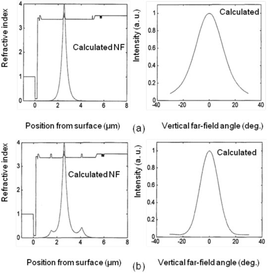
The parameters, which affect the mode profile, are the thickness and distance of the high-index GaAs layers from the active waveguide. Since the field distribution is at maximum in the active QW region, relatively low threshold currents of 24 mA and high slope efficiencies of 0.9 W/A can be expected from SPIN InGaAs/AlGaAs QW lasers exhibiting low fast-axis divergence angles of 17° (Lopata et al., 1996). Further experimental fast-axis divergence angles include even lower values of 15° (Ziari et al., 1995) and 11° (Chen et al., 1990) for similar lasers.
Coupled mode theory and exact numerical calculations (Yen and Lee, 1996b) require that the thicknesses of the passive waveguides are thinner than a critical thickness for the fundamental mode operation. In addition, the separation between waveguides needs to be large enough and the coupling strong enough to effectively modify the far-field distribution. Side lobes can appear in the far-field pattern if the separation between waveguides is too large, which should be avoided. Optimization of the compositional and geometrical parameters of the individual building blocks of the coupled waveguide structure is complex in order to achieve single-mode operation at low thresholds and low fast-axis divergence angles over a wider acceptable parameter range.
An alternative approach utilizes periodic index separate confinement heterostructure (PINSCH) layers as optical confinement to simultaneously reduce the transverse vertical beam divergence and increase the maximum output power (Wu et al., 1991). InGaAs/AlGaAs PINSCH QW lasers with ridge waveguides 5 μm wide and 750 μm long show good performance, which includes θ⊥ ![]() 20°, Ith
20°, Ith ![]() 45 mA, ηd
45 mA, ηd ![]() 90%, and single-mode cw powers >620 mW.
90%, and single-mode cw powers >620 mW.
Leaky waveguides
Although the leaky waveguide approach (Streifer et al., 1976) has no relevance in commercial laser products, we briefly describe here its basic functionality and essential features by means of the GaAs/AlGaAs system. A thin AlGaAs layer with lower refractive index is placed between the higher index, active GaAs gain region and the GaAs substrate. Thus, optical power can flow through the thin AlGaAs layer and leak into the substrate, which occurs preferentially for higher order modes due to their higher penetration depth. The optical mode experiences only minor absorption losses in the substrate and escapes upon refraction from the cleaved facet into a well-collimated beam with a low divergence angle of only a couple of degrees. There are some drawbacks linked to this approach, which include
- high threshold current densities for high leaking losses;
- significant contribution of lasing in the active waveguide for a weak leaking process; and
- strong laser power losses in the contact layer/electrode layer in case the angle of the leaking modes is too high.
Spot-size converters
Spot-size converter integrated laser diodes are key components for reducing the fabrication cost of optical transmitter modules. They can provide low-loss direct coupling to the optical fiber or silica waveguide without the need for a lens. In addition, they offer expanded tolerance for optical alignment, mode stability, and narrow beam divergence by expanding the near-field fundamental mode. Several types of spot-size converters have been developed to expand the smaller, asymmetrical mode shape of a laser diode to match the larger circular mode of a single-mode fiber (cf. Section 1.4.3.3). These can be categorized into two groups: laterally tapered (Vawter et al., 1997; Bissessur et al., 1998) and vertically tapered waveguides (Kobayashi et al., 1997; Aoki et al. 1997) integrated with the active waveguide of the laser. In these lasers, the optical mode is highly confined in the gain region to generate sufficient optical gain, whereas it is expanded in the converter region in both the lateral and vertical directions.
The schematic structure of a Fabry–Pérot laser monolithically integrated with a tapered waveguide thickness spot-size converter is shown in Figure 2.5a. An example of a laterally tapered active waveguide configuration is exhibited in Figure 2.5b. In this so-called double-core taper structure power is transferred from the tapered active ridge waveguide to the underlying passive coupling waveguide.
Figure 2.5 Schematic representation of two spot-size converter structures to expand the optical mode size: (a) monolithically integrated (vertically) tapered thickness of active waveguide; (b) laterally tapered active waveguide with underlying coupling passive waveguide (double-core structure).

An effective lateral taper requires tapering the active waveguide width typically from 2 to 0.5 μm over a length of 1 mm. The shape of the taper can be linear over the entire length or in subsections with different taper angles. Adiabatic transformation supplies the best results, but requires a nonlinear taper, which can be approximated by an exponential shape. Fabrication usually implies a single epitaxial growth step, conventional projection lithography, and wet or dry etching. More advanced processing includes electron beam direct write and highly anisotropic chlorine reactive ion beam etching (RIBE) to produce the taper, including the narrow tip with high surface quality and shape fidelity. Considerably expanded near-field spots have been achieved, which translate into very narrow far-field patterns with very low divergence angles of θ⊥ ![]() 7° and θ‖
7° and θ‖ ![]() 6° forming a nearly circular laser beam (Vawter et al., 1997).
6° forming a nearly circular laser beam (Vawter et al., 1997).
In the vertical taper approach, calculations show that a thickness ratio of the taper of at least 3 must be achieved over a length of typically 200 μm to have efficient fiber coupling and low radiation loss (Kobayashi et al., 1997). In this case, the near-field spot is expanded to about 2.5 μm. There are several techniques for fabricating in-plane thickness modulation, which include selective area growth (SAG) on dielectric masked substrates (Kitamura et al., 1999; Kasukawa et al., 1997; Hirose et al., 1999), selective area etching (Brenner et al., 1995) and shadow-masked growth (Demeester et al., 1990; Aoki et al., 1997). In SAG, the growth rate in a narrow-stripe spacing depends on the width of the patterned SiO2 masks surrounding the stripe on the substrate. The growth rate decreases with decreasing mask width resulting in thinner layers. Thus, a gradual change of layer thicknesses in the taper and a sufficient coupling between the tapered region and gain region can be achieved. In addition, this technique enables the growth of a smooth core layer that is free from any harmful scattering sites in the laser resonator.
An important advantage of the thickness tapering approach is that the converter region is transparent to the laser light because the thinner active QW layers shift the absorption edge to shorter wavelengths. Experimentally it is found that for achieving the required thickness ratio of 3 requires a mask width of 30 μm for the active layer, which narrows gradually down to 4 μm toward the end of the taper. In this way, a virtually flat area 300 μm long for the gain region and a thickness reducing area 200 μm long with a thickness ratio of 3 for the tapered waveguide can be grown simultaneously (Kobayashi et al., 1997). SAG has the additional advantages of precise dimension control, high uniformity and reproducibility, simultaneous growth of layers with different thicknesses and compositions, control of the bandgap energy of a MQW structure and etching-free process for waveguide formation. The lowest transverse vertical divergence angle achieved with this approach is 9° (Kobayashi et al., 1997). Due to the strong expansion of the near-field mode pattern, COMD-related degradation problems at the laser facets can be practically excluded.
Photonic bandgap crystal
Photonic crystals (Yablonovitch, 1987; Joannopoulos et al., 1995) are composed of periodic dielectric nanostructures affecting the propagation of photons in the same way as the periodic potential in a semiconductor crystal determines the motion of electrons and holes by generating allowed and forbidden electronic energy bands.
Essentially, photonic crystals contain multidimensional structures with a periodic modulation of the refractive index. Photons will pass through regions of high index interspersed with regions of low index. To a photon, the contrast of refractive index looks just like the periodic potential that a charge carrier experiences when moving through the semiconductor crystal. For a large contrast in refractive index, there is a formation of allowed bands in photon energy separated by forbidden regions, the so-called photonic bandgaps. Since the wavelength of the photons is inversely proportional to their energy, the photonic crystal will block light with wavelengths in the photonic bandgap, while allowing other wavelengths to propagate freely throughout the crystal. This gives rise to distinct optical phenomena such as inhibition of spontaneous emission, highly selective optical filters, high-reflecting omnidirectional mirrors, and low-loss waveguides.
Since the basic physical phenomenon is based on diffraction, the periodicity of the photonic crystal structure has to be of the same length scale as half the photon wavelength, which poses high demands on the fabrication of high-quality photonic bandgap crystals (PBCs) operating in the visible part of the spectrum.
For edge-emitting diode lasers a waveguide based on a longitudinal PBC (LPBC) has been developed to realize stable high-power single-mode lasing with a very large modal spot size leading to narrow beam divergence, increased COMD threshold, single-mode operation in broader devices, and suppressed beam filamentation (Maximov et al., 2008). In a LPBC, light propagates in a medium with a refractive index regularly modulated in the direction perpendicular to the propagation axis, which is qualitatively analogous to the operation of a photonic crystal fiber. The basic structure of a LPBC consists of a periodic sequence of layers with alternating high and low refractive index and a localizing optical defect violating the periodic index profile.
Basic types of optical defects are, for example, to increase the index or thickness of one high-index layer compared to the other high-index layers in the periodic sequence. The strength of the defect, which determines the number of optical modes localized by the defect, is then in these cases proportional to the difference in the index and thickness. To achieve single fundamental mode lasing the strength of the optical defect in the LPBC has to be designed in such a way that only the fundamental optical mode is localized by the defect and decays away from the defect, whereas the higher order modes are extended over the entire LPBC.
The general LPBC concept for laser application employs a LPBC on the n-side where the gain region containing the active QWs forms a localizing optical defect due to the high refractive index of these wells. An increase in the number of periods results both in a stronger discrimination of higher order modes by a decrease in the confinement factors of these modes and in a narrowing of the fast-axis divergence angle. Single-mode operation requires strong discrimination between the fundamental mode and the higher order modes in either modal gain and/or loss, which can be realized in different ways:
- Design the confinement factor of the fundamental mode to be much larger than that of the higher order modes.
- Realize a leaky design where all extended higher order modes penetrate into the (absorbing) substrate and contact layer (dependent on laser wavelength), whereas the localized fundamental mode has a very low leaky loss.
- Introduce additional absorbing layers into the structure affecting only all extended modes but not the localized fundamental mode (Maximov et al., 2008).
Even in the case of large leakage losses for all higher order modes, but with confinement factors smaller for the fundamental mode than for the higher order modes, single-mode operation with narrow fast-axis beam divergence can be obtained. By modifying some layers close to the substrate, the preferential leakage of higher order modes can be effectively controlled.
For example, by making the high-index layer closest to the substrate thicker and the low-index layer closest to the substrate thinner by a factor of 2 leads to a substantial leakage of higher order modes into the substrate with the fundamental mode practically unaffected, which finally results in a relative increase of higher order mode losses by about a factor of 10. Together with a larger confinement factor for the fundamental mode, single-mode operation with narrow fast-axis beam emission can be achieved (Maximov et al., 2008).
Figure 2.6 shows the vertical waveguide structure of a typical LPBC laser, considering only the LPBC specific layers (Maximov et al., 2005). High-performance LPBC edge-emitting FP lasers in different material systems have been achieved and include the following:
- GaInP/AlGaInP lasers, 4 μm wide and 1.5 mm long, emit at 658 nm in single-mode with 115 mW cw power into a narrow fast-axis beam divergence angle θ⊥ 8° and with a characteristic temperature T0 155 K.
- GaAs/AlGaAs lasers, 4 μm wide and 1 mm long, emit at 850 nm in single-mode 270 mW cw into a far-field pattern of θ⊥ 9° and θ‖ 5° with an external differential quantum efficiency ηd 87%.
- InGaAs/AlGaAs lasers, 10 μm wide, 1.5 mm long, and with a threshold current of 200 mA, emit at 980 nm in single-mode 1.2 W cw into a narrow far-field pattern with angles θ⊥ 4° and θ‖ 3.5°. The 10 μm wide devices showed single transverse lateral mode operation up to high pump currents, which demonstrates the potential of the LPBC structure for single lateral mode operation in wider stripe lasers (Maximov et al., 2008).
Figure 2.6 Schematic cross-section of the vertical structure of an edge-emitting Fabry–Pérot (FP) diode laser employing a longitudinal photonic bandgap crystal (LPBC) waveguide configuration together with a double quantum well (DQW) as optical defect for single-mode and narrow-beam operation. (Data adapted in amended form from Table I in Maximov et al., 2005.)

2.1.3.6 Stability of the fundamental transverse vertical mode
A major problem with some of the approaches discussed in the preceding section for expanding the optical mode is that low beam divergence angles and high COMD power levels may be obtained but at the expense of the excitation of higher order transverse vertical modes at high injection currents. This is particularly the case for approaches based on conventional waveguides such as broad waveguides or mode puller schemes employing the insertion of low refractive index layers or passive waveguide layers into the claddings on both sides of the gain-generating active region.
If the modal spot size or more precisely the equivalent transverse spot size d/Γtv exceeds a critical value, the effective waveguide width (thickness) may exceed the cutoff thicknesses for higher order mode excitations and the differences in the optical confinement factor between fundamental and higher order modes become very small. According to Botez (1999b), this can occur for 970 nm InGaAs/InGaAsP/InGaP BW structures with d/Γtv ![]() 0.42, 0.58, and 0.75 μm, leading to effective waveguide widths (thicknesses) of
0.42, 0.58, and 0.75 μm, leading to effective waveguide widths (thicknesses) of ![]() 0.53, 1.1, and 1.58 μm, which correspond to the cutoff thickness for first-, second-, and third-order mode excitation, respectively.
0.53, 1.1, and 1.58 μm, which correspond to the cutoff thickness for first-, second-, and third-order mode excitation, respectively.
In addition, the power reflectivity of higher order modes is larger than that of the fundamental mode (Casey and Panish, 1978). Consequently, at relatively thin waveguide thicknesses ![]() 0.5 μm multiple transverse vertical mode operation may degrade the far-field pattern and cause kinks in the P/I characteristics due to mode switching effects.
0.5 μm multiple transverse vertical mode operation may degrade the far-field pattern and cause kinks in the P/I characteristics due to mode switching effects.
Another drawback with these approaches may originate from the high sensitivity of the field confinement at the large spot sizes to minor changes in the refractive index caused by current injection as well as compositional and temperature instabilities.
Altogether, it appears that these approaches enable only in a very limited design and operational space a reliable and robust laser operation with a stable optical mode. Similar limitations may also be true for the thin waveguide structure approach. Spot-size converters, however, may be very effective in achieving the lowest far-field divergence patterns of 7°×6° with nearly circular beam shapes, but impose great requirements on the design and fabrication of tapered waveguides to achieve the highest possible transformation of the optical mode and power in a reliable and reproducible way.
In the LPBC approach, the mode localization strength depends sensitively on the thickness and refractive index of the core layer comprising the active QW structure and forming the actual optical defect feature. Any variation of the defect thickness may change the localization of the fundamental mode and hence the confinement strength relative to that for higher order modes. However, even for up to 30% variations in the defect thickness, the leakage of higher order modes remains much larger and therefore continues to provide single-mode lasing and low fast-axis beam divergence of typically 8° for the fundamental mode. In principle, the LPBC approach enables the design of ultrabroad waveguides in a very robust way, which includes the insensitivity to variations over a wider range of active region thicknesses and refractive indices.
Finally, it has been demonstrated experimentally that the LPBC laser design is capable of delivering single lateral mode cw powers of up to 3 W from stripe lasers 10–20 μm wide emitted into a low transverse lateral far-field angle of ![]() 2° (Maximov et al., 2005).
2° (Maximov et al., 2005).
2.1.4 Narrow-stripe weakly index-guided transverse lateral waveguides
2.1.4.1 Ridge waveguide
In Chapter 1, we discussed a weakly index-guiding approach realized in rib and ridge waveguide types of lasers. Common to these designs is that the thickness of at least one layer is laterally nonuniform. In both types of scheme, the lateral laser structure can be modified such that an effective refractive index step of <10−2 is generated under the rib or ridge zone. This index step is larger than the carrier-induced index suppression leading then to a relatively stable index-guiding of the lateral mode. In rib lasers, the thickness, for example, of the waveguide layer or the active layer, can be varied laterally. However, current spreading in the p-cladding layer can affect the threshold current density.
In ridge lasers, where the ridge is formed in the upper p-cladding by etching and embedded in a dielectric layer, the loss of effective current by current spreading is less pronounced. However, carrier diffusion in the active layer, which extends beyond the ridge, affects the threshold current, but also produces a continuous lateral variation of gain and index. The partial overlap of the mode with the dielectric layer forms an effective index step with a size determined by the height of the ridge and the residual thickness to the active layer, which is the thickness of the remaining p-cladding layer outside the ridge. A sensitive adjustment of the etch depth is required to provide enough effective lateral index step for single lateral mode operation. The beam quality and fundamental mode operation of ridge waveguide lasers are sensitively dependent on the design of critical ridge dimensions and their control during device fabrication. These topics will be discussed in more detail in Section 2.3 below.
Narrow ridge waveguide, single-emitter lasers have been extensively investigated and are widely employed in many key application areas because of their:
- simple fabrication technology requiring only one single epitaxial growth step;
- low optical losses;
- low threshold currents;
- low parasitic capacitances;
- high reliability;
- high control of the lateral index step providing single-mode operation for devices with a wide active region;
- easy integration; and
- record-high optical powers emitted in a single transverse vertical and lateral mode.
2.1.4.2 Quantum well intermixing
Quantum well intermixing (QWI) has proven to be an extremely useful and important technology for patterning in a post-growth process the refractive index and bandgap in the plane of the QW layers, with two principal objectives. First, to obtain high-performance device applications including low-loss lateral waveguides and nonabsorbing mirror structures in diode lasers. Second, to integrate monolithically optical devices such as diode lasers, detectors, modulators, and optical switches in a photonic integrated circuit.
The QWI process can be localized to selected regions of the QW structure so that the optical properties of only the selected areas are modified in this bandgap engineering process. It involves the interdiffusion of constituent atoms across the well/barrier interface resulting in a controlled modification of the material composition, which leads to a change in the bandgap and shift of the absorption edge to higher energies. Figure 2.7a shows a schematic representation of the QWI process.
Figure 2.7 Schematic diagrams of the quantum well intermixing (QWI) process and its application in transverse lateral waveguiding. (a) Simplified conduction and valence band structure of a GaAs/AlGaAs QW before and after QWI. Resulting increase in bandgap energy and decrease in refractive index of the intermixed QW are also indicated. Only group-III atoms Ga and Al are shown. (b) Simplified illustration of a transverse lateral laser waveguiding structure based on QWI by an ion implantation process.
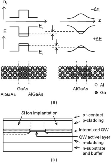
A number of intermixing techniques have been successfully developed and can be categorized as follows:
- Impurity-induced disordering (Laidig et al., 1981) through ion implantation with subsequent high-temperature annealing (Thornton et al., 1985; Welch et al., 1987; Epperlein et al., 1987, unpublished) and without subsequent thermal treatment (Kuttler et al., 1998) or Zn diffusion (Itaya et al., 1996) or ion beam intermixing at elevated temperatures.
- Laser-induced disordering (Epler et al., 1988).
- Impurity-free vacancy disordering (Kowalski et al., 1998), which is based on the generation of group-III vacancies during the deposition of SiO2 capping layers; these vacancies then diffuse through the structure during thermal treatment in a rapid thermal annealer leading to enhanced intermixing and an increase in bandgap energy.
In Chapter 4, we discuss these techniques in detail, in the context of enhancing the optical strength and robustness of diode lasers by developing efficient nonabsorbing mirror concepts.
Here, in this section, we restrict our discussion to the development of lateral waveguide structures by QWI processes. Decisive for this application is that the shift of the bandgap energy and the linked refractive index change are sufficiently high. Blue shifts of the bandgap wavelength can be as high as 60 and 50 nm obtained by impurity-free vacancy disordering of 1.55 μm InGaAs/AlGaInAs MQW structures (Bubke et al., 2002) and ion implantation-induced disordering of 850 nm GaAs/AlGaAs SQW structures (Epperlein et al., 1987, unpublished), respectively. Refractive index reductions of 0.18 (5.2%) have been measured on Zn-disordered 850 nm GaAs/AlGaAs QW lasers (Gray and Marsh, 1996). Such figures have enabled the fabrication of low-threshold, single-mode, real refractive index waveguided, planar buried heterostructure diode lasers using a silicon impurity-induced disordering process (Thornton et al., 1985; Welch et al., 1987). Figure 2.7b shows the schematic cross-section of a QW laser with a transverse lateral waveguide realized by QWI through an ion implantation process. One of the leading high-power, single-mode, single-emitter pump laser products is based on this technology.
2.1.4.3 Weakly index-guided buried stripe
This type of laser structure has the potential to deliver a stable transverse lateral mode, high kink-free output power, high reliability at high power operation, and a reasonable aspect ratio of the far-field pattern. Useful features of this structure are that the thickness of the p-type cladding layer, which significantly affects the transverse lateral mode can be controlled more precisely than that in a ridge waveguide and that the fabrication process is simpler and more reproducible due to the self-alignment involved. Precise design and control of the composition and thickness of the cladding and current blocking layers are essential to realize a low effective refractive index step in the horizontal direction of about 2–5×10⁻³ for a stable transverse lateral mode operation up to high power. Typical buried-stripe widths are between 2.5 and 5 μm (Figure 2.8).
Figure 2.8 Schematic cross-section of a weakly index-guided, self-aligned buried-stripe diode laser depicting the essential components for single transverse lateral mode operation. Cross-sectional scanning electron microscopy image of an InGaAs/AlGaAs QW laser with n-type InGaP current blocking layer.

The fabrication consists of a two-step growth method and standard photolithography, dry and wet selective etching processes. The first epitaxial step includes the following layers: n-buffer, n-cladding, active region with optical confinement, first p-cladding, etch stop, n-current blocking, and possibly a suitable cap layer. The latter is recommended, in case the current blocking layer is of AlGaAs to avoid rapid oxidation of its exposed surface after etching the buried stripe. A thin GaAs cap layer is appropriate, but it must be damage-free to ensure optimum regrowth and also a high reliability of the finished laser device. Equally crucial is that all etched surfaces are free of defects so that a defect-free regrowth of the second p-cladding layer and the top contact layer can be obtained. Figure 2.8 shows a schematic generic cross-section of the structure and a cross-sectional view of a real device (Epperlein et al., 2000, unpublished).
High kink-free powers of 980 nm, strained-layer InGaAs/AlGaAs GRIN-SCH QW lasers have been obtained from buried-stripe types of structures (Figure 2.9): 475 mW cw for 5 μm×1500 μm large devices with InGaP current blocking layers and typical threshold currents of 32 mA (Epperlein et al., 2000, unpublished) and 545 mW for devices 2.2 μm wide and 1000 μm long with AlGaAs current blocking layers and threshold currents around 22 mA (Horie et al., 2000). In both cases, the maximum slope efficiency is ![]() 0.88 W/A. The lower kink-free power level in the former case may be due to the larger buried-stripe width (opening in the current blocking layer) which is more than twice that in the latter case.
0.88 W/A. The lower kink-free power level in the former case may be due to the larger buried-stripe width (opening in the current blocking layer) which is more than twice that in the latter case.
Figure 2.9 Optical output power versus drive current characteristic of a strained-layer, single-mode 980 nm InGaAs/AlGaAs GRIN-SCH QW diode laser with a self-aligned buried-stripe structure and n-type InGaP current blocking layers.

2.1.4.4 Slab-coupled waveguide
The slab-coupled optical rib waveguide laser is a high-power, high-brightness diode laser that emits light in a single spatial, fundamental mode with a nearly circular profile and large modal diameter of several micrometers. The concept of this laser is based on results from a coupled-mode analysis between a rib and a slab region (Marcatili, 1974), and states that by appropriately selecting the slab thickness t, rib height h, and rib width w, the slab region acts as a mode filter and removes higher order modes from the rib region (i.e., these modes are coupled to the continuum of slab modes, which then radiate energy laterally). The criteria for a single-mode rib waveguide are determined by the ratios of effective slab thickness/effective rib height and effective slab thickness/effective rib width where the effective waveguide dimensions are the actual waveguide dimensions increased by the field decay lengths in the adjacent layers (Marcatili, 1974).
This mode filtering scheme allows a much larger mode area and a lower fundamental mode loss than in conventional ridge lasers. The large circular mode area strongly reduces the power density at the facets and therefore reduces significantly the risk for COMD-related laser failures. It also allows butt coupling to single-mode fibers with high coupling efficiency and without the use of lenses. The low modal loss makes possible longer devices, which would have reduced heat dissipation at high-power operation and therefore reduced thermal waveguiding. Gain is added to the rib region by a MQW structure so that the lowest order mode will lase without causing sufficient gain guiding in a higher order mode. Low modal gain implies, however, that the loss in the waveguide must also be kept very small (Donnelly et al., 2003).
The structure is grown in a single epitaxial growth step and the device, schematically shown in Figure 2.10, looks similar to a ridge laser except that the ridge is etched through the active region into the waveguide layer forming the rib region (Donnelly et al., 2003). Defects generated at the etched surfaces could lead to degradation in long-term reliability. Deposition of SiO2 or Al2O3 passivation layers or regrowth of appropriate semiconductor layers in the etched grooves could mitigate these detrimental effects. The thickness of the waveguide layer of typically 4 μm is much larger than that used in standard single-mode lasers, and the height and width of the rib region are larger and nearly the same. The slab thickness is typically in the range of 3 to 3.5 μm. The grooves are etched 30–100 μm wide, and have to be wide enough so that the unpumped regions outside the grooves do not affect the lowest order mode, which is confined in the rib region but narrow enough so that the optical absorption in the unpumped regions can contribute to the loss of the slab-coupled higher order modes, possibly enhancing mode stability. The MQW gain region is placed on top of the waveguide in order to avoid having a waveguide inside a waveguide and having the lowest order mode localized around the MQW region (Donnelly et al., 2003).
Figure 2.10 Schematic cross-section of a generic slab-coupled optical waveguide diode laser structure with a multiple quantum well (MQW) active region placed on top of the thick passive waveguide. The fundamental, bound spatial mode in the rib waveguide is also shown (dashed line). (Adapted in amended form from Donnelly et al., 2003.)

These lasers operating in a large, low aspect ratio, lowest order, single-lobed spatial mode have a large nearly circular near-field spot of typically 4.2 and 3.8 μm, and far-field divergence angles of 11 and 12° in the slow-axis and fast-axis directions, respectively, enabling butt coupling of power with high efficiency up to 88% into a single-mode fiber of 4.2 μm mode diameter. Single-mode 980 nm InGaAs/AlGaAs QW lasers with an optimum length of 1 cm have low internal losses of ~0.8 cm−1, high internal efficiencies close to unity, and high cw output powers >1 W (Donnelly et al., 2003).
2.1.4.5 Anti-resonant reflecting optical waveguide
The lateral structure of the anti-resonant reflecting optical waveguide (ARROW) consists of a low refractive index core region, which defines the lateral spot size of the device, surrounded by highly reflecting, high index cladding layers (Mawst et al., 1992a; Yang et al., 1998). The reflecting cladding layers are designed with a thickness and refractive index that correspond to an odd number of quarter lateral wavelengths λ1/4 of the radiation leakage from the fundamental ARROW mode where λ1 is the lateral wavelength in the high-index, anti-resonant reflecting layers. In this way, the anti-resonant fundamental mode suffers low radiation loss. However, higher order modes, which are not anti-resonant, suffer much higher losses, preventing them from reaching the threshold for lasing.
Typical ARROW structures have a core width between 4 and 6 μm and a built-in lateral index step Δnr > 0.03, which provides mode stability to high output power, strong discrimination against higher order lateral modes, strong stability against gain–spatial hole burning, and which makes the device insensitive to index variations caused by temperature and carrier injection. An additional positive feature of the device is its buried-type structure with a planar top configuration for efficient heat sinking.
Figure 2.11 shows a simplified generic cross-section of a single-core ARROW laser structure along with the lateral index profile. The structure is usually grown by a two-step MOCVD process. The first step is up to the high-index guide layer (to be patterned to the lateral anti-resonant reflectors) and includes the vertical n-cladding, active waveguide structure and a current blocking layer used in the finished so-called self-aligned stripe (SAS) device geometry to restrict current injection to the low-index core region. The ARROW pattern is defined by conventional photolithography and wet chemical etching prior to the second growth step, which includes the thick vertical p-type cladding layer and the p+-doped contact layer. The lateral effective index step is designed such that the reflector regions with typical widths of 0.9 μm are anti-resonant for the fundamental ARROW mode. The injected current is self-aligned to the low-index core region by the current blocking layers (reverse-biased junctions). The thicknesses of these layers are chosen such that the effective refractive index in the regions outside the high-index reflectors is identical to that in the core region (Yang et al., 1998).
Figure 2.11 Schematic cross-section of the generic vertical structure of the anti-resonant reflecting optical waveguide (ARROW) semiconductor diode laser and the transverse lateral effective refractive index profile. (Adapted in amended form from Yang et al., 1998.)
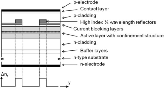
Mode calculations on a 2D ARROW waveguide structure (Yang et al., 1998) show that the dominant mechanism for higher order mode discrimination is lateral edge radiation loss resulting in a low loss of ~2 cm−1 for the fundamental mode and high losses of >16 cm−1 for the higher order modes calculated for a 970 nm InGaAs/InGaAsP laser structure. Such a large difference in edge losses and the immunity to gain–spatial hole burning are essential prerequisites for operating the laser in single spatial mode to high drive currents in excess of 10 times threshold. Calculations also show that the mode discrimination is large over a wide range of effective index step size, which leads to more relaxed fabrication tolerances and hence reproducible device parameters.
Measured far-field patterns show transverse lateral divergence angles as low as 4.5° from core devices 6.5 μm wide in single-mode operation (Yang et al., 1998). The best single-mode output powers of 300 mW cw are from single-core structures 4 μm wide emitting into a narrow transverse lateral far-field pattern with half-width angle θ‖ = 9° (Mawst et al., 1992a).
2.1.4.6 Stability of the fundamental transverse lateral mode
In the preceding sections, we have briefly described the strengths and weaknesses of the various approaches with respect to stable and reproducible operation of diode lasers in the fundamental transverse lateral mode. In this section, we discuss and summarize the major features of each technique relating to this stability issue.
In general, a major challenge for high-power diode lasers is the lateral mode instabilities that arise from the conflicting design requirements for high output power and single transverse lateral mode operation. In the sections above, we have shown that a large optical mode size is required for various reasons to achieve a narrow and preferably circular far-field pattern and to avoid damage to the facets. In the fast-axis direction, the optical confinement is determined by the layer structure, and the waveguide in this direction has to be thin enough to support only the fundamental mode even at high output powers. In the transverse lateral direction, a small refractive index step is required to suppress the higher order modes in the waveguide with a large lateral mode size. In various studies, it has been shown that the coherent superposition of the various transverse lateral modes is responsible for the formation of kinks in the P/I characteristics and far-field beam steering effects (Guthrie et al., 1994; Schemmann et al., 1995). Therefore, to achieve high-power single-mode output, two approaches can be taken to design waveguides either that support only the fundamental lateral mode or that allow higher order lateral modes but with a gain insufficient to reach lasing threshold.
The mode stability of ridge lasers is primarily determined by the waveguide geometry and layer composition where the dominating parameters are the ridge width and residual waveguide thickness in the etched regions outside the ridge. In Section 2.3, we discuss the results of a sensitivity analysis performed on the dependence of the fundamental mode and far-field pattern in the transverse lateral direction on these parameters. These results show a very limited window for fundamental mode operation determined by relatively narrow ranges of ridge widths, residual thicknesses, and slow-axis beam divergence angles for a given vertical laser structure. Proven practical approaches to obtain in the etching process the optimum residual thickness leading to single-mode devices with low threshold current and slow-axis beam divergence angle include applying the ridge etch, first at specific locations of a companion wafer, before applying a beveled etch across the actual laser wafer. This procedure can enhance the yield of fit-for-purpose laser devices.
For a given ridge width, the number of modes supported by a ridge waveguide, and their lasing conditions, depend on both the difference in effective refractive index between the regions within and outside the ridge and the transverse lateral gain distribution which couples to the field. However, this built-in index step can be very different to the actual index profile caused by detrimental effects such as index changes by carrier injection (Xu et al., 1996), local thermal heating, and mechanical stress, resulting in the emergence of higher order lateral modes. For instance, time-dependent measurements on the laser beam quality degradation show that the temperature profile in the cavity plays a significant role in the transverse lateral guiding of the lasing modes (Hunziker and Harder, 1995).
Other approaches affecting the discrimination between the fundamental and higher order modes as well as the threshold current are to reduce the ridge height and p-cladding layer thickness (Wu et al., 1995). In Section 2.2, we describe how, from the point of view of a lateral index step, a low-ridge and thin p-cladding device can be considered as equivalent to a high-ridge, thick p-cladding device and can deliver the same low-index step of ~3×10⁻³ required for stable single-mode operation. In addition, we describe results from numerical studies (Chen et al., 2009) on the lateral mode behavior impacted by effects such as self-heating, spatial hole burning, lateral carrier distribution, and gain profile variation with increasing input current.
Most of the topics discussed above as potential parameters determining the stable fundamental lateral mode operation of ridge waveguide lasers are also valid for planar BH lasers realized by a QWI process, which leads to real refractive index lateral waveguides. This includes parameters such as effective waveguide width and height, p-cladding thickness, and all perturbing contributions with the potential to cause the generation of higher order optical modes as discussed above. The compositional modification in the QW structure, especially in strained material systems, raises the question of QW material quality after the intermixing process, which could give rise to mode instabilities. In general, it has been demonstrated that no degradation in the quality of the QW takes place: for instance, PL spectra show that strained QWs are still coherently strained, and InGaAs/GaAs SQWs disordered by shallow As implantation and thermal annealing show good structural integrity. However, on the other hand, compositional interdiffusion in lattice-matched InGaAs/InP systems can give rise to a strained structure after the QWI process. High-resolution transmission electron microscopy lattice images show no misfit dislocations in these disordered structures and the lasers show no degradation in threshold current.
The weakly index-guided buried-stripe laser has the built-in advantage of maintaining stable fundamental transverse lateral mode operation up to high power even with the occurrence of spatial hole burning. However, the laser device has to be carefully designed and fabricated, requiring a low transverse lateral index step of ~3.5×10⁻³, a narrow buried-stripe width of 2.2 μm, and a defect-free etching of the stripe and optimum regrowth of the upper layers. A novel double etch-stop structure and associated selective etching processes can realize these requirements to maintain the stability of the mode. The geometrical and compositional tolerances acceptable for stable transverse lateral mode operation are not known. One reason for achieving stable mode operation is that in this structure the thickness of the p-type cladding layer outside the buried-stripe region, which significantly affects the transverse lateral mode, can be controlled more precisely than, for example, in a ridge waveguide. In addition, the fabrication process involves a self-alignment process, which supports the geometrical specifications to be met for transverse lateral mode operation. Furthermore, long cavity structures provide better thermal conditions and reduce the effective injected carrier density in the active region, which, in turn, leads to a very stable transverse lateral mode. In addition, the thickness of the cladding layers is 2.2 μm in order to suppress resonant mode coupling between the ordinary mode in the laser waveguide (laser mode) and an unusual mode (substrate mode) propagating in the transparent substrate, which has a larger refractive index than the cladding layers. The thick cladding layers lead to an improved linearity of the P/I characteristic due to the elimination of substrate mode-induced mode hopping. Finally, stable transverse lateral mode operation is also demonstrated in long-term laser stress tests performed at high optical output power and high temperature (Horie et al., 2000).
Slab-coupled waveguide lasers with a large, properly designed passive rib wave-guide support in principle only one bound spatial mode due to coupling of the higher order modes into the slab modes. However, only slight changes in waveguide geometry can lead to mode changes, such as devices with wider ribs (e.g., increase from 4.6 to 5.4 μm) and shallower etch depths have lower lateral index confinements, which can contribute to the emergence of mode instabilities at higher power levels. These instabilities are thermal in origin as demonstrated in pulsed measurements with increasing pulse length at constant current. This means that the emergence of higher order lateral modes is due to a thermally induced increase in refractive index in the rib region. The low modal loss of these lasers permits very long devices, making it easier to handle power dissipation at high-power operation without thermal waveguiding, and therefore can lead to more stable modes. It has been found that the cw power at which mode instabilities occur increases with cavity length and correlates with the electrical power dissipation per unit length, which indicates again the role of thermal gradient effects in the mode instability issue by enabling the formation of higher order modes. It has also been shown that there is a maximum cw output power, which depends on the modal optical loss and the normalized series resistance, which is the product of the series resistance and device length. Devices with calculated optimum lengths of typically 1 cm show stable mode behavior over the entire drive current range up to the COMD power level with no signs of beam steering, but with only a slight widening of the beam divergence angles at higher currents, most likely due to thermal effects (Donnelly et al., 2003).
The single-mode operation of the ARROW diode laser relies on the large built-in lateral refractive index step formed by the central low-index core region and the surrounding high-index, quarter-wave anti-resonant reflecting regions. The fundamental spatial ARROW mode exhibits low loss over a relatively large range in index step while the first-order mode suffers a large loss. This ensures stable single-mode operation to high output power levels and strong discrimination against higher order lateral modes. The large mode discrimination over a wide range of effective index steps demonstrates a relatively large tolerance window of fabrication parameters over which single-mode operation can be obtained. However, unequal widths of the two quarter-wave reflectors due, for instance, to a slight deviation of the photolithography alignment, can cause the emergence of an asymmetrical shoulder in the transverse lateral far-field beam pattern (Yang et al., 1998).
Regarding transverse vertical mode stability, it has been shown that ARROW devices with a high transverse vertical optical confinement factor Γtv = 3% reach the threshold for higher order modes much earlier than devices with low Γtv = 1%, due both to gain profile distortion and to distortion of the effective index profile in the device core with increasing drive current. Devices with cores 8.5 μm wide and Γtv = 1% can stay single-mode to more than 40 times threshold, which permits the projection of stable single-mode operation up to >1 W power levels. In contrast, core lasers 10 μm wide become multimode at about 10 times threshold with experimental stable single-mode powers to 300 mW for Γtv = 1.5% diode lasers (Chang et al., 2002).
2.1.5 Thermal management
The previous discussions in this chapter have dealt intensively with design approaches aimed at achieving high optical output power of narrow-stripe diode lasers. These approaches were elaborated in Sections 2.1.1–2.1.4. Whenever relevant in the course of the previous chapter and this chapter, we have pointed to the significance of having an effective thermal management in place. Equation (2.1) summarizes the direct and indirect involvement of relevant temperature-related parameters for realizing high optical output power. Thermal management is an important factor not only to achieve high output powers, but also, as we will see in later chapters, to obtain long operational lifetimes and high reliability by minimizing temperature-dependent laser degradation effects.
Good thermal management includes the design and fabrication of laser structures with:
- high characteristic temperature coefficients T0 and Tη;
- low carrier and internal optical losses;
- high differential quantum efficiency;
- high electrical-to-optical power conversion efficiency;
- low laser series resistance; and
- low thermal resistance and high heat removal efficiency of the heat sink.
Restrictions in output power are primarily governed by the heat generated and carriers lost in the device. Carrier escape from the gain region leads to lower characteristic temperatures and efficiency, and a lower thermal rollover power (cf. Section 1.3.7.3). The heat emanates from the losses of the energy supplied to the laser device that are caused by nonradiative recombination events, absorption processes, and Joule heating of the drive current (series resistance), and these losses are reflected in low values of the external differential quantum efficiency and electro-optical power conversion efficiency (cf. Section 1.3.7.1). The waveguide losses can be reduced, for example, by reducing the carrier losses due to scattering, leakage, and absorption through an optimization of material composition, doping, growth, and processing (cf. Sections 1.4, 2.1.3.3, and 2.1.3.4).
The electrical-to-optical power conversion efficiency ηc, also called wall-plug efficiency (see Equation 1.53), is determined among others by material parameters including the mobility and free-carrier absorption of holes in the p-type layer of the waveguide as well as the thermal resistance of the waveguide and claddings. Promising material systems include InGaAs/InGaAsP/InGaP on GaAs substrates used for Al-free lasers. These systems, which are less reactive to oxygen, have very low series resistances in the order of 30 mΩ, high thermal conductivity of the InGaP cladding layers, and high characteristic temperatures T0 ![]() 210 K and Tη
210 K and Tη ![]() 1800 K can deliver conversion efficiencies ηc > 60% (Al-Muhanna et al., 1998b). Also for these Al-free lasers, ηc decreases much more slowly with increasing drive current than it does for Al-containing devices with AlGaAs claddings. It seems, however, that AlGaAs material systems have the leading edge concerning carrier mobility and thermal conductivity of the waveguide and cladding layers (Peters et al., 2005). Low internal losses and low temperature sensitivity with high characteristic temperatures can be obtained from QW lasers in particular strained-layer systems (cf. Sections 1.1.4.1, 1.3.5.1, 1.3.7.3, and 2.1.3.4).
1800 K can deliver conversion efficiencies ηc > 60% (Al-Muhanna et al., 1998b). Also for these Al-free lasers, ηc decreases much more slowly with increasing drive current than it does for Al-containing devices with AlGaAs claddings. It seems, however, that AlGaAs material systems have the leading edge concerning carrier mobility and thermal conductivity of the waveguide and cladding layers (Peters et al., 2005). Low internal losses and low temperature sensitivity with high characteristic temperatures can be obtained from QW lasers in particular strained-layer systems (cf. Sections 1.1.4.1, 1.3.5.1, 1.3.7.3, and 2.1.3.4).
By making the laser longer, the thermal resistance can be reduced and the output power maximized; however, the latter requires scaling the internal losses in the waveguide correspondingly (cf. Section 2.1.2). As we have seen in Section 2.1.2, the internal optical losses and the transverse vertical optical confinement factor both have to be reduced linearly with increasing laser length (cf. Equation 2.7). This has to be carried out by adjusting the series resistance, which is responsible for the Joule heating (cf. Section 2.1.3.3), the thermal resistance, which governs the heat removal (cf. Section 1.4.3), and the characteristic temperature coefficients, which determine the temperature sensitivity of the laser (cf. Sections 1.1.4.1 and 1.3.7.3).
2.1.6 Catastrophic optical damage elimination
As discussed in Section 1.2.3.3, another very important temperature-related effect is catastrophic optical damage (COD). COD is an irreversible process which can occur at laser mirror facets and in the bulk of the laser cavity and is caused by strong heating due to high optical power densities, nonradiative carrier recombinations, or thermally accelerated decomposition processes triggered by small amounts of oxygen breaking the atomic bonds at the laser facets.
Catastrophic optical mirror damage (COMD) is a major problem limiting the maximum output power and arises when the power density at the mirror facet exceeds a critical level, which is a characteristic for the given material system. COMD is the result of strong surface recombination via traps, which causes a depletion of charge carriers at the crystal surface. The depleted bands of the active region then become absorbing at the lasing wavelength. The heat generated in this process raises the local temperature very strongly. At a critically high optical flux density, the raised temperature causes a sufficient shrinkage of the local bandgap energy with the consequence that the optical absorption and hence the temperature become even higher. This positive feedback can cause a thermal runaway with the ultimate melting of the end facet of the laser diminishing irreversibly any useful laser output power. Chapters 3 to 9 will give more details on the physics of laser degradation processes.
One way to maximize the optical output power is to increase the modal spot size in the transverse vertical direction, which increases the power level at which COMD occurs, or to eliminate COD processes. In Section 2.1.3.5, we discussed several mode expansion concepts within the context of fast-axis beam divergence engineering. Other approaches to suppress or even eliminate COMD processes include different facet passivation techniques and nonabsorbing mirror schemes, as well as appropriate reflectivity coating configurations, which will be discussed in Chapter 4.
2.2 Single spatial mode and kink control
2.2.1 Key aspects
This section discusses first the conditions for single and fundamental transverse vertical and lateral mode behavior of narrow-stripe index-guided diode lasers and gives relevant mathematical expressions for the required index differences and effective vertical and lateral active layer dimensions. Then the main design principles are described for achieving strong single-mode operation and high kink-free output powers up to high drive currents.
The effect of different ridge waveguide structures on the lateral mode behavior is investigated. The focus here is on ridge width and residual thickness, which is the total thickness of the p-type cladding layer outside the ridge region after etching. The internal physical mechanisms such as spatial hole burning, lateral carrier distribution, gain profile variation, and temperature-induced changes in the built-in refractive index profile are also discussed in this context. It is shown that low-ridge, thin p-cladding lasers can operate in a single transverse lateral mode with cw performance characteristics. Furthermore, asymmetrical expansion of the optical mode in the vertical direction toward the substrate, mirror reflectivity, and laser length are parameters used to enhance kink-free power operation in ridge waveguide lasers. All of them will be addressed in the following sections. The use of longitudinal photonic bandgap crystals, already discussed in the context of single-mode and beam divergence engineering in the transverse vertical direction (cf. Section 2.1.3.5 above), will also be discussed for achieving single-mode operation in the transverse lateral direction. Finally, a quantitative figure of merit is derived for evaluating the transverse mode operation over a wide range of ridge waveguide geometries.
Furthermore, techniques are discussed to stabilize the fundamental mode by suppressing the excitation of higher order modes through increasing their threshold gain. This can be accomplished, for example, by introducing mode-selective losses such as forming highly resistive regions at both sides of the ridge waveguide stripe or coupling the optical higher order mode to the absorptive metal contact layers outside the ridge through a sufficiently thin insulator dielectric layer, which embeds and defines the ridge structure. Various mode filter schemes such as corrugated waveguides, curved waveguides, tilted mirrors, and tapered waveguides are described to enforce fundamental mode operation by discriminating against higher order modes.
Methods are also described to suppress so-called beam-steering kinks, which are generated by resonantly coupling power from the lasing fundamental mode to the first-order mode. These include controlling the beat length of the two modes, which can be done by adjusting the cavity length or the difference of the two propagation constants, and thus maximizing the kink-free output power.
The filamentation effect, which is formed through gain saturation and self-focusing, leads to beam quality degradation preferentially in broader devices through lateral mode break-up overriding the built-in lateral mode control. We discuss briefly the various methods, which have been developed for controlling and suppressing the filament formation mechanisms, and hence promoting single transverse lateral mode performance.
Further details on single transverse lateral mode design issues and operating parameters of ridge waveguide diode lasers will be given in Section 2.3.
2.2.1.1 Single spatial mode conditions
As discussed in Section 1.3.3, the vertical structure of a diode laser can be well approximated by a three-layer slab waveguide comprising the active layer of thickness d, which is sandwiched between cladding layers (see Figure 1.19), and also the thickness of the optical confinement layers in case the active layer consists of a QW structure. The remaining layers in the structure can be ignored if the cladding layers are sufficiently thick so that the optical mode is confined largely in the three-layer slab. The mode analysis of this slab waveguide structure has been extensively studied in various publications (Adams, 1981; Marcuse, 1991; Agrawal and Dutta, 1993). The slab waveguide supports TE and TM modes with the electric and magnetic fields polarized along the junction plane, respectively. However, we consider only TE modes, because these are generally favored over TM modes in heterostructure semiconductor diode lasers due to their higher modal mirror reflectivity (Ikegami, 1972; Kardontchik, 1982) and lower threshold gain (Coleman, 1993). Because of the periodic nature of the trigonometric functions in the eigenvalue equations, multiple solutions do exist for the TE mode eigenvalues. The number of allowed, confined waveguide modes, however, is limited and is determined by the cutoff condition (Agrawal and Dutta, 1993), which is, in its final form,
where k0 = 2π/λ, p is an integer with even and odd values corresponding to even and odd TE modes, respectively, nr,a and nr,cl are the refractive indices of the active and cladding layer, respectively.
In Section 1.3.3, we introduced the expression D = k0d(n2r,a−n2r,cl)1/2 (see Equation 1.28), the normalized waveguide thickness, which is a crucial parameter in the determination of the mode characteristics of the three-layer slab waveguide. The waveguide can only support the lowest order (p = 0), that is, the fundamental TE mode in case D < π. This, in combination with Equation (1.28), results in the single transverse vertical mode condition for the active layer thickness
For example, for an InGaAsP/InP laser emitting in the wavelength range 1.1–1.65 μm, Botez (1981) obtained to a good approximation ![]() which then leads to the condition d < 0.48 μm for single transverse vertical mode emission.
which then leads to the condition d < 0.48 μm for single transverse vertical mode emission.
To describe the transverse lateral mode behavior, we have to distinguish between gain-guiding and index-guiding. In contrast to gain-guided devices, where the effective modal index nr,eff(y) as given by Equation (1.29) is constant in the slow-axis y direction, index-guided devices are laterally structured with a higher index central region of width w surrounded by areas with lower effective index:
where ninr,eff and noutr,eff are the effective refractive indices in these two regions, and ![]() is the transverse lateral index step between them. This index step determines the strength of index guiding.
is the transverse lateral index step between them. This index step determines the strength of index guiding.
The transverse lateral modes are obtained by solving the wave equation for the three-layer slab waveguide problem in the two regions given by Equation (2.15). We can apply a similar procedure as for the transverse vertical modes and find in analogy to Equations (1.28) and (2.13) for the normalized waveguide width W and its cutoff condition the following expressions (Agrawal and Dutta, 1993):
(2.16) ![]()
(2.17) ![]()
where q is an integer with even and odd values corresponding to even and odd transverse lateral modes, respectively. The lowest order (q = 0) mode is supported by a waveguide with W < π and results in an effective active layer width w for fundamental mode operation
where ![]() is the average effective modal index. An example may illustrate the value of Equation (2.18). We take an InGaAs/AlGaAs ridge laser emitting with a wavelength λ = 0.98 μm. Using ~3.4 for the average effective modal index and ~10−3 for a typical transverse lateral index step, Equation (2.18) yields w
is the average effective modal index. An example may illustrate the value of Equation (2.18). We take an InGaAs/AlGaAs ridge laser emitting with a wavelength λ = 0.98 μm. Using ~3.4 for the average effective modal index and ~10−3 for a typical transverse lateral index step, Equation (2.18) yields w ![]() 6×λ
6×λ ![]() 6 μm for the upper bound of the effective ridge width to achieve single transverse lateral mode operation, in good agreement with experiments.
6 μm for the upper bound of the effective ridge width to achieve single transverse lateral mode operation, in good agreement with experiments.
We can also obtain in analogy to Equations (1.27) and (1.29) the following useful expressions for the transverse lateral confinement factor Γtl and effective refractive index for the fundamental transverse lateral mode:
(2.19) ![]()
and
(2.20) ![]()
Γtl is defined in analogy to Equation (1.26) as the degree of overlap of the electric field intensity profile in the transverse lateral direction with the central high-index region of width w.
Single transverse vertical and lateral mode operation can be achieved for active layer dimensions complying with Equations (2.14) and (2.18). In this case, the overall confinement factor is given by Γ = ΓtvΓtl and represents the fraction of the mode energy contained within the active region in both the transverse vertical and lateral directions.
Finally, we determine the condition to match the slow-axis numerical aperture (NA) of a diode laser to the NA of a fiber. In analogy to the NA of a fiber (see Equation 1.66b) we can write
(2.21) 
from which the index step as a function of the NA is obtained as
(2.22) ![]()
Typical NAs of single-mode and multimode fibers are 0.1 and 0.2, which lead to small index steps of 1.5×10⁻³ and 6×10⁻³, respectively, by using a typical value of 3.3 for the refractive index. In Section 2.1.4, we described various technologies that can be used to fabricate transverse lateral waveguides with small-index steps.
2.2.1.2 Fundamental mode waveguide optimizations
Waveguide geometry; internal physical mechanisms
The ridge waveguide structure has proven to be the simplest and most straightforward way of achieving high-power single spatial mode diode laser operation. Far-field patterns and single-mode operation can be controlled easily. However, stringent dimensional tolerances are required to achieve good performance in these weakly index-guided laser devices. This includes particularly ridge width and height as well as the residual thickness of the p-type cladding layer, which can be linked to the ridge height. Detrimental effects include changes in refractive index profile by local thermal heating and carrier injection, spatial hole burning, lateral current spreading, and gain profile variations.
Numerical studies performed on the lateral mode behavior of (Al)GaInP QW lasers with ridge widths of 2.4–3.6 μm, residual thicknesses of 0.1–0.2 μm, and a constant p-cladding thickness of 2 μm have produced the following major results (Chen et al., 2009). The cutoff condition for single fundamental lateral mode operation is mainly dependent on the effective lateral index step and ridge width. The emergence of the first-order mode is sensitive to the ridge height as the ridge width is increased, and can be effectively suppressed by narrow and shallow ridge geometries. The lateral carrier distribution in the active region is strongly affected by the ridge height, which changes the lateral gain profile and influences the lateral modes. Devices with wider ridges have sufficient modal gain to meet the threshold condition of the first-order lateral mode. The threshold current of the first-order lateral mode increases with decreasing ridge width and height.
This can be understood by the fact that narrower ridge widths provide better lateral confinement of electrons and holes. Consequently, carriers confined in the ridge center support the fundamental mode at low drive currents. At higher currents above the threshold current of the fundamental mode, however, the lateral carrier distributions, which overlap with the optical mode profile of the fundamental mode, are used up by the increased stimulated emission. This means a more pronounced lateral spatial hole burning effect at higher currents with the consequence that the higher order mode is then favored due to the improved match between the optical mode profile and the lateral gain distribution.
In addition to carrier spatial hole burning, temperature-induced refractive index change between the inside and outside ridge regions is another mechanism responsible for the emergence of higher order modes. Although narrower ridge widths may cause anti-guiding effects due to strong increases in carrier density at high drive currents, the temperature-induced index difference becomes larger with increasing current and may push the laser device beyond the cutoff condition. This effect is also stronger for higher ridge structures due to their poor heat dissipation. Lasers with higher ridge heights are also more susceptible to spatial hole burning and therefore more prone to the emergence of higher order lateral modes.
Different ridge heights have also a different effect on current spreading in the lateral direction. Simulations show (Chen et al., 2009) that the electron and hole concentration within the active region is larger for a high-ridge than for a low-ridge structure, which leads to a higher lateral interband gain profile, in particular at the ridge boundary of the high-ridge structure. This higher gain profile, however, supports the emergence of higher order lateral modes in high-ridge laser devices.
These results are confirmed by independent self-consistent 2D modeling (Xu et al., 1996), in particular that low-ridge devices have a higher first-order lateral mode threshold current than high-ridge devices, which is also consistent with the considerable increase in kink power measured in laser devices just by decreasing the ridge height. Furthermore, the modal gain of the first-order lateral mode of low-ridge lasers increases with injected current at a slower rate (~6%) than that of high-ridge devices. Depending on the value of the mirror loss, the gain/current curves of low-ridge and high-ridge devices may cross each other before the first-order mode lasing occurs, which would reverse the order in the occurrence of the kink in the P/I characteristics of the two laser types. The simulations show that for a ridge waveguide laser, which supports only one lateral mode in the “unbiased” state, it is still possible for the first-order mode to emerge at higher injection currents, caused by a carrier-induced strong change of the built-in lateral refractive index profile and spatial hole burning (self-focusing) effects. They also support the experimental results where the use of low-ridge and thin p-claddings results in ridge lasers with low thresholds and high single-mode output power (Wu et al., 1995).
The latter study shows that, from an index-step point of view, a low-ridge (![]() 130 nm), thin p-cladding (
130 nm), thin p-cladding (![]() 250 nm) InGaAs/AlGaAs QW laser device is equivalent to a high-ridge (
250 nm) InGaAs/AlGaAs QW laser device is equivalent to a high-ridge (![]() 1200 nm), thick p-cladding (
1200 nm), thick p-cladding (![]() 1300 nm) device leading to an index step of
1300 nm) device leading to an index step of ![]() 3×10⁻³. The fact that low-ridge, thin p-cladding devices do not show the strong threshold effect as the ridge width is narrowed, demonstrates that the index step is the key parameter that determines device performance. These devices operate in a single spatial mode up to high cw power levels if the ridge width is sufficiently narrow (Wu et al., 1995).
3×10⁻³. The fact that low-ridge, thin p-cladding devices do not show the strong threshold effect as the ridge width is narrowed, demonstrates that the index step is the key parameter that determines device performance. These devices operate in a single spatial mode up to high cw power levels if the ridge width is sufficiently narrow (Wu et al., 1995).
Figures of merit
In another approach, systematic simulations have been carried out (Laakso et al., 2008) to investigate the dimensional range that ensures stable single transverse mode operation of InGaAs/AlGaAs ridge waveguide edge-emitting lasers over the whole bias range by employing both a fast 2D mode solver and the commercial software package LASTIP (Crosslight Software Inc., 2010). A quantitative figure of merit, based on the “under-the-ridge” active layer total optical confinement factor (Γ = ΓtvΓtl), indicates the likelihood of single transverse modal behavior over a broad range of ridge widths and residual thicknesses. The definition of a figure of merit for stable single transverse mode operation is associated with the maximization of the following expression (Laakso et al., 2008):
(2.23) ![]()
where Γ1 and Γm are the confinement factors of the m = 1 (fundamental) and m > 1 transverse modes, respectively, and g is the local gain.
The evaluation of the single transverse mode operation space can be simplified by studying just Γ12 and Γ13, because Γ2 > Γ4, Γ6, etc., and Γ3 > Γ5, Γ7, etc. Therefore, Γ12 and Γ13 as well as the product Γ12×Γ13 can be considered as useful figures of merit. For large Γ12 (resp. Γ13) values close to one, the second (third) and all higher even (odd) modes are suppressed, whereas for lower values the ridge waveguide is likely to operate in a transverse multimode regime. Stable single mode operation is achieved when both Γ12 and Γ13, that is, the product Γ12×Γ13, have large values close to unity.
Figure 2.12 summarizes the major trend of results obtained from simulations carried out for ridge widths in the range of 2 to 8 μm and residual p-cladding layer thicknesses between 0 and 600 nm of InGaAs QW lasers with GaAs waveguide layers 140 nm thick, Al0.6Ga0.4As cladding layers 1500 nm thick, and p+-GaAs contact layers 200 nm thick (Laakso et al., 2008).
Figure 2.12 Relative and normalized confinement factors Γ12 and Γ13 and their product Γ12Γ13 calculated for a series of InGaAs/AlGaAs QW ridge waveguide lasers with different widths w and residual thicknesses t. Large values Γ12 > 0.9 (Γ13 > 0.9) mean that the second (third) and all even (odd) modes are suppressed. Single transverse mode operation is achieved when Γ12×Γ13 > 0.9. (Selected data adapted from contour plots of Figure 3 in Laakso et al., 2008.)

Stable single-mode operation can be achieved over a relatively wide range of residual thicknesses, in particular for each ridge width up to about 4 μm. However, the lowest possible thickness ensuring a large value for Γ12×Γ13 should be targeted, because high residual thicknesses cause a reduction in confinement and gain of the fundamental transverse mode resulting in an increased threshold current. Stable single-mode operation is harder to achieve for ridge widths around 5 μm and above, because of the very precise control required to get the high Γ12×Γ13 value. The size of a high Γ12×Γ13 area depends on the overlap of high Γ12 and high Γ13 areas, which can be tuned by the transverse vertical optical mode profile by changing the waveguide thickness and/or the index contrast between the waveguide and cladding layers.
A sensitivity analysis performed by changing the waveguide thickness by ±60 nm around the original value of 140 nm and AlAs mole fraction by ±0.1 around the original value of 0.6 shows that, for example, by reducing the waveguide thickness to 80 nm or decreasing the AlAs mole fraction to 0.5, the area of high Γ12×Γ13 values can be increased (Laakso et al., 2008).
To demonstrate the size of the effect, Table 2.1 gives as an example for the low and high residual thickness values found for Γ12×Γ13 > 0.9, a ridge width of 2 μm, and four waveguide thickness/AlAs mole fraction combinations. Finally, the investigations showed that, by expanding the transverse vertical near-field pattern into the p-cladding region, single-mode operation could be achieved even with relatively wide and shallow ridge structures having a lower voltage and series resistance. However, the advantages of a wider ridge might be cancelled by an increased threshold current due to a lower confinement factor and higher free carrier absorption of the transverse vertical mode with a higher portion of intensity now in the p-side cladding layer.
Table 2.1 Low and high residual thickness tlow and thigh limits at ridge width w = 2 μm, respectively, for Γ12Γ13 > 0.9 ranges calculated for InGaAs/AlGaAs QW ridge lasers with 140 nm GaAs waveguide (WG) and 1500 nm Al0.6Ga0.4As cladding (original), 80 nm WG and Al0.6Ga0.4As cladding (a), 200 nm WG and Al0.6Ga0.4As cladding (b), 140 nm WG and Al0.7Ga0.3As cladding (c), and 140 nm WG and Al0.5Ga0.5As cladding (d). The difference (thigh − tlow) gives the range for single transverse mode operation and the shift of this range is indicated in the bottom row. Both quantities are listed as a function of the WG thickness and AlAs mole fraction of the cladding ((a)–(d)). (Selected data adapted from the contour plots of Figure 9 in Laakso et al., 2008.)

Transverse vertical mode expansion; mirror reflectivity; laser length
In Section 2.1.3.5, we discussed concepts to maintain fundamental transverse mode operation at high output power emission and prevent among other things COMD by enlarging the near-field size of the fundamental mode. An improved suppression of higher order lateral modes can be achieved, in particular, by using a layer structure that supports an optical mode asymmetrically expanded toward the substrate into the n-cladding layer of a ridge structure (Shigihara et al., 2002) or by employing a longitudinal photonic bandgap crystal approach for the mode expansion (Maximov et al., 2008). This single-mode improvement can be explained by the facts that, first, the field expansion reduces the influence of the refractive index caused by the ridge profile and, second, the interaction is weaker between the optical field and the ridge edges. This enables the ridge stripe width to be increased by maintaining single transverse lateral mode operation.
The maximum kink-free output power is influenced by the facet reflectivity, which affects the refractive index changes of the ridge region via the total optical power and temperature rise in the laser cavity. Calculations show that the kink-free output power can be increased by decreasing the front-facet reflectivity and an increase by a factor of about 3 could be achieved experimentally by using a 4% reflectivity (Shigihara et al., 2002). Moreover, the suppression of higher order modes and an increase of kink-free output power can also be achieved by making the cavity length longer. This positive effect can be ascribed to the inverse dependence of the thermal resistance on cavity length, which leads to lower refractive index increases and less impact on the built-in refractive index profile.
2.2.1.3 Higher order lateral mode suppression by selective losses
Absorptive metal layers
A technologically very simple method to introduce additional losses for the first-order transverse lateral mode in ridge waveguide diode lasers is to decrease the thickness of the dielectric layer, which defines and embeds the ridge waveguide. Thus, the optical field can penetrate into the p-type metallization layer resulting in a strong absorption outside the ridge region, which is significantly larger for the first-order than the fundamental mode.
Figure 2.13 shows the intensity plots of the fundamental and first-order lateral optical mode of a ridge waveguide device. The lateral field distributions were calculated by solving the wave equation in the semiconductor waveguide structure. This basic eigenvalue problem was handled by using the MATLAB® Partial Differential Equation Toolbox simulation package (The MathWorks, Inc., 1997). The only material parameter required for the simulations is the square of the propagation constant β2 = (2π/λ)2nr2 with values of 448.4 μm−2 in the claddings under the ridge and the active waveguide, 461.8 μm−2 in the active waveguide, and 39.48 μm−2 outside the ridge in the ambient. These were calculated for a wavelength λ = 1 μm and refractive indices nr = 3.37 and 3.42 of the cladding layers (AlGaAs) and active waveguide (InGaAs QW/AlGaAs GRIN-SCH), respectively. By using the software package LASTIP, we obtained the same mode shapes.
Figure 2.13 Calculated equidistant intensity contour lines 5–100% for fundamental and first-order (shifted downward for clarity) transverse lateral modes in a simplified ridge waveguide structure with a centerline width of 4 μm and residual thickness of the p-cladding layer outside the ridge region of 0.2 μm (not to scale). The p-metallization and ridge-embedding insulating dielectric layer are shown schematically.

If the thickness of the insulator layer is less than 200 nm, the penetration of the optical field into the absorptive Ti/Pt/Au layer increases, leading to a selective loss of the first-order lateral mode. The presence of Ti and Pt is crucial, because the real part of the refractive index of these metals is higher at a lasing wavelength of about 1 μm than the effective index of the lasing mode, which is, for example, 3.3 compared to nr,Ti = 3.315 − 3.275i and nr,Pt = 3.42 − 5.765i. Thus, the optical field is distorted and leaks into the metallization where it is absorbed. Kink-free operation can be improved by up to 50% in 980 nm InGaAs/AlGaAs ridge lasers for reduced SiO2 insulator thicknesses in the range of 50 to 75 nm. There is no influence on the kink-free power for a Au-only metallization layer, because Au has only a negligible effect on the field distribution due to its low real-part index nr,Au = 0.095 − 6.2i (Buda et al., 2003).
The thinning of the insulator layer to thicknesses below 200 nm generates an additional absorption loss for the fundamental mode of ~1.3 and ~2.5 cm−1 for ridge devices 4 and 3 μm wide, respectively. The higher loss in the narrower device is because, in this case, the relative extension of the fundamental lateral mode outside the ridge region is larger. Finally, a thinner insulator layer would also have the benefit of reducing the stress level on the ridge structure, which could have a positive effect on laser reliability (Buda et al., 2003).
Highly resistive regions
Another approach for improving single-mode operation and hence the kink-free power is to suppress the lateral expansion of drive current in a ridge laser by forming highly resistive regions at both sides of the ridge, which reduces the gain and therefore increases the threshold current for higher order lateral mode emission. The highly resistive regions are formed when the etched p-type layer outside the ridge stripe is exposed to a plasma using a mixture of methane and hydrogen in a reactive-ion etching chamber. The hydrogen passivation generates carrier compensation down to a depth of about 700 nm or, in other words, the thickness of the resistive layer between the active QW and the etched surface is 700 nm (Yuda et al., 2004) (Figure 2.14).
Figure 2.14 Schematic cross-section of a simple rectangular ridge waveguide with lateral resistive regions. For clarity, only the first-order lateral mode TE1 is depicted and the qualitative modal gain diagram including the additional losses by the resistive regions is shown in the lower part of the figure.

LASTIP simulations predict a decrease of local gain in the highly resistive regions for the emergence of higher order lateral modes and an improvement in kink-free output power. Experimental data confirm these predictions and demonstrate a power improvement by ~20% of laser devices emitting kink-free at around 530 mW cw with slope efficiencies improved by ~10%. The higher slope efficiencies can be explained by a more efficient use of the drive current to activate the fundamental mode. However, life tests carried out at high power and temperature show a degradation of the kink-free power level, which can be attributed to a redistribution of hydrogen in the resistive layers. Other methods such as proton implantation may be effective in preventing the change of the kink-free power in high-power and high-temperature stress tests (Yuda et al., 2004).
In a similar approach, by introducing lateral absorbing regions on both sides of the ridge waveguide, a 25% increase of kink-free power up to 900 mW could be achieved, but with a 10% decrease of the slope efficiency indicating a slight negative effect of the absorbing layers on the fundamental lateral mode (Pawlik et al., 2002). In contrast to the preceding devices, these InGaAs/AlGaAs QW ridge lasers with lateral absorber regions show stable and reliable operation in accelerated life tests.
2.2.1.4 Higher order lateral mode filtering schemes
It is common practice to design single transverse lateral mode index-guided diode lasers with a narrow waveguide and a small refractive index step in order to cut off the emergence of higher order modes. However, these design features have a negative impact on the laser performance including a lower output power due to a smaller gain volume, higher thermal resistance, higher slow-axis beam diffraction angle, and higher risk of COMD. In addition, the small “cold” index step profile is more susceptible to perturbations such as local heating, mechanical stress, and carrier injection, which can lead to dramatic changes of the index profile in the “hot” state and hence to the propagation of higher order lateral modes or even to a collapse of the waveguide in the worst case. Other designs and mechanisms, beyond the narrow and small-index step waveguide approach, are required to discriminate against higher order lateral modes. These include some that have already been described in the sections above, adding optical loss structures outside the active waveguide, confining the gain to the waveguide core, enabling strong radiation losses for higher-order lateral modes, designing waveguides laterally corrugated, or laterally flaring and vertically tapering. Further techniques are curved waveguides and tilted mirrors, which will be described in the following.
Curved waveguides
A refined curved waveguide is used as a lateral spatial mode filter to increase the propagation loss and therefore threshold for higher order modes in high-power narrow-stripe index-guided diode lasers (Swint et al., 2004). Optimization of the curved waveguide structure is performed with a beam propagation method (BPM). The final structure consists of an S-shaped curve stretching over the entire cavity length with no straight sections, which eliminates the potential mode mismatch problem in the guide and distributes the radiant loss over a larger region. The optimized design also includes two cosine-shaped curvatures of opposite sign for the S-bend, which creates a smoother transition for the mode. Calculations showed an increase of the bend loss for higher order lateral modes with decreasing index step and decreasing radius of curvature. Typical values are between about 0.5 and 3.5 cm−1 for an index step 3×10⁻³ and radii of curvature R in the range ![]() 21–12 mm, respectively (Swint et al., 2004). These bend losses are large and produce a significant increase in the threshold of higher order modes. Compared to straight waveguide devices, bend devices with R = 12 mm produce a higher kink-free power by ~160% up to
21–12 mm, respectively (Swint et al., 2004). These bend losses are large and produce a significant increase in the threshold of higher order modes. Compared to straight waveguide devices, bend devices with R = 12 mm produce a higher kink-free power by ~160% up to ![]() 600 mW for InGaAs/AlGaAs QW ridge diode lasers, 2 μm×2000 μm in active layer size, with only a slight increase in threshold by 5–10% and no decline in differential quantum efficiency. The performance of curved waveguide lasers can be improved further by designing waveguides that distribute the bend loss over an even larger region and avoid any mode mismatch between waveguide sections (Swint et al., 2004).
600 mW for InGaAs/AlGaAs QW ridge diode lasers, 2 μm×2000 μm in active layer size, with only a slight increase in threshold by 5–10% and no decline in differential quantum efficiency. The performance of curved waveguide lasers can be improved further by designing waveguides that distribute the bend loss over an even larger region and avoid any mode mismatch between waveguide sections (Swint et al., 2004).
Tilted mirrors
A theoretical analysis based on a 3D modal reflectivity model has been carried out to investigate the feasibility of using a tilted mirror to discriminate against higher order lateral modes and to increase the kink-free output power (Tan et al., 1998). The reflectivity seen by different modes has been calculated as a function of the tilt angle, thickness, and refractive index of the mirror coating.
A key result of the calculations is that the first-order mode exhibits a reflectivity minimum at a smaller angle than that of the fundamental mode, and that with the selection of a suitable coating and mirror tilt the undesired first-order lateral mode can be strongly suppressed. A typical result for the first-order mode reflectivity of a 980 nm InGaAs/AlGaAs QW ridge laser 3 μm wide is that it reaches its first minimum at ![]() 1.4° independent of the coating thickness. The largest reflectivity ratio between the fundamental and first-order mode of
1.4° independent of the coating thickness. The largest reflectivity ratio between the fundamental and first-order mode of ![]() 103 is achieved for an optimum tilt angle of 1.4° and a mirror coating with a thickness
103 is achieved for an optimum tilt angle of 1.4° and a mirror coating with a thickness ![]() 0.143 μm and refractive index
0.143 μm and refractive index ![]() 1.9 (Tan et al., 1998). This ratio is equivalent to an increase in mirror loss by a factor of 3 compared to that of the fundamental mode. An uncertainty in angle of ±0.3° still results in a high reflectivity and mirror loss ratio of more than 102 and 2, respectively.
1.9 (Tan et al., 1998). This ratio is equivalent to an increase in mirror loss by a factor of 3 compared to that of the fundamental mode. An uncertainty in angle of ±0.3° still results in a high reflectivity and mirror loss ratio of more than 102 and 2, respectively.
The optimum tilt angle is more determined by the waveguide structure than by the thickness and index of the coating. For example, a strongly index-guiding waveguide such as a buried heterostructure with the same lateral dimensions has a much higher optimum mirror tilt angle of ≈ 3° (Tan et al., 1998). At these small tilt angles the reflectivity of the fundamental mode is still sufficiently high, leading to lasers with only a slight increase in threshold current and decrease in differential quantum efficiency, but with a strongly improved kink-free output power and far-field stability and divergence.
2.2.1.5 Beam steering and cavity length dependence of kinks
Beam-steering kinks
Beam instabilities such as bilateral steering of the beam in the order of ±(1–3)° compromise the coupling efficiency of laser emission into a single-mode fiber. This can lead to kinks (beam-steering kinks) in the coupled power versus injected current characteristics, even when there are no nonlinearities or kinks in the emitted power versus current dependence.
Simulations based on a 2D self-consistent two-mode model (Guthrie et al., 1994) show at higher currents a significant spatial hole burning of the gain distribution due to carrier transport limitations and a continuous increase in the first-order lateral mode gain, as the overlap between the gain profile and the fundamental mode is compromised by this hole burning effect. This means that high-power fundamental mode operation is limited by the coherent coupling of the fundamental mode into the first-order lateral mode, which is mediated by any kind of slight asymmetry or imperfection in the waveguide structure (Guthrie et al., 1994; Tan et al., 1997; Herzog et al., 2000).
The simulations demonstrate that the dynamic evolution of the effective wave-guide and the coherent lasing of emergent multiple lateral modes of the waveguide under high current injection can lead to the beam-steering effects. They also confirm the decline in the fundamental mode differential efficiency beyond the threshold of the first-order mode.
Kink versus cavity length dependence
A periodic dependence of the kink power on cavity length has been observed in weakly index-guided diode lasers of different waveguide geometries and material systems (Schemmann et al., 1995). Periods vary between 100 and 350 μm depending on laser type. Relative kink power differences exceeding a factor of 4 have been observed. Facet coatings lead to differences in amplitude but not in the period of the length of the oscillations. These results indicate that the kink mechanism is of the same origin for all laser types.
A new model has been proposed, which assumes that phase-locked fundamental and first-order lateral modes exist at certain preferred laser lengths and propagate in a laser cavity above the kink power level (Schemmann et al., 1995).
A necessary condition for phase locking is that both fundamental and first-order modes fit into the laser resonator at the same vacuum wavelength while propagating with different propagation constants β0 and β1, respectively:
Both modes have to fulfill simultaneously the mirror boundary conditions; that is, they have to be in phase after each roundtrip (cavity roundtrip phase condition). The period of variation is the modal beat length
(2.25) ![]()
The maximum kink-free power can be achieved by choosing the proper laser length L. A kink in the P/I characteristic will occur whenever the laser length meets the condition
For other lengths, a kink will only occur when β0 − β1 has been changed accordingly due to carrier injection. In this way, the periodic change of kink power versus laser length can be explained. The beam-steering kinks described above cannot be suppressed by one of the techniques discussed in the preceding subsections. They can only be controlled by adjusting the beat length of the phase-locked fundamental and first-order modes either through the laser length or through the propagation constant difference. The proposed model for phase-locked lateral modes is in full agreement with the experimental kink power versus cavity length characteristics (Van der Poel et al., 1994; Schemmann et al., 1995).
2.2.1.6 Suppression of the filamentation effect
Typically, at relatively high power levels, lateral mode break-up through filamentation can override the built-in lateral mode control with the consequence that an array of parasitic optical waveguides can form inside the cavity. This filamentary lasing process is particularly pronounced in diode lasers with wide apertures.
Filamentation is caused by spatial hole burning, which leads to a decline in local carrier density and gain and consequently to an increase of the refractive index and a strong self-focusing of the beam in the active region. In combination with thermal and lateral carrier diffusion effects, filamentation can develop into a highly dynamic process producing a nonuniform and spatially incoherent near-field intensity pattern, which breaks up into filaments unstable in time.
This instability of the individual filaments produces unpredictable kinks in the P/I characteristic and reduces the coherence of the laser light. The onset of filamentation drastically increases the slow-axis beam divergence angle, which is many times the diffraction limit, and therefore significantly reduces the brightness of the laser and coupling efficiency of light into a single-mode fiber. For further physical details on the filamentation effect, see Section 2.4.1, below.
Many techniques have been proposed to control the filament formation mechanisms and to overcome this beam-quality issue and achieve single lateral mode and high-power performance in particular with wide-aperture laser structures. Such single-emitter laser types include ARROW lasers (for single-core ARROW and principle, see Section 2.1.4.5; for three-core, wide-aperture ARROW, see Zmudzinski et al., 1995), α-distributed feedback (DFB) lasers, integrated master oscillator power amplifiers (MOPAs), or tapered devices; the last three structures will be discussed in Section 2.4, below. The most promising laser structure in achieving single lateral mode and filamentation-free performance up to high power is the tapered diode laser.
Simulated and experimental results show that low modal gain tapered devices with low confinement factors (1.35%) produce a tenfold improvement in the beam quality and insensitivity against filamentation compared to high modal gain devices with 2.7% confinement factors (Mikulla et al., 1998).
Independent simulations of the carrier-induced filament formation process lead to expressions for the growth rate of sinusoidal perturbations or filaments superimposed on the steady-state field in a diode laser (Dente, 2001). The highly useful equations for the maximum filament gain gf,max and the period Pf of the filaments are given by
and
where α is the anti-guiding parameter or linewidth enhancement factor, which describes the carrier-induced coupling of the gain change to the refractive index change in the active layer and is given by α = –2k0(∂nr/∂N)/(∂g/∂N) (see the topic on QWs versus QDs in Section 2.1.3.4). Furthermore, αi is the internal waveguide loss, αm the distributed mirror losses, k the wavenumber, I0 the local lateral intensity, and Is the saturation intensity. The equation for the saturation intensity is

where we used the common relations for the recombination rate R and bandgap voltage Vg; ηi is here the carrier injection efficiency, N the carrier density expressed in carriers/cm2, and J the current density (Dente, 2001).
There are two requirements for achieving lateral coherence and suppressing filament formation. First, the growth rate of filaments has to be controlled by keeping the filament gain as small as possible. Second, the filament period has to be larger than the device width, in which case filament formation cannot develop.
These requirements can be realized according to Equations (2.27) and (2.28) by minimizing the anti-guiding factor α, minimizing the optical losses αi and αm, and maximizing the saturation intensity Is. The latter is a very efficient approach for achieving a significant control of filaments (Dente, 2001).
Equation (2.29) shows that a low confinement factor has a large effect on the saturation intensity through the inverse dependence on both the confinement factor and the differential gain. A plausible explanation of the latter is: as the confinement factor is reduced, the threshold gain is increased, which leads to a smaller differential gain. These effects will lead to a significant increase in the saturation intensity.
Equations (2.27) and (2.28) predict the carrier-induced filament gain and period, respectively, while Equation (2.29) relates the saturation intensity to measurable quantities. These quantitative results extend the qualitative results of Mikulla et al. (1998), which suggest that the active region nonlinear index of refraction is proportional to the square of the confinement factor. Moreover, these quantitative predictions are also in agreement with the experimental improvement of the beam quality of tapered lasers achieved for low modal gain with low confinement factors (Mikulla et al., 1998).
There is a tradeoff between low threshold current and low filamentation when changing the confinement factor. However, a laser design optimized for good lateral mode performance and strongly reduced filamentation tendencies requires a low confinement factor with the simultaneous positive effect of a lower differential gain but at the expense of a slightly increased threshold current. There is direct evidence of low confinement factors increasing the COD level in high-power 980 nm InGaAs/AlGaAs lasers. Simultaneously, the slow-axis far-field data of these lasers suggest that significant filament suppression has also been realized (Yamada et al., 1999).