
Chapter 9
Novel diagnostic data for diverse laser temperature effects; dynamic laser degradation effects; and mirror temperature maps
9.1 Thermoreflectance microscopy for diode laser diagnostics
9.1.2 Concept and signal interpretation
9.1.3 Reflectance–temperature change relationship
9.1.5 Potential perturbation effects on reflectance
9.2 Thermoreflectance versus optical spectroscopies
9.3 Lowest detectable temperature rise
9.4 Diode laser mirror temperatures by micro-thermoreflectance
9.4.2 Dependence on number of active quantum wells
9.4.3 Dependence on heat spreader
9.4.4 Dependence on mirror treatment and coating
9.4.5 Bent-waveguide nonabsorbing mirror
9.5 Diode laser mirror studies by micro-thermoreflectance
9.5.2 Real-time temperature-monitored laser degradation
9.6 Diode laser cavity temperatures by micro-electroluminescence
9.6.2 Experimental details – sample and setup
9.6.3 Temperature profiles along laser cavity
9.7 Diode laser facet temperature – two-dimensional mapping
9.7.3 First temperature maps ever
9.7.4 Independent temperature line scans perpendicular to the active layer
Introduction
The main focus of this chapter is on a detailed description of the fundamental concept, physical realization, diverse applications, and results of the novel thermoreflectance technique pioneered and successfully introduced by the author as a powerful, highly versatile, experimental approach for characterizing diode lasers (Epperlein, 1990, 1993, 1997; Epperlein and Martin, 1992; Epperlein and Bona, 1993). The thermoreflectance technique has been adopted by many researchers in academia and industry for temperature monitoring of electronic devices (e.g., Schaub, 2001; de Freitas et al., 2005; Ju et al., 1997) and optical devices in particular diode lasers (e.g., Wawer et al., 2005; Piwoński et al., 2005, 2006; Xi et al., 2005; Mansanares et al., 1994).
We will discuss further mirror temperature measurements including a nonabsorbing mirror structure, devices with different heat spreader configurations, facet treatments, and a line scan perpendicular to the active layer toward the substrate side. In addition, we present a comparison between the properties of both thermoreflectance and optical spectroscopies, such as Raman and photoluminescence, demonstrating the various benefits of the thermoreflectance technique. Moreover, by using a special electroluminescence technique, the sharp decrease in the temperature from the mirror surface into and along the laser cavity could be measured for the first time with a high, submicrometer spatial resolution (Epperlein and Bona, 1993; Epperlein, 1997).
Finally, measurements on real-time temperature-monitored laser degradation processes and two-dimensional mirror temperature distributions, successfully made for the first time by employing the newly developed thermoreflectance technique (Epperlein, 1990, 1993, 1997), will be discussed. The former activity includes processes such as critical facet temperature to the COMD event, development of the facet temperature with increasing operation time, and temperature associated with dark-line defects, whereas the latter activity also compares the experimental temperature maps to numerically modeled ones.
9.1 Thermoreflectance microscopy for diode laser diagnostics
9.1.1 Motivation
In the preceding two chapters, we have described how Raman microprobe spectroscopy can be employed to measure local laser mirror temperatures with sufficient spectral and spatial resolution even though the measurement accuracy at higher temperatures is limited (see Figure 7.21) due to the exponential term involved in the evaluation process (see Equation 7.9) using the Stokes/anti-Stokes phonon mode intensity ratio.
The Raman signal detection sensitivity (see Section 7.4.3) has been dramatically improved since the first application of Raman for measuring laser mirror temperatures (Todoroki, 1986). This implies also the use of much lower laser power densities (![]() 102×less) for exciting the Raman scattering signal. These are now typically low (
102×less) for exciting the Raman scattering signal. These are now typically low (![]() 100 kW/cm2, corresponds to ~1 mW in ~1 μm spot size) for a state-of-the-art setup resulting in low temperature rises <10 K of a laser die mounted on a heat sink (see Section 7.4).
100 kW/cm2, corresponds to ~1 mW in ~1 μm spot size) for a state-of-the-art setup resulting in low temperature rises <10 K of a laser die mounted on a heat sink (see Section 7.4).
Furthermore, to achieve the maximum temperature signal on a laser facet, the probe laser spot has to be aligned within the near-field spot where the laser intensity is highest. Also here, different powerful techniques have been developed, including simultaneous imaging of the probe laser spot and near-field pattern by using a microscope (see Figure 9.3 below) or the approach described in Section 7.4.3 and Figure 7.5. A very efficient and effective approach is given by using the p–n junction of the diode laser itself as a photocell. Centering the laser spot can then be easily achieved by maximizing the photovoltage by moving the laser spot in the near-field pattern.
Figure 9.1 Calculated temperature dependence of the bandgap energy of some semiconductor compounds using the empirical expression in the figure.

Figure 9.2 Schematics of optical reflectance modulation at the mirror facet of a ridge wave-guide diode laser quasi-cw square-pulse operated.

Figure 9.3 Scheme of the experimental setup for reflectance modulation measurements on diode lasers emitting in the infrared (IR) wavelength regime.

Further advantages of using Raman spectroscopy in temperature measurements are its inherent strength to probe simultaneously the properties of the laser material at any location of the laser mirror surface (see Sections 8.1, 8.2, and 8.3). This conventional, nondestructive, contactless, and powerful optical characterization technique is well established; however, it can be time consuming and measures the data point-by-point, which may be a drawback, in particular in laser temperature measurements.
Although not discussed in this text, we should mention that the temperature information can also be derived from the energy shift of the photoluminescence (PL) signal offering, however, some advantages over Raman, such as higher signal levels and fewer (one) measurement runs per temperature point. The energy shift of a PL signal, for example, from the bulk or a quantum-confined area of a material, is predominantly determined by the temperature dependence of the bandgap energy.
Figure 9.1 shows the temperature dependence of the energy gap calculated using the empirical relation (Varshni, 1967) given in the figure. The energy shifts are small with 5.4 meV/10 K for GaAs the largest of the three materials listed, followed by InP with 3.7 meV/10 K and InAs with 3.1 meV/10 K. However, given the fact that the PL lines are fairly broad for temperatures ![]() 300 K, it is very difficult to measure the temperature better than ~5 K in a reliable way. Thus, the essential drawbacks of insufficient sensitivity, speed, and amount of data per unit time exist also here.
300 K, it is very difficult to measure the temperature better than ~5 K in a reliable way. Thus, the essential drawbacks of insufficient sensitivity, speed, and amount of data per unit time exist also here.
Another approach is based on analyzing the laser radiation itself emerging from the mirror facet (Sweeney et al., 2003). Under certain conditions the authors derived a simplified expression I ∝ E2×exp(−E/kBT) for the radiation intensity I of photons with energy E emitted from the facet, which is no longer dependent on the effective bulk absorption coefficient and optical confinement factor. By plotting ln(I/E2) versus E the authors claim to deduce the temperature from the slope of the plot in the high-energy Boltzmann tail of the facet emission. However, considering both the huge experimental and data evaluation effort involved in the procedure and the limited validity of the expression derived for the radiation intensity (see above), this technique cannot be regarded as a reliable, practicable, and versatile technique for diode laser mirror characterization. This is also underlined by the fact that the technique did not deliver in cw measurements on InGaAs/AlGaAs QW lasers the critical temperature to COMD at ΔT ~ 120 K, which is now a well-established value.
Indispensable, however, for local laser temperature measurements is a technique capable of delivering the data in a fast and preferentially in a continuous mode, that is, the quasi-instant temperature response to the laser optical output power over a large range. These requirements can only be met by nonspectroscopic techniques that rely on a single easily and promptly measurable parameter. Certainly, commercial specialized thermal imaging cameras using focal plane sensor arrays made of materials such as InSb, InGaAs, or HgCdTe respond to mid- and long-wavelength infrared emission and could comfortably detect the thermal emission from the diode laser in the form of a thermal image. However, these cameras are expensive, and the more sensitive models require cryogenic cooling, but above all these cameras cannot deliver the required spatial resolution of ![]() 1 μm due to the limited size of both pixels and arrays (max. 640×512). Therefore, it would be also technically very difficult to record reliably and efficiently a line plot temperature versus optical output power from the diode laser near-field spot by using such cameras.
1 μm due to the limited size of both pixels and arrays (max. 640×512). Therefore, it would be also technically very difficult to record reliably and efficiently a line plot temperature versus optical output power from the diode laser near-field spot by using such cameras.
We will demonstrate throughout this chapter that reflectance modulation (RM) is an alternative, highly versatile, and powerful new technological approach to characterize diode lasers, in particular their thermal behavior, hence the reason why the new technique is also called thermoreflectance (TR).
9.1.2 Concept and signal interpretation
In optical modulation spectroscopy techniques, the response of the optical constants of a solid is measured against a periodic change of an applied perturbation such as mechanical stress, temperature, or electric field (Cardona, 1969; Matatagui et al., 1968; Seraphin, 1972). This information can then be used to investigate for example electronic band structure properties and effects in semiconductors.
Figure 9.2 illustrates how the principle of reflectance modulation (RM) can be applied to a semiconductor diode laser to determine in a fast way local absolute mirror temperatures with high (sub)micrometer spatial resolution (Epperlein, 1990, 1993, 1997; Epperlein and Martin, 1992; Epperlein and Bona, 1993).
The diode laser is square-pulse power modulated with a low repetition frequency of f = 220 Hz and a duty cycle (d.c.) of 50%. This ensures that the reflectance response is maximum during operation and turned off between the pulses (quasi-cw operation). A cw Ar+ laser beam with wavelength λ = 457.9 nm and low optical power P0 < 0.1 mW (causing negligible ΔT < 1 K) was used for probing the mirror surface within the light penetration depth of ~40 nm. (The Ar+ laser with its blue line was used to achieve the lowest possible focus spot size with the available equipment.) The probe laser beam focused to a spot size of FWHM ![]() 0.8 μm impinges on the mirror at normal incidence. Upon reflection the probe laser beam is intensity modulated with the frequency f. The modulation depth of the reflected beam P0×ΔR with ΔR the change of reflectivity is a measure for the strength of the periodic perturbations on the reflectance. However, both the reflected probe laser light and the diode laser emission are modulated with the same frequency f. To avoid any artifacts in the reflectance measurements from where the temperatures are finally derived, the diode laser emission has to be entirely excluded from the detection process. The original appropriate measures taken by using available components will be described in Section 9.1.4 below.
0.8 μm impinges on the mirror at normal incidence. Upon reflection the probe laser beam is intensity modulated with the frequency f. The modulation depth of the reflected beam P0×ΔR with ΔR the change of reflectivity is a measure for the strength of the periodic perturbations on the reflectance. However, both the reflected probe laser light and the diode laser emission are modulated with the same frequency f. To avoid any artifacts in the reflectance measurements from where the temperatures are finally derived, the diode laser emission has to be entirely excluded from the detection process. The original appropriate measures taken by using available components will be described in Section 9.1.4 below.
Below laser threshold, the signal can be ascribed to a modulation of the reflected light by a modulation of the electric field of the space-charge layer in the mirror surface (electroreflectance). The space-charge layer, that is, the surface barrier, is controlled and modulated by carrier injection due to the pulsed power operation of the device. A reduction of the surface barrier with increasing carrier injection may lead to a strong nonradiative recombination via surface states, and therefore is expected to contribute to a temperature rise at the facet. A higher carrier injection density and hence a stronger modulation of the surface potential may account for the observation that the electroreflectance signal ΔR/R below threshold is higher in narrow lasers than in wider ones at the same operating current (Epperlein, 1990). Since surface states and adsorbed impurities usually determine the surface potential, we conclude that the signal height below threshold is a measure for the local density of these states. The complex electric field distributions in the near-field region of the laser and the nonuniformity of the space-charge field along the penetration path of the probe light, however, complicate a quantitative analysis of the electroreflectance data. A quantitative analysis requires resolving at least two issues: first, the effect of the photoexcited carriers generated by the cw probe laser on the initial band bending; and, second, the contribution of any electric field in the mirror surface plane by a controlled changing of the orientation of the polarization vector of the incident probe laser beam.
Above laser threshold, the temperature modulation ΔT of the optical properties due to the pulsed power operation is practically the major contributor to the intensity modulation of the reflected light (thermoreflectance). As we will see in the following sections, the ΔR/R signals and thus ΔT are higher in narrow-ridge than in wide-ridge lasers due to the higher lasing power densities, and they are also higher for uncoated than for coated facets.
9.1.3 Reflectance–temperature change relationship
A relationship between the normalized reflectance change ΔR/R and the size of the temperature modulation ΔT can be derived from the normal incidence reflectance law (see Equation 7.10) of a solid/air interface with nr the real refractive index and κ the extinction coefficient. Because nr is usually large and κ small, for example, nr ![]() 4.1 and κ
4.1 and κ ![]() 0.38 for Al0.4Ga0.6As measured at 457.9 nm (Aspnes et al., 1986), Equation (7.10) simplifies to R
0.38 for Al0.4Ga0.6As measured at 457.9 nm (Aspnes et al., 1986), Equation (7.10) simplifies to R ![]() (nr – 1)2/(nr+1)2. By applying calculus of variations to this simplified R expression, the following expression for ΔT is obtained:
(nr – 1)2/(nr+1)2. By applying calculus of variations to this simplified R expression, the following expression for ΔT is obtained:
(9.1) ![]()
with dnr/dT the temperature coefficient of the refractive index (Epperlein, 1990). Using appropriate data for nr at λ = 457.9 nm and dnr/dT (e.g., 4.1 and 1×10⁻³ K−1, respectively, for Al0.4Ga0.6As) the constant C is obtained as C = (4 ± 0.5)×103 K and C = (5.5 ± 0.5)×103 K yielding the final expressions
(9.2a) ![]()
and
(9.2b) ![]()
for GaAs-based and GaInP-based diode lasers, respectively (Epperlein, 1993).
9.1.4 Experimental details
Figure 9.3 shows the schematics of the experimental setup for realizing the thermoreflectance (TR) technique.
This scheme is in principle the same as that first published by Epperlein (1990), but slightly changed to adjust to the special requirements of a Navitar microscope (Navitar Inc., 2011). The essential part is to retrieve only the reflected (modulated) probe laser light, which carries the information by passing the total radiation (diode laser and probe laser light both modulated with the same frequency) through a very effective and efficient filter system:
- The cold mirror reflects only the 457.9 nm of the probe laser light and passes the diode laser light (usually IR).
- The bandpass interference filter (IF) stack and notch filter pass only the 457.9 nm light, which finally enters a grating spectrometer.
- The spectrometer performs an ultimate discrimination of the signal light from any residual diode laser radiation (<10 pW measured, which is about three orders of magnitude below the detection limit of the setup and therefore negligible with no impact on the TR measurements).
At the spectrometer exit the spectrally clean 457.9 nm reflected, modulated probe laser light is directed to a silicon photodiode, and the periodic signal with modulation depth P0×ΔR is phase-sensitive detected by a lock-in amplifier tuned to modulation frequency f.
The dc reflected power P0×R is measured in the same way but with the diode laser switched off and the mechanical chopper tuned to the same frequency f and 50% d.c. The lock-in signal proportional to P0×ΔR is normalized to the P0×R signal and displayed on the y axis of an x,y recorder. On the other hand, the diode laser beam passing through the cold mirror is detected by a silicon photodetector and after amplification and calibration displayed on the x axis of the recorder in absolute linearized optical power values.
The alignment of the probe laser spot to the center of the near-field pattern and hence maximization of the ΔR/R ∝ (ΔT) response can be achieved either by simultaneously imaging the probe laser spot and near-field pattern using a microscope (Figure 9.3) or the approach described in Figure 7.5, or by using the p–n junction of the diode laser itself as a photocell and maximizing its photovoltage by moving the laser spot in the near-field pattern (see also Section 9.1.1).
9.1.5 Potential perturbation effects on reflectance
In principle, there are some effects that can impact the reflectance results. However, as these effects are effective on both the actual modulated reflected probe laser power P0×ΔR and also the dc reflected probe laser power P0×R measured at the same modulation frequency, the ratio of both quantities relevant for deriving ΔT cancel out such effects to a first approximation. Nevertheless, we briefly discuss such potential effects.
First, protective Al2O3 or Si3N4 mirror coatings λ/2- or λ/4-thick do not interfere with the reflectance process as long as their optical thicknesses are equal to an integral multiple of one-half of the probe laser wavelength λ0: nr×t = m×λ0/2. Two examples for illustration are:
-
Al2O3 or Si3N4 coatings λ/2-thick:t = 265.6 nm ⇒ nr×t = 451.5 nm
 2×(λ0/2) (= 457.9 nm)
 -
Al2O3 or Si3N4 coatings λ/4-thick:t = 132.8 nm ⇒ nr×t = 225.8 nm 1×(λ0/2) (= 228.9 nm)
with λ ![]() 840 nm the AlGaAs/GaAs diode laser wavelength, λ0 = 457.9 nm the probe laser wavelength, t the coating thickness, nr the refractive index of coating at λ (for calculating t, see Section 1.3.8) and at λ0 (for calculating nr×t). In the cases above, the reflectance is to a good approximation unchanged and a maximum, that is, the coatings do not impact the reflectance process because their optical thicknesses are practically an integral multiple of half of the probe laser wavelength λ0, which can be adjusted sufficiently well to meet this condition, if required.
840 nm the AlGaAs/GaAs diode laser wavelength, λ0 = 457.9 nm the probe laser wavelength, t the coating thickness, nr the refractive index of coating at λ (for calculating t, see Section 1.3.8) and at λ0 (for calculating nr×t). In the cases above, the reflectance is to a good approximation unchanged and a maximum, that is, the coatings do not impact the reflectance process because their optical thicknesses are practically an integral multiple of half of the probe laser wavelength λ0, which can be adjusted sufficiently well to meet this condition, if required.
Second, temperature changes generally shift the energy of the absorption edge and alter its shape leading to a change in the refractive index and finally in a reflectivity change which represents the fundamental physics of measuring temperatures using the reflectance modulation (thermoreflectance) technique. However, it may be affected by any change in the number of free carriers generated, for example, by the above-bandgap probe laser energy or by current injection. The excess energy of the carriers is redistributed among the carriers and the lattice via carrier–carrier and carrier–phonon interactions. Refractive index and hence reflectance changes can then be caused by this free-carrier plasma (Auston et al., 1978). Carrier-induced index changes have been estimated (Epperlein, 1993) by using the expressions for intra- and interband absorptions for free carriers derived from dispersion relations (Stern, 1964). It turned out, however, that these changes are very small; Δnr < 1×10⁻⁴ at λ0 = 457.9 nm, leading to a reflectance change <1×10⁻⁵, which is more than one order of magnitude below the detection limit of the setup. This is more valid the stronger the probe laser energy Ep differs from the fundamental bandgap energy E0 (Stern, 1964). In all the measurements on the various diode lasers, Ep was about half-way between E0 and the energy E1 of the next higher critical point in the band structure (Aspnes et al., 1986). All in all, the free carrier changes induced by the above-bandgap probe laser energy or by current injection have no measurable impact on the ΔR/R ratio because they affect both ΔR and R measurements roughly with the same strength.
Third, the cw photoreflectance effect due to a constant offset in surface potential by carrier injection through the cw probe laser has only a second-order effect on the value of ΔR/R above diode laser threshold and can be considered as negligible in the temperature measurements using TR.
9.2 Thermoreflectance versus optical spectroscopies
9.2.1 General
Diode laser mirror temperature measurements offer a series of benefits, which are very useful for developing high-quality diode lasers. These include:
- Evaluating mirror surface quality; effect of coatings.
- Supporting studies on degradation mechanisms.
- Optimizing coating material/process; increase of output power.
- Detecting “hot spots” impacting reliability.
- Designing reliable waveguide structures.
- Assessing thermal crosstalk in laser arrays.
- Monitoring mirror quality on a laser production line.
All of these activities can be carried out most effectively and efficiently by the TR technique, which has further relevant properties superior to alternative techniques such as Raman and PL spectroscopy as will be demonstrated in the next section.
9.2.2 Comparison
The most important parameters for evaluating the potential of a laser temperature measurement technique are listed in Table 9.1 to compare TR with optical spectroscopies, such as Raman and PL. The comparison shows the superiority of the TR technique.
Table 9.1 Comparison of the thermoreflectance (TR; reflectance modulation) technique with optical spectroscopies of Raman scattering and photoluminescence (PL) with respect to relevant operating parameters to deduce the temperature information from the sample.
9.3 Lowest detectable temperature rise
An expression for the lowest detectable ΔR/R and therefore ΔT can be derived from the following simple assumptions. We approximate the square-pulse modulation of the diode laser by a sinusoidal modulation with angular frequency ω and the reflected probe laser beam power can then be written as
where P0 is the incident power and R the reflectivity.
The current in the photodiode detector can be expressed as
where η is the quantum efficiency of the photodiode with a value in the range of 0 to 1, q the electron charge, and hν the incident photon energy. The noise power of the photodiode is given by
where RL is the photodiode load resistance and Δf the detection bandwidth. For RLI ![]() 2kBT/q the thermal noise can be neglected and Equation (9.3c) becomes
2kBT/q the thermal noise can be neglected and Equation (9.3c) becomes
(9.3d) ![]()
By assuming the noise power equals the minimum detectable signal power
(9.3e) ![]()
and using Equation (9.3a) and Equation (9.3b) we get
(9.3f) ![]()
where the average of the cosine function has been taken over a complete period. Finally, the expression for a minimum detectable ΔR/R is
(9.3g) ![]()
The detection limit of the original experimental setup used for the first TR measurements (Epperlein, 1990, 1993) was ΔR/R ![]() 1×10⁻⁴ yielding a lowest detectable ΔT
1×10⁻⁴ yielding a lowest detectable ΔT ![]() 0.5 K.
0.5 K.
9.4 Diode laser mirror temperatures by micro-thermoreflectance
9.4.1 Motivation
In this section, further mirror temperature measurements are discussed by using the novel micro-thermoreflectance technique. On the one hand, these measurements are on laser structures different from those used in the Raman measurements discussed in Chapters 7 and 8, but on the other hand they confirm also the results of these Raman measurements and thus demonstrate the potential and many benefits of the TR technique.
9.4.2 Dependence on number of active quantum wells
What is striking in Figure 9.4 are the continuous curves in the mirror temperature increase ΔT versus drive current Id plots recorded by TR, in contrast to the single data points of Raman measurements. The temperatures were measured in the near-field patterns of mirror facets of junction-side up mounted ridge (Al)GaInP lasers 5 μm wide with one, two, and five active quantum wells (QWs). The ΔT data are relative to ambient temperature and allow for the small heating effect of the low intensity (<1 mW) of the 457.9 nm Ar+ probe laser line focused to a spot size of ![]() 1 μm FWHM (Epperlein and Bona, 1993). To verify the temperatures derived from the TR measurements, the figure also includes Raman data obtained from the 5-QW device for comparison, which demonstrates excellent agreement between the data from the two totally different measurement techniques.
1 μm FWHM (Epperlein and Bona, 1993). To verify the temperatures derived from the TR measurements, the figure also includes Raman data obtained from the 5-QW device for comparison, which demonstrates excellent agreement between the data from the two totally different measurement techniques.
Figure 9.4 Typical temperature rise ΔT versus drive current Id plots from thermoreflectance (TR) measurements on cleaved uncoated ridge GaInP lasers 5 μm wide with one and two active quantum wells (QWs) and mixed AlGaInP–AlGaAs claddings on the one side, and five QWs and AlGaInP claddings on the other side. The ΔT/Id characteristic measured by using Raman spectroscopy is also shown for comparison for the 5-QW device.

The ΔT versus Id plots clearly show two typical regimes indicating different heating mechanisms. Below threshold current Ith, ΔT increases with Id and is mainly due to Joule heating of the drive current. This is supported by the fact that the ΔT data at Ith agree well with the bulk temperature rises of the active p–n junction region along the cavity, as found from the comparison between P/Id characteristics recorded under pulsed and dc conditions. However, a distinct onset in ΔT is observed at Ith for all three lasers, even for the SQW laser, and ΔT increases rapidly with Id. As discussed already in Section 7.4.5.2, in this regime the Joule heating effect is superimposed by heating due to the absorption of laser radiation leading to an enhanced nonradiative carrier recombination rate in the mirror facets. The slope of the curve in this regime with respect to the dashed line of the extrapolated current heating is a sensitive measure for assessing the heating efficiency only under lasing conditions (current heating subtracted) and can be expressed by the differential temperature increase δ(ΔT)/δP per laser output power unit at a reasonably low value of, say, 5 mW.
The temperatures in Figure 9.4 are linearly proportional to the number of QWs (see also Figure 7.29) up to two, whereas the dependence is superlinear up to five QWs (cf. Figure 4.7). The latter can be accounted for by the use of AlGaInP cladding layers in the 5-QW device, which have a higher electrical and thermal resistivity than the mixed AlGaInP–AlGaAs claddings used in the SQW and DQW devices (cf. Sections 4.4.2.2 and 7.4.6.3) and therefore a higher heating power.
In terms of a simplified picture, the QW number dependence of the mirror temperature can be understood by taking into account, first, that each QW may act as a possible heating source fed by any possible nonradiative recombination of the injected carriers, and, second, that the individual heating sources in lasers with more than one QW are cumulative in their effect. See also the discussion in Section 1.3.4.3 on the dependence of the threshold current on the number of QWs involving different loss mechanisms such as free-carrier absorption leading to an increased optical loss coefficient αi and thus higher internal heating.
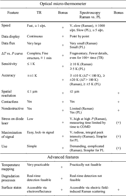
9.4.3 Dependence on heat spreader
Figure 9.5 shows ΔT versus I plots of 980 nm compressively-strained InGaAs/AlGaAs GRIN-SCH SQW ridge uncoated lasers 5 μm wide recorded under different conditions. First, the dependence on the use of a thick Au heat spreader (HS) layer on top of the p-contact (Figure 9.5b) is shown in (A) and (B) of Figure 9.5a. The graphs clearly show a decrease in the temperature for devices with the HS lined up with the mirror edge (B), in contrast to devices with the HS recessed (A) by ~20 μm (Figure 9.5b). The averaged drop in temperature is by a factor of two measured at the 60 mW mark of the three devices in each group. This difference can be understood from the fact that the temperature decreases exponentially from the mirror surface toward the laser cavity, which will be discussed in detail in Section 9.6 below.
Figure 9.5 Maximum temperature rise ΔT versus drive current I plots measured by TR on uncoated mirrors of 5 μm ridge InGaAs/AlGaAs SQW lasers depending on a heat spreader (HS) on top of the structure (b). (a): (A) HS ![]() 20 μm recessed; (B) HS lined up with mirror edge; (C) after COMD of device marked # in comparison to as-grown device in (B).
20 μm recessed; (B) HS lined up with mirror edge; (C) after COMD of device marked # in comparison to as-grown device in (B).
The second effect deals with the emergence of the kink at Ith in the ΔT/I characteristic after a COMD event occurred. The characteristics of as-grown lasers in (A) and (B) of the figure show no kink at threshold and thus are dominated by the Joule heating of the drive current. However, after COMD occurred a distinct kink at threshold appeared, as demonstrated by the characteristic marked # in (B) for the as-grown facet and (C) for the facet after COMD. This demonstrates in a distinct manner the superposition of laser radiation heating caused by surface absorption effects as argued already on many occasions in the text, in particular in Sections 7.4.6.1 and 8.2.3.1.
9.4.4 Dependence on mirror treatment and coating
A similar topic has been discussed in Section 7.4.6.2 on ridge (Al)GaAs lasers 7 μm wide in a ΔT versus P dependence representation by using Raman spectroscopy for measuring the mirror temperature rises ΔT. Here, we discuss ΔT versus I measurements on (Al)GaAs devices 10 μm wide with similar mirror treatments and coatings achieved, however, using the TR technique (Epperlein, 1993). The objective is to quantify the mirror surface quality/heating efficiency by the slope of signal rise at threshold relative to the current-heating signal slope below threshold.
Figure 9.6 shows the graphs for (i) uncoated, (ii) oxygen-ashed, λ/2–Al2O3-coated, (iii) oxygen-ashed, wet-etched, λ/2–Si3N4-coated, and (iv) λ/2–Al2O3-coated mirrors with the differential temperature increases δ(ΔT)/δP ![]() 1.0, 0.8, 0.2, and 0.1 K/mW, respectively.
1.0, 0.8, 0.2, and 0.1 K/mW, respectively.
Figure 9.6 TR facet temperature rises ΔT measured on (Al)GaAs SQW lasers 10 μm wide with different mirror treatments and coatings. Differential temperature increases per power unit at threshold are listed for the various mirror technologies to compare the respective mirror surface qualities/heating efficiencies.

What is remarkable is the reduction of heating due to optical power absorption by a factor of 4 due to the removal of the damage layer after an oxygen-ashing treatment by a wet etch. In addition, measurements on mirrors with the same surface treatment prior to coating showed no significant difference in ΔT between λ/2–Al2O3 and λ/2–Si3N4 passivation layers.
Finally, the signal of the slightly convex characteristics near the zero-point I ![]() 0 can be ascribed to electroreflectance caused by a surface potential modulated by the pulsed carrier injection during the TR measurement. This interpretation is in agreement with results from electric field-induced Raman scattering (EFIRS) measurements (Beeck et al., 1989) on the band bending of laser mirror surfaces.
0 can be ascribed to electroreflectance caused by a surface potential modulated by the pulsed carrier injection during the TR measurement. This interpretation is in agreement with results from electric field-induced Raman scattering (EFIRS) measurements (Beeck et al., 1989) on the band bending of laser mirror surfaces.
9.4.5 Bent-waveguide nonabsorbing mirror
A nonabsorbing mirror (NAM) structure based on a bent-waveguide concept has been discussed in Section 4.3.4 to enhance the optical strength of the laser facet. In this approach, the optical beam is decoupled from the active waveguide layer into the nonabsorbing cladding layer with a higher bandgap energy (Gfeller et al., 1992a, 1992b). As described previously, the bent-waveguide structure in the mirror regions of ridge (Al)GaAs lasers 3.5 μm wide is formed by overgrowing a wet-etched channel 1 μm deep with 22° sloped sidewalls in the n+-doped (100) GaAs substrate. Exact wafer orientation is necessary to obtain symmetrical growth conditions on both channel slopes.
To assess the effectiveness of the NAMs with respect to a reduction of optical absorption, the rise of mirror temperatures ΔT of lasers with dry-etched (CL2 reactive ion etching) and λ/2–Al2O3-coated mirrors has been measured for the first time for progressive NAM section lengths x in the range −1 < x < 16 μm by spatially resolved (![]() 1 μm) TR.
1 μm) TR.
Figure 9.7 shows the schematics of the NAM structure and, for illustration, the ΔT/I characteristics at three typical positions x = −1, 5, and 15 μm with high, low, and high temperatures measured for example at 30 mW for each device, respectively. This temperature behavior is also clearly reflected in the differential temperature increase at threshold, which is lowest for a device with a NAM section length x = 5 μm. The characteristics can be accounted for by the properties of the conventional mirror at x = −1 μm, a NAM with a beam fully in the nonabsorbing cladding at x = 5 μm, and a NAM with a partially recoupled beam into the absorbing waveguide at x = 15 μm, respectively.
Figure 9.7 Scheme of a bent-waveguide nonabsorbing mirror (NAM) structure of dry-etched, coated (Al)GaAs lasers. Schematic side view of the beam propagation in the structure. Selected temperature ΔT versus current I characteristics recorded on mirror facets at different NAM section lengths x = −1, 5, and 15 μm. Scale valid along cavity in x direction.

A more detailed ΔT/x dependence is plotted in Figure 9.8, which can be divided into three distinct regions.
Figure 9.8 Experimental mirror temperature increases ΔT at 30 mW quasi-cw power (top) and pulsed COMD power levels (bottom) for etched and passivation-coated mirrors of (Al)GaAs lasers 5 μm wide as a function of progressive nonabsorbing mirror (NAM) section length x. (Adapted in modified form from Gfeller et al., 1992a.) Dashed lines are guides to the eye.

In the region −1 < x < 2 μm (transition from conventional mirror to sloped waveguide section) the temperature measured at 30 mW optical output power falls sharply from typically 50 to 20 K.
In the range 2 < x < 10 μm (optical beam propagating fully in nonabsorbing cladding), the temperature remains at this low level of 20 K, and increases again for x >10 μm (partial beam recoupling into the absorbing waveguide leads to increased heating; recoupling is evidenced by monitoring the optical near-field patterns, see Figure 4.5).
The finite temperature of 20 K at the minimum may be due to nonradiative recombination of diffused carriers from the pumped laser section and to residual optical power absorption at surface defects of the etched mirrors as supported by the well-pronounced onset at threshold in the ΔT/I plots. Further improvements might be achieved by introducing a current blocking layer and by improved mirror etching and coating techniques.
The temperature profile in Figure 9.8 can be interpreted as a demonstration of nonradiative carrier recombination due to optical power absorption depending on the degree of overlap of the optical field intensity with the absorbing waveguide profile. The ΔT(x) profile is anti-correlated with the COMD(x) profile, as expected (see also Figure 8.4 for comparison). For lasers with observed partial beam recoupling (x > 10 μm), the COMD power shows a downward trend due to an increasing overlap of the optical beam with the absorbing waveguide. The effective length of the NAM section for this particular geometry is in the range 2 < x < 10 μm. Lasers with NAM lengths in this range show a fourfold improvement in the pulsed (500 ns at 0.1% duty cycle) COMD power levels compared to lasers with conventional mirrors (x < 0). A similar or even better improvement has also been achieved for cw-measured COMD power levels on lasers with x = 4 μm NAM section lengths.
9.5 Diode laser mirror studies by micro-thermoreflectance
9.5.1 Motivation
For many applications it would be useful to apply a nondestructive, contactless, sensitive, and fast microprobe to monitor local variations of material and laser device properties with high spatial resolution in the (sub)micrometer regime and in real time. These requirements can be fully met by the RM or TR techniques. Application examples include real-time temperature-monitored laser degradation effects, threshold and heating distribution within the near-field pattern, which will be discussed in this section, and laser facet temperature mapping investigations, which will be dealt with in the last section of this chapter.
9.5.2 Real-time temperature-monitored laser degradation
The discussion in this section deals with three effects first investigated by Epperlein (1990, 1992, 1993, 1997). They comprise the temperature leading to the COMD event, temperature during time to COMD, and temperature associated with dark-spot defect formation.
9.5.2.1 Critical temperature to catastrophic optical mirror damage
Typical examples of ΔT/Id characteristics of passivation-coated (Al)GaAs lasers with ridge waveguide widths of 5–10 μm are shown in Figure 9.9a, c, d. In all three cases depicted in the figure, the lasers incurred COMD at a critical temperature increase ΔTcr in the range of 110 to 120 K obtained in a quasi-cw operation (see Section 9.1.2). The existence of a critical temperature is consistent with the thermal runaway model for COMD discussed in Section 3.2.2.3. The heating of the mirror surface, together with the rapid exponential increase in the absorption coefficient with temperature, causes the surface to switch into a highly absorbing state for the laser radiation. Bandgap shrinkage and absorption increase form a positive feedback cycle at the critical temperature, ultimately leading to thermal runaway and catastrophic self-destruction of the mirror.
Figure 9.9 Mirror temperature rises ΔT as function of drive current Id for ridge (Al)GaAs lasers with different widths and passivation coatings (a), (c), (d) demonstrating the onset of COMD at a critical temperature increase ΔTcr. (a) P/I plot with partial COMD event shown for comparison. (b) ΔT/Id plot for device in (a) after (partial) COMD event with increased threshold current and reduced power and a quasi-periodic structure at large currents due to an optical power periodically increasing and decreasing with Id (not shown).

Figure 9.9a shows for illustration the critical temperature in the ΔT/Id graph in correlation with a drop in power P due to partial COMD shown in the P/Id characteristic. The critical temperature obtained for an (Al)GaAs laser in Figure 7.28 by Raman measurements can be considered to be in reasonable agreement with the data obtained here. This conclusion takes into account an overall measurement error of at least ±10 K and the fact that the samples were different in ridge geometry and mirror technology, which might have an effect on the critical temperature. Figure 9.9b shows the ΔT/Id after partial COMD (Figure 9.9a) with an increased threshold current and a quasi-periodic structure at higher drive currents Id with power values periodically increasing and decreasing with Id (not shown).
The quasi-cw critical temperature values are compatible with cw and quasi-cw measurements of COMD powers of broad-waveguide, 100 μm stripe InGaAs lasers (Botez, 1999). The critical temperature is practically independent of facet treatment and coating, but is dependent on the semiconductor material system used. The advantage of the TR technique is that the critical temperature can be determined at the very moment the COMD event is occurring by simply ramping up the current (power).
9.5.2.2 Development of facet temperature with operation time
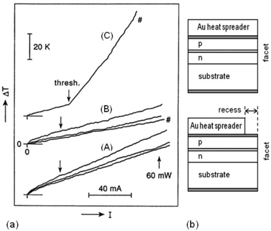
The time development of mirror temperature is demonstrated on a cleaved uncoated InGaP/AlGaInP–AlGaAs DQW 5 μm ridge laser operated at 30 mW.
Figure 9.10 shows a gradual increase of the temperature up to the time t where the mirror rapidly switches at ΔTcr ![]() 90 K into partial COMD (see sharp drop of optical power in P/t characteristic and residual power after COMD event). It reaches a maximum of ~320 K within ~1 s (detection system limited). The degraded output power then causes a rapid decay of the temperature, which finally settles at a steady state value. The actual temperature in the thermal runaway phase is much higher than the 320 K and can only be determined by using a sufficiently short time constant in the lock-in measurement of the TR signal. Furthermore, a maximum temperature response can only be expected when the probe laser spot truly hits the center of the hot spot at the facet. However, this cannot be predicted with sufficient precision, because the location where the hot spot will develop depends sensitively on the local heat and mechanical strain distributions under the ridge waveguide structure. Nevertheless, this experiment showed that COMD occurred in the (Al)GaInP laser system at a lower critical temperature increase of ~90 K compared to that in an (Al)GaAs laser material. It also demonstrated that, in principle, the dynamic behavior of thermal laser properties can be measured with the TR technique.
90 K into partial COMD (see sharp drop of optical power in P/t characteristic and residual power after COMD event). It reaches a maximum of ~320 K within ~1 s (detection system limited). The degraded output power then causes a rapid decay of the temperature, which finally settles at a steady state value. The actual temperature in the thermal runaway phase is much higher than the 320 K and can only be determined by using a sufficiently short time constant in the lock-in measurement of the TR signal. Furthermore, a maximum temperature response can only be expected when the probe laser spot truly hits the center of the hot spot at the facet. However, this cannot be predicted with sufficient precision, because the location where the hot spot will develop depends sensitively on the local heat and mechanical strain distributions under the ridge waveguide structure. Nevertheless, this experiment showed that COMD occurred in the (Al)GaInP laser system at a lower critical temperature increase of ~90 K compared to that in an (Al)GaAs laser material. It also demonstrated that, in principle, the dynamic behavior of thermal laser properties can be measured with the TR technique.
Figure 9.10 TR mirror temperature rise ΔT as function of time of an uncoated (Al)GaInP laser 5 μm wide operated at 30 mW. Demonstration of the onset of COMD at a critical temperature increase (~90 K) after a certain elapsed time. Indicates the formation of active defects with a concentration sufficient to initiate the COMD process. Power versus time plot is shown for comparison.
9.5.2.3 Temperature associated with dark-spot defects in mirror facets
The temperature associated with the gradual formation of a dark-spot defect (accumulation of localized nonradiative recombination defects, see Section 3.2.2.2) has been measured on a cleaved uncoated ridge (Al)GaAs laser facet 15 μm wide (Figure 9.11).
Figure 9.11 Temperature rise ΔT versus power P characteristics of an uncoated mirror of a ridge (Al)GaAs SQW laser 15 μm wide: (a) as-grown mirror without degradation; (b) facet degraded with dark-spot defect formation in center of near-field pattern (see inset).

Temperature and dark spot have been monitored or imaged simultaneously as a function of time. The figure shows the temperature increase ΔT as a function of the logarithm of optical power P for an as-grown laser and a degraded laser with dark-spot formation at the mirror facet. The temperature in the dark spot grew at a rate of ~5 K/h of operation at 25 mW quasi-cw optical output power. The growth rate depends on the effective local mirror temperature.
9.5.3 Local optical probe
This section demonstrates for the first time how the electro-optical and thermal properties within the near-field pattern of a diode laser can be probed by using the reflectance modulation technique.
9.5.3.1 Threshold and heating distribution within near-field spot
Figure 9.12 shows the ΔR/R versus Id characteristics around laser threshold at different random locations within the near-field pattern of a slightly degraded (Al)GaAs laser exhibiting two-mode behavior.
Figure 9.12 Local normalized reflectance change ΔR/R versus Id characteristics around laser threshold at different random locations within the near-field pattern of a slightly degraded (Al)GaAs laser exhibiting two-mode behavior. Characteristics displaced vertically for clarity. Linear approximations (thin lines) of the curves. Demonstration of local threshold and heating strength variations within filament structure of lateral mode profile.
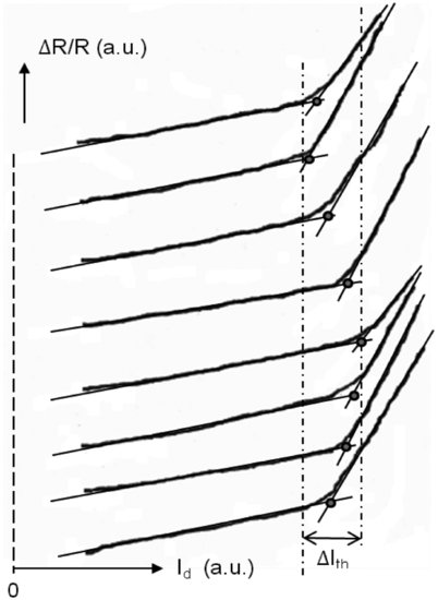
The characteristics are displaced vertically for clarity. Below the local thresholds, the characteristics have practically the same shape and slope, whereas the local threshold points and slopes of the characteristics beyond the thresholds vary strongly depending on the location within the near-field spot. In a first attempt, both effects can be made plausible within the concept of the filamentation phenomenon (discussed in various sections of Chapter 2), where the individual filaments within the lateral mode profile along the cavity have different thresholds and heating strengths. A partial correlation between local optical density within the near field and local threshold current could be found in the first measurements, but more detailed and systematic investigations are required to verify the effect.
9.6 Diode laser cavity temperatures by micro-electroluminescence
9.6.1 Motivation
The maximum laser optical output power is limited either by COMD or output power saturation due to heating of the active layer. High junction temperatures have important consequences for laser efficiency and threshold current, since both of these quantities are strongly temperature dependent (see Sections 1.3.7.1, 2.4.5.3, and 1.3.7.3). Therefore, it is crucial to measure the junction temperature under operating conditions. In addition, knowing the temperature profile along the cavity can give useful information about facet heating mechanisms, the effectiveness of a heat spreader, and mounting the laser chip onto a heat sink, and can reveal hot spots caused by heating through nonradiative recombination at high concentrations of defect centers.
Different methods have been used to measure the temperature inside the laser cavity including measuring the spectral shift of electroluminescence (EL) through a window in the epitaxial-side p-contact metallization (Brugger and Epperlein, 1990; Dyment et al., 1975) and GaAs substrate-side n-contact metallization (Dabkowski et al., 1994). Here, we discuss laser cavity temperatures obtained from spectral shifts of the active layer EL emitted on the side of a standard ridge laser chip cleaved close (<5 μm) to the ridge waveguide all along the cavity (Epperlein and Bona, 1993; Epperlein, 1997).
9.6.2 Experimental details – sample and setup
Figure 9.13a shows a sample prepared by cleaving a standard ridge (Al)GaAs laser chip in close proximity (<5 μm) to the ridge along the cavity of total length 750 μm with a maximum deviation of no more than 1 μm. The cleaved edge of total length 750 μm was magnified 350× and projected by appropriate optics perpendicular to the entrance slit of a 0.85 m spectrometer (Figure 9.13b). The magnified EL light line was moved perpendicular to the spectrometer slit with a typical width of ![]() 300 μm and thus a lateral resolution of
300 μm and thus a lateral resolution of ![]() 1 μm could be achieved.
1 μm could be achieved.
Figure 9.13 Laser cavity temperatures measured by spatially resolved electroluminescence (EL): (a) ridge waveguide laser sample preparation; (b) measurement principle; (c) and (d) partial EL light line images toward both cavity ends with two dark-spot areas in (d) due to local defect formation after thermal rollover of laser. Bright areas indicate high luminescence signal.
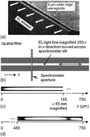
The laser was driven by current pulses at a low repetition rate of 200 Hz and d.c. of 50% and the EL emission after dispersion was detected by a suitable detector and phase-sensitive lock-in system. The radiation emitted laterally through the cleaved face originates in the active QW region and escapes from the sample without reabsorption in the higher energy layers of the laser structure. Figure 9.13c shows for illustration part of the uniform EL light line near one end of a laser cavity, whereas part of the EL light with two dark spots (hot spots) that occurred after thermal rollover operation of the laser can be seen close to the other end of the cavity (Figure 9.13d).
9.6.3 Temperature profiles along laser cavity
Typical EL spectra of the GRIN-SCH QW emission of a 5 μm ridge (Al)GaAs laser mounted onto a heat sink are plotted in Figure 9.14 for a cw laser output power of 13 mW. The spectra were recorded from close to the front mirror along the cavity in 1 μm steps and included the scattered laser light which was not blocked to be used as a reference. The spectral position of the EL QW peak shifts clearly to lower energies on approaching the mirror position, which indicates an increase in temperature due to the dominating temperature dependence of the bandgap energy.
Figure 9.14 EL spectra of a 5 μm ridge (Al)GaAs laser with dominant GRIN-SCH SQW emission recorded at 300 K and 13 mW cw in 1 μm steps from the front mirror along the cavity. Spectra are displaced vertically for clarity.

By using an experimentally determined temperature coefficient of the peak energy of dE/dT ![]() −0.54 meV/K (corresponding to dλ/dT
−0.54 meV/K (corresponding to dλ/dT ![]() 3 Å/K), which is in excellent agreement with the calculated temperature coefficient of the bandgap energy for GaAs derived from Figure 9.1, the temperature profile ΔT(x) along the cavity can be determined. Figure 9.15a shows the plot of log ΔT versus x for a ridge InGaAs/AlGaAs and GaInP/AlGaAnP-AlGaAs diode laser.
3 Å/K), which is in excellent agreement with the calculated temperature coefficient of the bandgap energy for GaAs derived from Figure 9.1, the temperature profile ΔT(x) along the cavity can be determined. Figure 9.15a shows the plot of log ΔT versus x for a ridge InGaAs/AlGaAs and GaInP/AlGaAnP-AlGaAs diode laser.
Figure 9.15 Cavity temperatures measured by spatially resolved EL for an InGaAs/AlGaAs and GaInP/AlGaInP–AlGaAs SQW laser. (a) Log of temperature rise ΔT versus coordinate x along cavity plots show for both lasers the same steep exponential decay of ΔT with a characteristic length of ~6 μm (1/e point) followed by a much slower but different decay toward the bulk of the cavity. (b) Temperature rises ΔT taken as a function of drive current Id near the center of the cavity are proportional to the square of Id in line with the expected Joule heating power of the drive current.
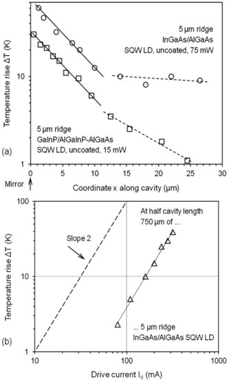
Both profiles exhibit in the first part an exponential decay of ΔT toward the cavity with a characteristic length of ~6 μm at the 1/e point. Beyond x > 10 μm the ΔT decays are also approximately exponential but slower and different for the two material systems. In this regime, the temperature slowly approaches a constant value effective for x > 25 μm. The overall ΔT(x) profile has a bathtub-like shape with high temperatures at the mirror sides and low temperatures in the center regions of the cavity. To achieve an efficient cooling effect by using a heat spreader on top of the structure, it has to be lined up with the mirror edge; a heat spreader recessed by the characteristic decay length or more has no measurable cooling effect on the mirror.
Finally, Figure 9.15b shows the dependence of ΔT on drive current Id in a log–log graph measured at a half-length position in the cavity. The cavity temperature is strongly proportional to the Joule heating of the drive current given by I2d, which is illustrated in the figure. The temperature rise in the cavity center of a 5 μm ridge uncoated InGaAs/AlGaAs laser is ΔT ~ 40 K at 300 mA (150 mW).
9.7 Diode laser facet temperature – two-dimensional mapping
9.7.1 Motivation
Knowledge of the two-dimensional temperature distribution on a laser facet can give useful information about local hot spots, the quality of facet passivation treatment and reflectivity coating layers, the bond between coatings and the semiconductor surface, and can contribute to the optimization of the vertical structure to achieve the goal of lowest possible absolute operating temperatures and temperature gradients.
The first ever mirror temperature map of an operating diode laser was obtained by the author (Epperlein, 1990) and reported in subsequent papers (Epperlein and Martin, 1992; Epperlein, 1993, 1997).
9.7.2 Experimental concept
Temperature maps have been obtained by raster scanning the focus spot of the low-power probe laser across the mirror surface of the quasi-cw square-pulse power-modulated diode laser (see Section 9.1.2). The high spatial resolution (~0.8 μm FWHM optical spot size) two-dimensional scanner with two orthogonally mounted high-precision (0.1 μm mechanical step size) stepping motor-driven translation stages, discussed in Section 7.1.2 and Figure 7.2, was employed in this application. The ΔR/R signal was detected as a function of location and, after conversion to temperature, a ΔT map was generated.
9.7.3 First temperature maps ever
A contour map of a typical temperature rise (relative to 300 K) distribution on an as-cleaved and uncoated mirror of a 15 μm wide ridge and 750 μm long InGaAs/AlGaAs GRIN-SCH SQW laser, quasi-cw square-pulse operated at a power P = 40 mW, is displayed in Figure 9.16.
Figure 9.16 Contour map of the temperature rise ΔT distribution recorded by scanning TR on a cleaved uncoated mirror facet of an (Al)GaAs diode laser 15 μm wide operated at 40 mW quasi-cw. The scan was not exactly parallel in the horizontal y direction, which caused a slight displacement in the z direction of the contour indents on both sides due to the epitaxial layer/substrate interface (see arrow) with different thermal conductivities in both regions. The effect of the latter is demonstrated by the different widths of the isothermal contour lines and the different slopes of the two sections in the ΔT versus z line scan. Note that the scale in the y direction is smaller than that in the z direction.

The scanned area is 35 μm×15 μm with the first scan aligned along the active layer approximately 0.5 μm (residual thickness, see Section 2.3) away from the lower edge of the etched ridge profile. Note that the scale in the y direction is smaller than that in the z direction.
There are two striking features: first, a very localized hot spot with a strong temperature rise ΔT ~ 60 K within the near-field pattern just below the ridge characterized by the dense 2 K equidistant contour lines; and, second, a much lower temperature regime characterized by the wider contour lines indicating a slower decay of temperature. This regime is in the GaAs substrate as indicated by the arrow marking the boundary line between the epitaxial (mainly) AlGaAs layers and the GaAs substrate. The ratio of the temperature decay strength in the GaAs and AlGaAs is fully consistent with the thermal conductivity that is about 5–6 times larger in GaAs than in AlGaAs. The two different temperature zones are also clearly demonstrated in the line scan shown in the figure. The contour map exhibits particularly well the epilayer/substrate interface with the indent of the isothermal lines becoming more pronounced in the horizontal y direction and the bending of the contour lines away from the heat source due to the strong heat-spreading effect of the top p-metallization.
9.7.4 Independent temperature line scans perpendicular to the active layer
A high-precision temperature line scan perpendicular to the near-field pattern of an E2-passivated (see Section 4.2.2.1), Al2O3-coated front mirror (R = 0.1) of a compressively-strained InGaAs/AlGaAs GRIN-SCH SQW single-mode high-power diode laser with a ridge 4 μm wide is shown in Figure 9.17. The temperature measurements were recorded at an output power of 110 mW for two separate runs and with a spatial resolution of 0.8 μm FWHM.
Figure 9.17 Temperature line scan ΔT versus z direction perpendicular across the near-field spot center of an InGaAs/AlGaAs SQW laser 4 μm wide at high power of 110 mW cw toward the GaAs substrate in two separate scans. The log ΔT versus z graph in the inset shows an exponential decay of ΔT in both epitaxial and substrate areas in agreement with the respective thermal conductivities in these areas.

The figure shows the hot spot area within the near-field pattern with a spot size of ~2 μm FWHM in the vertical direction, which is ~3× higher than the effective extension of the near field. The decay of the temperature toward the substrate side is divided into the two zones comprising the epitaxial layers and the substrate as demonstrated in an impressive manner by the log ΔT versus z coordinate graph of the inset confirming, for the first time, exponential decay in both areas. The slope ratio of the two experimental log curves is in excellent agreement with the ratio of the relevant thermal conductivities in the two regions confirming the result obtained in the section above.
9.7.5 Temperature modeling
The experimental ΔT map can be compared to heat flow calculations. From a theoretical point of view, the temperature distribution in the laser can be obtained by solving the three-dimensional heat equation in the device. For simplicity, however, we can neglect any variation of heat production that may occur along the laser structure. Therefore, we can limit the calculations to a cross-section of the laser where a solution of the two-dimensional heat equation must be found:
where k is the heat conduction coefficient, Q the heat source, h the convective heat transfer coefficient, and Text the external temperature. We further neglect particular thermal effects at the mirror including laser radiation absorption and nonradiative recombination effects and any convective heat transfer (h = 0) and external temperature (Text = 0) in the numerical computation process. The heat flow calculations make use only of the different thermal conductivities in the various sections of the structure and thus can give only a qualitative picture of the temperature distribution in the laser facet. We used the Partial Differential Equation (PDE) Toolbox within MATLAB (The MathWorks Inc., 1997) to solve the elliptic PDE in Equation (9.4), in order to determine the steady state temperature distribution.
9.7.5.1 Modeling procedure
We consider that heat is produced in the active layer, in a region that corresponds approximately to the near-field pattern of the diode laser. Neglecting radiation and convection losses at the surfaces of the device, we assume that heat can flow only through the substrate to a heat sink. The temperature at the bottom of the heat sink is held constant at 300 K. The PDE solving process can be divided into the following steps:
Figure 9.18 Mirror temperature map modeling using the MATLAB Partial Differential Equation Toolbox. (a) Simplified ridge structure – zoomed in. (b) Mesh pattern – zoomed in, used in finite element method to discretize the two-dimensional heat partial differential equation and produce approximation to solution.

The laser device parameters including dimensional, heat conduction, and heat source data used for the temperature modeling are listed in Table 9.2.
Table 9.2 Laser device parameters and data used in the mirror temperature map modeling. The various thermal conductivity values are from the Ioffe Physico-Technical Institute (2001), Carlson et al. (1965), Afromowitz (1973), and Adachi (1983).

9.7.5.2 Modeling results and discussion
Figure 9.19a shows the calculated mirror temperature map ΔT(y, z) of the laser used in Section 9.7.3 in excellent qualitative agreement with the experimental contour plot of Figure 9.16. In particular, the contrast and contour images show the hot spot area with its highest temperatures at the heat source of the active layer and with a steep temperature decay in the epitaxial region toward the substrate side due to a lower thermal conductivity in the epitaxial Al0.35Ga0.65As layers than in the GaAs substrate. The wider contour lines towards the p-contact indicate the strong heat spreading effect of the metallization.
Figure 9.19 Numerical computation of the temperature map ΔT(y, z) of the laser used in Figure 9.16 by considering only the different thermal conductivities of the various layers in the vertical laser structure. The modeling does not consider mirror heating effects due to laser radiation absorption and nonradiative recombination. (a) Contrast and contour image in good qualitative agreement with experimental temperature map of Figure 9.16. (b) First temperature gradient map of a diode laser mirror with strong gradients below the active layer as heat source toward the epitaxial layer/substrate interface, and along the silicon nitride layer.

The maximum temperature of ΔT ~ 10 K is in agreement with the cavity temperature measured toward the center of the cavity caused mainly by the distribution of the different thermal conductivities in the structure. The difference between maximum ΔT values of the calculated map (Figure 9.19a) and the experimental map (Figure 9.16) is due to laser radiation absorption and nonradiative recombination effects at the facet not taken into account in the numerical computation. The ratio of six between both values is in reasonable agreement with temperature measurements made from the mirror edge along the laser cavity (Figure 9.15).
Finally, Figure 9.19b exhibits for the first time a calculated temperature gradient map across the mirror facet. There are two striking areas where the gradients are highest. One is, as expected, below the active layer to the boundary with the substrate, whereas the other is in the dielectric Si3N4 layer along the lower edges of the ridge profile, but most importantly also along both ridge slope sides.
Considering the different thermal expansion coefficients of ~14×10−6 K−1, ~3×10⁻⁶ K−1 (Suganuma et al., 1985) and ~5.5×10⁻⁶ K−1 (Ioffe Physico-Technical Institute, 2001) for the dominating Au in the p-contact, Si3N4, and Al0.35Ga0.65As, respectively, these areas are potential sources for the formation of high thermal stress fields leading to high local stress amplitudes. The latter may trigger the formation of detrimental structural defects and cracks in the materials and may cause problems in the adhesion of the nitride and metallization layers.
These thermal stress fields superpose the intrinsic mechanical stress fields (see Section 8.2), caused by the deposition of the dielectric nitride and p-metallization layers at temperatures of ~120°C on ridge waveguide structures. As discussed in Section 8.2, local mechanical stress fields, which may now be enhanced through the superposition of both stress fields, are responsible for the formation and migration of defects (see Figures 8.8 and 8.9) resulting in an even stronger negative effect on diode laser performance and reliability.
References
Adachi, S. (1983). J. Appl. Phys., 54, 1844.
Afromowitz, M. A. (1973). J. Appl. Phys., 44, 1292.
Aspnes, D. E., Kelso, S. M., Logan, R. A., and Bhat, R. (1986). J. Appl. Phys., 60, 754.
Auston, D. H., McAfee, S., Shank, C. V., Ippen, E. P., and Teschke, O. (1978). Solid-State Electron., 21, 147.
Beeck, S., Egeler, T., Abstreiter, G., Brugger, H., Epperlein, P. W., Webb, D. J., Hanke, C., Hoyler, C., and Korte, L. (1989). Proceedings of ESSDERC'89, 508.
Botez, D. (1999). Appl. Phys. Lett., 74, 3102.
Brugger, H. and Epperlein, P. W. (1990). Appl. Phys. Lett., 56, 1049.
Cardona, M. (1969). Modulation spectroscopy. In Solid State Physics (eds. Seitz, F. et al.), Suppl. 11, Academic Press, New York.
Carlson, R. O., Slack, G. A., and Silverman, S. J. (1965). J. Appl. Phys., 36, 505.
Dabkowski, F. P., Chin, A. K., Gavrilovic, P., Alie, S., and Beyea, D. M. (1994). Appl. Phys. Lett., 64, 13.
De Freitas, L., da Silva, E., Mansanares, A., Pimentel, M., Filho, S., and Batista, J. (2005). J. Appl. Phys., 97, 104510.
Dyment, J. C., Cheng, Y. C., and SpringThorpe, A. J. (1975). J. Appl. Phys., 46, 1739.
Epperlein, P. W. (1990). Inst. Phys. Conf. Ser., 112, 633.
Epperlein, P. W. (1993). Jpn. J. Appl. Phys., 32, Part 1, No. 12A, 5514.
Epperlein, P. W. (1997). Proc. SPIE, 3001, 13.
Epperlein, P. W. and Bona, G. L. (1993). Appl. Phys. Lett., 62, 3074.
Epperlein, P. W. and Martin, O. J. (1992). Inst. Phys. Conf. Ser., 120, 353.
Gfeller, F. R., Buchmann, P., Epperlein, P. W., Meier, H. P., and Reithmaier, J. P. (1992a). J. Appl. Phys., 72, 2131.
Gfeller, F. R., Buchmann, P., Epperlein, P. W., Meier, H. P., and Reithmaier, J. P. (1992b). Proceedings of the IEEE 13th International Semicondoctor Laser Conference, Conf. Dig., 222.
Ioffe Physico-Technical Institute (2001). New Semiconductor Materials: Physical Properties. www.ioffe.rssi.ru/SVA/NSM.
Ju, Y., Käding, O., Leung, Y., Wong, S., and Goodson, K. (1997). IEEE Electron Device Lett., 18, 169.
Mansanares, A. M., Roger, J. P., Fournier, D., and Boccara, A. C. (1994). Appl. Phys. Lett., 64, 4.
Matatagui, E., Thompson, A., and Cardona, M. (1968). Phys. Rev., 176, 950.
Navitar, Inc. (2011). Products. http://navitar.com.
Piwoński, T., Wawer, D., Szymański, M., Ochalski, T., and Bugajski, M. (2005). Optica Applicata, XXXV, 611.
Piwoński, T., Pierscinska, D., Pierscinski, K., Malag, A., Jasik, A., Kozlowska, A., and Bugajski, M. (2006). Proc. Mater. Res. Soc. Symp., 916, DD06-01.
Schaub, E. (2001). Analytical Sciences (The Japan Society for Analytical Chemistry), 17 (Special issue), s443.
Seraphin, B. O. (1972). Chapter 1 in Semiconductor and Semimetals (eds. Willardson, R. K. and Beer, A. C.), 9, 1, Academic Press, New York.
Stern, F. (1964). Phys. Rev., 133, A1653.
Suganuma, K., Okamoto, T., Koizumi, M., and Shimada, M. (1985). J. Mater. Sci. Lett., 4, 648.
Sweeney, S., Lyons, L., Adams, A., and Lock, D. (2003). IEEE J. Sel. Top. Quantum Electron., 9, 1325.
The MathWorks, Inc. (1997). Products: MATLAB. www.mathworks.com.
Todoroki, S. (1986). J. Appl. Phys., 60, 61.
Varshni, Y. P. (1967). Physica, 34, 149.
Wawer, D., Ochalski, T. J., Piwoński, T., Wójcik-Jedlińska, A., Bugajski, M., and Page, H. (2005). phys. stat. sol. (a), 202, 1227.
Xi, Y., Xi, J., Gessmann, Th., Shah, J., Kim, J., Schubert, E., Fischer, A., Crawford, M., Bogart, K., and Allerman, A. (2005). Appl. Phys. Lett., 86, 031907.