
Chapter 7
Novel diagnostic laser data for active layer material integrity; impurity trapping effects; and mirror temperatures
7.1 Optical integrity of laser wafer substrates
7.1.3 Discussion of wafer photoluminescence (PL) maps
7.2 Integrity of laser active layers
7.2.3 Discussion of quantum well PL spectra
7.3 Deep-level defects at interfaces of active regions
7.3.3 Discussion of deep-level transient spectroscopy results
7.4 Micro-Raman spectroscopy for diode laser diagnostics
7.4.2 Basics of Raman inelastic light scattering
7.4.4 Raman on standard diode laser facets
7.4.5 Raman for facet temperature measurements
7.4.6 Various dependencies of diode laser mirror temperatures
Introduction
This chapter discusses optical uniformity of doped laser wafer substrates, impurity trapping effects in active laser quantum wells (QWs), deep-trap accumulation at active layer interfaces, and local laser mirror temperatures as a function of output power, laser material, vertical structure, number of active quantum wells, mirror coating, heat spreader, and the laser die mounting technique. Fundamentals and experimental setups of the relevant measurement techniques will also be discussed and include photoluminescence (PL) mapping, low-temperature PL spectroscopy, deep-level transient spectroscopy (DLTS) and Raman microprobe inelastic light scattering spectroscopy, respectively.
7.1 Optical integrity of laser wafer substrates
7.1.1 Motivation
Improving the performance and reliability of optical devices such as diode lasers requires that the electrical and optical material parameters be precisely controlled. This is true not only for the epitaxial growth of the individual layers of the laser structure, but also for the underlying wafer substrate these layers are grown on. Wafers used for diode lasers are typically n-type doped to yield an electron concentration of ~1.5×1018 cm−3, and standard wafers have a dislocation etch pit density of ~2×103 cm−2.
Any nonuniform distribution of dopants and defects can impact the performance and reliability characteristics of the laser and consequently the yield. The increasingly demanding requirements for materials with a high degree of purity and structural homogeneity place concomitantly higher demands on semiconductor growth, processing technologies, and the characterization techniques, which support these technologies. As mentioned above, in particular, knowledge of the spatial variation of the material parameters is vital because of possible correlations with device properties.
Optical techniques are particularly suited for two-dimensional imaging because they are fast, nondestructive, and noncontact. PL is a simple, but particularly sensitive and informative technique for detecting concentrations of imperfections as low as 1011 cm−3 in semiconductors. PL intensity maps, for example, of as-grown and processed GaAs or InP wafers contain information on material uniformity, dislocation density, density of deep traps, distribution of residual impurities, uniformity of epitaxial buffer layers, implant and anneal uniformity, and the presence of process-induced defects (Epperlein, 1990; Guidotti et al., 1987; Hovel and Guidotti, 1985).
In the following, we describe two PL scanning techniques, one for fast scanning of full 2 or 3 inch wafers at room temperature and the other for scanning at specific wafer locations with high spatial resolution of ~2 μm at 300 K and for spectrally resolved scans with a spatial accuracy of ~30 μm at 2 K. As an example, the PL mapping results of an n-type silicon-doped GaAs wafer will be discussed.
7.1.2 Experimental details
Figure 7.1 shows the setup of a simple “galvo” mirror scanner capable of producing within minutes digital maps of the dominating near band edge (NBE) PL at room temperature of full 2 (3) inch wafers with a resolution of ~50–100 μm. The wafer placed on a dc motor-driven stage is moved in one direction, while a focused laser beam is scanned in the orthogonal direction. The integrated PL light is detected by a long (typically 4 inch) Si p–n junction photodiode placed close to the wafer surface and parallel to the scanning direction of the focused laser beam. An edge filter in front of the photodiode blocks the laser light and transmits the PL signal for detection in the range ~1.1–1.6 eV. A personal computer correlates the lock-in amplified signal with the position on the wafer and displays the digitized signal on a monitor in high-resolution color or 8-bit grayscale contrast images. The minimum scanning field with this setup is ~9×9 mm2 corresponding to a ~30 μm resolution.
Figure 7.1 Schematics of the photoluminescence (PL) mapping system using a galvo mirror scanner.

The second optical mapping system is more sophisticated, capable of much higher spatial resolution and of producing spectrally resolved PL scans. Figure 7.2 shows the setup of the system, which has an operating principle similar to the one described in the literature (Luciano and Kingston, 1978; Yokokawa et al., 1984).
Figure 7.2 Schematic illustration of the high spatial resolution PL scanner for room temperature and cryogenic temperature integral intensity or spectrally resolved mapping applications.

The system consists essentially of two mirrors attached to two orthogonally mounted, high-precision (0.1 μm step size) stepping motor-driven translation stages. The horizontal X-stage moves the vertical Y-stage. Laser light is guided via a dichroic filter or polarizing beamsplitter along the axis of the horizontal stage onto the first mirror, directed vertically upward where the second mirror deflects the beam 90° perpendicular to the laser plane through the focusing lens onto the sample, which can be at room temperature or at low temperature in a helium bath cryostat. The lens fixed to the vertical stage is used both to focus the beam and to collect the PL emission. The way the mirrors and lens are mounted on the two stages insures that the beam always hits the same spot on the upper mirror and passes through the center of the lens during translation. The PL light follows the same optical path as the laser beam. After decoupling from the incident light by the dichroic filter or polarizing beamsplitter, the PL light is directed to a suitable detector or into a spectrometer for spectral analysis. The PL data are processed for evaluation and display in a computer system similar to that described above. By using a lens with a large numerical aperture (0.5), such as a 20× microscope objective, PL maps with high spatial resolution of ~2 μm and high collection efficiency can be recorded at 300 K. The spatial resolution of low-temperature (2 K) spectral maps is typically 30 μm.
7.1.3 Discussion of wafer photoluminescence (PL) maps
Figure 7.3a shows the grayscale contrast image of the 300 K NBE PL intensity of a full 2 inch Si-doped (100) GaAs wafer where the bright areas correspond to high PL signal. The GaAs is doped to a concentration of the shallow Si donors to yield an electron concentration in the range of 1.2 to 1.7×1018 cm−3 and has a standard etch pit density (EPD) of 2×103 cm−2. The 300 K PL spectrum is depicted in Figure 7.3b and consists of a broad asymmetric peak at 1.42 eV with a FWHM of 34 meV primarily due to thermal broadening. The peak can be ascribed to a free-to-bound recombination, in this case from an electron in the neutral Si donor level to a hole in the valence band (Do,h), while a small shoulder ~6 meV off the main peak in the upper part of the signal and on the high-energy side can be attributed to a band–band transition considering the fact that the binding energy of Si in GaAs is shallow at ~6 meV. In the next section we will discuss the major radiative recombination processes in a semiconductor.
Figure 7.3 Photoluminescence (PL) of a 2-inch, Si-doped n-type (100) GaAs wafer. (a) Grayscale contrast image of the near-band edge, integrated PL intensity distribution at room temperature. Bright areas: high intensity; dark areas: low intensity. (b) Room temperature PL spectrum. (c) Line scan of the integrated PL intensity across the wafer at the arrowed positions in (a).

The PL intensity map has an overall bowl-like pattern with high PL intensity at the wafer edges dropping toward the wafer center, which can also be clearly verified by the line scan in Figure 7.3c. The uneven and cloud-like PL distributions may be caused by Si striations and streaks during the GaAs ingot crystal growth.
These PL maps are totally different to the PL maps of semi-insulating (s.i.) (100) GaAs wafers grown by the so-called liquid-encapsulated Czochralski (LEC) method. The macroscale pattern of these maps shows the typical fourfold azimuthal symmetry superimposed on a radial W-type variation (Epperlein, 1990; Guidotti et al., 1987) predicted by a thermoelastic analysis of dislocation generation in s.i. (100) LEC-grown GaAs crystals (Jordan et al., 1980). The small-scale structure in these maps forms the well-known cellular network with cell sizes of a few hundred micrometers and can be fully correlated with the dislocation EPD (Epperlein, 1990). This effect can be explained in terms of intrinsic gettering of optically and electrically active defects to the dislocation cores during ingot formation and cooling, such that the dislocation network becomes visible. It is generally understood that the causes of NBE PL enhancement near dislocations are manifold, including lifetime variations of free carriers (Leo et al., 1987), spatial variations of deep-levels and shallow acceptor concentrations leading to spatially varying compensation (Wakefield et al., 1984), or a decrease of nonradiative centers forming a denuded zone (Cottrell effect) near dislocations (Chin et al., 1984).
In contrast, however, the local PL fluctuations observed in Figure 7.3a and in particular in the line scan of Figure 7.3c are by far less pronounced, and also show no regular pattern compared to those in maps and scans of s.i. GaAs wafers (Epperlein, 1990). We conclude therefore that the two-dimensional NBE PL distribution is caused primarily by a nonuniform distribution of Si dopants during ingot growth and not by dislocations. The PL intensity and hence the donor concentration can vary by up to a factor of two across the wafer with the consequence that the required electron concentration would be out of spec and too low for most of the wafer area. Laser devices grown on such wafer substrates would show deteriorated performance and reliability figures due to the increased series resistance and linked heating effects. The yield of in-spec devices would be drastically reduced.
7.2 Integrity of laser active layers
7.2.1 Motivation
It is known that the uncontrolled incorporation of impurities such as shallow acceptors in the nominally undoped active layer of molecular beam epitaxy (MBE) grown double-heterostructure (DH) and quantum well (QW) diode lasers and electrical devices such as heterojunction field-effect transistors (FETs) has a degrading effect on the performance and reliability of these devices. In particular, the impurity buildup at the inverted heterointerface (GaAs on AlGaAs) as compared to the normal AlGaAs on GaAs interface of AlGaAs/GaAs devices and the linked formation of point defects, traps, and interface roughness have been identified as potential root causes (Masselink et al., 1984a; Epperlein and Meier, 1990).
Intrinsic and impurity-related PL from nonintentionally doped AlGaAs/GaAs SQW and MQW structures has been studied systematically as a function of well width Lz, bottom AlGaAs cladding layer thickness, and various prelayer sequences (Epperlein and Meier, 1990). Detailed investigations of the dependence of the impurity binding energy on Lz identified carbon acceptors as the dominating impurity species. Carbon acceptors are trapped during growth at the inverted interface of the first in-a-sequence-grown QW. These inhibit the growth, for example, by preventing the lateral propagation of the atomic layers due to pinning steps on the surface and consequently leading to increased roughening of the interface and interface recombination velocity. This detrimental effect increases with increasing bottom cladding thickness but it can be drastically suppressed by growing so-called prelayers before the actual active QW layer.
In the next sections we describe, first, both the fundamental radiative transitions allowed in a semiconductor and the experimental PL setup capable of detecting efficiently and reliably the impurity-related PL emissions. For comparison, we also discuss detection of the intrinsic PL, in particular the faint and narrow lines of free and bound exciton recombinations only detectable at very low temperatures, such as 2 K, for example. We then discuss the various impurity-related effects and a procedure for effectively suppressing the gettering of background impurity atoms at the active layer during MBE growth, and thereby improve the performance of the laser device.
7.2.2 Experimental details
7.2.2.1 Radiative transitions
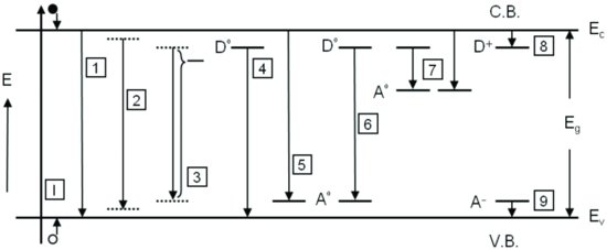
Figure 7.4 shows schematically the basic radiative recombination processes in a semiconductor following, first, a generation (I) of excess, nonequilibrium electron–hole carriers, for example, by an external light source with an above-bandgap energy Eg, and then a fast relaxation or thermalization process of the excited carriers to the band edges. The transitions can be classified and described as follows:
- (1): Band-to-band recombination, usually difficult to observe in weakly doped samples. More likely in less pure or less perfect crystals and at thermal energies kBT > Ex, the exciton binding energy leaving free carriers available to recombine radiatively in a band-to-band transition.
- (2): Free exciton (FE) recombination in a sufficiently pure material where electrons and holes pair off into excitons, which then recombine emitting a narrow spectral line. Energy of emitted photon in a direct gap semiconductor with momentum conservation in a simple radiative transition is hν = Eg − (1/n2)Ex1 with n the quantum number of the exciton excited states where Ex1
 4.4 meV (GaAs) is the exciton ground state (n = 1) energy. Probability of n > 1 exciton transitions decreases with n−3 (Elliott, 1957), difficult to observe in the presence of other radiative processes, electric fields (dopants), and temperatures >4 K (exciton breaking up into free carriers). Involvement of a phonon in an FE transition in an indirect gap material to conserve momentum; emitted photon energy reduced by the phonon energy. Narrow FE linewidths 1 meV for GaAs at 1 K.
 - (3): Bound exciton (BE) recombination in the presence of impurities. Emission with a narrow spectral width of typically 0.1 meV and at a lower photon energy than that of FE, for example, hν(Do,X) = Eg − E(Do,X) = Eg − Ex − 0.13ED (GaAs) with donor binding energy in GaAs ED 6 meV. Bound exciton transitions may be from neutral and ionized donors and acceptors in the forms (D°,X), (D+,X), (A°,X), (A+,X) where X designates the exciton bound to an impurity state. Process (3) in Figure 7.4 shows a donor bound exciton transition.
- (4) and (5): Band-to-impurity (free-to-bound (FB)) recombinations involving shallow impurities (hydrogen-like centers) characterized by (h,D°) and (e,A°) where a neutral donor state interacts radiatively with a hole in the valence band and an electron from the conduction band transfers to a neutral acceptor state, respectively. The photon energy is hν = Eg − Ei − Ep (in case phonons with energy Ep are involved in transition; phonon replicas) where Ei is 34 meV and 5.2 meV for the ionization energy for acceptors and donors in GaAs, respectively, calculated within a hydrogen model approximation. Occurs in samples with relatively low dopant concentrations, but is dominated in purer material by exciton recombination processes. From the spectra one can deduce the acceptor binding energies but less reliably donor binding energies due to the very small chemical shift of the donor atoms involved.
- (6): Donor–acceptor pair recombinations involve both donor and acceptor impurities and are characterized by (Do,Ao). The energy separating the paired donor and acceptor states is hν = Eg − (EA+ED)+q2/ɛr where the last term is the Coulomb interaction energy, which is very small for distant pairs (r large). The pair recombination is assisted by a tunneling process for donor and acceptor atoms separated by distances r greater than the effective Bohr radius. Distant pair recombinations are less likely than short-distance pair transitions leading to an increase of the emission intensity as r decreases, which in turn decreases the number of pairs. This means that the intensity must go through a maximum as r is changed in a discrete fashion resulting in an emission spectrum with discrete lines. The fine structure can be resolved for pair separations typically in the range of 1 to 4 nm for GaP; however, above this value the lines overlap and form a broad spectrum. In GaAs where EA+ED is small, only the large r-pairs contribute to the emission spectrum, because the Coulomb energy for small r-pairs drives the donor and acceptor levels into the conduction and valence bands, respectively. There, a pair recombination would have to compete with the band-to-band transitions, which involve high density of states, and hence a pair recombination would have to be very efficient to generate a line spectrum (Pankove, 1975). Typical of pair recombinations is the high-energy shift and narrowing of the spectrum with increasing excitation intensity, which can be ascribed to the saturation of long-distance pairs and dominance of short-distance donor–acceptor pairs.
- (7): Deep transitions involving the transition of an electron from the conduction band or from a donor to a deep-level with a large ionization energy Ei > 0.2 eV (GaAs). Formation of such deep-levels, for example, by complex centers, vacancy–impurity complex defects such as Ga vacancy–donor complex band structures near 1.2 eV in n-type GaAs, or by 3-d transition metals in III–V compounds. The figure shows the transitions to a deep acceptor level with its energy deep in the bandgap. These transitions yield very low photon energies.
- (8) and (9): Shallow transitions to ionized donors or acceptors. These transitions could be radiative in the far infrared. Although radiative transitions from the conduction band to the donor have been reported in GaAs (Melngailis et al., 1969), we consider a further discussion of this topic beyond the scope of this section.
Figure 7.4 Schematic diagram of the fundamental radiative recombination processes in a semiconductor. C.B. is the conduction band, V.B. the valence band.
7.2.2.2 The samples
Different AlxGa1−xAs/GaAs QW structures were grown by conventional MBE on (100) s.i. GaAs substrates. All structures were deposited on a superlattice (SL) buffer layer 0.6 μm thick followed by a bottom AlxGa1−xAs cladding layer of varying thickness LB ![]() 0.05–0.5 μm, the prelayer sequence consisting either of an SL or a GaAs SQW with thickness Lz1
0.05–0.5 μm, the prelayer sequence consisting either of an SL or a GaAs SQW with thickness Lz1 ![]() 0.8–12 nm. Further layers include an AlxGa1−xAs barrier layer with thickness Lb
0.8–12 nm. Further layers include an AlxGa1−xAs barrier layer with thickness Lb ![]() 0.03–0.5 μm, the test QW with Lz2
0.03–0.5 μm, the test QW with Lz2 ![]() 4–15 nm, and finally the upper AlxGa1−xAs cladding
4–15 nm, and finally the upper AlxGa1−xAs cladding ![]() 0.1 μm thick. The top test QW probes the efficiency of the prelayers as impurity trapping centers. In addition, several MQW samples were grown with different single-well widths in the range of 0.8 to 12 nm and sequences of the wells and with constant Lb = 30 nm. All layers are unintentionally doped with a p-type doping in the GaAs of about 2×1014 cm−3. The nominal AlAs mole fraction x of all AlGaAs layers was 0.3.
0.1 μm thick. The top test QW probes the efficiency of the prelayers as impurity trapping centers. In addition, several MQW samples were grown with different single-well widths in the range of 0.8 to 12 nm and sequences of the wells and with constant Lb = 30 nm. All layers are unintentionally doped with a p-type doping in the GaAs of about 2×1014 cm−3. The nominal AlAs mole fraction x of all AlGaAs layers was 0.3.
7.2.2.3 Low-temperature PL spectroscopy setup
The PL spectra were recorded at T = 2 K and higher temperatures at various laser excitation power densities in the range ~10−2–102 W/cm2. The samples were mounted stress-free in a variable temperature cryostat immersed in superfluid liquid helium or in a cold helium gas flow. After standard excitation by the 514.5 nm line of a cw argon-ion laser and appropriate dispersion in a 0.85 m, f/7.8 dual-holographic grating monochromator, the PL light was detected by a thermoelectrically cooled, selected GaAs photomultiplier tube (PMT) with low dark count rate and conventional single-photon pulse counting electronics or an optical multichannel analyzer (OMA) with a cooled charge-coupled device (CCD) detector array.
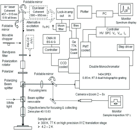
The state-of-the-art optical spectroscopy setup schematically illustrated in Figure 7.5 was a multipurpose system used by the author for many applications on different semiconductor materials and devices requiring high spatial resolution of ~1 μm and different temperatures in the range of 2 to 300 K and included PL spectroscopy, PL excitation (PLE) spectroscopy, Raman spectroscopy, electroluminescence (EL), thermoreflectance, and other suitable techniques (see Chapters 7–9). The cw dye laser was used as a wavelength-tunable excitation source for PLE spectroscopy measurements to determine the energies of the various free exciton transitions in the QW. The mechanical chopper was used for all applications not requiring signal detection by the PMT or CCD but only by a photodiode. The various polarization-dependent components in the laser excitation path were used in Raman spectroscopy measurements, see next sections below.
Figure 7.5 Schematics of a multipurpose, state-of-the-art optical characterization system for applications requiring techniques such as low-temperature PL spectroscopy, PL excitation (PLE) spectroscopy, Raman spectroscopy, electroluminescence (EL), and thermoreflectance (TR) with capabilities including high spatial and spectral resolution, high signal detection sensitivity, and variable temperatures in the range of 2 to 300 K. The Ar+ laser is used for PL, Raman and TR, the Ar+ laser-pumped dye laser for PLE, the He–Cd UV laser for III–nitride semiconductor PL, the mechanical chopper for light detection using a photodiode, and the various polarization components are used for Raman spectroscopy.
7.2.3 Discussion of quantum well PL spectra
7.2.3.1 Exciton and impurity-related recombinations
A typical 2 K PL spectrum of a MQW sample with SQWs 4, 15, and 8 nm wide is shown in Figure 7.6a where the 4 nm QW is the first in-a-sequence-grown well after the bottom AlGaAs cladding layer 500 nm thick. The spectrum of this 4 nm well shows a sharper peak on the high-energy side end and two broader peaks on the low-energy side (only visible with signal expansion by 20×), whereas the spectra of the subsequently grown 15 and 8 nm wells with 30 nm barriers each exhibit a dominating, high-intensity sharp emission, without signal expansion.
Figure 7.6 Photoluminescence (PL) spectra of AlGaAs/GaAs multi-quantum well (MQW) structures at low temperatures of 2 K. For clarity only the simplified conduction band portion of the MQW structures is shown. (a) MQW with 4, 15, 8 nm wide in-a-sequence MBE-grown QWs. (b) MQW with 8, 6 nm wide in-a-sequence grown QWs. Focus is on the shape of the PL spectrum of the 8 nm QW in (a) and (b).

The peak on the high-energy side of the 4 nm QW spectrum and the strong narrow lines in the 8 and 15 nm well spectra can be attributed to the intrinsic n = 1 free heavy-hole exciton recombination, FE(e1–hh1), with a photon energy E1h. We can exclude impurity (acceptor) bound exciton luminescence, which occurs only occasionally with an almost unobservable emission, Stokes-shifted from E1h by about 4 meV.
The lower intensity, sharp peaks on the high-energy sides (signal expanded 20×) of the dominating peaks in the 15 and 8 nm well spectra can be assigned to the n = 1 free light-hole exciton recombination, FE(e1–lh1), with a photon energy E1l. These E1h and E1l assignments have been concluded from the dependence of the PL intensity on excitation power and lattice temperature. The intrinsic PL intensity is nearly linear in excitation power, as expected for a monomolecular (excitonic) recombination process, and decreases by about 20% when the sample temperature is increased from 2 to ~30 K. For details see Epperlein and Meier (1990). PLE spectroscopy measurements and subband calculations confirm these assignments.
Figure 7.6b shows the spectrum of a MQW where an 8 nm SQW is grown first with a subsequent 6 nm well growth. In contrast, the 8 nm well now shows the reduced signal emission with two broader peaks on the low-energy side and the 6 nm well the dominating, high-intensity sharp emission with a narrow peak again on the high-energy side after signal expansion 10×. The various narrow emissions on the high-energy sides of the sub-spectra can again be ascribed to free exciton recombinations.
On the other hand, the extrinsic PL, that is, the intensity of the luminescence on the low-energy side of the intrinsic peak of the 4 nm well in Figure 7.6a and the 8 nm well in Figure 7.6b, tends to saturate at higher excitation powers (Epperlein and Meier, 1990). The presence of a limited number of impurities can plausibly account for such a saturation. This effect and the energy of the transition strongly suggest that it can be ascribed to the recombination of free electrons in the n = 1 quantum confined state with neutral acceptors in the QW, marked as (e1,A°). Donor–acceptor pair recombination can be ruled out for three reasons: (i) the intensity of the extrinsic peak is not very sensitive to temperature in the range of 2 to 20 K; (ii) the energy of the peak responds only slightly to the excitation intensity; and (iii) to temperature. Further evidence of the involvement of acceptors in the formation of the broad extrinsic PL emissions and their identification will be discussed in the next section.
Moreover, the presence of extrinsic QW PL correlates with the linewidth of the intrinsic exciton PL emission and with the thickness of the bottom cladding and barrier layers.
Figure 7.7a shows the intrinsic FWHM of the dominating intrinsic heavy-hole exciton recombination of different, nominally 8 nm wide wells plotted as a function of the extrinsic PL intensity normalized to the intrinsic intensity. These QWs have exciton wavefunctions, which only weakly penetrate into the barrier layers and therefore are sensitive to interfacial disorder. The figure shows that samples with practically no extrinsic PL have small linewidths of typically 2.5 meV indicating smooth and abrupt interfaces. The linewidth increases with increasing extrinsic PL signal and tends to saturate.
Figure 7.7 (a) Linewidth of the 2 K PL emission of the 8 nm well plotted as a function of the extrinsic acceptor-related PL intensity normalized to the intrinsic exciton-related PL intensity of the 8 nm well at low excitations of 1 W/cm2. (b) Simple interface roughness model estimating an average QW thickness fluctuation and ratio between island-covered area and island-free area. Solid line: calculated trendline.

Figure 7.7b describes a simple model for the average interface roughness ![]() based on the Lz dependence of the quantum confined energy (cf. Equation 1.19) and by using the maximum observed FWHM of 8 meV. The model calculates
based on the Lz dependence of the quantum confined energy (cf. Equation 1.19) and by using the maximum observed FWHM of 8 meV. The model calculates ![]()
![]() 0.02 nm and evaluates the lateral extension of the roughness expressed by the ratio between the island-covered area Awith and the island-free area Aw/o to roughly 10%. It is well known that monolayer fluctuation steps of the well thickness can be the source of formation of deep-levels and nonradiative recombination centers, which can strongly impact the efficiency and threshold of the diode laser and its long-term lifetime. Line broadening due to band filling via charge transfer from the acceptor impurities at the interfaces was estimated to play only a minor role.
0.02 nm and evaluates the lateral extension of the roughness expressed by the ratio between the island-covered area Awith and the island-free area Aw/o to roughly 10%. It is well known that monolayer fluctuation steps of the well thickness can be the source of formation of deep-levels and nonradiative recombination centers, which can strongly impact the efficiency and threshold of the diode laser and its long-term lifetime. Line broadening due to band filling via charge transfer from the acceptor impurities at the interfaces was estimated to play only a minor role.
7.2.3.2 Dependence on thickness of well and barrier layer
More information on the acceptors involved in the (e1,A°) transition, in particular on their energetic states and identification, has been obtained by determining the acceptor binding energy E(A°) as a function of Lz, which varied in the range ~1–12 nm in many samples grown at the residual MBE background pressure.
E(A°) was evaluated in the usual way (Miller et al., 1982) from E(A°) = E1h − E(e1,A°)+B(1h) = Eg − E(e1,A°), where E1h is the n = 1 free heavy-hole (hh) exciton transition energy, E(e1,A°) the energy of the broad peak(s) of the extrinsic PL, B(1h) the binding energy of the n = 1 ground state hh exciton, and Eg the n = 1 QW energy gap. E(A°) is the energy necessary to transfer a hole from A° to the n = 1 hh level in the valence band of the well. The actual Lz values of the various QWs were determined from calculations of the transition energies and by using the experimental E1h values.
The experimental data plotted as E(A°) versus Lz fall distinctly into a low-energy and high-energy branch and increase with decreasing Lz. The interested reader is referred for further details to the original publication of Epperlein and Meier (1990). This splitting into two components can be expected, since the acceptor density of states is strongly enhanced at the well center and interface positions (Masselink et al., 1984b; Bastard, 1981). The lowering of the binding energy for on-edge impurities compared to on-center impurities is a direct consequence of the repulsive interface potential, which tends to push the hole charge distribution away from the attractive ionized acceptor center leading to a reduced effective Coulomb attraction.
It was demonstrated for the first time that the experimental data in the upper and lower branch are in good agreement with calculations (Masselink et al., 1984b) for the ground state of neutral carbon acceptors (C°) at the center and at the interfaces of Al0.3Ga0.7As/GaAs QWs, with typical binding energies E(C°) of 37 and 23 meV for a 6 nm QW, respectively (Epperlein and Meier, 1990). In addition, control experiments on samples grown in a beryllium background atmosphere leading to higher binding energies of ~27 meV at the interface of a 6 nm well confirmed the involvement of neutral carbon acceptors in the formation of the broad extrinsic PL peaks shown in Figure 7.6.
The extrinsic (e1,A°) PL intensity increases with increasing thickness of the bottom AlGaAs cladding layer or AlGaAs barrier layer in the MQW as clearly demonstrated in Figure 7.8. This dependence shows that AlGaAs >100 nm thick underlying the GaAs well is required to build up a sufficiently high impurity level for detection. From the above observations and experimental results, that is, that prelayers grown near the normal interface (AlGaAs on GaAs) do not have a measurable effect on the extrinsic PL of the test QW, the following model of the incorporation of carbon acceptors in the QW structure can be derived.
Figure 7.8 Normalized extrinsic PL intensity versus Al0.3Ga0.7As lower cladding or barrier layer thickness of QWs nominally 8 nm wide at 2 K and 1 W/cm2. The ratio is corrected for its excitation intensity dependence; ![]() 1% normalized extrinsic, acceptor-related PL intensity obtainable for 150 nm and thicker AlGaAs barriers. Solid line: calculated trendline.
1% normalized extrinsic, acceptor-related PL intensity obtainable for 150 nm and thicker AlGaAs barriers. Solid line: calculated trendline.
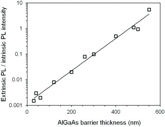
Due to the lower solubility of impurities in AlGaAs than in GaAs, they stay afloat on the AlGaAs growth surface and are progressively trapped in a thin layer (Meynadier et al., 1985) at the inverted interface upon deposition of the GaAs. The atomic scale interface roughness deduced from the linewidth measurements (Figure 7.7) are most likely due to the growth-inhibiting nature of carbon (Phillips, 1981), such as, for example, by preventing the lateral propagation of the atomic layers due to the pinning steps on the surface. This irregular structure of the interface is the source for the formation of performance and reliability-impacting defect centers. A saturation of the intrinsic FWHM PL (see Figure 7.7), equivalent to a maximum roughness detectable with the excitonic PL as an optical probe in QWs, appears to be conclusive from this model.
7.2.3.3 Prelayers for improving active layer integrity
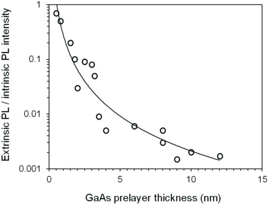
The trapping of detrimental impurity centers in the nominally undoped test QW or active QW in a diode laser can be efficiently suppressed by growing thin GaAs prelayers before the actual QW. These undesired impurities can be found in the residual MBE background atmosphere released for example during outgassing of the Al oven and shutter.
Figure 7.9 shows that the extrinsic impurity-related QW PL intensity normalized to the intrinsic exciton-related QW PL intensity can be suppressed below 1% by a GaAs SQW prelayer with a thickness of at least 5 nm. This dependence is similar to the one shown for the first time by Epperlein and Meier (1990). Similarly strong suppression can be obtained by using SL prelayers with the same total GaAs thickness. The results in Figure 7.9 are in agreement with the model of impurity incorporation described above.
Figure 7.9 Extrinsic acceptor-related PL intensity normalized to the intrinsic exciton-related PL intensity of 8 nm QWs at 2 K and 1 W/cm2 and for lower AlGaAs claddings 500 nm thick and AlGaAs barriers 30 nm thick versus the thickness of GaAs prelayers acting as impurity trapping centers. The ratio is corrected for its excitation intensity dependence. Suppression of extrinsic PL to below 1% for 5 nm and thicker GaAs prelayers. Solid line: calculated trendline.
It has been demonstrated that InGaAs/AlGaAs QW GRIN-SCH lasers with GaAs prelayers positioned in the lower AlGaAs cladding layer before the GRIN-SCH layer showed a higher efficiency and lower threshold current and, in particular, a positive effect on laser reliability compared to devices without such prelayers gettering the segregating impurities during growth.
7.3 Deep-level defects at interfaces of active regions
7.3.1 Motivation
Impurities and native defects in the crystal lattice of a semiconductor disturb the proper periodicity, which causes the formation of localized, electrically active energy states within the forbidden bandgap. Selective incorporation of dopants such as silicon or beryllium added to the semiconductor, for example, GaAs, as donors or acceptors to control the conductivity as n-type or p-type, form shallow energy levels close to the conduction or valence band, respectively.
In contrast, point defects, clusters, complexes, lattice defects, and impurities such as transition metals produce energy levels further away and are called deep-levels, traps, or nonradiative recombination centers. Deep-levels can be incorporated during device growth or processing, or both, but they can also be present in the incoming wafer material. They can have two major effects on materials and devices. Clearly, deep-levels can be either beneficial or detrimental in device manufacture. Without elaborating further, an example of the first category is the deliberate addition of deep chromium acceptors to GaAs in order to compensate the residual shallow donors to produce very high-resistivity material known as semi-insulating GaAs, which is used as the wafer substrate for electronic devices such as field-effect transistors.
More importantly in the context of this text, however, are the undesirable deep states unintentionally introduced into the laser device. There they can reduce the minority carrier lifetime by acting directly as recombination centers or by increasing the probability of Auger processes, or they can form the seed for the growth of extended dislocation networks. These effects impact the quantum efficiency and threshold current and the degradation properties, which can occur already at very low defect concentrations well below 1015 cm−3 depending on the efficiency of the trap carrier capture rate. Therefore, the need to detect and monitor deep-levels is indispensable and will grow as devices become more sophisticated and as manufacturing becomes increasingly dependent on removing the last traces of undesirable deep-levels.
It has long been established that the localized states of deep-level imperfections in the depletion region of semiconductor devices can be characterized by measuring the capacitance (or current) transients after excitation with a bias pulse or light pulse. A technique, which detects and characterizes very low concentrations of electrically active defects down to 109 atoms/cm3 is deep-level transient spectroscopy (DLTS). It has developed from the laborious single-shot transient recordings into the ingenious automation of the transient measurements and spectroscopic survey technique with inherent higher resolution due to signal averaging (Lang, 1974). Compact, commercial turnkey instruments (e.g., SEMILAB Ltd, 2012) available today are designed for measuring deep-levels including their parameters such as energy level, capture cross-section, concentration, and for profiling their spatial density in the depletion zone of a p–n junction or Schottky barrier.
In the following sections, the operating principle of the DLTS technique including a block diagram and two measurement examples are discussed. One is on the formation of deep electron traps at the upper interface of n-AlGaAs/GaAs SQWs and the other deals with the generation of a deep-level when etching the ridge waveguide of a diode laser down to close proximity to the active layer.
7.3.2 Experimental details
Figure 7.10 contains a schematic representation of the development of the capacitance transient due to a majority carrier trap in a one-sided p+–n diode. A majority (minority) carrier trap can be an electron trap in an n(p)-type material with the electron emission rate en much greater than the hole emission rate ep or a hole trap in a p(n)-type material with the hole emission rate ep much greater than the electron emission rate en. To establish conditions for unique interpretations of DLTS spectra, the junction has to be one-sided, so that the depletion zone is located predominantly at one side of the junction. Therefore, the p+–n diode configuration in the figure can detect majority electron traps and minority hole traps in the n-layer of the junction.
Figure 7.10 Schematic representation of the DLTS principle of operation for a majority electron trap in a one-sided p+-n diode. (a) Reversed-biased diode leads to depletion zone mainly in the n-layer and in this space-charge region trap states are empty of carriers (electrons) (t < 0 quiescent state). (b) During forward-biased majority carrier pulse the space-charge region collapses and traps capture carriers (electrons) (t = 0 state). (c) Upon turning off the filling pulse quickly (compared to trap emission time) change in capacitance is negative (positive for minority carrier traps), capacitance transient begins (t = 0+), reverse bias re-establishes, and capacitance transient decays due to thermal carrier emission from traps (t > 0) and proceeds until traps are empty.

The DLTS measurement sequence starts with reverse biasing the junction to generate the depletion zone (Figure 7.10a). It then works by processing the capacitance transient signal resulting from the presence of deep-levels in the depletion layer. The transient is excited by applying repetitive bias pulses in the forward direction. Alternatively, light pulses can be applied. During the forward bias pulse the deep-levels (here electron traps) will fill with electrons, because the depletion layer width shrinks (Figure 7.10b). Upon turning off quickly the forward filling pulse (compared to electron emission time), the depletion layer expands by thermal emission of electrons from the traps leaving behind the positively ionized defects (Figure 7.10c), which increases the space-charge density and is key to the DLTS measurement. Under the constant reverse bias voltage condition, this causes the diode capacitance to increase. Defect parameters such as energy level and concentration can be deduced from this capacitance transient. Compared to the velocity of free electrons, the emission rate of the electrons from the traps is relatively slow, depending on the specific nature of the trap, but most importantly it is very sensitive to temperature.
As already discussed in the previous section, the major strength of the DLTS technique is that it processes the capacitance transients in a way that yields a spectral output, that is, one capacitance peak for each deep level. This is accomplished by sampling the capacitance transient at two points in time t1 and t2 at least and by averaging the capacitance difference ΔC between these two points over many repetitions of the pulse, which finally is the basic output of the DLTS system. The capacitance meter has to respond faster than the deep-level and it has to be gated-off during the pulse to avoid overloading. By slowly varying the sample temperature while maintaining the same pulse sequence and sampling points, the output ΔC sweeps through a peak. This occurs at the temperature where the time constant set by the sampling times t1 and t2
(7.1) ![]()
matches the emission time constant of the deep-levels, 1/en. Or equivalently, when the electron trap emission rate toward the conduction band
is equal to the electronically set and adjustable rate window ![]() . Equation (7.2) is written in a simplified form where σn is the electron capture cross-section of the trap, Nc the free electron density in the conduction band, vn,th the average electron thermal drift velocity, Ec the conduction band edge energy, ET the energy level of the trap, and Ea,T = Ec − ET is the activation energy of the trap. Figure 7.11 shows schematically the various stages in the development of the final DLTS spectral signal.
. Equation (7.2) is written in a simplified form where σn is the electron capture cross-section of the trap, Nc the free electron density in the conduction band, vn,th the average electron thermal drift velocity, Ec the conduction band edge energy, ET the energy level of the trap, and Ea,T = Ec − ET is the activation energy of the trap. Figure 7.11 shows schematically the various stages in the development of the final DLTS spectral signal.
Figure 7.11 Development of the DLTS signal for a majority carrier trap. (a) Capacitance transients for different temperatures. (b) Arrhenius plot illustrating the meaning of the user-defined and adjustable rate window to match the thermal emission rate at the DLTS signal peak (c).

The emission prefactor in Equation (7.2) is temperature dependent and in a simplified form is proportional to T2 because vn,th ∝ T1/2 and Nc ∝ T3/2 where σn = σn(T) is dependent on the type of capture, which is usually unknown and therefore omitted here. By plotting ln(en/T2) versus 1/T (Arrhenius plot) we can determine the activation energy of the trap from the slope.
A capacitance DLTS temperature scan can distinguish between the types of carrier traps involved. For example, the spectral peaks are directed downward for majority electron traps in n-type material with ΔC(t) ∝ −nT(t) the density of filled electron traps, and directed upward for minority hole traps in n-type material with ΔC(t) ∝ pT(t) the density of filled hole traps.
Further types of the DLTS technique along with their relevant features are as follows:
- Isothermal capacitance DLTS: Frequency (rate window) scanned at constant temperature; for details and advantages see paragraph below.
- Current DLTS: Transient current signals; suitable for very small capacitance devices (<1 pF); more sensitive than capacitance DLTS for faster transients; no distinction between majority and minority carrier traps, I(t) ∝ ennT(t), I(t) ∝ eppT(t).
- Scanning DLTS: Pulsed electron beam (SEM) fills deep levels with carriers; two-dimensional mapping of deep levels with high spatial resolution.
- Optical DLTS: Uses pulsed bandgap light to inject electron–hole pairs; can detect minority carrier traps with Schottky diodes; extends DLTS to high-resistivity semiconductors; use of sub-bandgap light (cw) to photoionize mid-gap levels to prevent carrier freeze-out at low temperatures.
- Constant capacitance DLTS: Voltage transient; particularly applicable for high trap densities > shallow dopant concentrations.
- Double-correlated DLTS (DDLTS): Uses two filling pulses of different forward voltages; signal difference yields trap concentration in a thin layer of depletion layer; for spatial trap concentration profiling.
In practical, commercial systems the averaging is done by a double box-car integrator or by a broadband lock-in amplifier. The box-car signal averaging principle uses only a small portion of the actual capacitance transients, hence the signal to noise is far from the optimum value. Another disadvantage is that the DLTS peak amplitude will remain constant only at selected discrete values of t1 and t2. Since physical reasons might lead to changing peak heights, for example, strongly temperature-dependent capture cross-sections, to assure proper evaluation, only preselected rate windows, typically 8 to 12, are provided in box-car systems.
The lock-in averaging method (SEMILAB Ltd, 2012), however, overcomes these difficulties. It is the generalization of the box-car averaging with gate widths corresponding to half of the repetition time. However, to realize this generalization special lock-in phase-setting procedures and signal gating are necessary. A certain gate-off period has to be applied to avoid overloading the capacitance meter and the lock-in amplifier. During the excitation pulse the input to the capacitance meter is temporarily blocked. After termination of the pulse, the input is reopened, but the capacitance meter now requires a certain settling time. This is achieved in the second portion of the gate period. It is a constant fraction of the repetition time, hence the phase of the lock-in amplifier is independent of the repetition rate. This fundamentally new idea made it possible to use the theoretically more favorable lock-in amplifier in practice (Ferenczi et al., 1984). Due to the repetition rate independent phase-setting principle, the repetition rate of the lock-in amplifier can be selected continuously over four orders of magnitude instead of a few discrete rate-window settings allowed by the box-car method. It can be shown (Ferenczi et al., 1986) that the output signal of the lock-in amplifier is a function of temperature and repetition time. The function for the lock-in output signal has a maximum repetition time at fixed temperature just as it has a maximum temperature at fixed repetition time. The latter case represents the well-known temperature scan DLTS, whereas the former is the isothermal DLTS approach called frequency scan DLTS (sweeping the rate window or repetition rate). It should be noted that the temperature dependence is exponential and the frequency dependence is linear, and hence a much wider range should be scanned in frequency than in temperature to cover the same activation energy interval. With an automatic lock-in reference frequency sweep feature built into commercial systems (SEMILAB Ltd, 2012) the DLTS signal is measured typically at 1024 different frequencies covering four decimal orders.
Frequency scan DLTS has some fundamental advantages over the temperature scan approach: it avoids thermal annealing of the sample; it has better establishment of the accurate sample temperature and hence more accurate peak position determination; temperature-dependent phenomena such as basic sample capacitance or capture process do not interfere with the measurement of the trap emission rate; it is much faster because it is done electrically; and it is suitable for wafer mapping by coupling the system to an automatic wafer mapping setup.
Figure 7.12 shows a block diagram of the essential components of a standard temperature-scanned DLTS system. Most of the components have already been introduced above and their functions will be summarized briefly as follows: the temperature of the reverse-biased device under test (DUT) is ramped up typically between 77 and 420 K; the pulse generator supplies the train of voltage pulses to the sample; the capacitance meter measures the static capacitance and dynamic capacitance transient response of the sample; the capacitance transients are fed after amplification and digitization in an analog/digital (A/D) converter into the computer for signal processing; the temperature controller measures and controls the temperature in the cryostat and supplies the digitized data to the computer; the pulse generator triggers through a connections card the digitization process of the transient; and all functions including DLTS vs. T, V vs. t, C vs. t, C vs. V, etc., can be displayed on the monitor.
Figure 7.12 Block diagram of a capacitance DLTS system. To enhance sensitivity an automatic capacitance compensator is provided in the SEMILAB system, which compensates the variation of the static sample capacitance with temperature and hence keeps the fast capacitance bridge with a response time <5 μs in balance.

7.3.3 Discussion of deep-level transient spectroscopy results
In the following, we want to discuss two typical examples demonstrating the formation of growth-induced and processing-induced deep levels. The first case deals with the generation and accumulation of deep-levels under nonoptimum growth temperature conditions at the upper interface of AlGaAs/GaAs SQW structures, whereas the second case discusses the formation of a deep-level in the active region of a ridge laser, when the ridge waveguide is etched down too close to the active layer.
Nonradiative carrier recombination in the active region, at the interfaces, and in the wide-bandgap cladding regions of diode lasers is one of the major limiting factors to achieving low threshold current densities and high quantum efficiencies. To identify the responsible deep-levels and laser degradation mechanisms, DLTS measurements have been performed both on DH and SQW lasers (Uji et al., 1980; Hamilton et al., 1985; Debbar and Bhattacharya, 1987; As et al., 1987, 1988).
Figure 7.13 shows a capacitance DLTS spectrum recorded from the upper AlGaAs cladding layer of an n-AlGaAs/GaAs SQW device. The samples were originally designed to study deep-level emission effects in QW structures. They consisted of a GaAs SQW 3–40 nm wide embedded in an upper n-AlxGa1−xAs layer 100 nm thick and a lower n-AlxGa1−xAs layer (x = 0.24–0.39) 350 nm thick Si-doped to 4×1017 cm−3 and were MBE grown on an s.i. GaAs substrate with a suitable buffer consisting of a GaAs layer and AlGaAs SL (As et al., 1988). The depletion zone was generated by using a Schottky diode formed on top of the device structure and consisted of a (Ti, Pt, Au) Schottky contact and an annealed (Au, Ge, Ni) Ohmic contact. Since the zero-voltage depletion width was smaller than 100 nm, the distance to the QW, it was possible to sweep the depletion edge through the QW. The spatial resolution was determined by the Debye length and was typically 8 nm.
Figure 7.13 DLTS spectrum recorded from the upper AlGaAs cladding layer of an n-AlGaAs/GaAs SQW device sampled by a Schottky diode at a reverse bias of −3.5 V, filling pulse amplitude of +0.5 V, and a rate window of 278 s−1. (Data adapted in amended form from As et al., 1988.) E1–E6: majority electron traps.
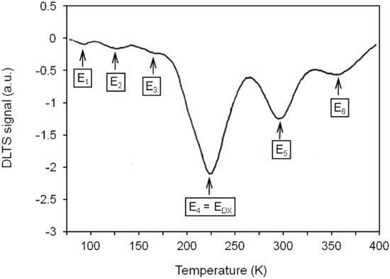
The spectrum in Figure 7.13 was taken at a reverse bias of −3.5 V, forward voltage pulses 10 μs wide of +0.5 V height, and a rate window of 278 s−1. It shows six peaks directed downward, which indicates, as discussed above, that they are generated from the emission of majority electron traps. Their T2-corrected thermal activation energies were obtained from ln(en/T2) versus 1/T plots and range between 0.12 and 0.63 eV.
At lower (0 V) and higher (−5.5 V) reverse voltages and the same 0.5 V forward voltage pulses, there is only the dominating center peak, which can be ascribed to the well-known, so-called DX center, a relatively deep donor state related to the presence of a simple substitutional donor impurity in AlxGa1−xAs (x > 0.22) and that controls the electrical properties of this material (Mooney, 1990; Ghezzi et al., 1991). This feature is characteristic of spatially localized defects. The deep levels (E1–E3, E5, and E6) in addition to the DX center have been extensively investigated by Yamanaka et al. (1987) and are in general very dependent on the growth ambient, growth temperature, and group V/III flux ratio. By determining the depth distribution of these traps the actual root cause for the formation of these traps could be revealed.
Figure 7.14 shows the depth profile of the E6 trap concentration obtained from DDLTS measurements performed at a rate window of 2787 s−1 and 0.1 V voltage difference between the two trap filling pulses. It clearly exhibits a maximum concentration in the upper AlGaAs layer at a depth of 88 nm with a FWHM of 13 nm just above the QW 3 nm wide located 100 nm below the surface. Similar distributions have been obtained for all the other additional traps with FWHM values between 12 and 26 nm. Maximum trap concentrations are high, in the order of 5×1015 cm−3, as calculated by convoluting the DDLTS depth signal with the C/V profile carrier concentration measured during the majority carrier pulse (Lang, 1974; As et al., 1988).
Figure 7.14 Depth profile of trap concentration of trap E6 (see Figure 7.13) obtained by DDLTS with amplitude difference between the two excitation pulses ΔV = +0.1 V, pulse duration 300 μs, rate window 2787 s−1. The same distribution was obtained for the other traps E1–E3 and E5. Position of the 3 nm wide QW is indicated for comparison. (Data adapted in amended form from As et al., 1988.)

The origin of the defects may be due to the nonoptimum growth condition for the first 10–20 nm of the AlGaAs layer. In this region the substrate temperature of 680 °C is too low for defect-free growth. Yamanaka et al. (1987) have shown that deep traps with comparable activation energies are observed if the growth temperature is below 715 °C. The time to stabilize to the optimum temperature of 715 °C is equal to the time to grow about 25 nm, which agrees well with the FWHM of the trap distributions observed. Since for the lower AlGaAs growth the optimum substrate temperature was kept constant up to the start of the GaAs growth, no defects were observed (cooling-down time for GaAs growth is much quicker than heating-up time for upper AlGaAs).
An interrupted growth after the GaAs QW would allow the resumption of optimal AlGaAs growth conditions and would most likely prevent the formation of these detrimental deep states, which are in contrast to the DX centers mainly responsible for the degradation of the PL efficiency in MBE-grown AlGaAs layers and the performance of AlGaAs/GaAs QW lasers (Yamanaka et al., 1984, 1987; Bhattacharya et al., 1984).
The second example describes the formation of a deep trap in the etching process of ridge waveguide InGaAs/AlGaAs SQW GRIN-SCH lasers. The DLTS spectrum of a laser device with an etched ridge depth of 1.5 μm, equivalent to a 0.5 μm residual thickness, which is the distance from the bottom of the etch to the active layer, is displayed in Figure 7.15a and shows only the dominating DX center complex (typically 1018 cm−3), which is known to have no impact on optical properties (Yamanaka et al., 1984). In this case, the etching is not interfering with the p–n junction of the diode and these lasers show no abnormal degradation behavior.
Figure 7.15 DLTS spectra of ridge waveguide InGaAs/AlGaAs GRIN-SCH SQW diode lasers recorded at a reverse bias of −3 V, filling pulse width of 20 μs, and rate window of 250 s−1. (a) Laser with large residual thickness between bottom of wet-etched ridge and active layer. (b) Laser with low residual thickness inducing deep majority carrier trap in addition to DX defect center, which is known to be inherent in Si-doped bulk n-AlGaAs.

In contrast, ridge lasers deeply etched down to about 1.9 μm leaving a residual thickness of ![]() 0.1 μm show a distinct additional peak in the DLTS spectrum, which can be attributed to majority carrier trap emission (Figure 7.15b). In principle, this additional majority carrier trap could be either an electron trap in the n-type material or a hole trap in the p-type material of the junction. However, the presence of the DX peak in the same spectrum indicates that it is more likely an electron trap in the n-layer.
0.1 μm show a distinct additional peak in the DLTS spectrum, which can be attributed to majority carrier trap emission (Figure 7.15b). In principle, this additional majority carrier trap could be either an electron trap in the n-type material or a hole trap in the p-type material of the junction. However, the presence of the DX peak in the same spectrum indicates that it is more likely an electron trap in the n-layer.
The symmetry of the p–n junction leading to an extension of the depletion zone into the n- and p-layers in principle did not allow unique identification of the traps (apart from DX which is linked to n-type Si-doped AlGaAs). As the doping levels in the symmetrical p–n junction of the diode are high, the depletion zone could be extended to a maximum width of only ±0.15 μm with the available maximum reverse bias voltage. However, it was sufficient to probe the GRIN-SCH region width and DDLTS showed that the trap is located at the interfaces of the GRIN-SCH layer to the surrounding cladding layers, laterally predominantly effective at the lower corners of the ridge waveguide where it can have a strong impact, particularly on laser reliability. It has been demonstrated that the trap, which is very efficient due to its high activation energy of ![]() 0.8 eV and concentration, can lead to rapid failure of the diode laser.
0.8 eV and concentration, can lead to rapid failure of the diode laser.
7.4 Micro-Raman spectroscopy for diode laser diagnostics
7.4.1 Motivation
Raman spectroscopy is a very effective spectroscopic technique for studying the interaction between monochromatic light and matter, in which the light is inelastically scattered (Raman, 1928; see, e.g., Balkanski, 1971; Cardona and Güntherodt, 1975–91). It has become a very important and highly versatile analytical and research tool, which can be used for fast, nondestructive chemical and structural analyses of solid, liquid, and gaseous matter in industrial and research applications as wide ranging as pharmaceuticals, forensics, chemistry, material science, and, above all, semiconductors. As the inelastically scattered light has interacted with the fundamental atomic and molecular excitations of the matter, it carries a wealth of information and all the crucial data necessary to characterize the microscopic properties and status of the matter, which finally show up, in effect as a fingerprint, in a Raman spectrum.
Figure 7.16 shows a schematic overview of the Raman effect including relevant Raman signal parameters and Raman interactions in semiconductors. It shows the Raman backscattering or near-backscattering configuration, which is widely used on opaque materials such as semiconductors. The small penetration depth of light of typically 100 nm in semiconductors such as GaAs permits the study of very thin layers. Within the topic of this text, we are especially interested in the signal parameters of energy and intensity and in the inelastic light scattering process with optical phonons yielding information on composition, structure, lattice disorder, strain, and temperature of the material and device.
Figure 7.16 Schematic overview of the Raman inelastic light scattering process on the opaque semiconductor sample in backscattering geometry. Also shown are relevant signal parameters and interactions with elementary excitations in a semiconductor. Terms highlighted in bold are major subject topics in this text. (Parts adapted in modified form from Brugger, 1990.)

This section deals predominantly with local temperatures at laser facets measured in dependence on laser output power, applied mirror technology, laser material, vertical laser structure, and laser chip mounting technique. In Chapter 8 next, we use Raman to reveal and characterize the microscopic root causes of enhanced mirror temperatures, strain along the active layer on the facet of ridge laser devices, and the instability of the mirror coating material by recrystallization under high laser output power.
But first we discuss briefly the physical fundamentals of the Raman effect, the Raman scattering configuration and phonon modes on a standard laser facet, the expression used to calculate the mirror temperature from the Raman spectrum, and finally some experimental details and results.
7.4.2 Basics of Raman inelastic light scattering
The Raman effect is based on the molecular polarizability of the material which is determined by deformations of the molecules in the material by the oscillating electromagnetic wave of the incident light. An electric dipole moment equal to the product of polarizability and electric field is subsequently induced, and the molecules start vibrating (and rotating in a gas or liquid) with a characteristic frequency ![]() due to the periodic deformation. Monochromatic laser light with frequency
due to the periodic deformation. Monochromatic laser light with frequency ![]() excites molecules and transforms them into oscillating (and rotational) dipoles, which can emit light at three different frequencies.
excites molecules and transforms them into oscillating (and rotational) dipoles, which can emit light at three different frequencies.
As already indicated in Figure 7.16, photons interacting with the molecules of the material scatter elastically and inelastically. The former process is called elastic Rayleigh scattering where the scattered photons have the same frequency ωr = ωi as the incident light. In this case, the molecule has no Raman-active mode and absorbs a photon with frequency ωi, and the excited molecule returns to the same basic excitation, which in a solid can be, for example, a vibrational (phonon) mode.
However, only one out of about 1012 photons is inelastically scattered. This can be obtained by assuming a typical Raman scattering efficiency per unit length x and unit solid angle ![]() as low as
as low as
(7.3a) ![]()
where I is the Raman scattering efficiency of the Stokes or anti-Stokes Raman line in the spectrum (see below), ![]() is the solid angle, and x the coordinate of the light into the sample. By using a typical penetration depth of 10−5 cm for the excitation light, for example, in GaAs, the total efficiency can be written as
is the solid angle, and x the coordinate of the light into the sample. By using a typical penetration depth of 10−5 cm for the excitation light, for example, in GaAs, the total efficiency can be written as
(7.3b) ![]()
which means that only one photon out of 1012 is inelastically scattered! This extremely low generation probability of Raman photons requires the use of an extremely efficient detection system and the removal of any stray light and Rayleigh background light (see next sections), which might hinder greatly the Raman light detection. The Raman signal is proportional to
(7.3c) ![]()
with σ the scattering cross-section, n(![]() ) the scatterer concentration, and V the scattering volume.
) the scatterer concentration, and V the scattering volume.
The energy of the Raman light is shifted either lower or higher (red or blue shift, respectively). It is the change in energy which provides the chemical and structural information.
Red-shifted photons are the most common, because at room temperature the population is principally in the molecule's ground state (vibrational, rotational, or electronic level), and therefore the Raman scattering effect is larger. Upon interaction with the photon, the molecule is excited into a higher virtual state, part of the incident photon's energy is transferred to the Raman active mode with frequency ![]() , and the resulting frequency of the scattered light is reduced to ωi −
, and the resulting frequency of the scattered light is reduced to ωi − ![]() , called the Stokes shift. The loss of energy is directly related to the functional group bonds, the structure of the molecule to which it is attached, the types of atoms in that molecule, and its environment. Factors such as the polarization state of the molecule determine the Raman scattering intensity, which increases with increasing change in polarizability. This means that some vibrational (phonon) or rotational transitions or transitions of any other fundamental excitations, which show low polarizability, will not be Raman active and therefore do not appear in a Raman spectrum.
, called the Stokes shift. The loss of energy is directly related to the functional group bonds, the structure of the molecule to which it is attached, the types of atoms in that molecule, and its environment. Factors such as the polarization state of the molecule determine the Raman scattering intensity, which increases with increasing change in polarizability. This means that some vibrational (phonon) or rotational transitions or transitions of any other fundamental excitations, which show low polarizability, will not be Raman active and therefore do not appear in a Raman spectrum.
On the other hand, blue-shifted photons are much less common. In this case, a photon with frequency ωi is absorbed by a Raman active molecule, which at the time of interaction is already in an excited state with higher energy. Excess energy of the excited Raman active mode is released, the molecule returns to the basic energetic state, and the resulting frequency of scattered light will be shifted to a higher frequency ωi+![]() , which is designated as the anti-Stokes shift. The processes discussed here are schematically illustrated in Figure 7.17.
, which is designated as the anti-Stokes shift. The processes discussed here are schematically illustrated in Figure 7.17.
Figure 7.17 Schematics showing fundamental Raman scattering processes. (a) Graph of Stokes and anti-Stokes scattering process. (b) Energy-level diagram for Raman scattering. Gray tone intensity indicates strength of Raman line.

Figure 7.18 shows schematically the Stokes and anti-Stokes Raman spectra in connection with the PL spectrum, which can be excited in the same process. The Raman effect, which is nonresonant, differs in general from a luminescence process, which is resonant, by exciting the material to a discrete (not virtual) energy level. This means that the Raman effect can take place actually for any energy of incident light. And the luminescence spectrum is anchored at a specific excitation energy, whereas a Raman spectral line maintains a constant separation from the excitation energy. The correct selection of the exciting laser wavelength is crucial so that the luminescence spectrum does not interfere with the Raman spectrum to such an extent that it is no longer detectable.
Figure 7.18 Schematic illustration of Raman spectra at two different light excitation frequencies ωi2 > ωi1 in relation to the PL spectrum excited simultaneously.

By using Bose–Einstein statistics for the occupation number of the elementary excitations, the intensity of the temperature-dependent Stokes (IS) and anti-Stokes (IAS) scattered light can be estimated as follows (Cardona and Güntherodt, 1975–91):
where n(![]() ) is the density of the fundamental vibrational, rotational, or electronic excitations with frequency
) is the density of the fundamental vibrational, rotational, or electronic excitations with frequency ![]() taking part in the Raman inelastic light scattering process. As we will show further below, the ratio between the integrated intensities of the Stokes and anti-Stokes optical phonon lines in the Raman spectrum will be used for calculating the sample temperature, which is already indicated in Equation (7.4c). In all further discussions, we will use phonons as the fundamental excitations taking part in the Raman process.
taking part in the Raman inelastic light scattering process. As we will show further below, the ratio between the integrated intensities of the Stokes and anti-Stokes optical phonon lines in the Raman spectrum will be used for calculating the sample temperature, which is already indicated in Equation (7.4c). In all further discussions, we will use phonons as the fundamental excitations taking part in the Raman process.
7.4.3 Experimental details
The extremely low Raman efficiencies (see above) require experimental equipment optimized in at least the following four major components:
- Monochromatic and collimated excitation source, usually a laser with selectable wavelengths.
- Optical system for producing a magnified image of microscopic areas of the sample, for focusing the laser beam onto the sample and for collecting efficiently the weak inelastically scattered radiation.
- Spectrometer system with high stray and Rayleigh light rejection ratio and high spectral resolving power for analyzing the spectral content of the inelastically scattered laser light.
- Detector with high sensitivity for detecting the extremely weak, spectrally resolved Raman light.
In Figure 7.5 we have already introduced the multipurpose optical system, which comprises also the essential components needed for generating Raman spectra on diode lasers, in particular on the laser mirrors, in a very efficient way with high sensitivity, high spectral and spatial resolution, and high stray and laser light rejection. In the following, we shall give some details of the system, which was assembled by the author from individual components.
The Ar+ laser line 457.9 nm with a low intensity of typically 1 mW and below was used throughout the Raman experiments on diode laser facets. This ensured, in combination with a high-quality 40/0.63 objective lens and xyx-translation stage with 0.1 μm resolution, the achievement of the required spatial resolution of ≤ 1 μm with negligible self-heating (ΔT < 10 K) of the laser spot on the laser die, which was attached to a heat sink. The mirror structure was observed with a video camera and monitor under high magnification of 104×. This was made possible by coupling simple lamplight from a fiber bundle via a beamsplitter into the optical path through the objective lens and onto the sample. The sample was then imaged in reverse path at a large image distance onto a camera with zoom. This procedure was used to align the sample to the laser focus. The beamsplitter was removed for the actual measurement.
To block out the laser light from detection usually commercially available interference (notch) filters are employed, which cut-off a spectral range of typically ±80–120 cm−1 from the laser line. This method may be efficient in stray light elimination, but it does not allow detection of low-frequency Raman modes in the range below 100 cm−1. However, these filters have additional severe drawbacks related to quantitative Stokes and anti-Stokes Raman spectra measurements, for example, for determining the absolute temperature at a laser facet. The drawbacks include: (i) the rejection of Rayleigh scattered light in the notch region is not sufficient; (ii) the spectral bandwidth of the notch region is not sufficiently narrow; and (iii) the edges of the notch region are not sufficiently sharp and steep. The consequences are that only Raman signals with larger energy shifts are accessible, which means that essential parts of the Raman spectrum in the low-energy regime cannot be revealed. Another drawback is: (iv) the transmission outside the notch (stopband) is not uniform and different in the Stokes and anti-Stokes energy regime of the Raman spectrum. Therefore, the spectra have to be corrected with the exact filter transmission curves for the quantitative measurements of facet temperature, which is cumbersome and not error-free. Further drawbacks are: (v) each filter is designed for only one specific probe laser wavelength; and (vi) the filters are expensive, of limited use, and not easy to handle.
The author has developed and successfully used a novel and efficient method to reject the interfering Rayleigh light from detection in Raman microprobe spectroscopy on usually (110)-oriented laser facets (Epperlein, 1992). It employs crossed polarizations of incident and scattered light in conjunction with a commercial polarizing beamsplitter (PBS), which has polarization-dependent transmissions. This new method avoids all the drawbacks listed above for notch filters.
Figure 7.19 demonstrates the basic function by using a simple PBS, which consists of a pair of right-angled prisms, cemented together, hypotenuse-face to hypotenuse-face, with a special multilayer dielectric film in between. The incident light from the excitation laser is linearly polarized (p-polarization) such that it passes straight through the cube onto the laser facet surface with the correct polarization for symmetry-allowed Raman scattering (see Section 7.4.4 and Figure 7.20 below). Upon scattering, the Rayleigh light with unchanged polarization is transmitted back through the cube. In contrast, the interesting Raman light with a polarization orthogonal to that of the incident beam (s-polarization) is reflected by the multilayer dielectric film at a 90° angle and fed into the spectrometer for spectral detection.
Figure 7.19 Schematic representation of the basic operating principle of using a polarizing beamsplitter (PBS) for effectively separating the elastically scattered Rayleigh light from the inelastically scattered Raman light before entering the spectrometer. Top view: 〈100〉 orientation perpendicular to figure plane.
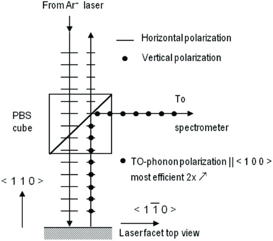
Figure 7.20 Crystal orientations in a typical (110) ridge diode laser facet.

The extinction ratio (ER) between Rayleigh and Raman light of this basic configuration is in the range of 10−2 to 10−3 at the detection input and the cut-off spectral range from the laser line is now dramatically reduced to about ±25 cm−1. By using a crossed pair of PBS cubes or a high-quality polarizing Thompson calcite prism ER can be further increased to 10−4–10−6 and Raman signals as close as ~10 cm−1 to the laser line can be detected, which is never possible with notch filters.
The requirements of the spectral detection system are enormously high considering the facts that, first, the Raman signal is many orders of magnitude weaker than the elastically scattered Rayleigh light and that, second, the difference between the Raman signal energy and laser light energy is extremely low, in the region of 1% of the laser energy. For example, 1% of the energy of the Ar+-laser 457.9 nm line amounts to 0.01×2.7 eV = 27 meV, which is a typical phonon energy in GaAs.
The spectrometer must meet stringent conditions to observe this weak sideband close to the strong laser line. It must have a high spectral resolving power Δλ/λ, which is for the double spectrometer in Figure 7.5 with a specified focus length of 0.85 m (effectively 0.9 m due to the detector column added) and dual-holographic grating greater than 104. This means that spectral structures separated by ≤0.05 nm can be resolved at an excitation laser line in the visible region.
Another stringent condition is that the stray light rejection ratio, that is, the ratio of the integrated background stray light to the signal light intensity, is sufficiently small. The specified stray light rejection ratio of the double spectrometer in Figure 7.5 is <10−14, which in combination with the use of the external PBS discussed above fully meets the requirements to perform high-performance reliable Raman spectroscopy measurements. Stray light, which is produced by imperfections in the optics and by the scattering of light at walls and dust particles inside the spectrometer, is about an order of magnitude less intense from holographic gratings than from ruled gratings. It can be further minimized by using a smooth sample surface and by flushing the spectrometer with a purified and inert purge gas such as nitrogen. This avoids negative effects such as water vapor absorption and oxygen/ozone contamination of the optics, although ozone buildup occurs only in the presence of deep UV radiation.
Finally, modern Raman systems employ single-photon counting electronics and multichannel detection systems. In the former, a discriminator selects and counts only photocurrent pulses arriving at the photomultiplier tube (PMT) anode with large enough amplitude and originating at the photocathode. The background noise or dark count rate originating from thermionic emission of electrons at the photocathode has to be kept low. This can be achieved by cooling the PMT to ~−20 °C by using a thermoelectric cooler or even to liquid nitrogen temperature of −196 °C and by selecting a PMT with a Cs-activated GaAs photocathode. The system in Figure 7.5 used a selected GaAs:Cs PMT with a low dark count rate of ~5 counts/s at the maximum anode/cathode voltage of 1800 V and had a dynamic range of >106.
The second system is an optical multichannel analyzer (OMA) using a cooled charge-coupled device (CCD) array detector. This method has the advantage of detecting and imaging a certain width of the spectrum after a given signal integration time without having to scan the spectrometer output as in the case of the PMT method. The achievable width of the spectrum depends on the spectral resolving power of the spectrometer, the exit slit width, and the width of the array. The spectral resolution, which depends also on the pixel size of the detector array, is generally lower than that in a scanning system with the same spectrometer specifications. Finally, the sensitivity of the CCD detector can be enhanced by adding an image intensifier tube. A discussion of these systems is, however, beyond the scope of this text, but we refer the interested reader to the relevant literature, for example, Chang and Long (1983).
7.4.4 Raman on standard diode laser facets
The Raman scattering event has to meet the energy and wavevector conservation laws
(7.5) ![]()
(7.6) ![]()
where K is the crystal momentum of the elementary excitation (e.g., phonon), the minus sign stands for the Stokes processes, and the plus sign for the anti-Stokes processes. The wavevectors for ki and ks of the incident (i) and scattered (s) photon, respectively, are given by 2π/λ where λ is the wavelength of the light typically in the region of 5000 Å. These wavevectors are very small compared to the large wavevectors of the phonon estimated by 2π/a0 where a0 is the lattice constant typically in the order of 5 Å. This means that only phonons very close to the center of the Brillouin zone (K = 0) can participate in the inelastic light scattering process. However, any destruction of the translational symmetry, which leads to a breakdown of the k-conservation law, for example, by lattice disorder effects, allows the participation of phonons of any K vector (K ≠ 0) in the Raman scattering process.
Figure 7.20 shows the relevant crystal orientations of a (zinc-blende semiconductor) diode laser mirror with a typical (110)-oriented facet. Raman microprobe spectroscopy is done in a backscattering configuration from the (110)-oriented facet of the opaque semiconductor surface, which means that the k vectors of the incident and scattered light are anti-parallel to each other or, in other words, the scattered light is collected by the same lens as that through which the incident light is focused.
Raman selection rules determine the existence of Raman-active phonons for certain choices of the incident and scattered polarizations and scattering geometries (for details see, e.g., Yu and Cardona, 2001). According to these, at an ideal (110) facet, scattering at transverse optical (TO) phonons is allowed by symmetry, whereas scattering at longitudinal optical (LO) phonons is symmetry forbidden. The symmetry-allowed scattering configurations written in the so-called Porto notation ki(ei, es)ks, where ki and ei are the wavevector and polarization vector of the incident light and ks and es the wavevector and polarization vector of the scattered light, respectively, can be written as
(7.7) ![]()
for the parallel-scattering geometry and
(7.8) ![]()
for the crossed-polarization configuration.
As examples, scattering at AlGaAs leads to two modes, GaAs-like and AlAs-like zone center TO phonon modes. In contrast, scattering at AlGaInP shows a one-mode behavior, that is, only one Raman AlGaInP TO phonon mode (Bayramov et al., 1981).
At real (110) facets the translational symmetry can be destroyed by structural and compositional disorder, surface electric fields, strain, or other perturbations, which results in a relaxation of the k-conservation law. As mentioned above, this allows Raman scattering at phonons of any K vector (K ≠ 0) including first-order transverse optical (TO), longitudinal optical (LO), transverse acoustic (TA), longitudinal acoustic (LA) phonons, and second-order phonons such as 2TO and 2TA.
7.4.5 Raman for facet temperature measurements
By using the ratio IS/IAS between the integrated intensities of the Stokes (S) and anti-Stokes (AS) Raman lines of the appropriate TO phonon mode in the material system under investigation, the local mirror temperature T can be determined as follows (Compaan and Trodahl, 1984):
where R is the reflectivity, α the absorption coefficient, and nr the refractive index of the facet material at frequencies ωS and ωAS. C1 is a correction factor due to the different responses of the detector and gratings at Stokes and anti-Stokes frequencies. For a backscattering geometry, R can be calculated for the Stokes and anti-Stokes light from (see also Equation 1.12)
(7.10) ![]()
where κ is the extinction coefficient. By using ellipsometry data for nr and κ (Aspnes et al., 1986) of the major materials GaAs, AlGaAs, InGaAs, and AlGaInP used in the Raman studies of this text, a typical TO phonon energy ħ![]()
![]() 33 meV, and the energy of the incident laser ħωi
33 meV, and the energy of the incident laser ħωi ![]() 2.7 eV, the total correction factor in front of the exponential term can be calculated as C1×C2
2.7 eV, the total correction factor in front of the exponential term can be calculated as C1×C2 ![]() 0.9. The temperature dependence of the S- and AS-Raman susceptibilities has been neglected in the calculations.
0.9. The temperature dependence of the S- and AS-Raman susceptibilities has been neglected in the calculations.
The sensitivity of T on IS/IAS was calculated on the basis of Equation (7.9) by using the values of the phonon energy and correction factor in the previous paragraph. Figure 7.21 shows that a ±5% error in a typical value 2.5 for IS/IAS leads to a roughly ±20 K error in temperature of 375 K corresponding to IS/IAS = 2.5. Of course, at higher IS/IAS values the error in temperature is lower, whereas at lower values it is much higher. The IS/IAS intensity ratio is very insensitive to temperature changes at high-temperature levels, which hampers accurate temperature measurements.
Figure 7.21 Calculated sensitivity of the mirror temperature T on the Stokes/anti-Stokes intensity ratio IS/IAS of a suitable phonon mode in the Raman spectrum; ħ![]() = 33 meV is used for the GaAs TO phonon and 0.9 for the total correction factor in the calculation.
= 33 meV is used for the GaAs TO phonon and 0.9 for the total correction factor in the calculation.
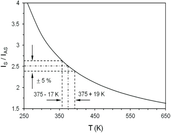
7.4.5.1 Typical examples of Stokes- and anti-Stokes Raman spectra
Figure 7.22 shows typical examples of AS- and S-Raman spectra of a cleaved, uncoated facet of an AlGaAs/GaAs GRIN-SCH SQW laser 3 μm wide (Brugger and Epperlein, 1990). The probe laser was focused on the optical near-field spot. The upper curves were taken from the nondegraded laser at a cw power of 5 mW per facet. The spectra, detected in symmetry-allowed, parallel-scattering configuration, show the first-order GaAs-like and AlAs-like TO phonon modes, as expected. The spectra show the typical two-mode behavior in contrast to AlGaInP with a one-mode spectrum, as we will show in the next example below. The Ar+-ion laser plasma line recorded in the spectra can be used as a very useful energy reference for measurements of very accurate frequency shifts and to obtain qualitative information on changes in surface roughness via intensity fluctuations of the elastically scattered Rayleigh light (see also Section 8.1).
Figure 7.22 Raman spectra of a cleaved, uncoated (110) facet in the near-field (NF) of an (Al)GaAs GRIN-SCH SQW ridge laser 3 μm wide during operation: (a) 5 mW per facet, laser not degraded; (b) 18 mW per facet, laser degraded. (Parts adapted in modified form from Brugger and Epperlein, 1990.)

The lower curves in Figure 7.22 were recorded from the same mirror region and at the same low excitation intensity of ![]() 100 kW/cm2 (leading to a temperature rise <10 K), but after heavy degradation of the laser with a strong increase in threshold current. The laser was here operated at 18 mW/facet resulting in a significant heating of the facet. This can be seen in a shift of the phonon lines to lower energies and broadening of the linewidths caused by anharmonic effects in the crystalline material. However, most importantly, the S/AS intensity ratio is decreased with the higher temperature. The absolute intensities of the AS and S signals are also higher due to the temperature-dependent change of the Bose–Einstein occupation number (Equations 7.4a, 7.4b), optical material constants, and the resonance curve of the Raman susceptibility (Compaan and Trodahl, 1984). The line at 195 cm−1 can be attributed to a disorder-activated (DA) phonon mode. Its existence demonstrates strong crystal damage at the facets of the degraded laser. We discuss this mode in detail in the context of revealing the microscopic root causes of enhanced facet temperatures and linked COMD probability (see Section 8.1).
100 kW/cm2 (leading to a temperature rise <10 K), but after heavy degradation of the laser with a strong increase in threshold current. The laser was here operated at 18 mW/facet resulting in a significant heating of the facet. This can be seen in a shift of the phonon lines to lower energies and broadening of the linewidths caused by anharmonic effects in the crystalline material. However, most importantly, the S/AS intensity ratio is decreased with the higher temperature. The absolute intensities of the AS and S signals are also higher due to the temperature-dependent change of the Bose–Einstein occupation number (Equations 7.4a, 7.4b), optical material constants, and the resonance curve of the Raman susceptibility (Compaan and Trodahl, 1984). The line at 195 cm−1 can be attributed to a disorder-activated (DA) phonon mode. Its existence demonstrates strong crystal damage at the facets of the degraded laser. We discuss this mode in detail in the context of revealing the microscopic root causes of enhanced facet temperatures and linked COMD probability (see Section 8.1).
In contrast, Figure 7.23 illustrates the one-mode Raman spectrum of (Al)GaInP. It shows the first-order Stokes and anti-Stokes spectra of a nondegraded facet of an unbiased AlGaInP/GaInP GRIN-SCH MQW ridge laser 5 μm wide detected in symmetry-allowed, crossed-polarization geometry (Epperlein et al., 1992). The focused (~1 μm), low-power (1–2 mW) probe laser beam irradiated part of the near-field region and part of the GaAs substrate. With this probing condition the temperature gradient expected between the hot (Al)GaInP regions and the GaAs substrate could be evaluated in one spectrum recorded at different drive currents and power levels (see next section). The spectra show the GaAs substrate TO phonon mode well separated from the (Al)GaInP TO phonon peak exhibiting the widely accepted one-mode behavior of AlGaInP. The peak appearing as a shoulder at ±350 cm−1 on the high-energy side of this peak can be attributed to one-phonon optical transitions due to disorder in the crystal structure (Bayramov et al., 1981).
Figure 7.23 Raman spectra of a cleaved, uncoated (110) mirror facet of an unbiased (Al)GaInP GRIN-SCH MQW ridge laser 5 μm wide on a GaAs substrate. Excitation laser spot in parts on near-field pattern and in parts on GaAs substrate. (Parts adapted in modified form from Epperlein et al., 1992.)

7.4.5.2 First laser mirror temperatures by Raman
Figure 7.24 shows mirror temperature ΔT versus power P calculated from Stokes- and anti-Stokes GaAs-like TO phonon modes of cleaved uncoated and coated AlGaAs/GaAs lasers with different ridge widths (Brugger and Epperlein, 1990; Brugger et al., 1990). The temperature data consider the small temperature increases due to self-heating of the low-power excitation laser (see previous section). The temperature increase ΔT is relative to the temperature at threshold current with P ![]() 0. The narrower the ridge, the higher are the temperatures due to the higher power densities and the more pronounced is the nonlinear ΔT/P dependence.
0. The narrower the ridge, the higher are the temperatures due to the higher power densities and the more pronounced is the nonlinear ΔT/P dependence.
Figure 7.24 Measured temperature rises ΔT at mirror facets inside the near-field spot of (Al)GaAs GRIN-SCH SQW lasers as a function of cw optical output power P: (a) 3 μm wide ridge, cleaved and uncoated mirror; (b) 8 μm wide ridge, cleaved and uncoated mirror; (c) 8 μm wide ridge, cleaved and passivation-coated Al2O3 mirror λ/2-thick. Solid/dashed lines are guides to the eye. (Data adapted in modified form from Brugger and Epperlein, 1990.)

Typical values for cleaved uncoated mirrors are ΔT > 100 K for P > 5 mW per 1 μm ridge width. Once degradation has occurred, a continuous increase of ΔT can be observed as a function of time at constant P (not shown; see also critical facet temperature to COMD event in Chapter 9). ΔT can go up to 103 K on highly degraded uncoated mirrors. On the other hand, passivation-coated mirrors with transparent Al2O3 layers λ/2-thick show temperatures strongly reduced by about a factor of 10 compared to cleaved uncoated devices with the same widths (Figure 7.24c). These optical thicknesses of λ/2 lead to no interference losses and leave the reflectivity at about 30%, the value for cleaved uncoated GaAs mirrors. The degradation threshold of these laser facets is about five times higher than for uncoated ones, which can be ascribed to the passivation of dangling bonds at the cleaved surface and therefore a reduction of effective nonradiative recombination centers and surface recombination velocity, as discussed in Chapter 4.
The next two figures show ΔT as a function of the drive current Id and power P for cleaved uncoated facets of (Al)GaInP GRIN-SCH MQW ridge lasers 5 μm wide (Epperlein et al., 1992).
The temperatures in Figure 7.25 were obtained from the S/AS intensity ratios of the (Al)GaInP TO phonon peak and GaAs substrate TO phonon mode of the spectra as described in Figure 7.23. The ΔT data comprise data obtained for two nearly identical lasers and allow for the low heating effect (~10 K) of the low probe laser power ~1 mW.
Figure 7.25 Measured temperature rises ΔT at cleaved uncoated facets of two ridge (Al)GaInP GRIN-SCH MQW lasers 5 μm wide as a function of drive current Idrive: (a) temperature in (Al)GaInP near-field spot; (b) temperature in GaAs substrate near GaAs/AlGaInP interface. Solid/dashed lines are guides to the eye. (Data adapted in modified form from Epperlein et al., 1992.)

There are clearly two regimes indicating different heating mechanisms. Below threshold in the spontaneous emission region, ΔT increases to a maximum of ~35 K, a value which agrees well with the bulk temperature rise of the active p–n junction region along the cavity axis as found from the comparison between P/Id characteristics recorded under pulsed and dc conditions. In this regime, ΔT is caused by Joule heating of Id. Above threshold, ΔT rapidly increases with Id reaching ~100 K at 1.5Ith. Here, the Joule heating effect is superimposed by heating due to absorption of laser radiation, which leads to an enhanced nonradiative surface recombination.
The low ΔT values in the lower branch of Figure 7.25, measured in the GaAs substrate close (<1 μm) to the epilayer/substrate interface, indicate a steep temperature gradient in the direction perpendicular to the active layer. This is more pronounced than what is known from temperature maps of AlGaAs/GaAs laser mirrors (Epperlein, 1993; see Chapter 9) due to the higher thermal resistivity of AlGaInP (Adachi, 1983).
This thermal behavior is more distinct in the ΔT versus P plots in Figure 7.26 where the slope of the curves in the lasing regime is indicative of the thermal resistivity. The slope ratio of ~6 is in reasonable agreement with the known ratio between the thermal resistivities of the used composition (Al0.7Ga0.3)0.52In0.48P and GaAs. The ΔT data are in good agreement with independent measurements using the Raman phonon line energy shift (Epperlein et al., 1992) and thermoreflectance as a novel approach for laser mirror characterization (Epperlein, 1993; see Chapter 9). The data demonstrate the high heating efficiency of the (Al)GaInP facets with ΔT > 100 K for 0.8 mW lasing power per 1 μm ridge width and therefore pose a high risk for laser reliability.
Figure 7.26 Measured temperature rises ΔT at cleaved uncoated facets of two ridge (Al)GaInP GRIN-SCH MQW lasers 5 μm wide as a function of cw power P: (a) temperature in (Al)GaInP near-field spot; (b) temperature in GaAs substrate near GaAs/AlGaInP interface. Solid/dashed lines are guides to the eye. (Data adapted in modified form from Epperlein et al., 1992.)

7.4.6 Various dependencies of diode laser mirror temperatures
The next three sections deal with the dependence of mirror temperatures on laser material, mirror surface treatment, number of active QWs, cladding layer material, use of a heat spreader, and type of mounting the laser die on a heat sink. Further dependencies such as on a bent-waveguide nonabsorbing mirror structure and the type of mirror passivation technology will be discussed in Chapters 8 and 9, and also in connection with the novel thermoreflectance measurement technique pioneered and introduced successfully by the author as a fast and highly versatile technique for diode laser characterization (Epperlein, 1993).
7.4.6.1 Laser material
The dependence of ΔT on laser material is shown in Figure 7.27. For clarity, the mirror temperatures of cleaved uncoated SQW ridge lasers 5 μm wide are plotted (Epperlein, 1996). They are higher for (Al)GaInP lasers than for (Al)GaAs lasers primarily because of the relatively high thermal and electrical resistivity of AlGaInP cladding layers. The low mirror temperatures of the compressively-strained AlGaAs/InGaAs lasers are predominantly due to low bulk and surface defect densities. It is worth mentioning that EBIC studies (Jakubowicz and Fried, 1993) on strained lasers showed that, in terms of defect formation, the strained active QW can effectively screen the ridge-induced strain fields (Epperlein et al., 1990, 1995). This can reduce the generation and migration of defects at the mirrors during laser operation resulting in lower facet heating and hence higher mirror stability and laser performance. It may also be supported by the fact that we never observed the discontinuity at threshold in the ΔT/Id plots of nondegraded AlGaAs/InGaAs lasers. However, upon moderately degrading these lasers at the mirror surface, which appeared as an increase in Ith, the kink at Ith then appeared and the temperatures increased by a factor of ~4 (see Chapter 9). This kink at threshold was always observed for all the other laser types investigated. Based on this information, a laser structure can be designed with minimum mirror heating and hence increased power level at COMD.
Figure 7.27 Temperature increases ΔT at cleaved uncoated facets inside the near-field of (Al)GaInP, (Al)GaAs, and AlGaAs/InGaAs GRIN-SCH SQW ridge lasers 5 μm wide as a function of cw power P. Solid lines: calculated trendlines.

7.4.6.2 Mirror surface treatment
Figure 7.28 plots the mirror temperature increases ΔT versus the optical power P for different mirror treatments of (Al)GaAs GRIN-SCH SQW ridge lasers 7 μm wide. The temperatures are highest for cleaved, untreated, and uncoated mirrors. They can be reduced by an oxygen-plasma ashing process usually applied to remove residual photoresist from an etched mirror structure and the deposition of a Si3N4 coating layer λ/2 thick. The removal of the damage layer formed after the oxygen-ashing treatment by a wet etch and the deposition of Si3N4 λ/2-thick decreases the temperatures further. The lowest temperatures can be achieved with passivation-coated mirrors realized with transparent Al2O3 layers λ/2-thick.
Figure 7.28 Experimental temperature rises ΔT at cleaved mirror facets as function of cw optical power P for different mirror treatments of (Al)GaAs GRIN-SCH SQW ridge lasers 7 μm wide: (a) untreated, uncoated; (b) oxygen-ashed, Si3N4-coated, λ/2-thick; (c) oxygen-ashed, wet-etched, Si3N4-coated, λ/2-thick; (d) Al2O3 coated, λ/2-thick. Various lines: guides to the eye.

All the data have been confirmed by independent thermoreflectance measurements. The thermoreflectance technique and its novel applications in diode laser diagnostics will be discussed in Chapter 9. At point A in Figure 7.28c the laser experiences partial COMD, which leads to a much higher mirror temperature at a much reduced power of one-third the power at A. The temperature at A can be interpreted as a critical temperature ΔT ![]() 125 K for the onset of the COMD event in (Al)GaAs lasers. Within measurement accuracy of ±20 K it is practically independent of surface treatment and coating. As discussed in Chapter 3, at a critical temperature thermal runaway is initiated at the mirror surface leading to partial or even complete COMD of the laser device. We will resume this topic in Chapter 9 and demonstrate the accurate measurement of temperature at the time of onset of the COMD process by thermoreflectance.
125 K for the onset of the COMD event in (Al)GaAs lasers. Within measurement accuracy of ±20 K it is practically independent of surface treatment and coating. As discussed in Chapter 3, at a critical temperature thermal runaway is initiated at the mirror surface leading to partial or even complete COMD of the laser device. We will resume this topic in Chapter 9 and demonstrate the accurate measurement of temperature at the time of onset of the COMD process by thermoreflectance.
7.4.6.3 Cladding layers; mounting of laser die; heat spreader; and number of active quantum wells
The effect of cladding layers, laser mounting, heat spreader, and number of active QWs on the facet temperature was investigated with Raman spectroscopy and thermoreflectance measurements on 5 μm ridge waveguide, uncoated, lattice-matched, and strained GaInP lasers with AlGaInP and mixed AlGaInP–AlGaAs cladding layers, respectively. Selected data from the ΔT/Id and ΔT/P plots are listed in Table 7.1 along with schematic illustrations of the various device configurations.
Table 7.1 Averaged temperature rises at selected power values of uncoated mirrors of (Al)GaInP GRIN-SCH QW ridge lasers 5 μm wide with different vertical structures and in different mounting configurations. Temperature rise at 0 mW corresponds to Joule heating of the drive current. This value has to be subtracted from the value at >0 mW to obtain the temperature rise only due to absorption of the stimulated laser radiation.

The major conclusions can be summarized as follows, where points 2 through 4 are of a general nature and apply also to other diode laser types:
Figure 7.29 Mirror temperature gradient per lasing power unit at threshold current only due to absorption of laser radiation versus number of active quantum wells in (Al)GaInP GRIN-SCH QW ridge lasers 5 μm wide. Dashed line is least-squares fit.
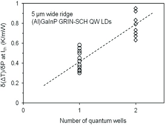
From the viewpoint of obtaining the lowest possible facet heating, lasers with one QW, AlGaAs claddings, and a heat spreader aligned with the mirror edges provide considerable improvements over conventional GaInP laser structures with AlGaInP cladding layers. Thus, the ramped COMD power level could be improved by a factor of 6× (cf. Figure 4.7).
References
Adachi, S. (1983). J. Appl. Phys., 54, 1844.
As, D. J., Epperlein, P. W., and Mooney, P. M. (1987). Inst. Phys. Conf. Ser., 31, 561.
As, D. J., Epperlein, P. W., and Mooney, P. M. (1988). J. Appl. Phys., 64, 2408.
Aspnes, D. E., Kelso, S. M., Logan, R. A., and Bhat, R. (1986). J. Appl. Phys., 60, 754.
Balkanski, M. (ed.) (1971). Light Scattering in Solids, Flammarion, Paris.
Bastard, G. (1981). Phys. Rev., B24, 4714.
Bayramov, B. H., Toporov, V. V., Ubaydullaev, S. B., Hildisch, L., and Jahne, E. (1981). Solid State Commun., 37, 963.
Bhattacharya, P. K., Subramanian, S., and Ludowise, M. J. (1984). J. Appl. Phys., 55, 3664.
Brugger, H. (1990). Nato Advanced Research Workshop on Light Scattering in Semiconductor Structures and Superlattices, Mont Tremblant, Canada.
Brugger, H. and Epperlein, P. W. (1990). Appl. Phys. Lett., 56, 1049.
Brugger, H., Epperlein, P. W., Beeck, S., and Abstreiter, G. (1990). Inst. Phys. Conf. Ser., 106, 771.
Cardona, M. and Güntherodt, G. (eds.) (1975–91). Light Scattering in Solids I–VI, Topics in Applied Physics 8, 50, 51, 54, 66, 68, Springer-Verlag, Berlin.
Chang, R. K. and Long, M. B. (1983). Optical multichannel detection. Chapter 3 in Light Scattering in Solids II (eds. Cardona, M. and Güntherodt, G.), Topics in Applied Physics 49, 179, Springer-Verlag, Berlin.
Chin, A. K., Caruso, R., Young, M. S., and von Neida, A. R. (1984). Appl. Phys. Lett., 45, 552.
Compaan, A. and Trodahl, H. J. (1984). Phys. Rev., B29, 793.
Debbar, N. and Bhattacharya, P. (1987). J. Appl. Phys., 62, 3845.
Elliott, R. J. (1957). Phys. Rev., 108, 1384.
Epperlein, P. W. (1990). Photoluminescence topography studies in III-V semiconductors. In Defect Control in Semiconductors (ed. Sumino, K.), Proceedings of the International Conference on Science and Technology of Defect Control in Semiconductors, The Yokohama 21st Century Forum, Elsevier Science (North-Holland), Amsterdam, 1, 699.
Epperlein, P. W. and Meier, H. P. (1990). Impurity trapping in nominally undoped GaAs/AlGaAs quantum wells. In Defect Control in Semiconductors (ed. Sumino, K.), Elsevier Science (North-Holland), Amsterdam, 2, 1223.
Epperlein, P. W. (1992). IBM Tech. Disclosure Bull., 35, 496.
Epperlein, P. W. (1993). Jpn. J. Appl. Phys., 32, Part 1, No. 12A, 5514.
Epperlein, P. W. (1996). Proceedings of the Conference on Lasers and Electro-Optics, CLEO'96, OSA Tech. Dig., 9, 108.
Epperlein, P. W. (1997). Proc. SPIE, 3001, 13.
Epperlein, P. W. and Bona, G. L. (1993a). Appl. Phys. Lett., 62, 3074.
Epperlein, P. W. and Bona, G. L. (1993b). Proceedings of the Conference on Lasers and Electro-Optics, CLEO'93, OSA Tech. Dig., 11, 478.
Epperlein, P. W., Fried, A., and Jakubowicz, A. (1990). Chapter 8, in Inst. Phys. Conf. Ser., 112, 567.
Epperlein, P. W., Bona, G. L., and Roentgen, P. (1992). Appl. Phys. Lett., 60, 680.
Epperlein, P. W., Hunziker, G., Daetwyler, K., Deutsch, U., Dietrich, H. P., and Webb, D. J. (1995). Chapter 5 in Inst. Phys. Conf. Ser., 141, 483.
Ferenczi, G., Horvath, P., Toth, F., and Boda, J. (1984). US Patent No. 4437060.
Ferenczi, G., Boda, J., and Pavelka, T. (1986). Phys. Status Solidi (a), 94, K119.
Ghezzi, C., Gombia, E., and Mosca, R. (1991). J. Appl. Phys., 70, 215.
Guidotti, D., Hovel, H. J., Albert, M., and Becker, J. (1987). Room temperature photo-luminescence imaging of dislocations. In Review of Progress in Quantitative Nondestructive Evaluation (eds. Thompson, D. and Chimenti, D.), Plenum Press, New York, 6B, 1369.
Hamilton, B., Singer, K., and Peaker, A. (1985). Inst. Phys. Conf. Ser., 79, 241.
Hovel, H. J. and Guidotti, D. (1985). IEEE Trans. Electron Devices, 32, 2331.
Jakubowicz, A. and Fried, A. (1993). Proceedings of the 182nd Electrochemical Society Meeting, 93-10, 212.
Jordan, A. S., Caruso, R., and von Neida, A. R. (1980). Bell Syst. Tech. J., 59, 593.
Leo, K., Rühle, W., and Hägel, N. (1987). J. Appl. Phys., 62, 3055.
Lang, D. V. (1974). J. Appl. Phys., 45, 3023.
Luciano, M. J. and Kingston, D. L. (1978). Rev. Sci. Instrum., 49, 718.
Masselink, W. T., Klein, M. V., Sun, Y. L., Chang, Y. C., Fischer, R., Drummond, T. J., and Morkoc, H. (1984a). Appl. Phys. Lett., 44, 435.
Masselink, W. T., Chang, Y. C., and Morkoc, H. (1984b). J. Vac. Sci. Technol., B2, 376.
Melngailis, I., Stillman, G. E., Dimmock, J. O., and Wolfe, C. M. (1969). Phys. Rev. Lett., 23, 1111.
Meynadier, M. H., Brum, J. A., Delalande, C., Voos, M., Alexandre, F., and Lievin, J. L. (1985). J. Appl. Phys., 58, 4307.
Miller, R. C., Tsang, W. T., and Munteanu, O. (1982). Appl. Phys. Lett., 41, 374.
Mooney, P. M. (1990). J. Appl. Phys., 67, R1.
Pankove, J. I. (1975). Optical Processes in Semiconductors, Dover, New York.
Phillips, J. C. (1981). J. Vac. Sci. Technol., 19, 545.
Raman, C. V. (1928). Ind. J. Phys., 2, 387; Nature, 121, 619.
SEMILAB Ltd (2012). Products. http://www.semilab.hu.
Uji, T., Suzuki, T., and Kamejima, T. (1980). Appl. Phys. Lett., 36, 655.
Wakefield, B., Leigh, P. A., Lyons, M. H., and Elliott, C. R. (1984). Appl. Phys. Lett., 45, 66.
Yamanaka, K., Naritsuka, S., Mannoh, M., Yuasa, T., Nomura, Y., Mihara, M., and Ishii, M. (1984). J. Vac. Sci. Technol., B2, 229.
Yamanaka, K., Naritsuka, S., Kanamoto, K., Mihara, M., and Ishii, M. (1987). J. Appl. Phys., 61, 5062.
Yokogawa, M., Nishine, S., Matsumoto, K., Akai, S.-I., and Okada, H. (1984). Jpn. J. Appl. Phys., 23, 663.
Yu, P. Y. and Cardona, M. (2001). Fundamentals of Semiconductors, 3rd edn, Springer-Verlag, Berlin.