
Chapter 3
Dopant Diffusion: Modeling and Technological Challenges 1
3.1. Introduction
Semiconductor doping is a key element for manufacturing electronic devices. Indeed, a pure (intrinsic) semiconductor is almost an insulator at room temperature, with a valence band almost entirely full, and a conduction band almost entirely empty. As an example, the intrinsic density of mobile carriers in silicon is only about 1010 cm-3 at 300 K. The interesting electronic properties are obtained thanks to the possibility of “doping” the material by introducing adequate impurities (dopants), making it possible to introduce mobile carriers. In fact, the functioning of all the active electronic devices mainly relies, if not entirely, on the possibility of forming P/N junctions, i.e. to put in contact areas doped with an acceptor (impurity having an electron deficit compared to the matrix, involving a conduction by “holes” in the valence band) and areas doped with a donor (impurity having an electron excess compared to the matrix, involving “free electron” conduction in the conduction band). In silicon and germanium (elements of column IV of the periodic table), donors are elements of column V (the most frequently used being phosphorus and arsenic), while acceptors are elements of column III (the most frequently used being boron).
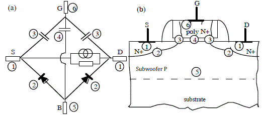
The detail of the electric behavior of a semiconductor device thus strongly depends on the dopant distribution inside the structure. For evidence, we need to compare, for example, the equivalent electric circuit of an N-channel MOS transistor (see Figure 3.1a) with the schematic structure of the same device realized in standard ULSI technology (see Figure 3.1b). As shown in Figure 3.1 (see the numbers indicating the correspondences on the figures), all the elements controlling the functioning of the device (access resistances, conductance and transconductance, capacitances, etc.) are directly associated with the presence of dopants.
Figure 3.1.N-MOS transistor: equivalent electric circuit (a) and corresponding technological structure (b)
Although in modern technologies, dopants are introduced by ion implantation (see Chapter 2 of this book by J.J. Grob), high temperature annealing is necessary, to restore for example the crystalline quality of the material damaged by ion implantation and “to activate” the dopants (i.e. to position them in the substitutional site, where they are electrically active). During these high temperature processes, dopant profiles (i.e. their distribution in the material) are distorted because of the completely general phenomenon of thermal diffusion. Among other things, these diffusion phenomena are particularly critical for the control of the following key parameters:
– Channel doping: the dopant profile in the channel zone, under the gate oxide, determines the importance of the band bending in functions of the various applied voltages. Dopant profiles in this zone thus directly affect the value of the threshold voltage of the device.
– Channel length: the horizontal distance separating the drain from the source. Geometrically defined by photo-lithography steps, the effective length of the finished device is controlled by the dopant lateral diffusion from the drain and source zones.
– Depth of the drain and source junctions: the decrease of lateral dimensions also require us to use increasingly thin junctions, and thus to control as well as possible the penetration of dopant profiles.
– Access resistance: the concentration of electrically active dopants in drain and source zones and their precise distribution also determine the parasitic resistance in series with the transistor channel. This crucial parameter is one of the limiting points for the development of ultimate devices.
With the above examples, we can see that a good control of the electric properties of an electronic semiconductor device requires perfect control of the dopant profiles in the structure, and thus control as precise as possible of the diffusion steps (high temperature annealing) undergone by the circuit throughout its manufacture. This goes by the understanding and modeling of the elementary mechanisms governing the dopant diffusion (the subject of the following development). First, (section 3.2) we will present the general theory of diffusion in solids, applied to the case of semiconductors. Then, (section 3.3) we will take a closer look at the case of dopants in silicon, from experimental (sections 3.3.1 and 3.3.2) and theoretical (modeling, section 3.3.3) points of view. We will describe some practical problems for the device realization (section 3.4). Before concluding, we will briefly approach the case of germanium, a semiconductor which will probably be used in the upcoming technologies (section 3.5).
3.2. Diffusion in solids
3.2.1. General information
3.2.1.1. Fick’s first law
Let us consider an element A dissolved inside a crystalline matrix. At low temperature, the system is frozen and the impurity is immobile. On the other hand, if the temperature is sufficiently raised, under the effect of thermal agitation, the atoms of A are mobile and can move inside the matrix. They are then subjected to the diffusion phenomenon: a non-uniformity of thermodynamic variables (a concentration variation of A, everything otherwise equal, being the most frequent case) induces a transport of matter (a displacement of atoms A) inside the solid. Diffusion is thus a non-reversible process. Its “driving force” is the gradient of chemical potential and it aims to homogenize this potential. The general phenomenological description of this process is only possible with the use of the thermodynamics theory of irreversible processes, which is beyond the subject of this section.
However, in the simplest case of only one diffusing species subjected only to its concentration gradient, the phenomenon is very simply described, using Fick’s first law. This law stipulates that the impurity flux J (number of atoms crossing the surface unit per time unit) is proportional (in absolute value) to the concentration gradient C of the impurity:
[3.1] ![]()
The sign “—” of the equation above simply shows the fact that diffusion occurs from high concentration zones towards low concentrations zones. This is required to be able to homogenize the concentrations.
By definition, the proportionality factor D is the diffusion coefficient, or diffusivity. The flux is generally expressed in atoms per square centimeter and per second (cm-2s-1) and concentrations in the number of atoms per cubic centimeter (cm3). D is then practically expressed in cm2s-1. We can notice the analogy of this law with the heat transfer, Fourrier’s law ![]() or with the elementary electric current Ohms law
or with the elementary electric current Ohms law ![]()
It is important to realize that the flux is a vector quantity and that thus, in the most general case (anisotropic environment), D is a tensor. Therefore, the flux is not necessarily parallel to the concentration gradient. This can occur in non-cubic or distorted materials, under a stress for example. Nevertheless, the case interesting to us here is silicon, a cubic material and thus isotropic in the absence of strain. In the silicon case, the diffusion coefficient is a scalar. The flux, given by the first Fick equation is then parallel to the concentration gradient.
Therefore, we will be able to consider in the following, without losing the sense of general information, only the 1D case for which Fick’s first law is reduced to:
[3.2] ![]()
3.2.1.2. Generalized flow: drift terms
Previously, we have considered that the diffusing impurity was only subjected to its concentration gradient. Let us consider now the most general case, where the impurity is submitted to driving forces of various origins (concentration gradient, stress field, electric field, etc.) and which, under the effect of these forces (and of its inevitable interactions with the crystal lattice) acquires an average stationary speed <v>. It is then easy to show that the impurity flux is given by the equation:
[3.3] ![]()
The general problem thus reduces to identifying the nature of the various forces and to establishing the relation between force and speed. On the assumption that the driving force is only due to the concentration gradient, the thermodynamics of the irreversible processes shows that the driving force is the gradient of the partial mixing entropy. The calculations then lead to equation [3.2]. In the general case of a set of driving forces, while intuitively admitting that the average speed of the impurity is the sum of the elementary speeds induced by each driving force taken separately, it is convenient to write the impurity flux as:
[3.4] ![]()
In the previous equation, the first term (“Fickian” term) shows the contribution of the lone concentration gradient and the second term (“Nernstian” or “drift” term) is the contribution of all the other driving forces. An important case is that of a charged species in the presence of an electric field. Under these conditions, the drift velocity is given by:
[3.5] ![]()
where µ is the mobility, E is the electric field and the sign ± is dependent on the sign of the charge carried by the impurity. Under these conditions, the flux is simply written:
[3.6] ![]()
As we will see further, this expression of the flux, well-known in electric charge transport theory, also has its utility for the problem of dopant diffusion in a semiconductor.
3.2.1.3. Fick’s second law and simple profiles calculation
Established for a conservative system, i.e. where there is neither loss nor creation of diffusing atoms, Fick’s second law describes the temporal evolution of the concentration of the diffusing species at a given point. A simple mass balance leads to the following conservation equation (or continuity equation):
[3.7] ![]()
From where we take:
[3.8] ![]()
If D can be regarded as constant, i.e. independent of the concentration, and thus independent of x and t, in the hypothesis of a diffusion under the only effect of a concentration gradient, equation [3.2] gives:
[3.9] ![]()
For a species submitted to additional driving forces, equation [3.4] with constant D leads to:
[3.10] ![]()
When the system is not conservative, for example in the event of chemical reaction inducing the formation or the elimination of impurities, or of the trapping of impurities, etc., these equations are modified by the addition of generation or recombination terms, which depend on the mechanisms involved. We will see further an essential example to describe some non-equilibrium situations.
Equation [3.9] (Fick’s second equation) is thus only valid for very restrictive conditions which, as we will see later on, are seldom met for the diffusion problems in semiconductors. Equations [3.9] or [3.10] are the basis for the calculation of C(x, t), but regarding partial differential equations, of the first order in t and of the second order in x, their solutions are not unique. The appropriate solution for a given situation is determined by the knowledge of an initial condition and of two limit conditions describing the experimental reality. In general, the solution of these equations is not analytically possible. It is thus necessary to resort to numerical resolutions by computer.
Nevertheless, Equation [3.9] has simple analytical solutions for particular initial and limit conditions. These conditions are generally imposed from an experimental point of view, in order to be able to determine the values of diffusion coefficients by comparison between the measured profiles and these simple laws. We will give here these solutions for three practical cases. The reader can refer to the reference books by Carslaw and Jaeger [CAR 59] or Cranck [CRA 75] for a more comprehensive catalogue and for the demonstration of the results below:
– Diffusion from a thin layer: this is the practical case, where the diffusing species is deposited at the initial moment, in the form of a thin film on the surface (x=0) of a very thick sample. If there is no impurity evaporation, as soon as the penetration depth is very large compared to the initial film thickness, the concentration profile follows a Gaussian law inside the sample:
[3.11] ![]()
where Q is the total quantity of the deposited impurity (and thus dissolved in the material):
[3.12] ![]()
– Diffusion with a constant surface concentration: this is the case where an infinite external source maintains on the surface of the sample a constant concentration C0. The solution then calls upon a conventional function of the statistics, the complementary error function:
[3.13] ![]()
with:
Figure 3.2. Complementary error function
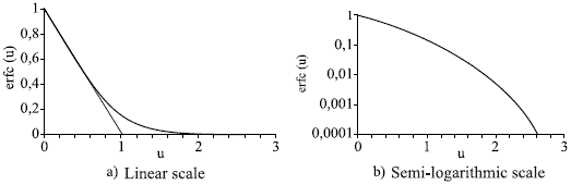
Existing numerical tables give the values of the complementary error function. Its variation according to ![]() is given in Figure 3.2, in linear and semi-logarithmic scale. As we can see in Figure 3.2a, the tangent at the origin cuts the abscissa-axis at the point u=1, i.e.
is given in Figure 3.2, in linear and semi-logarithmic scale. As we can see in Figure 3.2a, the tangent at the origin cuts the abscissa-axis at the point u=1, i.e. ![]() The impurities dose ranging between this point and the sample surface approximately represents 90% of the total dose penetrated in the sample
The impurities dose ranging between this point and the sample surface approximately represents 90% of the total dose penetrated in the sample ![]() We can thus consider, with a good approximation that the depth affected by the diffusion is about
We can thus consider, with a good approximation that the depth affected by the diffusion is about ![]() which explains why this quantity is often called the diffusion depth.
which explains why this quantity is often called the diffusion depth.
- Redistribution of a buried Gaussian: this is the simplest approximation of the redistribution of a dopant profile introduced by ion implantation. As a first approximation, the corresponding initial profile is Gaussian:
[3.15] ![]()
Rp is the mean projected range and ∆Rp is the standard deviation. If Rp is sufficiently large so that the impurity profile does not interact to a significant degree with the surface during the diffusion, and if the diffusivity can be considered constant, the profile obtained at the end of a time t is always a Gaussian centered in x=Rp, therefore given by a relation similar to equation [3.15]. Its maximal value and standard deviation vary with time, according to the following laws:
[3.16] ![]()
and:
[3.17] ![]()
3.2.1.4. Boltzmann-Matano analysis
When D depends on the concentration or more generally varies with the coordinates of space or time, equations [3.9] or [3.10] are no longer valid, and the general continuity equation [3.8] cannot be integrated any more simply.
However, an estimate of the variation of the diffusivity with C can be obtained from the experimental diffusion profile by the Boltzmann-Matano method: by the change of variable ![]() the partial differential equation [3.8] is easily transformed into a simple differential equation:
the partial differential equation [3.8] is easily transformed into a simple differential equation:
[3.18] ![]()
If the boundary conditions are simply expressed according to the only variable λ (which is the case for example for a diffusion with constant surface concentration, but not for the redistribution of a thin film or a Gaussian), a double integration leads to the following relation:
[3.19] 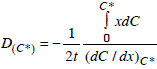
As seen in Figure 3.3, the numerator of this expression is the area ranging between the profile C(x, t), the axis x and the line C=C*, whereas the denominator is the tangent to the profile at the point C=C*.
This geometrical interpretation of relation [3.19] makes the determination of D possible by graphic means from the experimental profile.
Figure 3.3. Boltzmann-Matano analysis
3.2.2. Elementary mechanisms
3.2.2.1. Atomic mechanisms
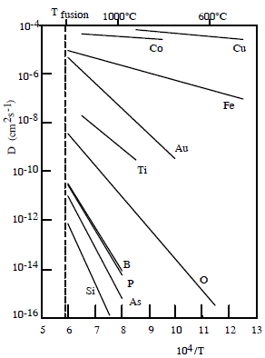
Figure 3.4 sums up the variation with the temperature of the diffusivity of various impurities experimentally measured in intrinsic silicon. We note that, depending on the type of impurity, the experimental values have very different orders of magnitude, ranging, for a temperature of about 900°C, from 10-5/10-4 cm2s-1 for impurities such as copper or cobalt, up to values of about 10-16/10-15 cm2s-1 for the common dopants (P, B, As). Correlatively, the activation energies (see section 3.2.2.2) involved vary from 0.2/0.5 eV to 4 or 5 eV. This variety of orders of magnitude of the diffusion coefficient simply reflects the different microscopic mechanisms by which an impurity atom can move in a crystalline solid. These mechanisms are closely related to the atomic structure (network) of the concerned solid and to the equilibrium position of the impurity in the crystal lattice of the matrix.
Figure 3.4. Diffusivities in intrinsic Si
According to this equilibrium position (stable site), we distinguish substitutional impurities, whose stable site is a crystal lattice site of the matrix, and interstitial impurities, whose stable site is between the network sites (in a void between the matrix atoms).
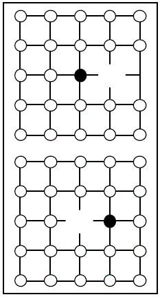
Interstitial impurities: this is the simplest mechanism, illustrated in Figure 3.5, during which the impurity gradually “hops” from interstitial site to interstitial site and can thus easily cover significant distances. This mechanism thus leads to high diffusion coefficient. In silicon, light elements (H, He, etc.) and transition metals of the 4th line of the periodic table (Ti, V, Cr, etc.) behave according to this pattern. Although it does not directly concern this chapter, essentially devoted to the dopant behavior, we will nonetheless point out that direct interstitial diffusion is often slowed down by the interactions of the diffusing species with the other present impurities (in particular the dopants), leading to the formation of more or less stable complexes and to an important reduction of the effective diffusion coefficient. The interested reader will be able to refer, for example, to the references [MAT 89] and [HEI 99], respectively discussing the case of hydrogen and copper. In the case of transition metals, these interactions must necessarily be taken into account for a good understanding of the technological steps, aiming at trapping these impurities (gettering).
Figure 3.5. Simple interstitial diffusion

Substitutional impurities: the diffusion of these impurities is only possible by involving the structural point defects of silicon. These defects are either vacancies (vacant sites in the network), or self-interstitial (surplus silicon atoms in the network), which gives place to two types of elementary diffusion mechanisms:
– The vacancy mechanism is illustrated in Figure 3.6: to diffuse, the impurity must wait until a vacancy reaches its neighborhood. The diffusion is then carried out by sites exchange between the impurity and the vacancy. In the most general case, this vacancy can then move away from the impurity atom, by exchanges with the neighboring silicon atoms, and the impurity atom must expect the arrival of another vacancy to perform an additional hop. On the other hand, because of a strong binding energy between the vacancy and the impurity, the considered vacancy can happen to remain in close proximity with the impurity and the corresponding complex can diffuse as such in the network. Later on we will reconsider this diffusion concept with “pairs”.
Figure 3.6. Vacancy diffusion
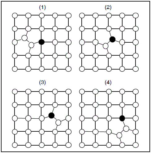
– Figure 3.7 shows the diffusion mechanism assisted by self-interstitials. In the silicon network, self-interstitials have the structure schematized in (1): the interstitial remains linked to the network and is in fact a “dissociate self-interstitial”, i.e. two silicon atoms share a single network site. When this self-interstitial is in the proximity of a substitutional impurity, one of the silicon atoms can interact with the impurity, which leads to the formation of an interstitial impurity (schematized in (2)). This is in fact a “mixed dissociate interstitial”, then able to diffuse according to the hopping sequence described in Figure 3.7. In the example illustrated here, the mixed interstitial is dissociated (with reforming of the self-interstitial) after a hop of the impurity. In fact, in the effective 3D silicon network, the mixed interstitial (the interstitial impurity) can carry out several hops and thus diffuse on long distances, before dissociating. All occurs then as if it was the diffusion of an impurity/self-interstitial “pair”.
Figure 3.7. Diffusion assisted by self-interstitials
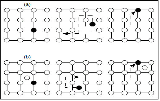
Dissociative mechanisms: these mechanisms occur for impurities, the stable site of which is a substitutional site (where they are relatively immobile). But these impurities have a noticeable probability of existence in an interstitial site (with a very high diffusion coefficient). The resulting effective diffusivity, with values intermediate between those of the substitutional and pure interstitial impurities, is mainly governed by the mechanism allowing the considered impurity to go from one type of site to another. According to the type of point defect implied in these exchanges (see Figure 3.8), we distinguish two dissociative mechanisms:
– The “Frank-Turnbull” mechanism: schematized in Figure 3.8a, this mechanism was initially proposed to explain the copper diffusion in germanium [FRA 56]. It involves the substitutional impurity/interstitial impurity exchange via network vacancies, according to the reaction:
[3.20] ![]()
– The “kick-out” mechanism: the previous mechanism was regarded for a long time as suitable to describe the diffusion of the “heavy” transition metals (Pt, Au, etc.) in silicon. However, it was then shown that it was not convenient for a proper description of all the experimental observations. A new mechanism, involving self-interstitials, known as “kick-out”, was proposed by Gösele [GOS 80]. In this mechanism, illustrated in Figure 3.8b, a self-interstitial can eject a substitutional impurity of its site, leading to the formation of an interstitial impurity. The opposite reaction would lead to the return of the impurity into the substitutional site:
[3.21] ![]()
In the previous equations, A indicates the impurity (the index informing about its site), V designates a vacancy and I, a self-interstitial. Without going into the details, let us say that only a combination of the two previous mechanisms is suitable for a comprehensive description of the diffusion profiles of gold in silicon [MAT 92].
It is moreover interesting to notice that the diffusion mechanism of the substitutional impurities assisted by self-interstitials is identical to the kick-out mechanism, if the hypothesis is made that the interstitial impurity remains linked to the network. In fact, these two mechanisms, introduced and described in different contexts, lead to the same continuity equations and it is in general not easy (nor often even relevant) to distinguish them.
Figure3.8. Dissociative mechanisms: (a) “Frank-Turnbull”; (b) “kick-out”
3.2.2.2. Atomic theory of the diffusion coefficient
As seen in Figure 3.4, the experimental variations of the diffusion coefficients with the temperature can in general be easily described by an Arrhenius law:
[3.22] ![]()
T is the absolute temperature (in Kelvin) and k is the Boltzmann constant. The parameter Q is called the diffusion activation energy. If we consider that during its displacement, the diffusing species jump from one stable site to another with a frequency v, this energy Q is also the activation energy of v:
[3.23] ![]()
This activation energy concept is easily illustrated using Figure 3.9, which schematically describes the fluctuation of Gibbs free enthalpy (G) of the crystal during the displacement of the diffusing species. When the diffusing species is on its stable site (S), G is minimal (situation of thermodynamic equilibrium). Because of the thermal agitation, the atom vibrates with a frequency v0 close to the Debye frequency of the crystal (about 1013 s-1). This displacement must be accompanied by a lattice deformation, and thus by an increase of G. In a certain point, called the saddle point (C), halfway between two stable sites, G passes by a maximum. If, thanks to thermal agitation, the diffusing species reaches this saddle point, it can then “fall” into the other stable site, without additional energy cost. The activation energy is thus the difference in Gibbs free enthalpy of the crystal between its value at the saddle point and the equilibrium value.
Figure3.9. Activation energy concept

For a given atomic mechanism, the activation energy, as well as the pre-exponential term D0, can be connected to the physical parameters describing the elementary hop. First of all, it is necessary, independently of the mechanism involved, to establish the relation between the diffusivity and the jump frequency. It is obvious that, whatever the elementary mechanism, an atom can move in a crystal only by a series of elementary hops. If these hops take place in a completely random way (each hop being independent of the previous hop), we speak about a “random walk”. We can then show (for example [PHI 91], [TUC 74]) that, in a cubic crystal, the diffusion coefficient is connected to the jump frequency by the relation:
[3.24] ![]()
where a is the length of the elementary hop, i.e. the distance between the first neighboring atoms (a= 2.35 Å for silicon). In reality, atomic hops do not occur purely randomly. Indeed, a hop could be correlated to the previous hop. This results in the introduction of a corrective multiplicative factor f into equation [3.24]. This correlation factor is lower than unity, and its value depends on the crystal lattice structure and on the atomic diffusion mechanism. We can now understand the microscopic origin of the orders of magnitude of the activation energies for various diffusion mechanisms.
Substitutional impurity: for the vacancy mechanism or for the mechanism assisted by self-interstitials, two conditions must be filled to allow an atomic hop of the impurity to happen. First, it is necessary that the defect is in the immediate proximity (first neighbor) of the impurity, which is characterized by a probability Px. It is then necessary that the defect exchange its site with the impurity, which occurs with a frequency vX. The hopping frequency of the impurity is thus the product of these two terms:
[3.25] ![]()
with, according to the already explained approach (see Figure 3.9):
[3.26] ![]()
![]() is the migration free enthalpy of the defect X, which is naturally broken down (G=H-TS) into a migration entropy
is the migration free enthalpy of the defect X, which is naturally broken down (G=H-TS) into a migration entropy ![]() and a migration enthalpy
and a migration enthalpy ![]() If we assume the defects are distributed in a purely statistical way in the crystal, the probability of having a defect X in the proximity of the impurity is simply the proportion of crystal sites occupied by a defect X. However, for most impurities, there is a binding energy
If we assume the defects are distributed in a purely statistical way in the crystal, the probability of having a defect X in the proximity of the impurity is simply the proportion of crystal sites occupied by a defect X. However, for most impurities, there is a binding energy ![]() between the impurity and the defects, so that the probability Px is given by:
between the impurity and the defects, so that the probability Px is given by:
[3.27] ![]()
where CX is the volume atomic concentration of defect X at temperature T, and NS the volume density of network sites (5×1022 cm-3 for silicon). Simple thermodynamic considerations enable us to show that, at a temperature T different from the absolute zero (0 K), any crystal contains a non-null equilibrium concentration of defects, given by:
[3.28] ![]()
where ![]() is the free enthalpy of formation of the defect X,
is the free enthalpy of formation of the defect X, ![]() and
and![]() being the corresponding entropy and enthalpy.
being the corresponding entropy and enthalpy.
By combining the previous various relations, we then easily show that the diffusion coeficient is well described by relation [3.22] with:
[3.29] ![]()
and:
[3.30] ![]()
By introducing the diffusion coefficient of the defect (DX = (1/6)a2vX ), we easily obtain the diffusivity of the substitutional impurity according to the macroscopic parameters of the defect:
[3.31] ![]()
This proves that the diffusion coefficient of a substitutional impurity is directly proportional to the concentration of the point defect, which it uses as a “vehicle”. This basic concept is at the base of a rigorous interpretation of the diffusion “anomalies”, which we will see later on.
Interstitial impurity: in this case, the analysis is much simpler. Indeed, the point defects are not involved here and, as long as its concentration remains low (which is generally the case for impurities in silicon), the impurity has a probability equal to 1 to find a vacant interstitial site within its proximity. We then simply obtain:
[3.32] ![]()
and:
[3.33] ![]()
![]() and
and ![]() being the migration entropy and enthalpy of the interstitial impurity.
being the migration entropy and enthalpy of the interstitial impurity.
3.2.3. Semiconductor specificities
The previous sections describe the diffusion of an impurity in a crystalline solid, independently of the type of solid considered. In this section, we discuss the specificities to be taken into account in the case of diffusion in semiconductors. These additional effects are essentially related to the modulation of the position of the Fermi level in the band gap, under the doping influence.
3.2.3.1. Doping influence
It was very quickly observed in experiments that the value of the diffusion coefficient in semiconductors is affected by the doping level of the material. A typical and perfectly interpreted example is the influence of a high dopant concentration on the self-diffusion coefficient of germanium [VAL 57]. In this particular case, an N doping increases the diffusivity, whereas a P doping decreases it. This phenomenon is easily explained by considering the specificity of the semiconductor state, regarding the structure of point defects. The semiconductor state is characterized by the existence of a forbidden band (the “gap”), i.e. an energy domain where the electronic states density is null. But this perfect forbidden band structure is closely related to the crystal lattice periodicity. Thus, any local break of this periodicity (induced for example by the presence of an impurity or a point defect) can induce a possible electronic state inside the gap, spatially restricted to the immediate proximity of the defect. We then say that the defect introduces a “deep level”. The occupation of this level by an electron is obviously governed by the Fermi-Dirac statistics and thus depends on the position of the Fermi level in the gap (itself controlled by doping). For example, we know that the vacancy in germanium introduces an acceptor level into the gap, so that the vacancy can be neutral (V0) or negatively charged (V-), depending on whether the level is empty or occupied. From Fermi-Dirac statistics, we easily obtain the relative concentrations of these states of charge, according to doping:
[3.34] ![]()
with:
[3.35] ![]()
In the previous equations, EA is the position of the deep level introduced by the vacancy, EF is the Fermi level, and n is the density of free electrons in the conduction band. The index i indicates the intrinsic values. The total vacancy concentration is thus given by:
[3.36] ![]()
As the thermal equilibrium imposes the concentration value of neutral vacancies, it results from the previous relation, that the total vacancies concentration strongly depends on the doping level. The defects are used as diffusion “vehicle”, whatever their state of charge. Therefore, the diffusion coefficient depends on the doping level.
We can now easily interpret the results concerning the germanium self-diffusion: a strong doping with donors increases the value of n, and thus the total vacancy concentration, while a doping with acceptors decreases n, inducing a decrease of the total vacancies concentration. This is in perfect agreement with the experimentally observed fluctuations [VAL 57].
In the case of silicon, the situation is slightly different. Indeed, the silicon point defects (vacancies or self-interstitials) have an amphoteric behavior: they introduce deep acceptor and donor levels, so that the total defect concentration is increased by the two doping types, donor or acceptor. Later on we will see that these effects must be accounted for to explain the diffusion profiles of the silicon dopants.
3.2.3.2. Influence of the induced electric field
Another important effect must imperatively be taken into account in the semiconductors, in the presence of a dopant gradient. Let us consider for example a non-polarized silicon sample containing phosphorus (donor element) in variable concentration. This concentration gradient of donors necessarily implies the existence of a concentration gradient of free electrons. In order to maintain the equilibrium (absence of electric current), the electron flux, induced by this concentration gradient is balanced by the establishment of a space charge built-in electric field, given by the conventional formula:
[3.37] ![]()
Let us now consider the dopant flux. At high temperature (necessary condition so that the dopant is mobile), the donor atoms are entirely ionized, so that phosphorus is a positively charged ion (P+). In the presence of an electric field, it is thus necessary to use the generalized form of the flux, given by equation [3.6]. By using equation [3.37], we then obtain:
[3.38] 
where the Einstein relation (D/µ = kT/q) is used to express the mobility as a function of D. In addition, in the absence of external polarization, the free electrons concentration is locally connected to the phosphorus concentration by the equation of electrical neutrality:
[3.39] ![]()
Thus, the gradient of n can be expressed according to the gradient of [P+], and it is then possible to put the flux equation in the form of Fick’s first law, with an effective diffusivity depending on local doping:
[3.40] ![]()
with:
[3.41] ![]()
The corrective term h is the acceleration factor related to the electric field induced by the dopant gradient, and its value varies from 1 at low doping (n = ni) to 2 at the most at very high doping (n >> ni).
In the case of an acceptor gradient (for example boron in Si), we obtain a completely similar relation, by replacing the free electrons concentration with the holes concentration (p):
[3.42] ![]()
Lastly, the two effects described above (influence of doping and built-in electric field) are sensitive only for dopant concentrations higher than the density of intrinsic carriers at the diffusion temperature (about several 1018 to 1019 cm-3 towards 800 – 1,100°C in Si). For lower concentrations, the concentration of the free carriers remains equal to the density of intrinsic carriers and the corrective terms are equal to 1.
3.3. Dopant diffusion in single-crystal silicon
3.3.1. Predeposition methods
The predeposition term designates a technological step during which a controlled quantity of dopant is locally introduced into the substrate. This generally is a dopant of the type opposite to the substrate dopant. This leads to the realization of various P/N junctions, necessary to the device architecture. These steps, crucial for the optimization of the device electrical characteristics, require a reproducibility and a perfect control of the introduced dopant doses, and of their spatial distribution. That is essentially why, over several decades, ion implantation has become the standard technique to carry out predeposition of dopants in microelectronics. This specific technique is the subject of a complete chapter in this book and will not be discussed here.
Nevertheless, some specific devices, such as photovoltaic cells for example, do not support an ion implantation step, which would deteriorate the life time of minority carriers too much and which is also more expensive. For this type of devices, we continue to use the same techniques as those initially used in microelectronics, namely diffused predepositions. We distinguish two types of predepositions, according to whether the dopant transportation towards the silicon wafer occurs in vapor phase or simply in solid phase.
3.3.1.1. Predepositionin vapor phase
The principle of the predeposition technique in vapor phase, schematized in Figure 3.10, is relatively simple to implement. It simultaneously treats a batch of several wafers, which is an unquestionable economical interest. The wafers to be doped are put inside a diffusion furnace, made up of a quartz tube surrounded by heating elements, in which we maintain a certain partial pressure of the doping gas. Let us note that a neutral carrying gas (nitrogen) permanently circulates in the tube, in order to avoid any pollution by elements coming from the surrounding air. This nitrogen must be very pure, in order not to pollute the furnace. To decrease even more contamination risks, diffusion tubes with double inner walls are often used. An ultrapure gas flow (in general nitrogen) circulates between those inner walls.
The simplest dopant sources to implement are gases such as arsine (AsH3) or phosphine (PH3) for N doping (with donors), or diborane (B2H6) for P doping (with acceptors). However, these gases are dangerous or even lethal at very low concentration. In general, we thus prefer using liquid sources, such as POCl3 or BBr3. They are liquid at room temperature, but easily vaporized to be introduced into the diffusion furnace.
Figure3.10. Schematic representation of a diffusion furnace for predepositionin the gaseous phase
We can also use solid sources, such as certain glasses, containing dopants, like boron nitride or a glass doped with phosphorus. These sources are in the form of slices and are in general introduced into the furnace, alternately with the wafers to be doped. During the high temperature thermal process, the dopant contained in these source materials evaporates and thus maintains a partial pressure of dopants in the proximity of the silicon wafers.
Whatever the type of source used, during the high temperature predeposition step, part of the doping atoms, transported by the gaseous phase, enters from the surface in the silicon volume. After the sources withdrawal, once the desired total dose is reached, the doping elements are further diffused towards the bulk of the substrate, by an additional thermal step (at high temperature) to obtain the desired profile.
3.3.1.2. Deposition in the solid phase
In this technique, the dopant source, consisting of a thin film of a material containing the adequate impurity, is directly deposited on the surface of the silicon wafer.
The most convenient is to use “doping pastes” in the form of sol-gel solutions of strongly doped glasses (borosilicates, phosphosilicates), easily deposited by spin-coating, with the same principle as the deposition of photosensitive resists for lithography.
After stoving to evaporate the solvent, the wafers covered with doped glass are introduced into a diffusion furnace to undergo the high temperature thermal treatment, inducing the dopant diffusion from the film deposited towards the bulk of silicon. The use of this type of source also allows us to use rapid thermal annealing techniques, similar to those used to activate the dopants after the ion implantation step.
3.3.2. Main experimental observations
3.3.2.1. Diffused predepositions in neutral atmosphere
One of the striking facts concerning dopant diffusion in silicon is the tremendous influence of the dopant concentration on the shape of the diffusion profiles. This influence is easily highlighted on the experimental profiles corresponding to diffused predepositions. Let us recall that this technique was used for a long time to introduce dopants into silicon. Although now completely given up in favor of ion implantation (at least for ULSI microelectronic technologies), the corresponding results established the majority of our knowledge on fundamental mechanisms governing dopant diffusion.
This is why we recall these results here. Since the diffused predeposition step corresponds to diffusion with a constant surface concentration, Fick’s laws indicate that the concentration profile should simply be a complementary error function, if the diffusivity is a constant.
In reality, the experimental results are much more complex.
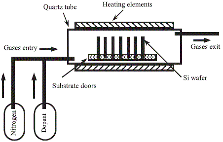
Phosphorus: for example Figure 3.11a shows the various profiles obtained after a one hour predeposition at 1,000°C for various surface concentrations [WIL 77]. For surface concentrations lower than the density of intrinsic carriers, the profile is in accordance with the one expected for a simple diffusion mechanism (complementary error function). On the other hand, when the surface concentration increases, strong nonlinearities are highlighted. Firstly, (surface concentrations of several 1019 cm-3) there is a local increase in the diffusion coefficient at high concentrations, leading to “rectangular” profiles in semi-logarithmic scale. Then, gradually, a slight inflexion appears on the profiles, with a zone with a strong gradient on the surface, followed by a curve “tail” corresponding to a large increase in the effective diffusion coefficient. When the surface concentration exceeds 2 to 3 x 1020 cm-3, an additional phenomenon appears: a concentration plateau, corresponding to a very fast diffusion, visible in the surface zone, is followed by the high gradient zone and the curve tail, as previously. The variation of the effective diffusion coefficient, according to the local phosphorus concentration, obtained by the Boltzmann-Matano method, is shown in Figure 3.11b, for these highest surface concentrations. This figure highlights the strong enhancement of the diffusion in the bulk compared to the diffusivity extracted from conditions at low surface concentrations (intrinsic diffusion), as well as the strong acceleration in the surface region. These two extremes are separated by a zone, where we observe a local decrease in the diffusivity, corresponding to the inflexion area on the experimental profile.
Figure3.11. a) Profiles of phosphorus predeposition at 1000°C. b) Boltzmann-Matano analysis for very high surface concentrations
Arsenic: as in the case of phosphorus, arsenic predeposition profiles at low surface concentrations have a form correctly described by a simple complementary error function, allowing us to extract the intrinsic diffusivity of the impurity. However, when the surface concentration exceeds the intrinsic carriers density, we observe deviations compared to the ideal curve, different from those observed with phosphorus. Indeed, diffusions at temperatures of about 1,000°C lead to profiles of nearly rectangular shape (in semi-logarithmic scale), such as Figure 3.12a (according to [FAI 73]).
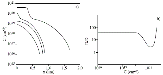
Moreover, as we can notice in the figure, there is a significant difference between the total arsenic concentration and the electrically active concentration, measured by spreading resistance. The result of the Boltzmann-Matano analysis of this experimental profile is given in Figure 3.12b, and shows a clear decrease of the effective diffusion coefficient at high arsenic concentrations, preceded by a domain where the diffusivity is sensibly proportional to the local arsenic concentration, the effective diffusion coefficient tending to its intrinsic value at lower arsenic concentrations.
Figure 3.12. a) Typical profile of arsenic predeposition at high concentration (1,000°C, 1 hr) and b) corresponding Boltzmann-Matano analysis
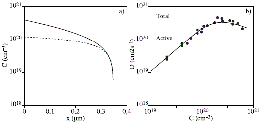
Boron: as for the other dopants, boron predeposition profiles are in conformity with the complementary error function for the intrinsic conditions, whereas nonlinearities exist at higher concentrations. In the case of boron, these nonlinearities appear with sensibly rectangular profiles, such as those of Figure 3.13a (according to [QUO 72]). The corresponding Boltzmann-Matano analysis (see Figure 3.13b) reveals a slight increase of the diffusion coefficient in the bulk, compared to the intrinsic values, and a variation sensibly proportional to the boron concentration at higher concentrations.
Figure 3.13. (a) Typical profile of boron predeposition at high surface concentration at 1000°C and (b) corresponding Boltzmann-Matano analysis for the 60 min profile
3.3.2.2. Couplings between impurities
Interesting pieces of information concerning the mechanisms involved during the dopant diffusion, are obtained when we observe the coupling effects between impurities. As an example, we will consider the processes sequence necessary to manufacture a bipolar “planar” N-P-N transistor. An initial localized diffusion of the acceptor (boron for example) is carried out in an N-type substrate, to form the basis of the transistor. The emitter is then formed by localized diffusion, through a smaller window, of a donor (phosphorus or arsenic) in high concentration. During the second step, there is of course a simultaneous diffusion of the donor and the acceptor. The interactions taking place during these sequential diffusions can separate into two distinct effects, however occurring at the same time.
The first of these effects is caused by the electric field, induced by the donor diffusion, in accordance with what is explained in section 3.2.3.2, and results in the appearance of a dip in the boron profile close to the junction, as illustrated in Figure 3.14 (according to [BLA 72]). To understand the formation of this dip, it is sufficient to realize that the electric field induced by the arsenic gradient is positively directed, and it thus induces a negative contribution to the total flux of the boron atoms, which are negatively charged (see equation [3.6]). The effect can be sufficiently strong to efficiently drift the boron atoms towards the surface. On the other hand, beyond the junction, the concentrations are relatively low, so that the carrier concentration has its intrinsic value and there is no more induced field. Boron atoms thus diffuse exclusively under the effect of their gradient, therefore towards the bulk. These opposite effects in surface and bulk necessarily induce a depletion in boron concentration close to the junction.
Figure 3.14. Coupled boron-arsenic diffusion
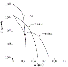
The second effect, illustrated in Figure 3.15a, is known as the “emitter push effect” and is essentially observable for N-P-N structures with phosphorus emitters: the high concentration phosphorus diffusion used for the fabrication of the emitter is accompanied by a more important penetration of the base-collector junction in the zones undergoing phosphorus diffusion at the surface. It is now established (see for example [WIL 77]) that this pushing effect has the same physical origin as the appearance of the tails in the phosphorus profiles. These effects are associated with a local increase of the impurity diffusivities, due to a strong supersaturation of point defects, related to P diffusion. This interpretation in terms of point defects is comforted by the studies of redistribution enhancement of a buried boron layer, caused by a high concentration P diffusion at the surface (see Figure 3.15b).
Figure 3.15. Influence of a localized phosphorus diffusion on boron redistribution: (a) emitter push effect; (b) buried layer extension

This type of experiment makes it evident that acceleration occurs on long distances (several tens of microns), without any direct interaction between the boron layer and the surface phosphorus, and that the order of magnitude of this acceleration is the same as the one observed in the tails of the P profile. It is thus now perfectly accepted that phosphorus diffusion in Si, at high concentration, generates non-equilibrium point defects. Since effects of a similar nature, although of lower intensity, are observed with arsenic emitters, or in boron for P-N-P transistors, it is now considered that the mechanism inducing these defect supersaturations is general for all the common dopants.
3.3.2.3. The oxidation influence
Dopant diffusion in silicon is strongly affected by the atmosphere in which annealing is carried out. In particular, an oxidizing annealing generally involves a diffusion acceleration (OED, oxidation enhanced diffusion) of the common dopants (B, P, As) and a slowing down (ORD, oxidation retarded diffusion) of the antimony. A retarded diffusion is also observed for phosphorus, arsenic and boron under some experimental conditions: Si (111) oxidation at very high temperature during very long times [HIL 81]. The main results are as follows:
– for each dopant, the effect depends on the substrate direction, OED being stronger for the faces (111) than (100);
– OED is more important for oxidation in a wet atmosphere than for a dry oxygen atmosphere, directly related to the oxidation rate increase;
– the addition of chlorinated compounds diminishes OED;
– the relative importance of OED increases when the temperature decreases;
– finally, OED (or ORD) is a long range effect, associated with a supersaturation (or undersaturation) of point defects.
In fact, Hu [HU 74] highlighted that all these pieces of information are in perfect correlation with those concerning the stacking faults behavior (growth or decrease) induced by oxidation. We can thus deduce that the two phenomena are related to the same disturbances on point defects. As we know, thanks to electron microscopy, stacking faults induced by oxidation are of “extrinsic” nature (due to a self-interstitials excess). Therefore, oxidation injects self-interstitials in silicon and the diffusion of boron, phosphorus and arsenic is assisted, at least partially, by self-interstitials (mechanism schematized in Figure 3.7). Moreover, due to the recombination between the defects, a self-interstitial supersaturation necessarily induces a vacancy undersaturation. This explains the antimony diffusion retardation. Indeed, its diffusion, because of its size, is almost exclusively vacancy-assisted. However, as the diffusion of the other dopants can also be retarded by oxidation, it is now accepted that dopant diffusion is assisted by the two types of point defects, vacancies and self-interstitials. The appearance of OED or ORD simply depends on the relative importance of each mechanism for the considered dopant and of the self-interstitial supersaturation level (or the vacancy undersaturation level) peculiar to each experimental condition.
3.3.3. Modeling
3.3.3.1. “Normal” diffusion
As long as the experimental characteristics observed on the diffusion profiles do not involved non-equilibrium defects, it is possible to simply model the dopant diffusion, using the mechanisms described above. In particular, profiles with concentrations lower than the intrinsic carriers density are perfectly described thanks to Fick’s second law, with a constant diffusion coefficient. This coefficient is called the intrinsic diffusivity and is usually noted Di. The variation of these intrinsic coefficients with the temperature is shown in Figure 3.4, and the corresponding values of activation energies and of the pre-exponential terms are given in Table 3.1 for common dopants. These values represent the average of various experimental sources ([MAT 84] and included references).
Table 3.1. Intrinsic diffusion in Si
| Dopant | D0 (cm2s-1) | Q (eV) |
| P | 3.19 | 3.66 |
| As | 31.65 | 4.14 |
| B | 2.64 | 3.60 |
The effects related to the modulation of the Fermi level position (variation of D with the doping, built-in electric field; see section 3.2.3) are sufficient to report what occurs with higher concentrations, as long as there is no injection of non-equilibrium defects. This simplified modeling is thus rather well adapted for arsenic and boron, in an extensive range of experimental conditions. We then reach expressions of the effective diffusivity of the form:
[3.43] 
[3.44] 
where h is the acceleration factor, due to the induced electric field ( equations [3.41] or [3.42]) and D0, D-, D+ are the individual contributions of the various defects charge states. In intrinsic conditions (n=p=ni, and h=1), these equations reduce to:
[3.45] ![]()
[3.46] ![]()
So that the effective diffusivity can finally be put in the form usually used:
[3.47] ![]()
and:
[3.48] ![]()
where the parameters β represent the relative weight of the contribution to the diffusion of the charged defects, compared to neutral ones.
Lastly, to be more exhaustive, let us indicate that to simulate the decrease of the effective diffusion coefficient at higher arsenic concentrations, associated with the existence of a considerable proportion of electrically inactive arsenic, it is necessary to admit the existence of complex, neutral and immobile clusters, including several arsenic atoms. This results in an additional term in the expression of the effective diffusion coefficient. For example, if we consider the As2V complex, often considered, associating two arsenic atoms to a vacancy [FAI 73], we obtain:
[3.49] ![]()
where K is the mass action law constant of the formation reaction of the immobile complex.
To be able to describe the oxidation influence, it is moreover necessary to introduce disturbances on the populations of point defects. By taking into account the fact that the diffusion coefficients are proportional to the concentration of the point defects used as vehicle for the diffusion, for impurities such as dopants, the diffusion of which is assisted by the two types of defects, we can express the effective diffusion coefficient in oxidizing condition (or more generally in the presence of a homogeneous disturbance of populations of point defects), and for low dopant concentrations (intrinsic conditions), in the form:
[3.50] ![]()
In the equation above CI and CV are the self-interstitials and vacancy concentrations. The asterisks indicates the values of thermal equilibrium, and fI represents the relative weight of the mechanism assisted by self-interstitials for the intrinsic diffusion (0 < fI < 1). The values of fI for each dopant, and thus the nature of the defect preferentially assisting their diffusion, was, for a long time, the object of controversy. However, the results obtained by the group of the university of Stanford (United States) [URA 99] now unambiguously conclude that, at about 1,000°C, the boron and phosphorus diffusion is almost exclusively assisted by self-interstitials (fI > 0.97) and that the antimony diffusion is almost purely vacancy-assisted (fI < 0.02). The arsenic has an intermediate situation, with a significant contribution of the two types of defects (0.35 < fI < 0.55).
We could believe that, to model the oxidation influence in extrinsic conditions (high dopant concentrations), it is enough to replace in equations [3.47] or [3.48], the intrinsic diffusivity, Di with the value given by equation [3.50], including all the charge states in the point defects concentrations. Although this approach has sometimes been used, it makes the implicit assumption that the relative weight of the vacancy mechanisms or the mechanisms assisted by self-interstitials (i.e. the value of fI) is not affected by doping. This is not a priori justified, since the deep levels introduced by each defect are not the same ones. Experimental results also seem to indicate that the relative amplitude of OED depends on the doping level [JOH 93, MIY 85].
We see there an example of limitation of the description of dopant diffusion in terms of effective diffusivity. Despite the increasing complexity introduced into the expression of the effective diffusivity, this type of approach does not entirely convey all the couplings existing between the point defects and the dopants. It thus does not give a rigorous interpretation of the various diffusion “anomalies”. A proper modeling goes through the explicit description of the microscopic mechanisms involved. This is the subject of the following section.
3.3.3.2. “Anomalous” diffusion: diffusion by pairs
We saw in section 3.3.1 that an essential feature of dopant diffusion, particularly visible in the phosphorus case, is to cause the creation of non-equilibrium point defects. The most appropriate mechanism to explain it was initially proposed by Yoshida [YOS 74] and Fair and Tsai [FAI 77], in the context of the vacancy mechanism. We now know that the dominant mechanism is assisted by self-interstitials [URA 99], but the basic concept remains the same. We will thus present it below, independently of the nature of the defect. In fact, a full description can be made by accounting for the two types of defects [MAT 84].
The fundamental idea of this type of model is that, because of a very high binding energy between the dopant atom and the point defects, it is always the same defect X (vacancy or self-interstitial), which remains in the proximity of a given dopant atom (A), to ensure its successive hops. We can then consider that we have a “pair” dopant-defect (AX), diffusing as such in the matrix and that the dopant diffusion is only due to the migration of these AX pairs. Let us note, for example, that such phosphorus-vacancy (PV) pairs are experimentally observed in irradiated silicon and are known under the name of “E centers” [WAT 64].
If we assume that these pairs are in local equilibrium with the isolated substitutional dopants and with the free defects, their concentration is proportional to that of the dopant. A dopant’s gradient thus necessarily involves a gradient of dopant-defect pairs (even for a constant initial concentration of free defects) and thus a diffusion of these pairs under the effect of their gradient. The pairs flux towards the bulk of the sample causes then a local increase in the pairs concentration, in zones with low initial free dopant concentration, and thus an unbalance is established between the various species. In order to restore the equilibrium, part of the pairs must dissociate themselves to release the substitutional dopant atoms. At the same time, this dissociation involves a release of the point defect constituent of the pair, and thus a generation of free non-equilibrium defects. When dopant concentration is high, the concentration of dissociating AX pairs is much more important than the thermal equilibrium concentration of free defects. There is then creation of a strong local free defects supersaturation.
As silicon single crystals are of very good crystalline quality, there are almost no annihilation sites for these non-equilibrium defects, which can thus diffuse far in the crystal volume. This explains the wide range of the diffusion acceleration, associated with the presence of these defects in supersaturation. However, a large proportion of the released defects will diffuse towards the sample surface, where they will be annihilated. At first order, the surface can be regarded as a perfect “sink”, maintaining at this place the thermal equilibrium of the free defects concentrations. The supersaturation in the bulk is thus accompanied by an important flux of point defects toward the surface. Because of the strong coupling between the defects and the dopant atoms, via AX pairs, this defects flux drags with it a considerable proportion of dopant atoms, thus creating a negative contribution to the total impurities flux. This explains the appearance of the inflexion in the phosphorus profiles with the strong gradient zone on the surface (see Figure 3.11a) [MAT 82a].
To better understand what occurs, it is for once simpler to use the mathematical transcription of the model. To make it simpler, we neglect here any influence of the charge states and other built-in electric field effects, to focus on the specificity of the diffusion by pair. We thus consider an impurity A forming stable and mobile pairs, by reaction with a point defect X, following the reaction:
[3.51] ![]()
The pairs concentration, in the hypothesis of local equilibrium, is then related to those of the substitutional dopants and of the free defects by:
[3.52] ![]()
If we make the assumption that only the pairs are mobile, the total dopant flux is equal to the pairs flux, that is to say:
[3.53] ![]()
where DAX is the diffusivity of the pair AX. By derivation of the relation [3.52], we thus obtain:
[3.54] ![]()
This equation highlights a drift term that is very similar to the one created by the electric field, when we consider the influence of the charge states (i.e. the formation of dopant-electrons “pairs”), the concentration gradient of defects playing here a role equivalent to the carriers gradient (electric field). A factoring of the previous relation put it into the form of Fick’s first law, connecting the A flux to its concentration gradient, with an effective diffusivity given by:
[3.55] 
The term before the bracket is the effective diffusion coefficient accessible by conventional models. We find yet again the proportionality to the concentration of free defects, which correctly accounts for the diffusion acceleration (or of the slowing down) in the presence of a defect supersaturation (or undersaturation). On the other hand, relation [3.55] clearly highlights an additional coupling via gradients of point defects, which only gives a proper description of the experimental observations. In particular, for phosphorus predepositions, it is clear that because of the recombination of the defects at the surface of the sample, the defect and dopant gradients have opposite signs in the surface region. The corresponding term in the brackets of relation [3.55] thus induces a negative contribution to the effective diffusion coefficient, thus explaining the inflexion appearance on the profiles. We will see further that accounting for this coupling by the defects gradients (point defects “wind” effect) is the only way to explain diffusion “anomalies” having significant consequences on the device electric behavior.
A proper modeling of most of the experimental observations concerning the dopant predepositions is feasible from the concept of pair diffusion, provided that we take into account the two types of pairs, dopant-vacancy and dopant-self-interstitial, and the charge states of the various species concerned, as well the built-in electric field. Corresponding simulations are then done by the simultaneous resolution of the continuity equations, for the dopant and for the two types of point defects, coupled between them by terms of generation/recombination, corresponding to the formation/dissociation of the pairs and to the recombination between vacancies and self-interstitials. The comprehensive presentation of these simulations will not be discussed in this chapter, and interested readers should to refer to [MAT 84].
However, the model presented above is not convenient at all for modeling the plateau appearance at very high phosphorus concentrations, corresponding to a very strong diffusion acceleration. On the contrary, within the framework of the model of pair diffusion alone, if the dopant concentration is increased, a higher coupling through the defect gradient is expected, and thus the more the inflexion should be marked [MAT 82a]. Another diffusion mechanism must thus occur for concentrations higher than 2–3 x 1020 cm-3. This is due to the fact that, in this concentration range, the phosphorus-vacancy (PV) pairs can no longer be regarded as isolated entities during their entire diffusion cycle [MAT 82b].
To understand the diffusion mechanism of these PV pairs, let us consider Figure 3.16a, representing such a pair in the silicon network: a vacancy is located at (1) in the immediate proximity of a substitutional phosphorus atom. As long as the vacancy and the phosphorus atom alternatively exchange their sites, there is no macroscopic phosphorus displacement. So that such a displacement occurs, it is necessary for the vacancy to reach site (1'), while successively passing by sites (2), (3) and (2'), and to finally exchange with the phosphorus atom. This sequence can then be repeated on one of the other hexagons surrounding the phosphorus, thus ensuring the macroscopic PV pair diffusion.
We thus see that, to be able to diffuse, the PV pair must partially dissociate: the saddle point corresponds to the vacancy in the third neighbor position from the substitutional phosphorus. If the phosphorus concentration is sufficiently low, the residual binding energy ensures the consistency of the PV pair and the vacancy remains linked to the considered phosphorus atom.
Let us now assume that the concentration of substitutional atoms is rather high, so that we have the situation schematized in Figure 3.16b (for simplicity reasons, we drew a planar 2D hexagonal network, but the reasoning remains true for the actual silicon network): a PV pair is formed by the association of a vacancy V and of an impurity atom P1, but a second atom P2 (or P2') is located as the fifth neighbor of P1. In this case, the site (3), the third neighbor of P1, is also in the position of second neighbor (2') of P2.
The system thus has the same energy whether the vacancy is in this site or in site (2). This vacancy can thus directly diffuse from P1 to P2 with a potential barrier lower than the one existing for the diffusion of an isolated PV pair.
Figure 3.16. PV pair diffusion: (a) low phosphorus concentrations; (b) very high phosphorus concentrations

Let us consider the “network” of the phosphorus atoms in the silicon matrix. Two phosphorus atoms are considered, connected by an easy vacancy diffusion path, if they are in the position of fifth neighbors or closer in the silicon network. By connecting the substitutional atoms that way, we produce clusters in which the vacancies can move with a high mobility. Although this network of fifth neighbors is not steady, it is obvious that, for sufficiently high impurity concentrations, large clusters can be obtained. We expect percolation phenomena [GEN 76]: for concentrations exceeding a C* threshold, there is an “infinite” cluster of phosphorus atoms in position of fifth neighbors from each other through the silicon network. Inside this cluster, vacancies can freely move from one impurity atom to another and this accelerated vacancies diffusion induces a diffusion acceleration of the dopant, by a classical vacancy diffusion mechanism (see Figure 3.6).
Simple geometrical estimates show that the percolation threshold on the “network” of the fifth neighbors is about several 1020 cm-3. We thus see that the plateau appearing on phosphorus predeposition profiles is easily explained by this percolation phenomenon. Easily observable in the case of phosphorus, because of the characteristic profiles shape, this phenomenon is completely general and occurs for other dopants, if the concentration exceeds the concentration threshold. In the arsenic case, it is observable with more difficulty because of the formation of the immobile complexes, so that experimental profiles are the result of a compromise between the two mechanisms [MAT 83]. For boron, the percolation phenomenon is not usually observable for standard diffusion conditions, because the solubility limit of this impurity is lower than the percolation threshold. On the other hand, these phenomena can probably play a role for non-equilibrium conditions, corresponding to the introduction of very strong doses by ion implantation, as is increasingly the case in modern fabrication technologies of integrated circuits. Theoretical calculations made with the Monte Carlo method confirm the validity of the percolation model, by highlighting a co-operative behavior, creating a very important increase in the vacancy component for dopant concentrations exceeding several 1020 cm-3 [DUN 97, FED 94]. In addition, we should realize that the diffusion acceleration is also applied to any other substitutional species present in the material, even in low concentration, as soon as the percolation is induced by a high phosphorus concentration, or another substitutional impurity having an intense interaction with vacancies, as it was experimentally shown [LAR 93].
3.4. Examples of associated engineering problems
3.4.1. Redistribution of the implanted dopants: transient enhanced diffusion
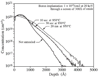
One of the major problems technologists are confronted with, is the realization of ultra-thin junctions, of depths of several tens of nanometers for deep-submicron devices (of gate length lower than 50 nm). The problem is particularly important for P/N junctions, carried out by boron ion implantation. Indeed, the necessary annealing for the dopant activation is accompanied by an abnormally high redistribution of the dopant profile. This phenomenon is illustrated in Figure 3.17 (according to [SED 88]), showing the evolution during annealing at 950°C of boron profiles implanted in Si. This figure clearly highlights an important profile redistribution after a 10 second annealing. Such redistribution corresponds to an effective diffusivity exceeding the equilibrium value by several orders of magnitude. On the other hand, we see that the profile remains unchanged for subsequent annealing (the profile at 30 s is almost identical to the profile at 10 s), until the moment when, for definitely more important durations, we find again the normal thermal diffusion process (profile at 20 minutes). These results, confirmed by many other studies, show that this diffusion acceleration is a transient phenomenon. The transient time scale depends on the annealing temperature, with an activation energy close to the self-diffusion temperature (approximately 4.5 – 5 eV) [MIC 86].
Figure 3.17. Transient enhanced diffusion of implanted boron (from [SED 88])
Because of its tremendous technological impact, this phenomenon, known as TED (transient enhanced diffusion), has been studied by many authors. It is now established that this accelerated diffusion is associated with the self-interstitials, created by ion implantation, which survived the direct recombination with the vacancies. In particular, many authors noted a correlation between the transient diffusion and a certain type of interstitial clusters, the “{113}” defects, whose dissolution during annealing seemed to be the self-interstitials source inducing transient diffusion [STO 97]. However, transient diffusion phenomena have also been observed in the absence of {113} defects [ZHA 95], so that the phenomenon is obviously more complex. Meticulous experimental observations of the evolution of the implantation defects, by high-resolution electron microscopy, established that transient diffusion is the result of the self-interstitials supersaturation, created by implantation, but that there is then a competition between the defects out-diffusion towards the surface where they are annihilated, their couplings with boron, the nucleation and then the interstitial clusters evolution. More precisely, various cluster types (simple aggregates, {113}, perfect or faulted stacking faults) are in competition with one another [CLA 03]. Based on these observations, models describing the evolution of these various interstitial clusters are now available. With them, we can follow the temporal evolution of the residual supersaturation of self-interstitials, responsible for the TED phenomenon [LAM 05, ORT 01, ORT 04].
In addition to the enhanced transient diffusion, it was very quickly noted that the redistribution of the implanted boron layers gave way to another phenomenon, a strongly penalizing phenomenon: after the activation annealing, boron is not completely active, even for concentrations lower than its solubility limit. This phenomenon is generally explained by the formation of mixed complexes (clusters) of boron and self-interstitials (BnIm), known as BIC (boron interstitials clusters) [STO 97]. Ab initio theoretical calculations seem to justify the existence of such complexes and give indications on their possible charge states and formation energies according to their composition (n, m) [LEN 00]. The behavior (formation/dissolution) of these BIC also plays a role in the transient diffusion by influencing the kinetics of self-interstitials evolution [BOU 03, BOU 05, COL 01, PIC 06].
From a diffusion modeling point of view, it is possible to take into account the formation/dissolution of the various interstitial clusters and of the corresponding extended defects ({113}, stacking faults), as well as the BIC, by additional terms of generation/recombination in the continuity equations of the various involved species (dopants and point defects) [ORT 01, ORT 04]. It is then possible to obtain completely satisfactory simulations of the redistribution profiles of implanted boron and of activation degree [BOU 03, BOU 05, PIC 06], but with complex numerical calculations demanding high computer resources.
3.4.2. Engineering of ultra-thin junctions
TED phenomena and dopant deactivation described in the previous section are very penalizing for the realization of ultra-thin junctions necessary for the fabrication of the ultimate MOS transistors, for which junction depths of several tens of nanometers only, associated with a very intense dopant activation, are essential. Because of these challenges, several technological approaches are studied to go around these problems. We present below a brief description of the main ideas considered. All these approaches have as common objective to minimize the interactions between boron and self-interstitials.
3.4.2.1. Engineering of point defects
An interesting approach consists of using a high-energy (from several hundred keV to several MeV) silicon implantation before boron implantation. This high-energy implantation creates in the surface area, where the boron is implanted, a zone supersaturated in vacancies, contributing to destroying self-interstitials responsible for TED [NEJ 03]. The suppression of self-interstitials also minimizes the formation of BIC, which leads to better boron activation [SMI 06].
3.4.2.2. Fluorine co-implantation
Several works indicate a clear decrease of the TED when fluorine is co-implanted with the dopant. This was observed for boron [DOW 98, SHA 01], but also for arsenic [LIN 93] and phosphorus [MOG 97]. Nevertheless, the related precise mechanism is not yet clearly established. Although technologically easy to implement in the case of boron (gaseous BF3 is the standard source for implantation), this approach suffers from several negative effects. First of all, it is well-known that the presence of fluorine sensibly accelerates boron diffusion in silica, which leads to integration problems in a complete process flow, because of the increasing risks of boron penetration in the gate oxide or in the spacers. Moreover, some authors indicate that fluorine tends to deactivate boron [DRO 03, SHA 01].
3.4.2.3. Carbon co-implantation
Carbon being an inevitable residual impurity of Cz silicon, its behavior in silicon has been studied for a long time (see [KIM 89] for the main results). Among the many possible reactions, substitutional carbon (Cs) can be ejected from its stable site by reaction with a self-interstitial to form an interstitial carbon (CI). This carbon interstitial, itself mobile, reacts in its turn with another substitutional carbon, to form an immobile pair CICS. This behavior makes carbon an effective trap for self-interstitials and a potential candidate to reduce TED. This was experimentally demonstrated and studied in detail in the case of boron [CAG 08, PAW 06a] and phosphorus [CAG 07, CAG 08, KU 06, PAW 06b], implanted in pre-amorphized Si by germanium implantation (PAI). It results from these studies that, thanks to an optimization of the placement (implantation energy) and of the carbon dose used, it is possible to completely remove the boron and phosphorus transient diffusion, as shown in Figure 3.18 [CAG 08].
Figure 3.18. Influence of co-implanted carbon on the form of boron (a) and phosphorus (b) profiles — according to [CAG 08]
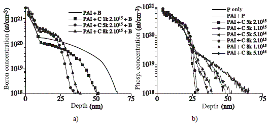
Figure 3.18b, relative to phosphorus, highlights the fact that by an optimized selection of the experimental conditions, selection based on the specific mechanisms of the P diffusion described previously, it is possible to completely eliminate the accelerated phosphorus diffusion tail. It is thus possible to obtain, with this impurity, profiles as abruptly as with arsenic [CAG 07, CAG 08]. This has an unquestionable advantage insofar as phosphorus being a lighter impurity, its implantation introduces less defects than arsenic, which can be crucial for ultimate technologies, using increasingly lower thermal budgets, for which the residual defect annealing is a true challenge.
3.4.3. Reverse short channel effect
This example is given to illustrate the technological importance of the diffusional coupling phenomena, via defect gradients for the optimization of strongly submicron devices. Let us recall that the threshold voltage of a MOS transistor controlled among other things by the concentration of the dopant present in the channel zone located right under the gate oxide, varies with the device length (lateral distance between the source and drain zones). Purely electrostatic considerations imply that this threshold voltage, all other things being equal, must decrease along with a diminution of the MOS length. This is due to the fact that the width of depletion zones induced by the drain and source junctions are no longer negligible in front of the MOS length, so that the quantity of substrate carriers to be “evacuated” by gate polarization is reduced for small size devices. On the other hand, experimental results show in most cases an increase in the threshold voltage, with a decreased gate length, before the expected natural drop. This reverse short channel effect (RSCE) can only be explained by considering disturbances of the channel doping profile induced by the fabrication step of the sources/drains [RAF 93].
Indeed, these junctions are manufactured by ion implantation of a high-dose dopant (in general As for a N-MOS), followed by an activation annealing. During this activation annealing, excess self-interstitials introduced by implantation evolve in a complex way, as described previously. This being said, the diffusion length of the free defects is relatively important, so that the interstitials supersaturation spreads over distances largely exceeding the junctions areas. There is in particular a very strong defects injection up to the channel zone, where they will induce considerable effects on the present dopant atoms (boron for an N-MOS).
Let us consider a vertical section of the device at an abscissa point z along the channel (see Figure 3.19a). In the bulk there is a self-interstitial supersaturation coming from the source and drain zones, whereas the surface maintains the thermal equilibrium concentration . There is thus a strong defects gradient between the bulk and the surface. This gradient (“defect wind”) necessarily induces a boron atoms diffusion towards the surface (see section 3.3.3.2, equation [3.54]), so that even if the boron profile is initially flat, the final profile will show a boron accumulation at the surface (see Figure 3.19a). However, the level of self-interstitials supersaturation coming from source and drain zones vary with z along the channel, and the phenomenon intensity thus varies along the channel. We thus reach an inhomogeneous distribution of the boron concentration profile, as schematized on Figure 3.19b, showing a longitudinal section along the channel, at the close proximity of the interface. Using this figure, we easily understand the appearance of the reverse short channel effect. If the channel is long enough, the distance (δl) affected by the lateral disturbance of the boron concentration is negligible. The average dopant concentration in the channel is not changed and the threshold voltage is not affected. On the other hand, with the size decrease of the device, all other things being equal, this transition zone is no longer negligible, and the average channel doping increases, involving an increase in the threshold voltage, as experimentally observed.
Figure 3.19. Schematic section of the dopants and defects profiles in the channel zone during the activation annealing of the implanted junctions: (a) vertical section in the proximity of the source junction; (b) longitudinal section in the proximity of the interface with gate oxide

3.5. Dopant diffusion in germanium
Given up for long years due to the benefit of silicon for traditional MOS technologies (the Si/SiO2 interface being the most powerful), the use of germanium is again considered for the ultimate devices. Indeed, the best mobility of charge carriers in this material is an interesting idea for faster devices, which in any event will have to use a gate dielectric different from SiO2 (dielectric with strong permittivity) [ITR 09]. The optimization of these devices will thus go through a good control of the technology of this “new” material. In particular, it will be necessary to have efficient models able to precisely describe dopant diffusion in germanium, to feed the simulation software for technological computer aided design (TCAD tools).
Unfortunately, the basic studies on germanium were given up at the beginning of the 1960s, after the advent of silicon, and have only very recently begun again. Consequently, the theoretical understanding degree on dopant diffusion in Ge and the availability of efficient simulation models, is still far from what is at the disposal of technologists for silicon. The aim of this section, which does not claim to be exhaustive, is to give a short review of the state of knowledge, still partial, on this topic.
3.5.1. Thermal diffusion process
The first experimental pieces of data concerning the thermal diffusion process of common dopants in germanium is from the 1950s. A complete study, using the available techniques of the time, was carried out by W.C. Dunlap [DUN 54]. He measured the donors (Sb, As, P) and acceptors (Ga, Al, In and B) diffusion in the range of 650 — 900°C, using radioactive tracers and the p-n junction method. These first results indicate a definitely faster diffusion of the donors than the acceptors, with values of the diffusion coefficient at 700°C, of about 10-14 cm2s-1 for boron and gallium, 10-12 cm2s-1 for phosphorus and 6.5x10⁻¹² cm2s-1 for arsenic. Another outstanding fact is that all the dopants have about the same activation energies of diffusion (about 2.5 eV), except for boron which has a definitely higher activation energy. This is not figured in the article of W.C. Dunlap, which allocated this difference to an experimental problem. This 2.5 eV energy is significantly lower than the activation energy of germanium self-diffusion, about 3 eV [LET 56, VOG 83, WER 85]. This highlights a considerable attractive binding energy between these dopants and the defect responsible for diffusion. More recent data, taking advantage of more sophisticated investigation means, such as secondary ions mass spectrometry (SIMS), can give precise determinations of the dopant profiles and lead to a more precise image of the experimental reality. The main results are summarized below.
3.5.1.1. Self-diffusion
All the experimental pieces of data available lead us to conclude almost certainly that germanium self-diffusion takes place by a vacancy mechanism. The most convincing study is from Mr. Werner et al., analyzing the influence of doping and of the hydrostatic pressure on the self-diffusivity of germanium [WER 85]. In this study, these authors confirmed that the self-diffusivity of Ge varies with the doping concentration, consistently with the existence of an acceptor level for the vacancy. They also clearly highlighted that the germanium self-diffusivity decreases with pressure. This last result, corresponding to a positive activation volume, is the signature of a vacancy mechanism.
This conclusion is in addition completely consolidated by the ab initio theoretical calculations concerning the formation and migration energies of the elementary defects (vacancy and self-interstitial) in Ge. The most recent outcomes [VAN 07] give, for the neutral defects, a formation energy of 2.35 (± 0.1) eV for the vacancy and of 3.25 (± 0.25) eV for the self-interstitial. The calculated migration energies are respectively about 0.6 (± 0.1) eV for the vacancy and approximately twice as much for the self-interstitial. We then reach (see equation [3.30] of section 3.2.2.2) an estimate of 2.95 (±0.2) eV for the activation energy of self-diffusion by the vacancy mechanism (in complete harmony with the experimental value of 3.09 eV [WER 85]), and larger than 4 eV for an interstitial mechanism. It would thus seem that, contrary to the silicon case, the self-interstitial plays a negligible role in germanium self-diffusion.
3.5.1.2. Donors diffusion
An exhaustive study of donor diffusion (P, As and Sb) was recently undertaken by S. Brotzman and H. Bracht in the temperature range of 600 — 920°C, and for various dopants surface concentration [BRO 08]. The main results are as follows:
– the effective diffusion coefficient of the donors varies with the doping level. This behavior of extrinsic diffusion is correctly described by a model implying only singly negatively charged dopant-vacancy pairs (XV-), i.e. doubly negatively charged vacancies (V=). These results seem consistent with the ab initio theoretical calculations concerning the states of charge of the vacancy and the behavior of the dopant-vacancy pairs in Ge [CHR 08, SPI 08];
– the intrinsic diffusion coefficient of these three impurities are significantly higher than the self-diffusivity. At a given temperature, the intrinsic diffusion coefficient increases with the impurity size. For example, at 700°C, the values
obtained are 1.6x10⁻¹⁴ cm2s-1 for P, 3x10-13 cm2s-1 for As and 1x10-12 cm2s-1 for Sb;
– activation energies of the intrinsic diffusion coefficient are lower than the activation energy of the self-diffusion, with slightly different values depending on the dopant, of 2.85 (± 0.04) eV for P, 2.71 (± 0.06) eV for As and of 2.55 (± 0.03) eV for Sb. This decrease with the atom size is naturally interpreted as an increase in the binding energy between the substitutional donor and the vacancy.
It should however be mentioned that the interpretation in terms of a mechanism implying exclusively doubly negative vacancies, has not yet reached a consensus. Some authors indicate the need to take into account interactions with neutral vacancies and doubly negatively charged vacancies to correctly describe the arsenic profiles redistribution [VAI 00]. Moreover, recent simulation attempts of the redistribution of phosphorus profiles on the basis of an interaction with doubly negatively charged vacancies, with or without accounting for neutral vacancies, were unsuccessful [CAN 08]. However, very good adjustments were obtained by taking into account a contribution of the triply charged vacancies, introducing a cubic variation of the effective diffusivity with the free electrons concentration [CAN 10]. Other authors, on the basis of the influence of the pressure on the implanted profiles redistribution, even challenge the vacancy mechanism for arsenic diffusion [MIT 96]. It is thus clear that complementary studies are to be done to definitively clarify the atomic diffusion mechanisms of the donors in germanium.
3.5.1.3. Boron diffusion
The most recent studies concerning boron diffusion in germanium lead to extremely low diffusivity values, about 10-17 to 10-15 cm2s-1, for temperatures between 800 and 900°C [UPP 04]. Correlatively, the activation energy is about 4.6 eV, much higher than the self-diffusion energy. Such a difference in activation energies results in thinking that the elementary diffusion mechanisms (implied point defects) are not similar, which seems to indicate that boron diffusion, contrary to the donors case, would primarily be assisted by self-interstitials [UPP 04]. Nevertheless, at this stage, we cannot completely exclude the hypothesis of a vacancy mechanism with a very strong repellent interaction (negative binding energy) between the vacancy and the boron atom. Such a repellent interaction, but at a less important degree, is for example invoked to explain why silicon, isoelectronic impurity, diffuse in germanium with an activation energy higher than the self-diffusion energy, but via a vacancy mechanism [SIL 06].
3.5.2. Implanted dopants and junctions engineering
In addition to the fundamental studies, briefly summarized above, the possible interest of germanium as a basic material for upcoming technological CMOS generations has also motivated studies aiming to find a way to the fabrication of good quality junctions, using common microelectronics techniques, i.e. by ion implantation followed by an activation annealing. The interested reader will find an excellent summary of the main issues and results in an article by E. Simoen et al. [SIM 06] briefly summarized below.
3.5.2.1. P+/N junctions
Despite a rather low solubility limit of chemical boron in germanium, lower than 1019 cm-3 [JON 87], it has been proved rather simple to elaborate P+ layers by ion boron implantation, having a sufficient conductivity to manufacture efficient devices. On the one hand, this is due to the very low diffusivity of B, as previously indicated, preventing the redistribution of the implanted profile during activation annealing. On the other hand, this is also due to a dynamic annealing phenomenon leading to dopant self-activation during implantation [JON 87]. It is even possible to reach total boron activation by ion implantation at room temperature, without subsequent annealing [UPP 01]. Thermal annealing can then reach active concentrations beyond the limit of boron solubility. Active concentrations of a few 1020 cm-3 are easily reachable by RTA (rapid thermal annealing).
In addition, it was shown that it was possible to further increase the active boron concentration, up to a level close to 5 x 1020 cm-3, by a simple annealing at 400°C of a profile implanted in germanium pre-amorphized by high-dose Ge ion implantation [CHA 05]: during the solid phase epitaxy, leading to germanium recrystallization, boron atoms are trapped in substitutional sites. Although these solid solutions are supersaturated in boron, they prove rather stable and resist to 60 seconds annealing at 600°C [SIM 06], which is sufficient considering the thermal budget planned for ultimate MOS technologies. This should probably be correlated with the very low boron diffusivity, leading to very slow kinetics for reactions in solid phase (like germination or precipitates growth) involving this impurity. Nevertheless, the defects created by implantation and pre-amorphization are eliminated with difficulty by these annealings with low thermal budget [SIM 05]. A compromise thus still remains to be found to obtain acceptable leakage currents.
3.5.2.2. N+/P junctions
Due to their atomic mass being higher than that of boron, donor (P, As, Sb) ion implantation, at the doses required by the technology, induces very significant damage of the germanium substrate, generally leading to the formation of an amorphized P type surface layer [BEN 92]. The restoration of the crystalline quality and the activation essential to the making of the N+ layer then require annealing with high thermal budgets. In the case of antimony, the damage is too important to be efficiently annealed: there is in fact a formation of cavities resulting from the vacancies clustering created by implantation [JAN 06]. For arsenic, the problem is a little less important, but generally the annealed layers have a very important surface roughness [JAN 06].
Because of that, phosphorus proves to be the best applicant for the creation of N+/P junctions. Nevertheless, the realization of efficient junctions by phosphorus implantation and annealing still faces a certain number of difficulties, summarized below:
– an important outdiffusion (dopant evaporation from the surface) occurs during the activation annealing, leading to a very strong dose loss of the dopant [CAN 08, POO 85]. An adequate encapsulation (SiO2) minimizes this problem, but does not completely avoid it;
– a very fast phosphorus diffusion in extrinsic condition leads to a significant broadening of the implanted profile, which raises the problem of the ultra-thin junctions necessary for the upcoming technological generations;
– the electrically active phosphorus concentration saturates at rather low values of several 1019 cm-3, even for strong implantation doses. The origin of this difference between the active concentration and the chemical solubility is not yet perfectly solved.
In order to get around these difficulties, various technological approaches are studied, like laser annealing for better dopants activation (incorporation beyond the equilibrium limit) [TSO 06] or defect engineering following a logic similar to the one applied for silicon [SIM 06].
Therefore, we can note that the development of well-established technology for the creation of operational junctions in germanium still requires more thorough research. Moreover, the essential studies remain to be completed to lead to models of dopant diffusion in Ge suitable for reliable technological simulations. This will be made possible, like in the case of silicon, by the understanding and modeling of the couplings between dopants and (point or complex) defects of the material.
3.6. Conclusion
Throughout this chapter, emphasis was put on the need, for a proper model of dopant diffusion in silicon and for the optimization of junction engineering, to take into account increasingly complex couplings phenomena between dopant atoms and material point defects. In particular, the few examples developed in section 3.4 show the extreme importance of these couplings phenomena in the determination of the real dopant profiles inside the structure of the devices, and thus in fine on the device electric characteristics.
Moreover, it is obvious that with the systematic reduction of the device size, a simple 1D description is no longer sufficient, the 2D, or even 3D simulations, becoming essential for a description of experimental realities (the short reverse channel effect is a typical example of this fact). We thus understand why the optimization of the elementary devices is increasingly demanding regarding the modeling of dopant diffusion, in order to have reliable predictive tools in the domain of technological simulation.
3.7. Bibliography
[BEN 92] BENOURHAZI K., PONPON J.P., “Implantation of phosphorus and arsenic ions in germanium”, Nuclear Instruments and Methods in Physics Research Section B, no. 71, p. 406–411, 1992.
[BLA 72] BLANCHARD B. et al., “Compte-rendu du colloque Caractérisation des matériaux et des technologies des semi-conducteurs”, Grenoble, 1972.
[BOU 03] BOUCARD F., Modélisation de la diffusion des dopants dans le silicium pour la réalisation de jonctions fines, PhD Thesis, Louis Pasteur University, Strasbourg, 2003.
[BOU 05] BOUCARD F., ROGER F., CHAKAROV I., ZHUK V., TEMKIN M., MONTAGNER X., GUICHARD E., MATHIOT D., “A comprehensive solution for simulating ultra-shallow junctions: from high dose/low energy implant to diffusion annealing”, Materials Science Engineering B, no. 124, p. 409–414, 2005.
[BRO 08] BROTZMANN S., BRACHT H, “Intrinsic and extrinsic diffusion of phosphorus, arsenic, and antimony in germanium”, Journal of Applied Physics, no. 103, p. 033508, 2008.
[CAG 07] CAGNAT N., MATHIOT D., LAVIRON C. J., “Ultrathin n+/p junction in preamorphized silicon by phosphorus and carbon coimplantation engineering: influence of C location”, Journal of Applied Physics, no. 102, p. 106102, 2007.
[CAG 08] CAGNAT N., Implantation ionique et jonctions fines — Caractérisation, ingénierie des défauts et application aux technologies 65 et 45 nm, PhD Thesis, Louis Pasteur University, Strasbourg 1, 2008.
[CAN 08] CANNEAUX T., MATHIOT D., ROQUES S., SCHMITT S., DUBOIS C. “Diffusion of phosphorus implanted in germanium”, Materials Science Engineering B, no. 154, p. 68–71, 2008.
[CAN 10] CANNEAUX T., MATHIOT D., PONPON J.P., LEROY Y., “Modeling of phosphorus diffusion in Ge accounting for a cubic dependence of the diffusivity with the electron concentration”, Thin Solid Films, no. 518, p. 2394–2397, 2010.
[CAR 59] CARSLAW H.S., JAEGER J.C., Conduction of Heat in Solids, Clarendon Press, Oxford, 1959.
[CHA 05] CHAO Y.L., PRUSSIN S., WOO J.C.S., SCHOLZ R., “Preamorphization implantation-assisted boron activation in bulk germanium and germanium-on-insulator”, Applied Physics Letters, no. 87, p. 142102, 2005.
[CHR 08] CHRONEOS A., BRACHT H., GRIMES RW., UBERUAGA B.P., “Vacancy-mediated dopant diffusion activation enthalpies for germanium”, Applied Physics Letters, no. 92, p. 172103, 2008.
[CHU 05] CHUI C.O., KULIG L., MORAN J., TSAI W., SARASWAT K.C., “Germanium n-type shallow junction activation dependences”, Applied Physics Letters, no. 87, p. 091909, 2005.
[CLA 03] CLAVERIE A., COLOMBEAU B., DE MAUDUIT B., BONAFOS C., HEBRAS X., BEN ASSAYAG G., CRISTIANO F., “Extended defects in shallow implants”, Applied Physics Letters A, no. 76, p. 1025–1033, 2003.
[COL 01] COLOMBEAU B., SMITH A. J., COWERN N. E. B., PAWLAK B. J., CRISTIANO F., DUFFY R., CLAVERIE A., ORTIZ C. J., PICHLER P., LAMPIN E., ZECHNER C., “Current Understanding and Modeling of B Diffusion and Activation Anomalies in Preamorphized Ultra-Shallow Junctions”, in P. PICHLER, A. CLAVERIE, R. LINDSAY, M. ORLOWSKI, W. WINDL (eds), Silicon Front-End Junction Formation — Physics and Technology, Materials Research Society Symposium Proceedings, no. 810, p. C3.6.1, 2001.
[CRA 75] CRANCK J., The Mathematics of Diffusion, 2nd edition, Clarendon Press, Oxford, 1975.
[DOW 98] DOWNEY D.F., CHOW J.W., ISHIDA E., JONES K.S., “Effect of fluorine on the diffusion of boron in ion implanted Si”, Applied Physics Letters, no. 73, p. 1263–1265, 1998.
[DRO 03] DROBNY V.FF, CHANG K., ROBINSON D., “Activation behavior of BF2+ implants in RTP annealed silicon”, in B. BROWN, T.L. ALFORD, M. NASTASI, M.C. VELLA (eds), 14th Conference on Ion Implantation Technology Proceedings, IEEE, New York, p. 686, 2003.
[DUN 97] DUNHAM M., “Lattice Monte Carlo Simulations of Vacancy-Mediated Diffusion and Aggregation Using Ab Initio Parameters”, in T. DIAZ DE LA RUBIA, S. COFFA, P.A. STOLK, C.S. RAFFERTY (eds), Defects and Diffusion in Silicon Processing, Materials Research Society Symposium Proceedings, no. 469, p. 353–358, 1997.
[DUN 54] DUNLAP JR W.C., “Diffusion of impurities in germanium”, Physics Review, no. 94, p. 1531–1540, 1954.
[FAI 73] FAIR R.B., WEBER G.R., “Effect of complex formation on diffusion of arsenic in silicon”, Journal of Applied Physics, no. 44, p. 273–279, 1973.
[FAI 77] FAIR R.B., TSAI J.C.C., “Quantitative model for diffusion of phosphorus in silicon and emitter dip effect”, Journal of the Electrochemical Society, no. 124, p. 1107–1118, 1977.
[FED 94] FEDOTOV S.A., “Diffusion of electrically active Sb atoms in heavily-doped silicon -Monte-Carlo simulation with regard to collective phenomena”, Physica Status Solidi (b), no. 86, p. 375–382, 1994.
[FRA 56] FRANCK F.C., TURNBULL D., “Mechanism of Diffusion of Copper in Germanium”, Physical Review, no. 104, p. 617–618, 1956.
[GEN 76] DE GENNES P.G., “La percolation: un concept unificateur”, La Recherche, no. 72, p. 919–927, 1976.
[GOS 80] GOSELE U., FRANK W., SEEGER A., “Mechanism an kinetics of the diffusion of gold in silicon”, Appled Physics, no. 23, p. 361–368, 1980.
[HEI 99] HEISER T., ISTRATOV A.A., FLINK C., WEBER E.R., “Electrical characterization of copper related defect reactions in silicon”, Materials Science and Engineering B, no. 58, p. 149–154, 1999.
[HIL 81] HILL C., “Measurement of local diffusion coefficients in planar device structures”, in H.R. HUFF, R.J. KREIGLER, Y. TAKEISHI (eds), Semiconductor Silicon, The Electrochemical Society, Princeton, p. 988–996, 1981.
[HU 74] HU S.M., “Formation of stacking faults and enhanced diffusion in the oxidation of silicon”, Journal of Applied Physics, no. 45, p. 1567–1573, 1974.
[ITR 09] “International Technology Roadmap for Semiconductors”, 2009, available at http://www.itrs.net/.
[JAN 06] JANSSENS T., HUYGHEBAERT C., VANHAEREN D., WINDERICKX G., SATTA A., MEURIS M., VANDERVORST W., “Heavy ion implantation in Ge: Dramatic radiation induced morphology in Ge”, Journal of Vaccum Science and Technology B, no. 24, p. 510–514, 2006.
[JOH 93] JOHN J.P., LAW M.E., “Oxidation enhanced diffusion of phosphorus in silicon in heavily doped background concentrations”, Journal of the Electrochemical Society, no. 140, p. 1489–1491, 1993.
[JON 87] JONES K.S., HALLER E.E., “Ion-implantation of boron in germanium”, Journal of Applied Physics, no. 61, p. 2469–2477, 1987.
[KIM 89] KIMMERLING L.C., ASOM M.T., BENTON, J.L., DREVINSKI P.J., CEFER C.E. “Interstitial defect reaction in Si”, Materials Science Forum, no. 38, p. 141–150, 1989.
[KU 06] KU K.C. et al., “Effects of germanium and carbon coimplants on phosphorus diffusion in silicon”, Applied Physics Letters, no. 89, p. 112104, 2006.
[LAM 05] LAMPIN E., ORTIZ C.J., COWERN N.E.B., COLOMBEAU B., CRISTIANO F., “Combined master and Fokker-Planck equations for the modelling of the kinetics of extended defects in Si”, Solid-State Electronics, no. 49, p. 1168–1171, 2005.
[LEN 00] LENOSKY T.J., SADIGH B., THEISS S.K., CATURLA M.J., DE LA RUBIA T.D., “Ab initio energetics of boron-interstitial clusters in crystalline Si”, Applied Physics Letters, no. 77, p. 1834–1836, 2000.
[LET 56] LETAW H. JR., PORTNOY W.M., AND SLIFKIN L., “Self-diffusion in germanium”, Physics Review, no. 102, p. 636–639, 1956.
[LIN 93] LIN D.G., ROST T.A., “The impact of fluorine on CMOS channel length and shallow junction formation”, International Electron Device Meeting, Washington DC, 1993.
[MAT 82a] MATHIOT D., PFISTER J.C., “Influence of the non-equilibrium vacancies the diffusion of phosphorus into silicon”, Journal of Applied Physics, no. 53, p. 3053–3058, 1982.
[MAT 82b] MATHIOT D., PFISTER J.C., “High-concentration diffusion of P in Si — A percolation problem”, Journal de Physique Lettres, no. 43, p. L453-L459, 1982.
[MAT 83] MATHIOT D., PFISTER J.C., “Diffusion of arsenic in silicon – Validity of the percolation model”, Applied Physics Letters, no. 42, p. 1043–1044, 1983.
[MAT 84] MATHIOT D., PFISTER J.C., “Dopant diffusion in silicon — A consistent view involving non-equilibrium defects”, Journal of Applied Physics, no. 55, p. 3518–3530, 1984.
[MAT 89] MATHIOT D., “Modelling of hydrogen diffusion in n-type and p-type silicon”, Physics Review B, no. 40, p. 5867–5870, 1989.
[MAT 92] MATHIOT D., “Gold, Self-diffusion and dopant diffusion in silicon”, Physics Review B, no. 45, p. 13345–13355, 1992.
[MIC 86] MICHEL A.E., “Diffusion modelling of the redistribution of ion implanted impurities”, in T.O. SEDGWICK, T.E. SEIDEL, B.Y. TSAUR (eds), Rapid Thermal Processing, Materials Research Society Symposium Proceedings, no. 52, p. 3–13, 1986.
[MIT 96] MITHA S., AZIZ M.J., SCHIFERL D., POKER D.B., “Activation volume for arsenic diffusion in germanium”, Applied Physics Letters, no. 69, p. 922–924, 1996.
[MIY 85] MIYAKE M., “Oxidation-enhanced diffusion of ion-implanted boron in heavily phosphorus-doped silicon”, Journal of Applied Physics, no. 58, p. 711–715, 1985.
[MOG 97] MOGUL H.C., ROST T.A., LIN D.G., “Advantages of LDD-only implanted fluorine with submicron CMOS technologies”, IEEE Transactions on Electron Devices, no. 44, p. 388–394, 1997.
[NEJ 03] NEJIM A., SEALY B., “Retarding transient enhanced diffusion of boron in silicon with high energy silicon co-implants”, Semiconductor Science and Technology, no. 18, p. 839–844, 2003.
[LAR 93] LARSEN A.N, LARSEN K.K., ANDERSEN P.E., SVENSSON B.G., “Heavy doping effects in the diffusion of group IV and group-V impurities in silicon”, Journal of Applied Physics, no. 73, p. 691–698, 1993.
[ORT 01] ORTIZ C, MATHIOT D., “A new kinetic model for the nucleation and growth of interstitial clusters in silicon”, in M.A. FOAD, J. MATSUO, P. STOLK, M.D. GILES, K.S. JONES (eds), Si Front-End Processing — Physics and Technology of Dopant-Defect Interactions III, Materials Research Society Symposium Proceedings, no. 669, p. J5.6.1, 2001.
[ORT 04] ORTIZ C.J., PICHLER P., FUHNER T., CRISTIANO F., COLOMBEAU B., COWERN N.E.B., CLAVERIE A., “A physically based model for the spatial and temporal evolution of self-interstitial agglomerates in ion-implanted silicon”, Journal of Applied Physics, no. 96, p. 4866–4877, 2004.
[PAW 06a] PAWLAK B.J., JANSSENS T., BRIJS B., VANDERVORST W., COLLART E.J.H., FELCH S.B., COWERN N.E.B., “Effect of amorphization and carbon co-doping on activation and diffusion of boron in silicon”, Applied Physics Letters, no. 89, p. 062110, 2006.
[PAW 06b] PAWLAK B.J., DUFFY R., JANSSENS T. VANDERVORST W., FELCH S.B., COLLART E.J.H., COWERN N.E.B., “Suppression of phosphorus diffusion by carbon co-implantation”, Applied Physics Letters, no. 89, p. 062102, 2006.
[PHI 91] PHILIBERT J., Atom Movements. Diffusion and Mass Transport in Solids, Editions de Physique, Les Ulis, 1991.
[PIC 06] PICHLER P. et al., “Diffusion and activation of dopants in silicon and advanced silicon-based materials”, Physica Scripta, no. T126, p. 89–96, 2006.
[POO 05] POON C.H., TAN L.S., CHO B.J., DU A.Y., “Dopant loss mechanism in n+/p germanium junctions during rapid thermal annealing”, Journal of the Electrochemical Society, no. 152, p. G895-G899, 2005.
[QUO 72] QUOIRIN J.B., Détermination de profil de diffusion de bore dans le silicium à l’aide de l’analyseur ionique Castaing-Slodzian, PhD Thesis, Grenoble University, 1972.
[RAF 93] RAFFERTY C.S., VUONG H.H., ESHRAGHI S.A., GILES M.D., PINTO M.R., HILLENIUS S.J., “Explanation of reverse short channel effect by defect gradients”, International Electron Device Meeting, Washington DC, 1993.
[SED 88] SEDGWICK T.O., MICHEL A.E., DELINE V.R., COHEN S.A., LASKY J.B., “Transient boron-diffusion in ion-implanted crystalline and amorphous silicon”, Journal of Applied Physics, no. 63, p. 1452–1463, 1988.
[SHA 01] SHANO T., KIM R., HIROSE T., FURUTA Y., TSUJI H., FURUHASHI M., TANIGUCHI K., “Realization of ultra-shallow junction: suppressed boron diffusion and activation by optimized fluorine co-implantation”, International Electron Device Meeting, Washington DC, 2001.
[SIL 06] SILVESTRI H.H., BRACHT H., HANSEN J.L., LARSEN A.N., HALLER E.E., “Diffusion of silicon in crystalline germanium”, Semiconductor Sciences and Technology, no. 21, p. 758–762, 2006.
[SIM 05] SIMOEN E., SATTA A., MEURIS M., JANSSENS T., CLARYSSE T., BENEDETTI A., DEMEURISSE C., BRIJS B., HOFLIJK I., VANDERVORST W., CLAEYS C., “Defect removal, dopant diffusion and activation issues in ion-implanted shallow junctions fabricated in crystalline germanium substrates”, Solid State Phenomena, no. 108–109, p. 691–696, 2005.
[SIM 06] SIMOEN E. et al., “Ion-implantation issues in the formation of shallow junctions in germanium”, Material Science in Semiconductor Processing, no. 9, p. 634–639, 2006.
[SMI 06] SMITH A.J., COWERN N.E.B., GWILLIAM R, SEALY B.J., COLOMBEAU B., COLLART E.J.H., GENNARO S., GIUBERTONI D., BERSANI M., BAROZZI M., “Vacancy-engineering implants for high boron activation in silicon on insulator”, Applied Physics Letters, no. 88, p. 082112, 2006.
[SPI 08] SPIEWAK P., VANHELLEMONT J., SUEOKA K., KURZYDLOWSKI K.J., ROMANDIC I., “First principles calculations of the formation energy and deep levels associated with the neutral and charged vacancy in germanium”, Journal of Applied Physics, no. 103, p. 086103, 2008.
[STO 97] STOLK P.A., GOSSMANN H.J., EAGLESHAM D.J., JACOBSON D.C., RAFFERTY C.S., GILMER G.H., JARAIZ M., POATE J.M., LUFTMAN H.S., HAYNES T.E., “Physical mechanisms of transient enhanced dopant diffusion in ion-implanted silicon”, Journal of Applied Physics, no. 81, p. 6031–6050, 1997.
[TSO 06] TSOUROUTAS P., TSOUKALAS D., FLORAKIS A., ZERGIOTI I., SERAFETINIDES A.A., CHERKASHIN N., MARTY B., CLAVERIE A., “Laser annealing for n+/p junction formation in germanium”, Material Science in Semiconductor Processing, no. 9, p. 644–649, 2006.
[TUC 74] TUCK B., Introduction to Diffusion in Semiconductors, IEE monograph series 16, Peter Peregrinus Ltd, Stevenage, 1974.
[UPP 01] UPPAL S., WILLOUGHBY A.F.W., BONAR J.M., EVANS A.G.R., COWERN N.E.B., MORRIS R., DOWSETT M.G., “Diffusion of ion-implanted boron in germanium”, Journal of Applied Physics, no. 90, p. 4293–4295, 2001.
[UPP 04] UPPAL S., WILLOUGHBY A.F.W., BONAR J.M., COWERN N.E.B., GRASBY T., MORRIS R.J.H., DOWSETT M.G., “Diffusion of boron in germanium at 800–900 degrees C”, Journal of Applied Physics, no. 96, p. 1376–1380, 2004.
[URA 99] URAL A., GRIFFIN P., PLUMMER J.D., “Fractional contributions of microscopic diffusion mechanisms for common dopants and self-diffusion in silicon”, Journal of Applied Physics, no. 85, p. 6440–6446, 1999.
[VAI 00] VAINONEN-AHLGREN E., AHLGREN T., LIKONEN J., LEHTO S., KEINONEN J., LL W., HAAPAMAA J., “Identification of vacancy charge states in diffusion of arsenic in germanium”, Applied Physics Letters, no. 77, p. 690–692, 2000.
[VAL 57] VALENTA M.W., RAMASASTRY C., “Effect of heavy doping on the self-diffusion of germanium”, Physics Review, no. 106, p. 73–75, 1957.
[VAN 07] VANHELLEMONT J., SPIEWAK P., SUEOKA K., “On the solubility and diffusivity of the intrinsic point defects in germanium”, Journal of Applied Physics, no. 101, p. 036103, 2007.
[VOG 83] VOGEL G., HETTICH G., MEHRER H., “Self-diffusion in intrinsic germanium and effects of doping on self-diffusion in germanium”, Journal of Physics C: Solid State Physics, no. 16, p. 6197–6204, 1983.
[WAT 64] WATKINS G.D., CORBETT J.W., “Defects in irradiated silicon: electron paramagnetic resonance and electron-nuclear double resonance of the Si-E center”, Physics Review, no. 134, p. A1359-A1377, 1964.
[WER 85] WERNER M., MEHRER H., “Effect of hydrostatic pressure, temperature, and doping on self-diffusion in germanium”, Physics Review. B, no. 32, p. 3930–3937, 1985.
[WIL 77] WILLOUGHBY A.F.W., “Interactions between sequential dopant diffusion in silicon -Review”, Journal of Physics. D, no. 10, p. 455–480, 1977.
[YOS 74] YOSHIDA M., ARAI M., NAKAMURA H., TERUNUMA Y., “Excess vacancy generation mechanism at phosphorus diffusion into silicon”, Journal of Applied Physics, no. 45, p. 1498–1506, 1974.
[ZHA 95] ZHANG L. H., JONES K. S., CHI P. H., SIMONS D. S., “Transient enhanced diffusion without {311} defects in low energy B+-implanted silicon”, Applied Physics Letters, no. 67, p. 2025–2027, 1995.
1Chapter written by Daniel MATHIOT.