
Chapter 2
Ion Implantation 1
2.1. Introduction
Ion implantation consists of introducing charged atoms (projectiles) into a material (the target), by communicating to them sufficient energy so that they enter beyond the surface area. The projectiles’ energy is thus clearly different from those of techniques aiming for a surface process or deposition (plasma, molecular beam). Moreover, the implantation is distinguished from these other methods by the purity of the beam, selected at the isotopic level.
It is essentially thanks to the semiconductor industry that implantation technology could spread. Ion implantation is indeed the most common method of semiconductors doping1. Nowadays, there are thousands of ion implantation machines functioning in this industry. Most of them are devoted to the production of integrated circuits based on silicon. The method, which in the 1970s definitively led to ion implantation supplanting diffusion in the manufacturing technology of microelectronics devices, is the adjustment of the threshold voltage of MOS transistors.
Once incorporated in the process and because of its advantages, implantation quickly imposes itself into all the other doping stages, and even in processes of insulation or purification of the silicon: formation of drain and source areas and the deep n- or p-wells of CMOS circuits, the realization of burred collectors, emitter and base doping in bipolar technology, impurity gettering, realization of buried insulating silica layers by implantation of an important quantity of oxygen, etc. Nowadays, for example, the fabrication of the circuits of the most recent CMOS technology requires more than ten stages of ion implantation.
The main advantage of implantation is the precise control of the number and of the penetration depth of the ions. Although the word is incorrect (we should say fluence), the dose indicates the number of ions implanted per unit of surface of the target (often given in atoms/cm2) and the energy of ions (generally in keV) is the parameter controlling the spatial distribution of the atoms. Implantation is often employed as a technique of pre-deposition, only used to introduce a specific dose in the target. It is by diffusion that the dopants are then redistributed on distances that we cannot reach with implantation.
The major disadvantage of the technique is the inevitable damaging of the target during the slowing down of the ions. The collisions of the projectiles with the atoms of the target move the latter from their initial equilibrium position. If the atom thus displaced acquires enough energy, it can cause other displacements, and be at the origin of a cascade of collisions. The damage created by the implantation must be repaired (we speak of healing), before being able to profit from the effects expected from implantation, i.e. full electrical activity of the dopants. This healing intervenes during a thermal treatment (annealing), following the implantation. During annealing, some diffusion of the implanted species is inevitable. Therefore, whatever the terms of use of the technique (pre-deposition followed by diffusion, or implantation followed by annealing), implantation and diffusion are inseparably linked.
Another advantage of the implantation, less important than the first on the technological level, but interesting in some situations, lies in the fact that it is an athermal process: the quantity of atoms that we can introduce into a target is not submitted to the laws of thermodynamics. In other words, the solubility limit can be largely exceeded; the only limit coming, possibly, from the phenomenon of surface sputtering. However, this advantage is very relative because, during annealing, the thermodynamic equilibrium reasserts itself, often causing the precipitation of a significant part of the implanted species. However, some precautions during these annealings — low temperatures and/or very short durations — help us to maintain these non-equilibrium situations. Of course, these limited thermal budgets also lead to the minimization of the dopant redistribution: it explains the appearance of the “rapid” thermal annealing techniques, using high power lasers or lamps.
All the aspects quickly mentioned in this introduction — ion path, damaging, annealing, dopant activation, application to the development of devices — will be developed in this chapter. Before this, a section will be devoted to the description of implantation machines (in short, implanters).
Abundant literature exists in this domain, notably in the proceedings of the semiannual IBMM (Ion Beam Modification of Materials) and IIT (Ion Implantation Technology) conferences. In addition, several books have been devoted to ion implantation. Some of them are referred to: [DEA 73, FAV 93, RYS 82, WIL 84, ZIE 92].
2.2. Ion implanters
2.2.1. General description
Depending on their use in the various fields of microelectronics, implanters are classified into two categories: the medium current implanters (a few mA at maximum) and high current implanters (from a few mA up to several tens of mA). The range of accessible energy is the same in the two categories, typically from 10 to 200 keV. The difference between the two groups lies in their process capacity and in their respective flexibility in use. A medium current implanter processes one wafer at a time. The ions are distributed there uniformly with the help of a system of electrostatic scanning. The sample holder can often be oriented, which is useful for oblique implantations. The limitation in current is related to the difficulty in evacuating, as calories, a sufficient quantity of the energy deposited by the beam. On a high current implanter, typically several tens of targets are installed on a carousel revolving permanently in front of the beam. This target displacement constitutes one of the scanning directions, the other being of an electrostatic or mechanical nature.
In this configuration, heating problems under the beam are less severe. Figure 2.1 schematically illustrates the general disposition of a medium current implanter.
An ion implanter consists of a source of ions into which the elements to be ionized are introduced in the form of gas or vapor. With a polarized electrode, we can extract ions from the source. A magnetic analysis system separates the ions according to their mass and an acceleration column communicates to them the desired speed. Lastly, a set of polarized plates uniformly distributes the ions on the target. The loading of the wafers and their positioning in front of the beam and then their unloading are executed by a robotized system. On a medium current implanter, with the master controller of the target we can often tilt the wafers up to 60 degrees in relation to the direction of the beam. It is an interesting method for some applications in microelectronics. On a high current implanter, the flexibility is less important: the targets are simply tilted by a few degrees compared to the normal, in order to avoid the channeling phenomenon of ions (see section 2.3.3).
Figure 2.1. Schematic representation of a medium current ion implanter
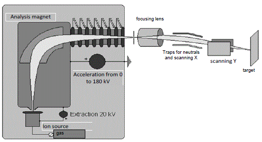
There is a third category of implanters, much less common than the other two. This category comprises the high-energy machines, obviously set aside for more deep processing. These machines are often equipped with Van De Graaff voltage generators, immersed in a tank filled with gas under pressure. The ions are accelerated there, typically at energies of about a few MeV. They are more expensive and more complex to use, and thus more rare.
2.2.2. Ion sources
An ion source essentially consists of a closed vessel, called an arcing chamber, in which an electrical discharge is maintained in a gas or in a vapor containing the desired element. In most high current sources, the discharge is initiated and maintained by electrons emitted by a filament heated by the transit of an intense current and by a magnetic field, perpendicular to the direction of electron emission, which considerably increases their course between the cathode and anode. Thus, the probability of ionizing the vapor atoms increases by a significant factor. The source with a Freeman hot cathode is very frequently used in industrial implanters [FRE 63]. In this type of source, a voltage of about 50–100 V is applied between the cathode and anode and the intensity of the magnetic field is about 100 G. The efficiency of this source is due to the position of the cathode, parallel and very close to the extraction electrode, which produces an intense discharge at a very favorable location. In the sources with cold cathode, the discharge is maintained with the help of higher voltages and magnetic fields, respectively 1 to 2 kV and a few kG. Other methods can be used to maintain a discharge or to ionize the elements: the implementation of a field of high or very high frequency in the microwave or ECR (electron cyclotron resonance) HF (high frequency), sources, phenomena of surface sputtering and ionization in the sources with sputtering [STE 92].
Most elements are introduced into the arcing chamber in the form of a pure gas or as components of gaseous molecular compounds. Other elements, liquid or solid, with a vapor pressure of about 10-3 Torr in a controllable temperature range (300–700°C), are set in a furnace close to the arcing chamber. Sometimes, solids, which cannot be vaporized in the elementary form, exist in the form of compounds, which can often be more easily sublimed. Lastly, low vapor pressure materials can be vaporized using a chemical reaction. The method consists of, in the furnace mentioned above, making a highly reactive gas (fluorine, chlorine) transit on the material, pure or in oxide state, to form a more volatile fluoride or chloride.
2.2.3. Mass analysis and beam optics
A large amount of ions, monoatomic or molecular, with different masses or charge states, is extracted from the source. For example, when boron trifluoride is injected into the arcing chamber, the ions extracted from the source are: 10B++, 11B++, 10B+, 11B+, F+, 10BF+, 11BF+, 10BF2+, 11BF2+, 10BF3+, 11BF3+
. For each ion group, their intensities are in the isotopic abundance, namely 1 to 5, in the case of boron 10 and 11. Only one type of ion generally interests the user, for example 11B+. It is thus necessary to proceed to a selection according to the mass of these ions. An analysis magnet separates the various beams. Indeed, the path of the ions, accelerated by a potential V (in volts), follows, in a magnetic field B (in Gauss), a circle trajectory of radius R (in centimeters) so that ![]() where M1 is the mass of the ion (in atomic units) and n its charge state. The common magnets installed in the implanters have average resolutions of about M1/ΔM1≈100. This means that they are able to differentiate the ion of mass 100 from the ion of mass 101. In the range of the common beams of microelectronics technology, a good resolution in mass is essential to separate for example 11BF+from31P+. In some situations, the separation is impossible and contaminations are feared, for example 27Al+ and 11B0+.
where M1 is the mass of the ion (in atomic units) and n its charge state. The common magnets installed in the implanters have average resolutions of about M1/ΔM1≈100. This means that they are able to differentiate the ion of mass 100 from the ion of mass 101. In the range of the common beams of microelectronics technology, a good resolution in mass is essential to separate for example 11BF+from31P+. In some situations, the separation is impossible and contaminations are feared, for example 27Al+ and 11B0+.
Most installations have a magnet deflecting the ion trajectory at 90 degrees. Under these conditions, the magnets also have a significant focusing role: the image of the extraction slot is located at the same distance from the output pole of the magnet, as the source from the input pole. It is there that a shutter is often set (a Faraday cage or a definition slot) allowing us to control the beam or to stop the undesirable ions. Beyond this point, the beam is again divergent. It is taken back a little further in quadripolar electromagnetic lenses, which refocus it before its entrance into the scanning plates.
2.2.4. Current measurement
Implantation stations, different on medium and high current implanters, have been broadly described in section 2.2.1. An important aspect of the design of these chambers relies in measuring the current, and thus the dose. Generally, on medium current implanters, the target is directly connected to an ammeter and the current is integrated there, in order to determine the dose ϕ, according to the relation:
[2.1]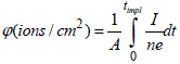
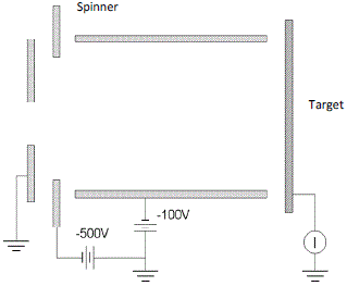
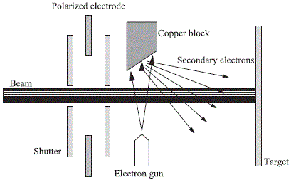
where A (in cm2) is the implanted surface, usually defined by a beam limiter at the entrance of the implantation chamber. I (in ampere) is the beam current, and e is the elementary charge (in coulomb). timpl corresponds to the entire duration of the implantation. A certain number of phenomena possibly come to distort this measurement: (1) the ions, on their course to the target, can capture an electron and thus be found in a neutral state; (2) the impact of the ions tears off electrons from the target which, if they do not go back there, give place to a parasitic surplus current; (3) the back diffusion and the surface sputtering, by ejecting atoms, decrease the number of ions actually introduced into the target. The point (3) will be developed in section 2.3. Maintaining a low residual pressure and the reduction of the distance to cover (thanks to the interposition of a trap for neutral) are the solutions of problem (1). As for secondary electrons, they can be taken back and counted in the target current, by using a correctly conceived Faraday cage, like the one in Figure 2.2, and/or thanks to the installation, in front of the target, of a negatively polarized electrode, the role of which is to push back the electrons.
Sometimes, the main Faraday cage is replaced by four small cages, located at the four corners of the x-y scanning zone. Besides the current measurement, we can with this method check the beam uniformity.
On high current implanters, the power is measured using a Faraday cage located behind the disc supporting the samples. At each turn, the beam transits through an opening of the disc. The current is thus not measured on the samples and the dose errors coming from the secondary electrons are avoided. There is no longer an electron spinner in front of the target. On the other hand, an electron “shower” compensates for the possible accumulation of positive charges at the surface of the wafers, notably when they contain resins or oxides (see the following section).
Figure 2.2. Faraday cage for proper current measurement
2.2.5. Production throughput, temperature control and charge effects
It is difficult to compare the performances of the various implantation machines, because of the large number of various possibilities used, to adapt a given system to the operations required by such or such a technology. We can however try to figure out some general trends, as for the orders of magnitude and the limits of these machines. Most of the implanters have loading systems, where samples are processed by batches of about ten wafers. The loading operations of each sample, its handling (to place it in front of the beam) and its unloading, take in general a few seconds. The maneuvers are longer between each batch (valves opening/closing, ventilation/pumping of the implantation chamber, replacement of the cassette or disc) and can generally last several minutes. For implantations of the lowest doses, the output rate is only given by these manipulations, and will thus be, at best, about 100 or 200 samples per hour.
For the strongest doses, the implantation duration starts to play a role and the output will then strongly depend on the current. However, as mentioned previously, an ill-considered increase in the current density leads to significant heating of the target. Figure 2.3 reports, for an implanter with electrostatic scanning, the theoretical value of the heating of a silicon wafer, as a function of the time, for various power densities (or irradiances, in W/m2) [BRU 79].
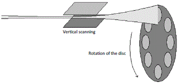
Such temperatures are prohibitive: photoresists, for example, can tolerate only moderated temperatures, of about 100°C. Beyond this level, they inflate, crackle or decompose. There is thus a compromise to be found between high output and reasonable heating. With a purely electrostatic scanning, the beam remains almost permanently on the same wafer that quickly heats up. On high current implanters, this way of proceeding is thus no longer possible. Thanks to a mechanical or mixed scanning, the power density is then distributed on all of the implantation batch, the beam periodically returning on the same sample only at each turn of the disc (see Figure 2.4).
Figure 2.3. Calculated values (full line) of the silicon temperature as a function of time and of the power density (irradiance). The curves in dotted lines correspond to the iso-dose contours reached under these conditions. According to [BRU 79]
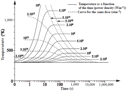
Figure 2.4. Example of mixed scanning of the beam on a high current implanter: the vertical scanning is electrostatic and the disc rotation ensures the ions distribution in the horizontal direction
However, for beam currents higher than 1 mA, these solutions are not sufficient and it is necessary to evacuate the calories by cooling the back face of the wafers. For that, there are two solutions: to directly cool with the help of a fluid (generally a gas) or indirectly, by thermal conductivity towards the sample holder, while trying to improve the contact.
Ion implantation in the semiconductor industry often implies insulating structures. A significant charge effect can be induced there by ions, causing a progressive deterioration of the dielectric qualities of the oxides, going, possibly, up to a disastrous breakdown. In addition, this charge effect can also disturb the behavior of the ions up to the target, producing a divergence of the beam. These problems are all the more severe, as the currents become more important. It is then necessary to maintain the target neutrality. This is generally carried out with the help of a “shower” of secondary electrons (therefore, of low energy) placed near the target, like, for example, the one in Figure 2.5.
Figure 2.5. Example of an “electronic shower” device intended to neutralize the charge induced in the target by positive ions
2.3. Ion range
2.3.1. Binary collision and stopping power
The slowing down of the ions in the material is characterized by the stopping power, noted (dE/dx), corresponding to the quantity of energy dE lost per elemental distance dx. It is a function of the energy E. The interaction between the projectile and a target atom is described by assuming two distinct processes: the collision between the two nucleui and the interactions with the electrons. The first corresponds to the Coulomb repulsion, causing an important deviation of the trajectory. The second is related to excitations and ionizations, leading to significant energy loss for the ion, but which do not alter its direction. The stopping power can thus be separated into two components: nuclear (dE/dx)n and electronics (dE/dx)e:
[2.2]![]()
The stopping cross-sections for each type of interaction, Sn and Se, are physical quantities independent of the density of the slowing environment, N is the atomic density.
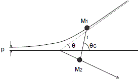
In the context of classical mechanics, the elastic binary collision with an atom of the target initially immobile, following the laws of conservation of energy and of momentum, we can write the energy transfer T as:
[2.3]![]()
where M1 and M2 are respectively masses of the ion and of the target atom. E is the energy and θC the scattering angle in the system of the center of mass (see Figure 2.6).
Figure 2.6. Diagram of the collision between the projectile (M1) and the target atom (M2)
The scattering angle is related to the interaction potential V(r) by the relation:
[2.4]
where p is the impact parameter (see Figure 2.6) and EC is the energy in the system of the center of mass (Ec=EM2/(M1+M2)). rmin is the collision radius between the two partners.
The potential used at implantation energies is of the Coulomb type, moderated by the shielding effect of the electrons. It is written:
[2.5]![]()
where Z1 and Z2 are the atomic numbers of the projectile and of the target, and ϕ is the shielding function, tending to 1 when r decreases. a is the shield radius estimated by Bohr [BOH 48], from the Thomas-Fermi atomic model:
[2.6]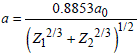
a0 is the Bohr radius (5.29.10-11m).
The cross-section (i.e. the probability that a collision, leading to the deflection 0C, occurs) is:
[2.7]![]()
And finally, the stopping cross-section is:
[2.8]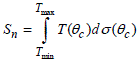
Tmax is given by equation [2.2] with θc=180°. Tmin is more difficult to define. It is of the order of magnitude of the displacement energy of the target atoms. To integrate this equation, Lindhard, Scharf and Schiott [LIN 63] introduce reduced variables, ε and ρ respectively proportional to the energy and to the ion range R:
[2.9]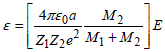
[2.10]![]()
By using these notations, the reduced stopping power of Lindhard, Scharf and Schiott (LSS) is connected to the actual stopping power by:
[2.11]![]()
Many works compare the merits of such or such a shielding function [WIL 77, ZIE 85a]. In the traditional implantation domain (ε<30), the nuclear stopping cross-section takes the following universal analytical form [ZIE 92]:
[2.12]![]()
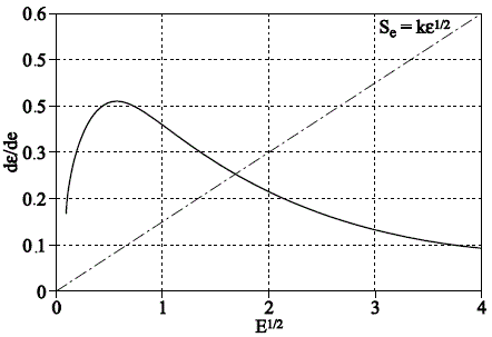
The nuclear stopping power dominates at very low speed. At higher energies, the electronic stopping power takes increasing importance and, always in the domain of implantation, its value is proportional to the speed:
[2.13]![]()
k is a constant without dimension, which depends on M1, M2, Z1, Z2. Thus, in opposition to the case of the nuclear stopping power, the electronic deceleration cannot be represented in the form of a universal curve. Nevertheless, for common projectiles, k varies between 0.1 and 0.2 (from the heaviest to the lightest) and, in the domain of interest, the stopping powers depend on the energy, as indicated in Figure 2.7. In this figure, the electronic stopping power is represented for k = 0.15.
The nuclear stopping power is at maximum at ε≈ 0.35, which corresponds to 3 keV for boron, 15 keV for phosphorus or 70 keV for arsenic in silicon. The electronic stopping power becomes dominant at ε> 2 for the lightest ions, and at ε> 4, for the heaviest, which, always in silicon, corresponds to 20 keV for boron, 140 keV for phosphorus or 800 keV for arsenic.
Figure 2.7. Stopping power cross-sections as a function of the square root of energy in LSS units [FLAX 63]
2.3.2. Profile of the implanted ions
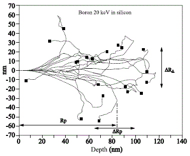
The total distance covered by an ion along its trajectory is called the range (noted R), but what interests the user is the distance covered in the normal direction to the target, which we call the projected range. The slowing down process being essentially statistical, the relevant parameters are the average projected range (noted RP) and the scattering of the values around RP, characterized by a longitudinal standard deviation ΔRP and a transverse standard deviation ΔR⊥ (see Figure 2.8).
To calculate these magnitudes, the concepts related to the binary collision and to the stopping powers are applied to the statistical problem of a series of collisions. For that, there are two solutions: the resolution of a transport equation [LIN 63] and the Monte Carlo approach [ROB 63]. The transport equation is written for the function probability density f(R, E) for an ion to have a range comprised between R and R +dR:
[2.14]![]()
This equation cannot be solved in this form. It is possible to develop f in moments fn, to rewrite the equation for the fn moment and to solve it. By definition, f1=Rp is the moment of order 1:
[2.15]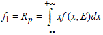
and ΔRp is related to the moment of order 2 by the relation:
[2.16]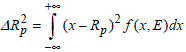
Figure 2.8. Range of about 20 boron ions of 20 keV in silicon (the trajectories are represented by a dotted line and the stopped boron by a black square) and definitions of the average projected range and of the longitudinal and transverse scatterings
The Monte Carlo calculation simulates the entire history of the projectile, collision after collision [BIE 80]. The final statistical assessment is carried out by summing and/or averaging on a large number of simulated trajectories. The position, direction and energy of the ion are the input data. The distance between two collisions, the impact parameter and the azimuth of each collision are the random variables. The elastic collisions deflect the trajectory. Between each collision, the ion loses energy proportionally to the electronic stopping power at the value of its instantaneous energy. The story stops when the energy of the ion drops under a certain value or when the ion leaves the target. The advantage of the Monte Carlo method compared to the transport equation relies on the 3D character of the reconstitution of the trajectories. The disadvantage is the calculation slowness.
The two methods give similar results, namely Rp and ΔRp. As a first approximation, we can then describe the profile of the implanted atoms as a Gaussian function:
[2.17]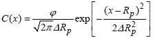
By comparing to the experimentally measured distributions, it is clear that, except when M1 = M2, the Gaussian approximation is not satisfactory. From the moments of order 3 and 4 of the function f(x, E), we define two dimensionless parameters, γ and β, respectively describing the profile asymmetry (skewness 2) and the sharp or squashed character of the maximum concentration peak (kurtosis):
[2.18]
[2.19]
There are various forms of distributions to rebuild the profiles from the first four moments [SEL 84]. The most usual one, regarding implantation in silicon, is the Pearson IV distribution:
[2.20]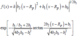
where k is a constant obtained thanks to the normalization condition:
[2.21]
The constants b0, b1, b2 are related to the four moments by:
[2.22]![]()
![]()
The maximum of a Pearson IV distribution is at x = Rp+b1. If γ < 0, the peak is beyond RP and the concentration is more important towards the surface than towards the depth. This is the case for light projectiles in a heavy target, for example boron in silicon (see Figure 2.9.). The situation is reversed for γ > 0. We find this shape for a heavy projectile in a light target, such as arsenic in silicon (see Figure 2.10.). γ = 0 and β = 3 correspond to a Gaussian distribution.
Figure 2.9. SRIM simulation [ZIE 85a] of the profile of boron atoms (50 keV 1015/cm2) implanted in silicon
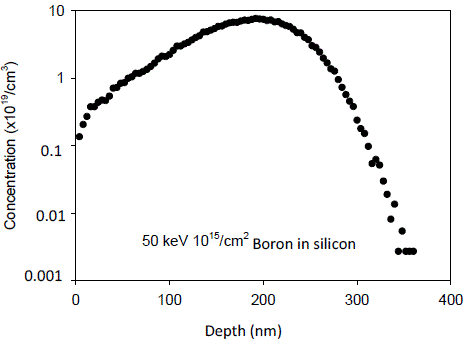
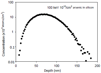
Figure 2.10. SRIM simulation [ZIE 85a] of the profile of arsenic atoms (100 keV 1015/cm2) implanted in silicon
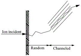
2.3.3. Backscattering, surface sputter and channeling
A certain number of phenomena can alter the shape of the concentration profile of implanted atoms. They appear under some specific conditions and are generally not taken into account in simulators.
Backscattering corresponds to the events of almost head-on collisions during which an energy close to Tmax=γE is transferred to the recoil atom, which can lead, if M1<M2, to a reflection of the projectile on the target surface. The backscattering coefficient, i.e. the number of reflected ions divided by the total number of projectiles can go up to 30% for low energy boron ions into silicon. This phenomenon must thus be taken into account to estimate the dose actually received by the target.
Sputtering corresponds to the ejection of surface atoms of the target under the action of elastic energy transfers. It is characterized by a sputtering coefficient S, corresponding to the number of atoms ejected per incident ion3. It is a function of M1, M2 and E. S reaches its strongest value at the energy corresponding to the maximum of nuclear stopping power. In silicon, it is then of the order of 5 for an antimony beam, of 3 for arsenic, of 1.5 for phosphorus and lower than 1 for boron.
The thickness of eroded material xs is related to S and to the dose ϕ by:
[2.23]![]()
By assuming that the sputtering rate remains constant during implantation, and that the profile is Gaussian, for high-dose implantation, the distribution will obey:
[2.24]
and with saturation (ϕ→∞), we will have:
[2.25]![]()
with a maximal concentration located at the surface, given by:
[2.26]
For high implantation doses, the profiles will evolve as shown in Figure 2.11. The surface sputtering is thus the only phenomenon actually limiting the quantity of atoms that we can introduce into a material by implantation4.
The critical angle ψC is very simply calculated, by writing the channeling condition, namely that the transverse kinetic energy of the ion remains lower than the repellent potential of the lattice row or plan.
This condition, for a crystalline axis, leads to the relation [LIN 65]:
[2.27]![]()
Figure 2.11. TRIDYN simulation [MOL 84] of the profile of antimony ions of 100 keV implanted in silicon at various doses
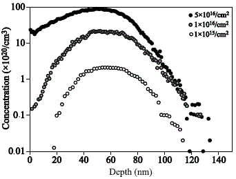
Figure 2.12. SIMS profiles of the boron implanted at 15 keV in silicon according to the incidence angle compared to the direction <100> of the crystal (according to [KLE 91])
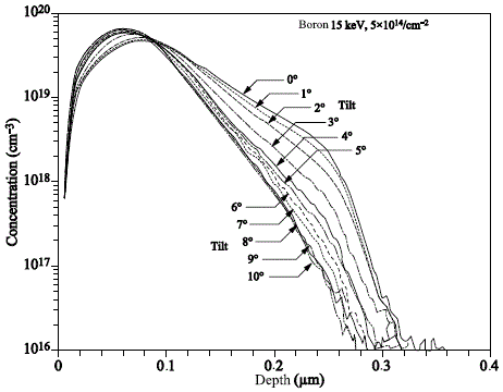
The order of magnitude is of a few degrees for usual implantation energies in silicon. It is higher in axial channeling than in planar channeling. The latter constitutes a major limitation to the realization of surface junctions by boron implantation. The tails in distributions can obviously be reduced, thanks to an accurate control of the orientaion of the wafers as a function of the beam direction. But, even with these precautions, the angular divergence of the ions compared to their initial direction, after a certain number of collisions, quickly becomes very important. This means that a part of them will always end up adopting a trajectory focused along the axis or secondary planes of the crystal (see Figure 2.13). This phenomenon explains the persistence of a tail in the distributions of Figure 2.12, even for incidence directions far from any channeling axis. The only way to completely remove this effect consists of destroying the crystalline order by pre-amorphizing the target.
Figure 2.13. Schematic representation of the ion channeling at the end of the course
2.3.4. Implantation through a mask
In the fabrication technology of electronic circuits, the implantations are almost always carried out through a mask containing openings, corresponding to zones to dope, and protected zones, where ions must be completely stopped. Resists, oxide layers (SiO2) or silicon nitride (Si3N4) are used to stop the projectiles. Because of their nature and their thickness d, the efficiency of these films is characterized by the transmission coefficient τ, i.e. the number of ions managing to cross, normalized to the total number of incident ions. By admitting a Gaussian distribution of the atoms stopped in the mask, an approximation formula of the transmission coefficient is:
[2.28]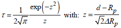
For example, if the user desires less than one projectile out of 104 to cross the layer, it is necessary that d is of about or higher than Rp+4ΔRp, Rp and ΔRp being the projected range and the standard deviation of the projectiles in the masking material.
Another important technological parameter is the form of the doping profile in the opening, and in particular the horizontal spread of the distributions at the edge of the mask. This spreading, caused by multiple collisions, is often as important as ΔRp. In the ideal case of an opening at the abrupt edges of 2l width, the distribution in 2D is obtained by multiplying in-depth the profile C(x) by the term:
[2.29]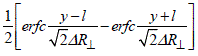
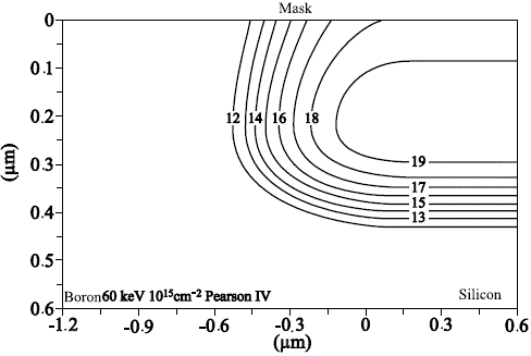
Figure 2.14 shows the contours of equal concentration (from 1019 to 1012cm-3) for boron ions of 60 keV, implanted at the dose of 1015 cm-2 through a mask with 1µm width. We can note that the doping can extend a few hundred nanometers and risk to interfer with the neighboring device, if the latter is set too close. The horizontal spread is thus a serious limitation to the integration of a growing number of devices per unit of silicon surface.
Figure 2.14. 2D profile calculated in the case of a vertical mask edge [SEL 84]
2.4. Creation and healing of the defects
2.4.1. Primary collision and cascade
When an ion of energy E comes to strike an atom of the target, the transferred energy is T (see relation [2.3]). If T is higher than a threshold energy Ed, called the displacement energy (of several eV), the recoil atom thus released will be able in its turn to cover a certain distance in the target, losing its energy through nuclear and electronic collisions. Repeating this, a series of atomic displacements is created, called a cascade. This lasts until the remaining energy in each individual cascade, and in particular the one of the primary ion, is lower than Ed. The entire duration of the cascade is very short: less than one picosecond.
In addition, transfers under the threshold often represent a significant part of the energy transfered to the slowing-down environment. They sometimes constitute the majority of events, resulting in an important creation of phonons, i.e. thermal oscillations, and thus finally in a local temperature rise. This thermalization proceeds on a time scale definitely longer than the cascade duration, of about one nanosecond. In a very simple model, Kinchin and Pease [KIN 55] estimate that at each collision, the average transferred energy is divided by two and thus, at the nth collision, the average transferred energy is T/2n. Finally, this model leads to a number of displaced atoms (per unit of target surface), proportional to the dose and to the total energy quantity v lost in elastic collisions:
[2.30]![]()
with:
[2.31]![]()
ν and η are thus respectively the total energy quantities lost in elastic collisions and electronic interactions.
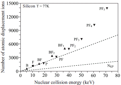
However, in practice, we notice (see Figure 2.15) that the number of created defects (here in silicon at low-temperature) is often much higher than predicted by the Kinchin-Pease (KP) model. The order of magnitude is a few hundred atoms moved by incident ion for a light projectile, a few thousand for a medium mass and several tens of thousands for a heavy projectile. At higher energy, the curves again take the linear slope of the KP relation, indicating that the creation of damage at high-energy obeys this law. At low energy, the important creation of defects is due to an effect related to the high density of transferred energy, leading to the overlay of the cascades initiated by the recoil atoms. This is equivalent to a collapse of the displacement energy. This phenomenon is usually called a displacement spike.
Figure 2.15. Total number of silicon atoms moved by incident ion, according to the total quantity of energy lost in elastic collisions (according to [WAL 78]). The dashed line corresponds to the standard Kinchin and Pease model (relation [2.30])
This phenomenon of cascade overlay is obviously even more important during the implantation of polyatomic ions, such as BF2+ or decaborane, commonly used in microelectronic technology. Figure 2.16 shows how the number of displaced silicon atoms gradually deviates from the linear behavior, depending on the number of atoms contained in the molecule [GRO 87].
For an in-depth calculation of the distribution of displaced atoms in a linear cascade, the two methods described in section 2.3 (the transport equation or the Monte Carlo calculation) are used. The transport equation [SIG 72] is written in a general way for the defect distribution function ![]() which is the amount of deposited power (in nuclear or electronic collisions) in the element of volume (r, d3r):
which is the amount of deposited power (in nuclear or electronic collisions) in the element of volume (r, d3r):
[2.32]![]()
where v is the initial speed before the collision of probability dσ, v’ is the speed of the ion after scattering and v” is the speed of the recoil atom.
Obviously, the standardization condition is:
- for elastic collisions:
[2.33a]![]()
- for electronic collisions:
[2.33b]![]()
Figure 2.16. Number of silicon atoms moved at 77 K (measured by RBS-C in situ) by the implantation of various polyatomic projectiles, according to the energy lost in elastic collisions. This number grows quicker than linearly (dshed line) and it is much more important than the Kinchin and Pease standard model predicting it (dotted line) (according to [GRO 87])
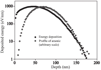
With TRIM or SRIM [ZIE 85a], after the reconstitution of a number n of trajectories, we can obtain the profile of energy deposition, i.e. the Fd function, in the two categories of interaction. Figure 2.17 shows the profile of energy deposition in elastic collisions, for 100 keV arsenic in silicon, compared to the distribution of the implanted ions. These profiles do not coincide: a maximum of energy is deposited before the ions stopping. The defects (see the following section) are created according to the profile of energy deposition.
If Fd (x = 0) is the energy lost in elastic collisions at the surface of the target, we can then estimate the surface sputter rate S:
[2.34]![]()
where Eds is the energy of surface displacement (close to the sublimation energy) and Λ = 0.042 Å-2 [SIG 72].
Figure 2.17. Comparison between the profile of the deposited energy in elastic collisions (black dots and left scale) and distribution of the arsenic implanted (white dots and arbitrary scale) at 100 keV in silicon (SRIM simulation)
2.4.2. Point defects
A solid is always constituted of a more or less ordered atom assembly. The concept of point defect is thus relatively easy to define, especially in the microelectronics materials, which are often perfect single crystals. Elementary point defects are thus the vacancies, i.e. vacant sites in the network, and the interstitials, which are supernumerary atoms located between the atoms of the network. After implantation, the interstitial species are the implanted atoms, but also the atoms moved from the target, called self-interstitials. Several configurations are possible for these interstitials, all of them allowing the atom to be inserted in the network. Moreover, around the vacancy, as well as around the interstitial, a local rearrangement is necessary. In silicon, we estimate that the defects’ formation energy, corresponding to the difference of the free enthalpies, before and after their formation, is about 1 eV for a vacancy and 3 to 5 eV for an interstitial.
An energy transfer higher than the displacement threshold produces a Frenkel pair (vacancy + interstitial). The simple addition of the formation enthalpies makes it possible to estimate those of a Frenkel pair in silicon at approximately 4 to 6 eV. To that, we must add the energy we had to spend to break the Si-Si bonds. Moreover, if the separation distance between the two components of the Frenkel pair is not sufficient, the thermal diffusion process and sometimes the electrostatic attraction will cause their recombination. We thus need a little more important energy transfer, so that the interstitial can cover a certain distance separating it sufficiently from the vacancy. In other words, the threshold formation energy of a stable Frenkel pair is rather about 10 to 80 eV (respectively from gallium arsenide to diamond). It is of 15 eV in silicon.
It is quite obvious that, beyond this little simplistic classification in vacancies and interstitials, the defects also differ by their configuration and by the connections made in their environment, including possible hybridizations of the target atoms or of impurities. For example, an interstitial often takes a configuration of shared site with an atom of the material, in energetically favorable crystallographic directions such as <100> or <110>. This is particularly true in ionic-covalent crystals, where there is an important lattice—electron interaction, which often produces important relaxation effects around a defect.
We said that the first stage, the cascade, occurs in approximately 10-13 seconds, and the second one, thermalization, in 10-9 s. The rearrangement described above is the third stage, bringing the system towards a new equilibrium. It occurs on a much longer period of time. In the second stage and especially in the third stage, events such as diffusion, precipitation or chemical reactions can occur. We then understand that other defects can be formed. They are more complex and considered as point defects, but are already defect combinations: for example the double or triple vacancy, etc., the vacancy-impurity pairs and, in covalent compounds, the antisite defects.
2.4.3. Accumulation of damages, amorphization
During implantation, elementary defects (interstitial and vacancies) are generated proportionally to the projectiles’ flux. They can recombine and/or destroy themselves on “sinks” (grain boundary, surfaces, interfaces, dislocations, etc.) or diffuse, proportionally to their local gradient. Without writing too complex equations, two extreme situations can arise:
— the generation rate (i.e. the projectile flux or mass) is low and/or the diffusion is important. The creation of Frenkel pairs is permanently compensated by re-combinations and annihilations. We thus reach a stationary state, with a low concentration of vacancies and isolated interstitials. This is the case during a high temperature implantation or with light ions;
— the ion flux is important (this is the case, as we saw, with modern implanters) and/or the diffusion is low, so that the generation rate of the Frenkel pairs is more important than the re-combinations or the other forms of elimination of point defects. These pairs will thus accumulate proportionally with the in-depth profile of the energy deposition, leading first to the formation of small defects aggregates, and then finally of real amorphous zones. If nd(x) is the number of atoms moved at the depth x, we can, as a first approximation, say that a(x) = nd/N is the “amorphous” fraction at this same depth. The increase (da) in the amorphization for a dose increase (dϕ) will be proportional to the remaining crystalline fraction (1–a), to the value of the local energy deposition Fd(x) and inversely proportional to the displacement energy:
[2.35]![]()
So that:
[2.36]![]()
At low doses, we find that the defects creation is directly proportional to the energy deposited in elastic collisions:
[2.37]![]()
This simple model describes, rather well, the accumulation of damage in most materials, without self-healing, i.e. at low temperature. In reality, we note that it becomes increasingly easier to move atoms in an already damaged material, so that the displacement cross-section Fd/NEd varies itself with the dose. Assuming a linear variation, we find:
[2.38]![]()
The solution of this equation is:
[2.39]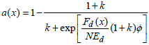
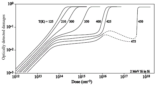
This sigmoidal variation law describes the amorphization of silicon for usual implantation energies at ordinary temperature rather well. More complex models have been proposed [WEB 00]. Lastly, let us note that above a critical damage density, corresponding to a critical dose ϕc, the crystal cohesion is no longer ensured and the material collapses very quickly towards the amorphous phase. This critical density is about 10 to 20% in silicon. Moreover, as previously discussed, this law of damage accumulation is valid as long as the re-combinations, healings, migrations or other rearrangements of defects are not too important. In the opposite case (at high temperature), the Frenkel pairs’ generation is largely counterbalanced by recombinations. We thus reach a stationary state, which will never lead to the material amorphization. At intermediate situations, the critical amorphization dose backs down, as the implantation temperature increases (it also depends, of course, on the projectile mass). All these behaviors are evidenced on the experimental curve in Figure 2.18, describing silicon damaging by high-energy silicon ions (linear cascades) [HEC 89].
Figure 2.18. Silicon fraction damaged by Si ions of 2 MeV as a function of the implantation dose and temperature [HEC 89]
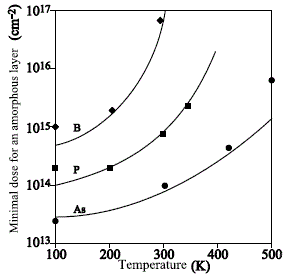
Using an amorphization model based on similar mechanisms, Morehead and Crowder [MOR 70] determined, for various projectiles, the critical dose for silicon amorphization as a function of the implantation temperature (see Figure 2.19).
Figure 2.19. Necessary critical dose to form an amorphous layer in silicon at various temperatures and using various projectiles [MOR 70]
Therefore, including the temperature influence, it is better to write (for low doses):
[2.40]![]()
where ξ(T) accounts for the efficiency of defect creation, the net result of the creation-healing process. By integrating nd(x) on all the implanted thickness, we obtain a relation similar to the Kinchin and Pease relation [2.30], giving the total amount Nd of displaced atoms proportional to the amount v of power lost in elastic collisions. With the critical amorphization dose, the product ξ(T)Fd(x)ϕc/N represents a critical energy deposition per atom, at the temperature T. At ordinary temperature, in silicon, this critical deposition is about 10 to 12 eV/atom [VIE 87]. For example, boron, at the doses usually used in microelectronics, does not reach this threshold and will thus not amorphize silicon at ambient temperature.
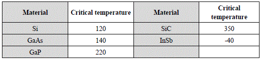
However, even at ordinary temperature, point defects (vacancies and interstitials) are very mobile. Behaviors other than the simple accumulation in the form of amorphous agglomerates will thus appear: first of all the already quoted recombination, equivalent to a self-healing of the damages; the combination, also already mentioned, of interstitials and vacancies, between them or with impurities; the clustering of the vacancies and interstitials in a more ordered form, which leads, especially when the temperature is raised, to the formation of extended defects (for example dislocation loops5). A simple calculation shows, for example, that above a certain number of atoms, the insertion of a loop in the silicon lattice is less expensive in energy than the insertion of an amorphous sphere. Obviously, the transition from one to the other also requires a certain energy, which can be provided, for example, by a rise in temperature during or after the implantation (see section 2.4.4 – Damage healing). In practice, in the absence of nonlinear effects such as displacement spikes, there is thus a critical transition temperature below which the displaced atoms will evolve towards the amorphous phase, and above which extended defects will be formed, for example, in silicon, {311}6 defects or interstitial loops. Table 2.1 gives the value of this temperature in some common semiconductors.
Table 2.1. Critical temperature (in °C) beyond which it becomes impossible to amorphize some common semiconductors
2.4.4. Damage healing and dopant activation
The aim of the implantation method in semiconductors is to set the dopants in substitutional position, where they are electrically active. The first condition is thus to restore the initial crystalline order. This recrystallization occurs during a thermal process (annealing). The conditions of this annealing will ideally be selected, so that the dopants can be positioned at the same time in substitutional sites. The first condition is related to the morphology of the damaged area, according to whether it is amorphized or not. In the first case, it is the recrystallization front (the amorphous-crystal interface), which, by passing through the implanted area, will cause dopant activation. In the second case, there is no epitaxy front. The dopant itself will have to diffuse to the vacant sites. Figure 2.20 illustrates these two situations with the active phosphorus fraction in silicon, depending on the implantation temperature.
Figure 2.20. Variations of the carriers concentration with the annealing temperature in silicon implanted with phosphorus at various temperatures (according to [TAM 71])
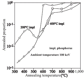
At ambient temperature, i.e. below the critical temperature reported in Table 2.1, an almost total phosphorus activation is reached with the annealing at 600°C. Above this value (implantations at 200 or 600°C in this example), the full dopant activation requires a much higher annealing temperature. Moreover, for annealing between 300 and 600°C, the activity increases and then decreases again. This effect of reverse annealing is well-known in the case of boron implantations which, at traditional microelectronics doses, do not amorphize silicon at room temperature. It is related to the formation, then to the dissolution, of the intermediate extended {311} defects [SEI 71]. Beyond this temperature range, the setting in substitution of the dopants is controlled by a process, the activation energy of which is about 5 eV. The common interpretation assigns this value to the generation and the migration of silicon vacancies, which, while reacting with boron or interstitial phosphorus, lead to the full activation [HOF 75].
A very different situation arises when the implanted layer is amorphized. Indeed, the latter recrystallizes at rather low temperatures (approximately 500°C in silicon) by solid phase epitaxy (SPE), from the underlying crystalline substrate [CSE 78]. The amorphous-crystal interface moves towards the surface with a constant speed vEPS given by:
[2.41]![]()
with an activation energy of 2.68 eV, measured up to 1,300°C in silicon [OLS 88] and of 1.55 eV in InP or AsGa [LIC 91]. v0 depends on the crystal orientation and on the presence of impurities. The most favorable orientation is <100> and v0 is the lowest for the <111> orientation. [CSE 76]. A high dopant concentration increases the epitaxy rate, by a factor of 2 or 3 for approximately 1020 cm-3 of phosphorus for example. An equivalent oxygen concentration slows down the recrystallization in the same proportions [LAU 80]. However, all impurities, even the dopants, as soon as their concentration exceeds the solubility limit, slow down the epitaxy and, thus, low concentrations of not very soluble impurities can potentially completely inhibit it, leading then to the formation of a polycrystalline phase. The same mechanisms intervene in other semiconductor materials, more or less shifted in the temperatures scale: for example the typical temperature of recrystallization of germanium is 300°C, and that of SiC is about 1,500°C.
Figure 2.21. Images of transmission electron microscopy (plane view) of the “end of range” defects formed in amorphized silicon (Ge 150 keV, 2×10¹⁵/cm2) and annealed at 1,000°C for increasing times (10, 50,100,200 and 400 s) [BON 96]
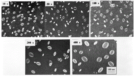
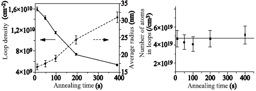
Some residual defects remain after the solid phase epitaxy of an amorphous layer. They result from the presence, beyond the original amorphous-crystal interface, of an excess of recoil self-interstitials, compared to the local concentration of vacancies. In silicon, during annealing, a significant part of them will condense in {311} defects in the temperature range 600–750°C or in dislocation loops in the range 800–1 100°C. These defects are called EOR (end of range defects). They are set in the (111) planes. The series of photomicrographs in Figure 2.21 show the morphology and development in size and population of these defects during an annealing at 1,000°C. In fact, the {311} are intermediate defects dissolving in their turn for more important thermal budgets, releasing thus interstitials, which then evolve towards loops. They are not really healing any more, since recent studies [BON 96], [CLA 95] have shown that loops obey a conservative competitive growth mechanism (see Figure 2.22). Their radius increases, while their density decreases, but the total number of interstitials included in the loops is constant. However, the proximity of the surface can modify the conservative character of this equilibrium.
Figure 2.22. Left: development during the annealing time (at 1,000°C) of the density and of the average radius of EOR defects observed in Figure 2.21. Right: development of the total number of atoms (per cm2) taken in the loops functions of the annealing time at 1,000°C [BON 96]
These defects can be traps for impurities or for charge carriers, altering the electric behavior of the devices. Moreover, excess interstitials can also, transitorily, take part in the diffusion of the dopants located in this zone. Generally, since the dopants diffuse in semiconductors via mechanisms assisted by vacancies and/or self-interstitials, any local and/or temporal supersaturation (or undersaturation) of one or the others, created by implantation, will cause an “abnormal” diffusion. This aspect of implantation is sometimes used to adjust a doping profile, in particular to slow down diffusion [NIS 92].
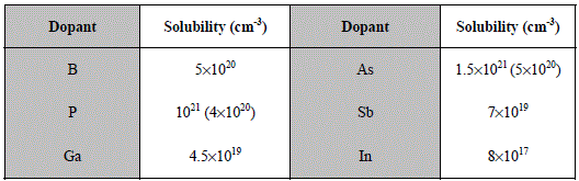
Regarding dopant activation, we need to recall that the quantity of impurities that can be set in substitutional sites is limited. Beyond this limit, they precipitate in the form of immobile (in terms of diffusion) and inactive (from an electric point of view) clusters. However, for some dopants, such as arsenic or phosphorus in silicon, there is an “absolute” solubility limit and another one concerning their electrical activity. This characteristic is due to the fact that these elements, implanted at high-dose and placed in substitution during annealing, have a high probability of finding another identical atom (or several) as first (or second) neighbors in the crystal. This modifies their energy level in the band gap, and thus their probability of ionization. Table 2.2 gives the maximum solubility value (at high temperature) of the main silicon dopants. Except at high temperature, where it saturates and sometimes decreases, solubility is the result of a thermal activated process. It is thus much lower at low-temperatures and the dopants can thus precipitate during annealing at these temperatures. The forced recrystallization around these precipitates also leads to the formation of dislocations. However, the fast motion of an solid phase epitaxy front through the dopants profile can result in largely exceeding the solubility values and thus in incorporating, in a metastable state, a large amount of impurities [NAR 82].
Table 2.2. Maximum value of the solubility of various dopants in silicon. The value between brackets is the solubility of the electrically active atoms
2.5. Applications in traditional technologies and new tendencies
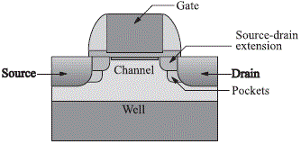
The implantation is used in most doping operations of MOS and bipolar technologies. We will describe the common operations in these sectors and the new tendencies constituting advances towards new technological lines [HIL 91, KUS 91]. The first are schematized in Figure 2.23, in the case of CMOS technology:
— doping of the p- and n-wells;
— adjustment of the threshold voltage by a light over doping of the channel under the gate oxide;
— doping of the source and drain extensions (LDD);
— pockets or “anti-punch through” halos;
— source and drain doping;
— gate polycrystalline silicon doping.
Figure 2.23. Areas implanted in traditional CMOS technology
2.5.1. Common implantations
The N- or P-MOS transistors are placed in “wells” of opposite type in order to form a junction insulating the transistor. The surface concentration in this well, just like the nature of the gate electrode or the oxide thickness, affects the threshold voltage at which the device lets the current pass. It also conditions the importance of the leakage currents between neighboring circuits. The doping precision, necessary for well, makes the implantation essential in this case. Typically, p and n doping are respectively carried out with boron and phosphorus ions, with energies in the 100 – 200 keV range and doses between 1012 and 1013 cm-2. These implantations are followed by a long annealing at high temperature, in order to form a deep junction. The tendency in this sector is to replace these diffusions with high thermal budget by deep implantations, therefore at higher energy. This also has the advantage of forming a “retrograde” doping profile, advantageous to decrease the gain of parasitic transistors.
The threshold voltage to which the channel of the MOS transistor starts to conduct is a parameter with a strong importance. The adjustment of this voltage, in the n and p parts of the transistor, is carried out by introducing a small quantity of boron or phosphorus (about 1011 cm-2) right under the gate oxide. The energy and dose are selected according to the thickness of this oxide.
The performances of the submicron transistors depend on the impurity profile close to the drains. A gradual profile, called LDD (lightly doped drain) can reduce the electric field in this zone and thus avoid the injection of “hot” electrons, which could deteriorate the N-transistor. The effect also exists, but in lower proportions, for the holes in the P-transistor. This doping of the channel-drain transition zone is carried out by a self-aligned implantation, possibly at an oblique incidence (up to 60 degrees) of phosphorus or arsenic (for n-type dopant) and boron (for p-doping). Doses are about several 1013 ions/cm2 (see Figure 2.24).
Figure 2.24. Schematic representation of the realization of LDD and anti-“punch through” doping
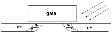
In this same zone, when the channel is very short, the transistor behavior can be alter by the “punch through” effect, if, under functioning (under polarization), the depletion zone of the drain-channel junction reaches the source-channel junction. This punch through effect is avoided by a phosphorus or boron implantation, possibly again in oblique incidence, with doses of about several 1012 ions/cm2, right under the active channel, in the area adjacent to the drain and source. Accurate control of the zone to be doped requires slightly higher energies: about 100 keV for boron and 150 keV for phosphorus (see Figure 2.24).
An implantation, not mentioned in Figure 2.23, relates to the recent lateral insulation technology by the formation of trenches (shallow trench isolation STI). An over-doping, at the bottom of the trench and close to the walls can be carried out by boron implantation (typically 100 keV, 1013/cm2), by varying the incidence angle by a few degrees around the trench axis.
The “source” and “drain” zones are doped at high concentrations, about 1020 to 1021/cm3, with the opposite type of the channel zone, itself doped at 1016 or 1017/cm3. With the common circuit dimensions, these junctions must be very thin.
Arsenic (a heavy ion) is thus preferred to phosphorus, to build the n-junction. Boron being the only p-type dopant sufficiently soluble to reach the required level of concentration, there is hardly any choice but to implant it at very low energy (several keV) or to implant the BF2+ molecule. The doses are about 5×10¹⁵/cm2. We will discuss further the prospects regarding the realization of even more superficial junctions.
The gate electrode of the CMOS transistors, for both the N- and P-type, is formed by a pattern of deposited polycrystalline silicon. But this material, in its as-deposited form, is too resistive. It must thus be doped to increase its conductivity. This doping can possibly be made through chemistry during the deposition step, but, more often, the Si-poly is doped by arsenic or BF2+ implantation, with doses of about a few 1015 with 1016/cm2. This doping is often carried out at the same time as the doping of the source and drain.
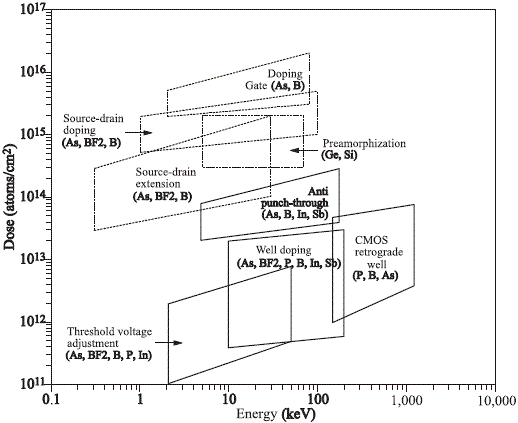
Figure 2.25 summarizes all these operations in the form of a dose-energy graph.
Figure 2.25. Domains of energies and doses corresponding to the various operations of doping or amorphization of silicon in CMOS technology
Implantation was also essential in bipolar technology when, for reasons of speed of the circuits and of more advanced integration, the need was felt to precisely control the vertical spacing between the emitter, the base and the collector. In this context, the parasitic “emitter push effect”7 should absolutely be avoided. This was achieved by using an arsenic implantation (several tens of keV, at doses higher than 1015/cm2) instead of a phosphorus diffusion.
There again, once installed in the technological lines, the implantation was spread to all the other doping steps: creation of the buried emitters (As, Sb, several tens of keV, >1015/cm2) and of the base (B, several keV, <1014/cm2), channel stop (B, 1013/cm2), contact doping, etc.
2.5.2. Other applications and new tendencies
2.5.2.1. Gettering
Metal contamination is a recurrent problem for the microelectronics industry. Even at very low concentration levels, it brings various harmful effects, in particular an increase in the leakage current of the reverse-biased junctions and a deterioration of the carriers lifetime. The most common impurities (Fe, Cr, Cu, Ni) diffuse very quickly and are relatively soluble at high temperature in the common semiconductors. Their introduction occurs in all the stages of the manufacturing process: growth, cleaning, etching, ion implantation and, naturally, high temperature thermal treatments (oxidation, diffusion, annealing). Gettering processes of these impurities are commonly used. They consist of attracting and maintaining these elements far from the active areas of the circuits. We often separates the trapping mechanisms into two categories: gettering by segregation, which consists of depositing or forming on the contaminated substrate a material in which the impurity is very soluble; and gettering by relaxation, which consists of causing precipitation at the desired location, using an annealing at a temperature lower than that of contamination. Gettering by ion implantation is part of the second category. Indeed, any site of heterogeneous nucleation is a gettering center and the implantation can thus be used to intentionally create these sites. In fact, most impurities and defects introduced by implantation are gettering centers: boron, which forms Fe-B complexes [KIM 83], carbon capturing self-interstitials [ROH 95, WON 89], helium forming cavities [MYE 96, ROQ 00], argon gathering in bubbles [GRO 96, ROH 95] or either dislocations [SUM 99], etc. It seems that the stability of the cavities formed after implantation and desorption of helium makes them the most efficient gettering traps in silicon. In addition, cavities also introduce levels near the center of the band gap. This offers the possibility to locally control the carrier lifetime. This method was applied to power devices [RAI 98, ROQ 00].
2.5.2.2. High energy implantation
In the manufacturing process of integrated circuits, very deeply implanted layers have some advantages, and offer new technological possibilities. First, a high energy implantation instead of a pre-deposition, followed by a long diffusion, considerably reduces the thermal budget. This also has the advantage of a significantly lower lateral spread of the doping. Moreover, the implantation doping profile, contrary to a diffusion profile, has a higher concentration in-depth than on the surface. This can be used for better control of the interactions between neighboring devices (latch-up) or to avoid the punch through effect due to the wells [ZAP 88]. More generally, a series of implantations at various energies and doses can be used to accurately adjust a doping profile with a very weak thermal budget [CAP 95].
In addition, high-energy implantation can also be used to prevent radiation effects, while forming a buried “gate”, whose role will be to reduce the spread of the depletion region of surface junctions. Thus, a reduced number of possible parasitic charges will be able to go up towards the active devices [ZIE 85b].
Lastly, a deep implantation is able to form gettering centers for metal impurities close to the active areas [CHE 89].
2.5.2.3. Ultra-thin junctions
The realization of very shallow P+/N junctions remains a crucial manufacturing step of the current and upcoming CMOS structures, in particular for the control of short channel effects. Reducing the transient enhanced diffusion (TED)8) of boron and achieving its full activation is a challenge, insofar as strong doping implies a high implantation dose and thus an important quantity of defects, which will favor the dopant migration.
Let us recall that boron diffuses in silicon mainly via a mechanism where self-interstitials play a predominant role. Regarding implantation, the first precaution is obviously to reduce ion penetration. There are two solutions to implement this precaution: either, in a traditional implanter, decrease their energy up to values lower than 1 keV [CRI 04, LAL 05] and/or implant polyatomic ions such as decaborane [MAT 97, SMI 98], or immerse the sample in a plasma containing the doping element [QIA 91, SKO 04, YAN 98]. On the other hand, as seen in section 2.3.3, it is important to abolish channeling tails by pre-amorphizing silicon, for example by the implantation of a moderate dose of silicon or germanium [MIN 94]. To activate the totality of boron, temperatures of about or higher than 900°C are necessary. In this temperature range, EOR dissolve by releasing interstitials, contributing to the boron diffusion. To minimize it, we can reduce the annealing duration, by using, for example, a rapid annealing (RTA), of about one second up to 1,000 or 1,100°C [CLA 95].
We can also try to trap these self-interstitials, for example by carbon or fluorine implantation [GRA 05, VAN 05]. Carbon forms with interstitials stable C-Si complexes [MIR 02].
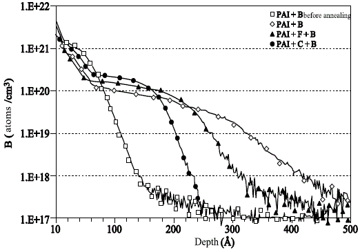
We can then note a decrease in the quantity of the formed EOR [CAC 96, CHE 99] and a significant reduction of the boron diffusion [GRA 05, PAW 06]. Figure 2.26 shows that by combining pre-amorphization, low energy boron implantation, fluorine or carbon implantation and rapid annealing, the doping can be maintained on a depth of about 20 or 30 nm [GRA 05].
Figure 2.26. Boron profiles obtained by boron implantation at 0.5 keV (1015/cm2) in pre-amorphized silicon (PAI), before (squares) and after rapid annealing at 1050°C, without (rhombuses) or with preliminary addition of fluorine (triangles) or carbon (circles) (according to [GRA 05])
2.5.2.4. SIMOX and Smart-Cut™
Silicon on insulator (SOI) substrate opened up a new branch of the silicon industry, because there are many possibilities for new applications, for sensors but also for low consumption and low voltage electronics. Electronic circuits on SOI [COL 04] have many advantages; most of them related to the fact that, on such a structure, devices are completely isolated from one another, as well as from the substrate. This results in reduced parasitic capacitances, in an almost total immunity towards the interactions between the neighboring circuits or towards the radiation effects and, generally, in the performance improvement of most of the active devices. However nowadays, there are hardly more than two industrially viable ways to prepare a SOI structure. They both use ion implantation: the SIMOX (separation by implantation of oxygen) technique and, more recently, the Smart-Cut™ method (developed by the French company, SOITEC).
The SIMOX technique [AUB 95, IZU 78] consists of synthesizing the SiO2 oxide by the implantation of a very high oxygen dose (about 1018/cm2) in silicon. The energy of oxygen ions must be sufficient (approximately 200 keV) to form a buried layer, leaving on the surface an intact silicon film. To preserve the single-crystal character of this film, the implantation is carried out at high temperature (about 600°C).
Lastly, to cause the growth and then the coalescence of SiO2 precipitates until the formation of a homogeneous layer with well-defined interfaces, an annealing of about one hour at very high temperature (≥1,300°C) is necessary. This is a very expensive technique, because of the very important dose, requiring a dedicated implanter (very high current) and because of the very high thermal budget. Moreover, implantation and annealing, under these conditions, require particular care, as for possible metal contaminations. Finally, the formed material often has a strong dislocations density.
The Smart-Cut™ method is done in four steps (see Figure 2.27) [BRU 95]. First, a hydrogen dose of about 1017/cm2 is implanted in a wafer (A) of oxidized silicon. The energy of H+ ions must be sufficient, so that they cross oxide and are implanted in silicon.
During the second stage, after cleaning, wafer A is pasted by molecular adhesion with a silicon wafer Bv (wafer bonding). Cleaning and polishing are crucial processes in this stage [MOR 96]. Then, a heat treatment is applied to the whole. Thank to the fact that wafer B acts as s stiffener and to the driving force linked to the gaseous pressure inside the cavities formed by hydrogen implantation (see Figure 2.28), stresses spread parallel with the surface, ending with the fracture occuringe at the maximum H concentration (see Figure 2.29).
The thin SiO2/Si film of wafer A is thus “transferred” on wafer B, which then has a SOI structure. The last stage is a polishing of the surface, which is relatively rough after the transfer.
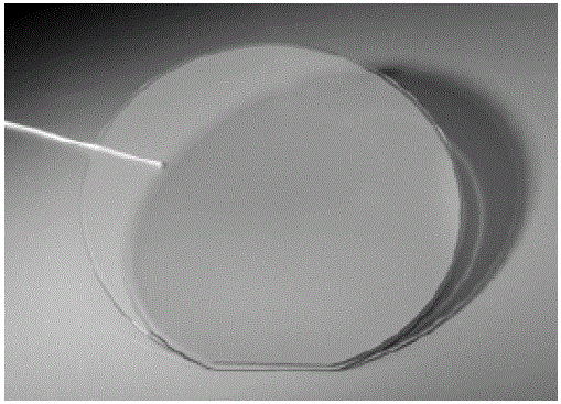
There are many advantages to this method. The most important are a low thermal budget and a limited damage, given the projectile mass. This results in an excellent material quality. Moreover, the method can be applied to the transfer of other materials, opening multiple possibilities for applications based on heterostructures (for example GaAs/Si) or on semiconductors on insulator (for example SiC/SiO2/Si) or even silicon on quartz (see Figure 2.30) [BRU 06].
Figure 2.27. The Smart-Cut™ method
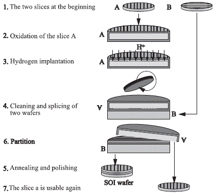
Figure 2.28. Transmission electron microscopy image (planar view) showing the coalescence of the blisters as a function of the annealing time [ASP 01]
Figure 2.29. Transmission electron microscopy image (transverse section) of a micro crack located around Rp [ASP 01]
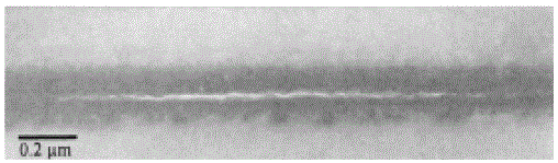
Figure 2.30. Silicon on quartz wafer
2.5.2.5. Towards nanoelectronics?
The recent development of nanotechnologies does not spare, obviously, the electronics domain. Current microelectronics is reaching its ultimate limits, regarding the reduction of the device dimensions. New approaches, involving nanoscale sizes objects, are seriously considered for the electronics of the future. The manufacturing methods of nano-objects are traditionally classified into three strategies: the first uses a very high-resolution lithography; the second consists of building these objects atom by atom, for example under the tip of a microscope with the tunnel effect; the third relies on mechanisms of a certain self-organization, concerning of course, a larger number of atoms. Ion implantation could be carried out with the first and third categories.
High-resolution lithography is indeed possible using a focused ion beam [HAR 91]. The current technology of focused beams uses sources with liquid metal (Ga), which have the characteristic of a virtual source point of very small dimensions. The object point can then be reduced to dimensions of about 15 nm, and lines 20 nm wide could be written in resist. It is thus a direct writing process (without mask), with a beam driving and/or a displacement of the target similar to electron beam lithography. However, the lateral energy deposition is, far less important, which makes it possible to reach these ultimate resolutions.
The activity concerning the surface self-organization is dominated by various growth methods (MBE, CVD). But volume self-organization (in other words the germination and the growth of an array of nano-precipitates) is governed by a certain number of non-equilibrium thermodynamics mechanisms, accessible, or at least adjustable, with the help of implantations and annealing, i.e. with tools available in the usual microelectronic technology. Nano-precipitates are organized according to the competitive growth process: the smallest are unstable and dissolve themselves during annealing for the benefit of the largest [PHI 85]. Depending on the local concentration, a so-called balance is established, forming precipitates of similar sizes, relatively regularly spaced from one another. Thanks to this phenomenon, nano-scale precipitates of all natures have already been synthesized in traditional microelectronics substrates, namely silicon and SiO2 oxide.
Two main tendencies are prominent in these studies, depending on the applications. In the first one, optoelectronics, we seek to use these semiconductor nano-crystals to carry out light emitting devices on a silicon-based substrate [CHE 08, GON 00, LUT 00] (the emission wavelength is a function of the nature and size of the object). The second one, in nano-electronics itself, the capacity of these nano-crystal to store and restore charges seems very promising [CAR 03, DUG 06, THE 00]. An identical approach is applied to the metal nano-particles: researchers, in both cases, attempt to connect their size and density to their electronic, optical or magnetic properties. Devices, able to control the electrons one by one, up to temperatures close to ambient temperature, were recently created, with a single contact plug, as well as networks of contact plugs, necessarily disordered, prepared by surface techniques [COR 98]. However, their characteristics are still not really reproducible nowadays. Similar devices could be made by implantation and annealing.
2.6. Conclusion
Ion implantation is an essential method of micro-electronics technology. Implanters are now common clean room instruments. They are entirely automated and highly reliable. The physicochemical mechanisms determining the doping profiles and the damage are known in detail. Few innovations are thus to be expected in the field of implantation applied to conventional technology. However, new needs appear, aiming, for example, at extending the energy field, to carry out surface junctions, as well as very deep wells, or even to reduce the doping thermal budget. It raises the problem of influence of residual defects, transitorily present, on the dopants diffusion. Moreover, new methods are proposed, which are less conventional than simple doping, such as proximity gettering or the realization of semiconductor structures on an insulator. In this field, a new branch of the silicon industry has been recently developed, thanks to hydrogen implantation and to the Smart-CutTM method. Finally, the arrival in force of nanotechnologies seems to open up new research tracks for ion implantation.
2.7. Bibliography
[ASP 01] ASPAR B. et al., “The generic nature of Smart Cut® process for thin film transfer”, Journal of Electronic Materials, vol. 30, no. 7, 2001.
[AUB 95] AUBERTON-HERVE A., WITTKOWER A., ASPAR B., “Characterization by atomic force microscopy of SDOI layer”, Nuclear Instrument and Methods in Physics Research, section B96, p. 420, 1995.
[BIE 80] BIERSACK J.P., HAGGMARK L., “The mean projected range and range straggling of Xe ions implanted”, Nuclear Instrument and Methods in Physics Research, vol. 174, p. 257, 1980.
[BOH 48] BOHR N., Matematisk-Fysiske Meddelelser – Danske Videnskabernes Selskab, Royal Danish Academy of Sciences and Letters XVIII, vol. 8, 1948.
[BON 96] BONAFOS C., Rôle des défauts end-of-range dans la diffusion anormale du bore, Thesis, Institut des sciences appliqués, Toulouse, October 1996.
[BRU 79] BRUEL M., BERTHET B., FLOCCARI M., MICHAUD J.F., Radiation Effects and Defects in Solids Incorporating Plasma Science and Plasma Technology, vol. 44, 173, 1979.
[BRU 95] BRUEL M., “Silicon on insulator material technology”, Electronics Letters, vol. 31, no. 14, p. 1201, 1995.
[BRU 06] BRUEL M., “16th International conference on ion implantation technology”, AIP Conference Proceedings, vol. 866, p. 76, Marseille, 2006.
[CAC 96] CACCIATO A.E., KLAPPE J.G., COWERN N.E.B., VANDERVOST W., BIRO L.P., CUSTER J.S., SARIS F.W., “Dislocation formation and B transient diffusion in C co-implanted Si”, Journal of Applied Physics, vol. 79, no. 5, p. 2314, 1996.
[CAP 95] CAPPELLETTI P., FRATIN L., RAVAZZI L., “Nuclear instruments and methods in physics research section B: Beam interactions with materials and atoms”, Nuclear Instrument and Methods in Physics Research, section B96, p. 405, 1995.
[CAR 03] CARRADA M., Manipulation de nanoparticules de Si élaborées par implantation ionique à basse énergie dans des couches minces de SiO2 pour la fabrication de mémoires MOS non volatiles, Thesis, Paul Sabatier University, Toulouse, 2003.
[CHE 08] CHEMAM R., GROB J.J., BOUABELLOU A., “Luminescence properties of ZnS:Mn nanocrystals embedded in SiO2 by ion implantation”, Materials Science and Engineering B 150, vol. 26, 2008.
[CHE 99] CHEN P.S., HSIEH T.E., CHU C.H., “Removal of end-of-range defects in Ge+ pre-amorphized Si by carbon ion implantation”, Journal of Applied Physics, vol. 85, no. 6, p. 3114, 1999.
[CHE 89] CHEUNG N.W., LIANG C.L., LIEW B.K., MUTIKAINEN R.H., WONG H., “Buried dopant and defect layers for device structures with high-energy ion implantation”, Nuclear Instrument and Methods in Physics Research, section B37/38, p. 941, 1989.
[CLA 95] CLAVERIE A., LAANAB L., BONAFOS C., BERGAUD C., MARTINEZ A., MATHIOT D., “On the relation between dopant anomalous diffusion in Si and end-of-range defects”, Nuclear Instrument and Methods in Physics Research, section B96, vol. 202, 1995.
[COL 04] COLINGE J.-P., Silicon-on-Insulator Technology: Materials to VLSI, 3rd edition, Springer, New York, 2004.
[COR 98] CORDAN A.S., GOLTZENE A., HERVE Y., MEJIAS M., VIEUC., LAUNOIS H., “Electron transport in metallic dot arrays effect of a broad dispersion in the tunnel junction dimensions”, Journal of Applied Physics, vol. 84, no. 7, p. 3756, 1998.
[CRI 04] CRISTIANO F., CHERKASHIN N., CALVO P., LAMRANI Y., HEBRAS X., CLAVERIE A., LERCH W., PAUL S., “Thermal stability of boron electrical activation in preamorphised ultra-shallow junctions”, Materials Science and Engineering B 114–115, vol. 174, 2004.
[CSE 76] CSEPREGI L., MAYER J.W., SIGMON T.W., “Regrowth behavior of ion-implanted amorphous layers on (111) silicon”, Applied Physics Letters, vol. 29, p. 92, 1976.
[CSE 78] CSEPREGI L., KENNEDYE.F., MAYERJ.W., SIGMON T.W., “Substrate-orientation dependence of the epitaxial regrowth rate from Si-implanted amorphous Si”, Journal of Applied Physics, vol. 49, p. 3096, 1978.
[DEA 73] DEARNALEY G., FREEMAN J.H., STEPHEN J., Ion Implantation, North Holland, Amsterdam, 1973.
[DUG 06] DUGUAY S., Propriétés de stockage de charges de nanocristaux de germanium incorporés dans des couches de silice par implantation ionique, Thesis, Louis Pasteur University, Strasbourg, November 2007.
[FAV 93] FAVENNEC P.N., L’implantation Ionique pour la microélectronique et l’optique, Collection technique et scientifique des télécommunications, Editions Masson, Paris, 1993.
[FRE 63] FREEMAN J.H., “A new ion source for electromagnetic isotope separators”, Nuclear Instrument and Methods in Physics Research, vol. 22, p. 306, 1963.
[GON 00] GONZALEZ-VARONA O., PEREZ-RODRIGUEZ A., GARRIDO B., BONAFOS C., LOPEZ M., MORANTE J.R., MONTSERRAT J., RODRIGUEZ R., “Ion beam synthesis of semiconductor nanoparticles for Si based optoelectronics devices”, Nuclear Instrument and Methods in Physics Research, section B161-163, vol. 904, 2000.
[GRA 05] GRAOUI H., FOAD M.A., “A comparative study on ultra-shallow junction formation using co-implantation with fluorine or carbon in pre-amorphized silicon”, Materials Science and Engineering, B 124–125, vol. 188, 2005.
[GRO 87] GROB A., GROB J.J., GOLANSKI A., “Damage created in silicon by BFN+(1 less-than-or-equal-to N less-than-or*equal*to 3) and PFN++(1 less-than-or-equal-to N less-than-or*equal*to 5)”, Nuclear Instrument and Methods in Physics Research, section B19/20, vol. 55, 1987.
[GRO 96] GROB A., ROHR P., MARIANI G., SEVELY J., GROB J.J., “Kinetics of impurity gettering on buried defects created by MeV argon implantation”, Nuclear Instrument and Methods in Physics Research section B112, vol. 169, 1996.
[HAR 91] HARRIOTT L.R., “The technology of finely focused ion beams”, Nuclear Instrument and Methods in Physics Research section B55, vol. 802, 1991.
[HEC 89] HECKING N., TEKAAT E.H., “2 Me V nitrogen ion implantation of Si 11 5”, Applied Surface Sciences, vol. 43, p. 87, 1989.
[HIL 91] HILL C., HUNT P., “Ion implantation in bipolar technology”, Nuclear Instrument and Methods in Physics Research, section B55, vol. 1, 1991.
[HOF 75] HOFKER W.K., “Implantation of boron in silicon”, Phillips Research Report Supplement, vol. 8, 1975.
[IZU 78] IZUMI K., DOKEN M., ARIYOSHI H., “CMOS devices fabricated on buried SiO2 layers formed by oxygen implantation into silicon”, Electronics Letters, vol. 14, no. 18, p. 593, 1978.
[KIM 83] KIMRLING L.C., BENTON J.L., “Diffusivity of oxygen in silicon at the donor formation temperature”, Physica B (116), vol. 297, 1983.
[KIN 55] KINCHIN G.H., PEASE R.S., “The displacement of atoms in solids by radiation”, Report on Progress in Physics, vol. 18, p. 1, 1955.
[KLE 91] KLEIN K.M., PARK C., TASCH A.F., SIMONTON R.B., NOVAK S, “Analysis of the tilt and rotation angle dependence of boron distributions implanted into less than 100 greater-than silicon”, Journal of the Electrochemical Society, vol. 138, no. 7, p. 2102, 1991.
[KUS 91] KUSTERS K.H., MUHLHOFF H.M., CERVA H., “Application of ion implantation in submicron CMOS processes”, Nuclear Instrument and Methods in Physics Research, section B55, vol. 9, 1991.
[LAL 05] LALLEMENT F., LENOBLE D., “Investigation on boron transient enhanced diffusion induced by the advanced P+/N ultra-shallow junction fabrication processes”, Nuclear Instrument and Methods in Physics Research, section B237, vol. 113, 2005.
[LAU 80] LAU S.S., TSENG W.F., MAYER J.W., Handbook of Semiconductors, Chapter 7, vol. 3, Editions S.P. Keller, Amsterdam, 1980.
[LIC 91] LICOPPE C., NISSIM Y.I., KRAUZ P., HENOC P., “Solid-phase epitaxial regrowth of ion-implanted amorphized INP”, Applied Physics Letters, vol. 49, p. 316, 1991.
[LIN 63] LINDHARD J., SCHARFF M., SCHIOTT H.E., “Range concepts and heavy ion ranges: (Notes on natomic collisions, II)”, Matematisk-Fysiske Meddelelser — Danske Videnskabernes Selskab, vol. 33, no. 14, p. 1, 1963.
[LIN 65] LINDHARD J., “Influence of crystal lattice on motion of energetic charged particles”, Matematisk-Fysiske Meddelelser — Danske Videnskabernes Selskab, vol. 34, no.14, 1965.
[LUT 00] LUTEROVA K., PELANT I., VALENTA J., REHSPRINGER J.L., MULLER D., GROB J.J., DIAN J., HONERLAGE B., “Red electroluminescence in Si+-implanted sol-gel-derived SiO2 films”, Applied Physics Letters, vol. 77, no. 19, p. 2952, 2000.
[MAT 97] MATSUO J., TAKEUSHI D., AOKI T., YAMADA I., “Cluster ion implantation for shallow junction formation”, Proceedings of the 11th Conference on Ion Implantation Technology (IEEE New York), p. 768, 1997.
[MIN 94] MINONDO M., Préamorphisation du silicium par l’ion germanium et formation de junctionsultra-fines P+/N, Thesis, Institut national polytechnique, Grenoble, November 1994.
[MIR 02] MIRABELLA S. et al., “Interaction between self-interstitials and substitutional C in silicon: Interstitial trapping and C clustering mechanism”, Physical Review B65, 045209, 2002.
[MOL 84] MOLLER W., ECKSTEIN W., “Tridyn- A trim simulation code including dynamic composition”, Nuclear Instrument and Methods in Physics Research, section B2, p. 814, 1984.
[MOR 70] MOREHEAD F.F. Jr.,Crowder B.L., “Formation of amorphous Si by ion bombardment as a function of ion temperature and dose”, Radiation Effects, vol. 6, p. 27, 1970.
[MOR 96] MORICEAU H., MALEVILLE C., CARTIER A.M., ASPAR B., SOUBIE A., BRUEL M., POUMEYROL T., “Cleaning and polishing as key steps for Smart-cut® SOI process”, Proceedings IEEE International SOI Conference, p. 152, 1996.
[MYE 96] MYERS S.M., PETERSEN G.A., SEAGER C.H., “Binding of cobalt and iron to cavities in silicon”, Journal of Applied Physics, vol. 80, p. 3717, 1996.
[NAR 82] NARAYAN J., HOLLAND O.W., “Solid phase epitaxial growth in ion-implanted silicon”, Physica Status Solidi (a), vol. 73, p. 225, 1982.
[NIS 92] NISHIKAWA S., TANAKA A., YAMAJI T., “Reduction of transient boron diffusion in preamorphized Si by carbon implantation”, Applied Physics Letters, vol. 60, no. 18, p. 2270, 1992.
[OLS 88] OLSON G.L., ROTH JA., “Kinetics of solid phase crystallization in amorphous silicon”, Material Science Reports, vol. 3, p. 1, 1988.
[PAW 06] PAWLAK B.J., JANSSENS T., BRIJS B., VANDERVORST W., COLLART E.J.H., FELCH S.B., COWERN N.E.B., “Effect of amorphization and carbon co-doping on activation and diffusion of boron in silicon”, Applied Physics Letters, vol. 89, 062110, 2006.
[PHI 85] PHILIBERT J., Diffusion et transport de matière dans les solides, Les Editions de Physique, Les Ulis, 1985.
[QIA 91] QIAN X.Y., CHEUNG N.W., LIEBERMAN M.A., CURRENT M.I., CHU P.K., HARRINGTON W.L., MAGEE C.W., BOTNICK E.M., “Sub 100 nm P+/N junction formation using plasma immersion ion-implantation”, Nuclear Instrument and Methods in Physics Research, section B55, p. 821, 1991.
[RAI 98] RAINERI V., SAGGIO M., FRISINA F., RIMINI E., “Voids in silicon power devices”, Solid State Electronics, vol. 42, p. 2295, 1998.
[ROB 63] ROBINSON M.T., OEN O.S., “The channelling of energetic atoms in crystal lattices”, Applied Physics Letters, vol. 2, p. 30, 1963.
[ROH 95] ROHR P., Piégeage d’impuretés métalliques dans le silicium par implantation ionique haute énergie, Thesis, Louis Pasteur University, Strasbourg, 1995.
[ROQ 00] ROQUETA F., Piégeage d’impuretés métalliques par implantation d’hélium: applications aux composants de puissance, Thesis, François Rabelais University, Tours, 2000.
[RYS 82] RYSSEL H., GLAWISCHNIG H, Ion Implantation Techniques, Springer Verlag, Berlin, 1982.
[SEI 71] SEIDEL T.E., MAC REA A.U., First International Conference on Ion Implantation F.H. EISEN AND C.S. CHADDERTON, (Eds.), Gordon and Breach, London, 1971.
[SEL 84] SELBERHERR S., Analysis and Simulation of Semiconductor Devices, Springer Verlag, Berlin, p. 62, 1984.
[SIG 72] SIGMUND P., “Collision theory of displacement dalage.4. ion range and sputtering”, Revue Roumaine de Physique, vol. 17, p. 823, 969 and 1079, 1972.
[SKO 04] SKORUPA W., YANKOV R.A., ANWAND W., VOELSKOW M., GEBEL T., DOWNEY D.F., AREVALO E.A., “Ultra-shallow junctions produced by plasma doping and flash lamp annealing”, Materials Science and Engineering, B 114–115, p. 358, 2004.
[SMI 98] SMITH R., SHAW M., WEBB R.P., FOAD M.A., “Ultra shallow junctions in Si using decaborane? A molecular dynamics simulation study”, Journal of Applied Physics, vol. 83, no. 6, p. 3148, 1998.
[STE 92] STEPHENS K.G., Handbook of Ion Implantation Technology, North Holland, Amsterdam, p. 455, 1992.
[SUM 99] SUMINO K., “Impurity reaction with dislocations in semiconductors”, Physica Status Solidi (a), vol. 171, p. 111, 1999.
[TAM 71] TAMURA M., IKEDA T., TOKUYAMA T., Ion Implantation in Semiconductors, I. RUGE AND J. GRAUL (Eds.), Springer Verlag, Berlin, p. 96, 1971.
[THE 00] THEES H.-J., WITTMAACK M., STEGEMANN K.-H., VON BORANY J., HEINIG K.-H., GEBEL T., “Microstructure and electrical properties of gale SiO2 containing Genanoclusters for memory applications”, Microelectronics Reliability, vol. 40, p. 867, 2000.
[VAN 05] VANDERPOOL A., TAYLOR M., “Reducing ultra-shallow boron diffusion using carbon and fluorine co-implantation”, Nuclear Instrument and Methods in Physics Research, section B237, p. 142, 2005.
[VIE 87] VIEU C., Phénomènes de dégradation et d’amorphisation induits par implantation ionique dans du silicium monocristallin, Thesis, Paul Sabatier University, Toulouse, December 1987.
[WAL 78] WALKER R.S., THOMPSON D.A., “Computer simulation of ion—bombardment collision cascades”, Radiation Effects 37, vol. 113, 1978.
[WEB 00] WEBER W.J., “Models and mechanisms of irradiation-induced amorphization in ceramics”, Nuclear Instrument and Methods in Physics Research, section B166-167, p. 98, 2000.
[WIL 84] WILLIAMS J.S., POATE J.M., Ion Implantation and Beam Processing, Academic Press, New York, 1984.
[WIL 77] WILSON W.D., HAGGMARK L.G., BIERSACK J.P., “Calculations of nuclear stopping, ranges and straggling in low energy region”, Physical Review B, vol. 15, p. 2458, 1977.
[WON 89] WONG H., CHEUNG N.W., YU K.M., CHU P.K., LIU J., “Impurity gettering by implanted carbon in silicon”, Material Research Society Symposium Proceedings, vol. 147, 97, 1989.
[YAN 98] YANG B.L., JONES E.C., CHEUNG N.W., SHAO J., WONG H.,CHENG Y.C., “n(+)/p ultra-shallow junction formation with plasma immersion ion implantation”, Microelectronics Reliability, vol. 38, p. 1489, 1998.
[ZAP 88] ZAPPE H.P., HU C., “Characterization of CMOS devices in high energy boron-implanted substrates”, IEEE Transactions Electron Devices, vol. 35, no. 7, p. 1029, 1988.
[ZIE 85a] ZIEGLER J.F., BIERSACK J.P., LITTMARK U., “The stopping and range of ions in solids”, in J.F. ZIEGLER (Ed.), The Stopping and Ranges of Ions in Matter, vol. 1, Pergamon Press, New York, 1984, available at: http://www.srim.org.
[ZIE 85b] ZIEGLER J.F., “High energy ion implantation”, Nuclear Instrument and Methods in Physics Research, section B6, p. 270, 1985.
[ZIE 92] ZIEGLER J.F., Handbook of Ion Implantation Technology, North Holland, Amsterdam, 1992.
1Chapter written by Jean-Jacques GROB.
1 The term “doping” is defined in detail by D. Mathiot in the introduction to Chapter 3 of this book.
2 Beware of notations: do not mix up γ skewness with the γ from equation [2.11].
3 Beware of notations: do not confuse S (sputtering) with the stopping cross-section introduced previously.
4 The erf and erfc functions are defined by: ![]() and erfc = 1 — erf.
and erfc = 1 — erf.
5 Dislocation loops are planar defects formed by accumulation of self-interstitials or vacancies. They correspond to small-disks intercalated between low indexes plans, forming edge dislocations at their periphery.
6 The {311} defects are linear defects, resulting from the ordered agglomeration of self-interstitials, forming segments in the <311> directions of silicon.
7 For a detailed description of this effect, see section 3.2.2 of Chapter 3 of this book, written by D. Mathiot.
8 For a more detailed explanation of TED, the reader can refer to section 3.4.1 of Chapter 3 written by D. Mathiot.