
Preface
Electronic components based on semiconductors are at the core of all electrical and electronic equipment. They are stakeholders of an increasing share of the objects surrounding and accompanying us. They give to these objects various functions: capture, storage, transmission or information restoration (cameras, phones, TV, etc.), control-command, aid to decision-making, safety, etc.
Nowadays, the components aggregate more than 20% of the value of electrical or electronic equipment, against 7% in 1985. Therefore, there is a global market of the “semiconductor” sector of 270 billion dollars.
These components are indeed at the heart of all applications, for the “digital society”, of which they ensure both the engine and the memory, or for the improvements expected in the fields of transport, aeronautics, health, safety, and electrical energy management close to the user or within distribution systems.
Broadband available to all, the intelligent and efficient management of energy in buildings, telehealth, the intelligent road and zero emission cars or even the replacement of the electrical infrastructure, go inevitably through an increasing use of electronic components with more complex and powerful semiconductors.
The number of delivered components amounts to billions of parts per week (3.25 billion of units/week, at the end of December 2009).
This increasing and continuous penetration of electronic components in equipment was made possible by two other key features of the sector, which have been permanent over the last four decades:
— the monolithic and collective fulfillment or the increasing integration, of complex electronic functions (combination of elementary components) on hardware support, which constitutes an integrated silicon circuit, with a fast renewal of products and technologies;
— the continuous reduction of manufacturing costs and unit prices.
For the driving markets of the memories, of the specific processors and digital circuits, the production is primarily based on CMOS technologies. They are characterized by the most critical dimension of the transistors constituting them. Thus, the “40 nm node” corresponds to the technology, where this lower limit measures 40 nm.
Nowadays, the most aggressive generation of production is the 40 nm node, but the 28 nm node will be proposed in production from the next half-year.
The dimensions' reduction, for which the transistors (elementary components of the integrated circuits) are produced, is at the heart of two important product evolutions:
— the rise in performance (transistor speed, related to the minimal size of these elementary components);
— the integration of a growing number of transistors, today exceeding a billion per circuit.
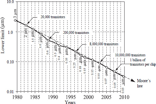
The evolution of technologies leading to this increasing integration is fast. It follows an empirical prediction made by Gordon Moore (cofounder of Intel), of an integration doubled every 18 months. Unequalled fact in any industrial sector, this technical evolution of the products has lasted for four decades (see Figure 1).
The manufacturing technologies of electronic components have evolved a lot since the invention of the first transistor: we went from an element the size of a 1€ coin to submicron dimensions (45 nm previewed at IBM in spring 2006, while in December 2007, the TSMC group sampled SRAMs in 32 nm technology. Nowadays, we are heading for 22 nm and below).
Nevertheless, some principles have been preserved, and of course the technology is subjected to constraints, resulting from the fundamental properties of the semiconductors, such as they appear in the chapters on the components' physics. Let us note however that 32 nm noticeably represents the thickness of a hundred atomic lines, and that we imperceptibly come near a limit below which we will no longer be able to go, except by completely changing the principles.
Figure 1. Moore's law
Surprisingly, there are no works written in the French language describing these 30 years of history and evolution of technological methods. We can remember:
— that the evolution of CMOS technologies is made up of incremental and radical evolutions;
— that the control of these radical evolutions gives place to the highest costs and are the object of strategic decisions.
We often find a good number of precise publications on each topic, but little or no scientific summaries outlining the “why and how” of the various technical choices.
Among these key points, we have often quoted, over the last ten years:
— around the year 2000, for 130 to 90 nm nodes:
— around the year 2005, for 65 to 45 nm nodes:
- dipping lithography: with this, we can go down below 65 nm. Its unit piece of equipment exceeds 50 million dollars;
— around 2010, for 32 to 22 nm nodes:
— around 2014, for the 18-12 nm node:
All these stages use new techniques and thus new investments. We forget to name the advances made in the course of time by elementary methods, with the constant objective to decrease all dimensions (width, length, thickness) and to increase all the electrical performances (current, speed, low consumption, etc.).
This book thus proposes to the reader a timeline, of the development of active zones, modifying the surface structure of the massive silicon substrate, the basic principles, the implementations according to the technological fields, the limits and constraints, with a focus on the recent advances.
Its objective is not to go through the issue exhaustively for all the elementary processes of a technological assembly, but to point out the essential and fundamental pieces of data, only for the methods aiming to use and to improve the properties of the material or of the silicon semiconductor, for the electronic components, as well as for the microsystems (integrated sensors for example).
Below, a few paragraphs introduce each of the four matters evoked, but leave to the authors (J.J. Ganem, I. Trimaille, J.J. Grob, D. Mathiot and J.M. Hartmann, the best French-speaking specialists on the topic), the pleasure of elaborating on the manufacturing methods and scientific materials (physical and chemical laws),which consolidate or predict the outcomes.
Silicon oxidation
Oxidation is a very important stage in the achievement of integrated silicon circuits, because it is thanks to this specific property that the silicon, which is not a priori a very good semiconductor, has become the most frequently used material in microelectronics. This operation is necessary throughout the modern manufacturing methods of integrated circuits. It is thus essential to know how to carry out an oxide of good quality.
The oxide can be used as:
— an implantation and diffusion mask of dopants;
— a passivating layer on the silicon surface;
— insulation zones between various components of an integrated structure;
— an active zone in MOS (gate oxide) transistors;
— electrical insulation between the adjacent layers to improve the integration and the reduction of dimensions (“spacer” for example, see further);
— electrical insulation between the various levels of metallization or of conducting layers in strongly doped polycrystalline silicon;
— sacrificial layers that can improve the circuit performances and integration. These sacrificial layers can also be used to manufacture microstructures containing polycrystalline silicon and to intervene in integrated microsystems (MEMS: micro electro-mechanical systems).
Ion implantation
Ion implantation is a low-temperature process. The implantation process takes the ions of the chosen species, accelerates them with an electrical field, and then makes them scan the surface of the slice, to carry out a uniform pre-deposition.
This method of introducing doping atoms into silicon was developed in the 1960s: it is ion implantation (an ion is a loaded atom). Very briefly, the ion implantation consists of projecting the ions of the adequate doping species towards the slice, through the openings of an oxide mask or of hardened resin.
The ions used for the doping, such as boron, phosphorus or arsenic, are generally produced from a gas source, guaranteeing a great purity of the source. These gases have a tendency to be very dangerous. When they are implanted in a semiconductor, each doping atom creates a charge carrier (hole or electron according to whether it is a type p or n dopant), thus locally altering the conductivity of the semiconductor.
The ion implantation is also a method used for the preparation of SOI (silicon-on-insulator) substrates from conventional silicon substrates.
Diffusion
Diffusion is the term used to describe the movement of atoms, molecules or particles from a high concentration zone towards a lower concentration zone.
Diffusion is a phenomenon, depending on time and temperature. The diffusion velocity of an atom, molecule or compound from an area of high concentration towards a low concentration zone is a function of time and temperature. The parameter connecting the diffusion velocity to the temperature at a given time, is known as the diffusion or diffusivity coefficient.
The atoms of the dopant must move the silicon atoms of the crystalline structure and take their place to become electrically active. The diffusion process is used in the manufacture of integrated circuits, in order to introduce a controlled quantity of a specific dopant into a specific area of the semiconductor crystal. The diffusion process used to achieve this substitution is divided into distinct stages.
Epitaxy of strained Si/Si1-xGex hetero-structures
The term epitaxy is of Greek origin and means “to build above”. Deposition by epitaxy is in general the construction of a single-crystal silicon layer on a slice (also a single-crystal). The layer deposited is a crystallographic extension of the substrate, from the point of view of the atomic arrangement (i.e. identical crystalline structure). The substrate can thus be regarded as the “seed” essential to generate a single-crystal growth.
Deposition by epitaxy is a process of CVD. The first use of CVD was the single-crystal silicon deposition at the end of the 1950s. This technique then played a crucial role in this industry, but this chapter will not develop the aspect “material -growth and crystallography of silicon substrates”, instead focusing on the use of the epitaxy technique for the manufacture of active SiGe zones in nano-CMOS new technologies.
We hope that by introducing a comprehensive overview of these techniques to readers, this book will answer the expectations of those students, professors, technicians, engineers or researchers, closely interested in the manufacture of silicon micro nanostructures.
This preface would not be complete without extending to the authors, J.J. Ganem, I. Trimaille, J.J. Grob, D. Mathiot and J.M. Hartmann, my warmest thanks for their rich contributions to this book.
Annie BAUDRANT
May 2011