
Chapter 4
Epitaxy of Strained Si/Si1-x Gex Heterostructures 1
4.1. Introduction
4.1.1. General introduction
This chapter discusses the reduced pressure-chemical vapor deposition (RP-CVD) of Si/SiGe (C) heterostructures for nanoelectronics and opto-electronics. The chapter is structured as follows. Section 4.1 will present: (i) the development since the beginning of the industrial CVD of Si and SiGe; (ii) the epitaxy tool used in CEA-LETI to carry out studies described in this chapter; and (iii) some general concepts of epitaxy which will be useful later on. The epitaxy of strained Si/Si1-xGex and Si/Si1-yCy heterostructures as conducting channels of pMOS and nMOS transistors, will be detailed in sections 4.2 and 4.3. The selective epitaxial growth on SOI substrates of Si or SiGe(:B) recessed and raised sources and drains will be described in sections 4.4 and 4.5.
In section 4.6, we will present the structural properties of (i) SiGe virtual substrates and the tensily-strained Si layers grown on top and (ii) the sSOI substrates resulting from them. We will also focus on the electric gains (thanks notably to dual channels) in nMOS and pMOS transistors built on top. The structural, electric and optical devices properties of thick Ge layers and of Ge islands on Si(001) will be described in section 4.7. We will highlight in section 4.8, the exciting possibilities offered from an architectural point of view by the lateral selective etching of SiGe sacrificial layers. Finally, the most outstanding results will be summarized in section 4.9 and some prospects will also be presented.
4.1.2. Chemical vapor deposition from the beginning
This section is freely inspired by the recent article by W.B. De Boer [BOE 08], one of the founding fathers of modern industrial epitaxy, who worked at ASM in the years 1980–1990 and who took part in the development of the Epsilon tool.
4.1.2.1. Introduction
Chemical vapor deposition (CVD) of Si is a relatively old technique of the semiconductor industry. It was originally used in bipolar transistors in order to deposit at high temperatures (typically 1,000–1,200°C) a high resistivity (i.e. intrinsic) Si thick layer on strongly doped (by ion implantation) buried layers. We then have a high avalanche-breakdown current and a low collector resistance. Thanks to very low carbon and oxygen levels, the crystalline quality of the deposited Si layer is equal to or higher than that of the substrate. Potential difficulties like auto doping (exodiffusion of the dopants implanted beforehand in undesired zones), the appearance of slip lines (temperature non-uniformity on the surface of the substrate), etc., are known and controlled to a certain extent.
Despite its cost, epitaxy has also been introduced into the fabrication of metal-oxide-semi-conductor (MOS) transistors. The use of an epitaxial layer as the channel beneath the gate of small-size MOS transistors can indeed prove to be interesting for threshold voltage adjustment and carrier mobility boosting. It can in particular lead to the suppression of parasitic short-circuits between adjacent individual transistors, to the reduction of errors in memory cells, to higher quality gate dielectric, etc.
The most recent low-temperature epitaxy methods are very different from the conventional methods mentioned above. Deposition temperatures (typically 600–700°C) are indeed such that dopant exodiffusion is no longer a problem. We can thus obtain sophisticated doping profiles with a control within the nanometer of planar SiGe layers with a thickness of ten nanometers or less, etc. From the industrial point of view, optimizing low-temperature epitaxy methods lead to heterojunction bipolar transistors (HBT). The SiGe:C base layer with the suitable boron doping profile is then inserted between the emitter and the collector layers (Si in situ doped with arsenic or phosphorus), rather than ion implanted. We can also remember the recent adoption in mass production of recessed, in situ B doped SiGe sources and drains in order to boost (thanks to uniaxial compressive strain) the hole mobility in the Si channel of short gate length p-type MOS devices.
4.1.2.2. CVD in general
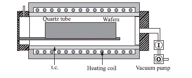
Atmospheric pressure-chemical vapor deposition (AP-CVD) was used in the 1960s in order to deposit SiO2, Si3N4 and Poly-Si layers. The need for minimizing deposition temperatures and for improving the methods led to the development of the low pressure CVD (LP-CVD) in the middle of the 1970s. The transport of active chemical species towards the surface of the Si substrate is thus improved (with the increase in their mean free path), leading to a much better deposition uniformity on a wafer and wafer to wafer and to a decrease by two orders of magnitude of gases consumption. The layout of the reactors has evolved, going from cold walls (wafers parallel to the gases flow) to hot walls (wafers vertically laid out side by side and perpendicular to the gases flow), as illustrated in Figure 4.1. The time deposition, longer in LP-CVD, is compensated by the more significant number of processed wafers, leading to a drastic process/wafer cost cut.
A new technology, the so-called Plasma-Enhanced CVD (PE-CVD), was developed a short time after LP-CVD. It enabled to reduce the deposition temperature even more by dissociating the decomposition of the gaseous precursors and their actual deposition on the surface. SiO2, Si3N4 and Poly-Si layers can thus be deposited at temperatures lower than or equal to 400°C, i.e. several hundred degrees below the temperatures commonly used in LP-CVD.
Figure 4.1. Schematic description of a horizontal LP-CVD reactor
4.1.2.3. High temperature conventional Si epitaxy
Conventional Si epitaxy methods (with atmospheric pressure and with chlorinated precursors such as SiCl4) were (and are still) characterized by very high deposition temperatures (1,000–1,200°C), inducing a marked inter-diffusion of the dopants between the epitaxial layer and the substrate. The interfacial zone, where the doping level changes will vary from a few hundred nm up to several microns, depending on the process conditions and the doping species used. The situation is complicated by the doping atoms, released by the surface or by the rear face of the wafer, which are re-deposited in the epitaxial layer (“auto-doping”), enlarging the depletion layer. The adoption of reduced pressures (50–100 Torr) at the end of the 1970s drastically reduced the n-type dopants (i.e. As or P) auto-doping and became standard for bipolar transistor epitaxy (on As doped buried layers). The pre-epitaxy surface preparation was also improved. High temperature HCl etching of a few thousand Å of Si, used in the 1960s and 1970s as surface preparation for bipolar transistors, was replaced by a H2 bake, which can remove the native oxide.
4.1.2.4. Low-temperature Si and SiGe epitaxy
The high deposition temperatures used in “conventional” epitaxy have always been troublesome. A large number of researchers tried at the beginning of 1980s to reduce them. The ideas explored were as follows: (i) plasma-assisted epitaxy (decomposition of the gaseous precursors using a remote plasma and not on the surface of the wafer); (ii) adoption of gaseous precursors (like SiH4) decomposing at lower temperature; (iii) the use of carrier gases other than hydrogen, such as argon or helium, etc. The problem with low temperature deposition was (and to a certain extent remains) the crystalline quality of the layer.
Meyerson et al. (IBM), thinking that the residual oxide on the surface was the limiting factor for the low-temperature growth of good quality epitaxial layers, proposed at the beginning of 1980s to call upon Ultra-high vacuum CVD (UHV-CVD), in order to avoid surface re-oxidation during epitaxy. The native oxide was removed ex situ, the wafers were loaded in the epitaxy tool and good crystalline quality Si layers were deposited at temperatures which can be lower than 500°C. It was very innovative at the time. Similar quality Si layers were at the same time obtained by Sedgewick et al. (IBM) with atmospheric pressure at temperatures of about 700°C. Process conditions were conventional and included an in situ H2 bake before epitaxy. What changed the situation was the adoption of advanced Pd purifiers (maximal water and oxygen concentrations: ten parts per million) for carrier gases, as well as a greater purity of precursor gases.
The difference between the extremely low partial pressures of oxygen and water necessary in UHV-CVD and the much less important constraints in more conventional CVD industrial equipment is due to the presence of large amounts of ultra-pure hydrogen, the carrier gas. The surface coverage by hydrogen atoms is then high at low temperature, passivating the surface with respect to impurity adsorption and incorporation, enabling the epitaxy of Si or SiGe layers of good structural and electronic quality.
Some of the problems of the high temperature conventional epitaxy disappear at low temperatures. The appearance of slip lines is no longer a problem. Boron auto-doping disappears and very abrupt boron doping profiles can be obtained. Si/SiGe heterostructures with morphologically as well as chemically abrupt interfaces can be deposited. Phosphorus doping is however more difficult at low-temperature and arsenic doping profiles are uncontrollable. Carbon is otherwise troublesome in high temperature epitaxy. An important surface concentration in C atoms generates the presence of SiC crystallites at the interface and thus of epitaxy defects. At low-temperature, C atoms can however be introduced in a substitutional way into the Si crystal lattice, inhibiting the diffusion of B dopants. This property is industrially used in HBTs in order to maintain the square B doping profile of the base layer (which is then a SiGeC:B alloy) during subsequent high temperature process steps. Low-temperature CVD, which is characterized by comparatively low growth rates, is complementary to the high temperature CVD and can be currently carried out in the same equipment.
4.1.2.5. Development of CVD equipment
Figure 4.2. Horizontal typical CVD reactor
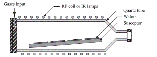
The horizontal atmospheric pressure reactor schematically described in Figure 4.2, was the choice equipment at the beginning of the semiconductor industry. The wafers were placed on a graphite susceptor and the gases flowed in a quartz chamber. The heating was ensured by RF filaments wrapped around the chamber, or by high intensity lamps focused on the susceptor, which radiated through quartz. For some applications, a resistive heating was directly installed in the susceptor. The walls were cooled, in order to minimize deposition on them. This was usually done with air, but also with water (tube with double inner surfaces). The most sophisticated reactors were characterized by a susceptor tilted upward, in gas output, in order to increase its speed and to compensate for the depletion in the gaseous phase. The reactors evolved during the transition from the AP-CVD to the CVD at reduced pressure (RP-CVD). We can notably mention the barrel reactors appearance, with a susceptor in the shape of a pyramid in a vertical tube (see Figure 4.3). Contrary to a horizontal reactor (which would immediately collapse), barrel reactors could be used at reduced pressure (50 – 100 Torr), thanks to vacuum pumps. After it was demonstrated that reduced pressures decreased the n-type auto-doping, this type of reactor became standard for the epitaxy of bipolar transitors and was used for many years.
Figure 4.3. RP-CVD barrel reactor
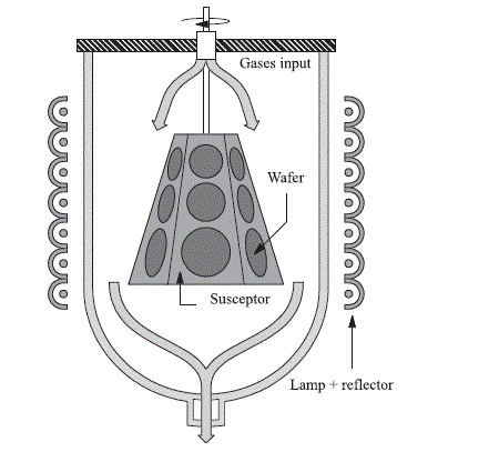
UHV-CVD reactors were introduced in the 1980s for low-temperature depositions, with a certain number of adjustments for the management of the ultra-high vacuum and to obtain very low partial pressures of contaminants. At the same time, manufacturers of industrial epitaxy reactors started to develop the next generations of equipment, i.e. large size high capacity reactors (increase of the wafer diameter), hardly different from the one described schematically in Figure 4.3. They were then focused on obtaining several µm thick p-type Si layers on p+ Si layers.
Another type of reactor was developed during these years. This reactor closely looked like the horizontal lamp reactor schematically shown in Figure 4.2, with the following specificities: a single wafer chamber with rotation of the wafers during the process, in order to compensate for gas phase depletion and thus generate a good deposition uniformity. A heating by lamp was combined with a low thermal inertia susceptor to achieve an acceptable output. Loading/unloading (also called “loadlock”) chambers, as well as a transfer chamber were added, to improve the cleanliness of the deposition chamber, essential for good quality of the epitaxial layers.
Indeed, the walls and valves of the deposition chamber are no longer in contact with the ambient air during loading/unloading steps, and thus not in contact with oxygen or moisture, for weeks or even months. More powerful than batch (i.e. multi-wafers) reactors in terms of uniformity and crystalline quality, these single-wafer reactors became competitive or even superior in terms of cost per wafer for diameters higher than or equal to 150 mm. The ability to operate at low pressure was added later on.
We will find a schematic description in Figure 4.4.
Low-temperature Si and SiGe epitaxies were tried in this type of reactor, with more convincing results, even with atmospheric pressure. Two types of deposition reactors were thus in competition for low-temperature depositions at the beginning of the 1990s: dedicated UHV-CVD batch reactors and single wafer RP-CVD reactors as in Figure 4.4, also able to operate at high temperature. It was not really difficult to choose between these two technologies, given the flexibility and the ease of use of single-wafer reactors.
Figure 4.4. Example of a modern epitaxy reactor: the ASM Epsilon
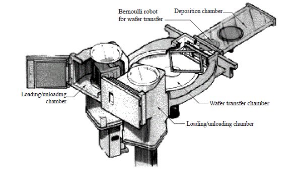
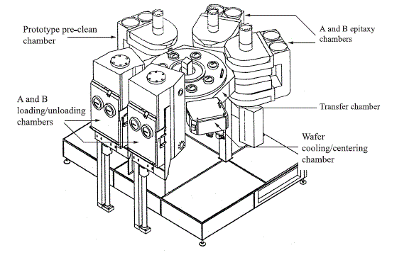
4.1.3. The Epi Centura epitaxy tool
In 1999, CEA-LETI acquired an Epi Centura 200 mm epitaxy mainframe from Applied Materials. This is what we call a cluster tool, i.e. a Centura platform on which two RP-CVD chambers called A and B are connected (see Figure 4.5). We find on the platform two loading/unloading chambers (“Loadlocks A and B”), which can hold up to twenty five 200 mm plates. These loadlocks, exposed to the air of the clean room during the wafer loading/unloading, are pumped down then re-filled with N2 several times prior to 20 pressure stabilization, i.e. the pressure of the transfer chamber. Given nitrogen, as well as hydrogen, the carrier gases used during epitaxy are of high purity (about 99.999999% after going through gases purification cartridges), the wafers stored in loadlocks are in an inert environment, which has its importance after an ex-situ “HF-last” wet cleaning. The “frog” robot located in the transfer chamber (in which 15 standard liters per minute of N2 flow continuously) enables the horizontal movement of wafers between the various chambers. Wafer removal from / deposition on the robot quartz blade or the peripheral chambers (i.e. movements according to z) is individually ensured in each one of those. The wafer cooling and centering chamber makes it possible: (i) to take into account upcoming movements between chambers, the minor alignment defects of the wafers on the quartz blade of the transfer robot and (ii) the postdeposition cooling of the wafers (thanks to a thick chuck with water circulation) before putting them back in the plastic baskets of the load locks. Before describing more precisely the epitaxy chambers, we will note the presence of a certain number of peripheral pieces of equipment, vital for the functioning of such a facility, such as: (i) the electronic control cabinet which also delivers the power to the lamps, (ii) a pressure-lowering cabinet for the various gases used, (iii) pumping lines and four pumps (in the basement) to control the pressure in the different chambers, (iv) a burning/scrubbing system for used gases (in the basement downstream of the pumps), (v) cabinets containing the various gas bottles, etc. It is indeed an expensive installation (approximately 4 million dollars for the whole) and it is complex to implement.
We will find in Figure 4.6 a schematic description of the two epitaxy chambers connected to our system. Approximately 40 cm in diameter, they are physically delimited by two transparent quartz domes (in light gray on the figure), solidarized to a circular metal support using clamp rings (both in dark gray on the figure) crushing Viton or Teflon gaskets (in order to withstand high temperatures). During epitaxy, the substrate lies horizontally on a slightly hollowed graphite susceptor covered with SiC (horizontal thick line on the figure). A rather complex system of arms enables, thanks to the robot fastened at the bottom of the lower dome: (i) the independent or joint wafer and susceptor upward and downward movements (in order to load or unload the wafer) and (ii) the rotation of the {susceptor + wafer} assembly (30 turns per minute), in order to achieve a satisfactory spatial homogeneity of the deposited layers. The carrier and process gases are injected in a laminar way just above the surface of the wafer (input and output through quartz inserts), with the possibility to adjust the center to edge uniformity with micrometer screws. Their thermal decomposition on the surface is ensured with the help of two banks of 20 lamps able to deliver up to 2 kW each (a bank above and one below the chamber). In order to ensure a better spatial uniformity of the temperature, the heating zones are divided into two parts. Eight lamps out of the 20 of each bank point towards the center of the wafer, the 12 remaining towards its periphery (vertical and oblique beams on the figure). The control of the temperature is ensured with the help of two infra-red pyrometers, one looking directly at the surface of the wafer (#1), the other looking at the backside of the susceptor on which the wafer lies (#2).
Figure 4.5. Schematic description of the Epi Centura epitaxy cluster tool. The prototype low-temperature H2 surface preparation chamber is no longer in service
In a simplified way, these pyrometers operate according to the principle of the blackbody: the power radiated P is collected and converted in temperature T, using a law of power P =σT4, with σ ~ 0.65 for Si and ~ 0.8 for graphite covered by SiC. Concretely, the lower pyrometer is usually used to control the growths The large surface emissivity fluctuations related to the use of blanket or patterned. substrates, the upper dome wall clogging during deposition the presence of a buried oxide etc indeed make the higher pyrometer temperature, readings unreliable. The cooling of the whole chamber is ensured by: (i) water circulation loops inserted in metallic elements and (ii) a very important volume of air circulating (using a ventilator) in a loop around the chamber quartz walls. The growth pressures, accessible with this configuration of chamber (and pumps) are in the range of 10 – 600 Torr (atmospheric pressure = 740 Torr). The pressure is controlled thanks to a 1,000 Torr Baratron gauge and a butterfly valve at the output of thechamber. The growth temperature range is between 350°C (minimal temperature for a reliable reading of the temperature by the pyrometers) and 1,100°C (maximal temperature not generating long-term deterioration of the air tightness gaskets).
Figure 4.6. Schematic description of the epitaxy chamber and artistic sight of a Si surface above which SiH4 molecules are arriving
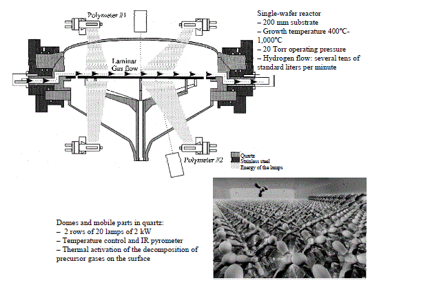
Epitaxy chambers are cold under N2 or hot under H2. The latter is indeed used as a carrier gas during growth. The important H2 mass-flow used (a few tens of standard liters per minute (slm), typically) lower the partial pressure of the gaseous impurities (typical rise in pressure of a chamber isolated from its pumping line: ~ 40 μTorr/min.) with values compatible with an epitaxy (i.e. some 10-10 Torr). Precursor Si gases are either pure dichlorosilane (SiH2Cl2), or pure silane (SiH4). We will use SiH2Cl2, if we wish to have a growth which is selective versus SiO2 or Si3N4 on patterned substrates. We will then deposit in the Si windows, not on these masking materials. SiH4 will be implemented when the growth does not have to be selective. We will then deposit single-crystal Si in the Si windows and polycrystalline Si on SiO2 or Si3N4. The Ge and C precursory gases are respectively germane (GeH4) diluted at 2% in H2 and monomethylsilane (SiCH6) diluted at 5% in H2. In order to n-type dope the crystalline matrix, i.e. to insert donor atoms which provide it with electrons, we will use phosphine (PH3), a precursor gas of P. Diborane (B2H6), the precursor gas of B, will be used for the p-type doping (i.e. insertion of atoms that capture electrons from the matrix, providing it with holes). Concentrations in PH3 and in B2H6, 2,000 parts per million (ppm) in the bottles (the dilution gas being H2), can be, should the need arise, modulated between 5.54 ppm and 367 ppm, thanks to mixers. There is thus a factor ~ 4,000 between the minimum and maximum mass-flows of pure diborane and phosphine that can be delivered in the chambers. The last gas to be available is gaseous hydrochloric acid (HCl). It is either used in order to increase selectivity on patterned wafers, or implemented at high temperature (1,200°C), high pressure (300 Torr) and with mass-flows of more than 10 slm, in order to clean post-epitaxy the domes’ quartz walls. We will note in the following of this chapter that the absolute values of the mass-flows are never given (in order to protect our know-how, considering that such a tool is commercially available). We can nevertheless say here that the maximal values of all the mass-flow controllers used to inject pure (SiH2Cl2, SiH4 or HCl) or diluted (GeH4, SiCH6, PH3 or B2H6) active gases in the chambers, range between 100 and 1,000 standard cubic centimetres per minute (sccm).
4.1.4. Some general concepts of epitaxy
Before talking about the results, we will recall here some definitions and concepts specific to epitaxy. Carrying out an epitaxy consists of depositing on a single-crystal substrate, a single-crystal layer adopting exactly the same crystalline structure as the structure of the substrate (case of III-V or IV-IV semiconductors crystallizing in the sphalerite or in the diamond structure, such as GaAs, Si, Ge, etc.), or a crystalline structure dictated by the substrate underneath, sometimes by means of rotations of the crystalline directions (metals on insulating substrates, etc.). We speak about homoepitaxy when the substrate and the deposited layer are of the same nature (for example: Si on Si). We speak about heteroepitaxy, when the substrate and the deposited layer are not of the same nature (for example: SiGe on Si).
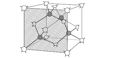
Si/SiGeC stacks in situ doped or not (we will speak about heterostructures) studied during these works, have most of the time been deposited on a Si substrate with a (100) surface (bulk-type or not (presence of a buried oxide layer), blanket or patterned, etc.). It thus appears useful at this stage to point out the essential features of the elementary components of a SiGeC alloy. Si, Ge and C all three crystallize in the diamond phase, i.e. two overlapping sphalerite structures shifted one from the other by a quarter of the large diagonal (see Figure 4.7).
Figure 4.7. Diamond structure and the usual (100) growth plane
The lattice parameter of C (i.e. the length of one of the cube edges in Figure 4.7) is much lower than that of Si, itself lower than the one of Ge ![]()
![]() This increase in the lattice parameter is accompanied by a significant decrease in the energy band gap: Eg (C) = 5.48 eV
This increase in the lattice parameter is accompanied by a significant decrease in the energy band gap: Eg (C) = 5.48 eV ![]() Eg (Si) = 1.11 eV
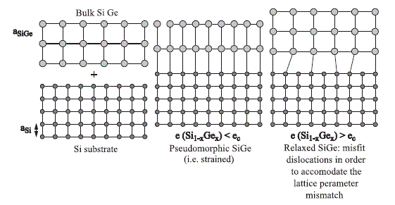
Eg (Si) = 1.11 eV ![]() Eg (Ge) = 0.66 eV). We thus conceive intuitively that mixing Si, Ge and C in a SiGeC alloy will induce important energy band gap modifications between these limiting values, as well as the built-in stresses (see sections 4.2, 4.3, 4.6 and 4.7). We will however keep in mind that it is extremely difficult to incorporate C in substitution into a Si or Ge array. The miscibility of C in Si is indeed only 10−4% at thermodynamic equilibrium (i.e. at 1,400°C), with an unfortunate tendency to form SiC precipitates for higher concentration values! On the other hand, Si and Ge are miscible in all proportions. During a heteroepitaxy, there will be in all probability a discrepancy in the lattice parameter between the deposited layer and the substrate. There will thus be an accumulation of elastic energy in it. For thin deposited thicknesses, atomic columns of the substrate will be extended in the epitaxial layer, then called pseudomorphic. A layer will be in tension (in compression), when its lattice parameter aL in its bulk state is lower (higher) than the one of the substrate. The in-plane lattice parameter being, for a pseudomorphic layer, equal to the one of the substrate
Eg (Ge) = 0.66 eV). We thus conceive intuitively that mixing Si, Ge and C in a SiGeC alloy will induce important energy band gap modifications between these limiting values, as well as the built-in stresses (see sections 4.2, 4.3, 4.6 and 4.7). We will however keep in mind that it is extremely difficult to incorporate C in substitution into a Si or Ge array. The miscibility of C in Si is indeed only 10−4% at thermodynamic equilibrium (i.e. at 1,400°C), with an unfortunate tendency to form SiC precipitates for higher concentration values! On the other hand, Si and Ge are miscible in all proportions. During a heteroepitaxy, there will be in all probability a discrepancy in the lattice parameter between the deposited layer and the substrate. There will thus be an accumulation of elastic energy in it. For thin deposited thicknesses, atomic columns of the substrate will be extended in the epitaxial layer, then called pseudomorphic. A layer will be in tension (in compression), when its lattice parameter aL in its bulk state is lower (higher) than the one of the substrate. The in-plane lattice parameter being, for a pseudomorphic layer, equal to the one of the substrate ![]() we have for a tensily-strained layer
we have for a tensily-strained layer ![]() and for a compressively-strained layer,
and for a compressively-strained layer, ![]() Indeed, the perpendicular lattice parameter is given by
Indeed, the perpendicular lattice parameter is given by ![]() with
with ![]() and
and ![]() However, when the thickness of the deposited layer is more important, it will at some point become energetically favorable to inject misfit dislocations in order to accommodate the lattice parameter mismatch and minimize the total energy stored. The layer will be called relaxed. The thickness, to which the transition from pseudomorphic to plastically relaxed layer occurs, will be called critical thickness for plastic relaxation. The various configurations of the {SiGe on Si} system is schematically illustrated in Figure 4.8.
However, when the thickness of the deposited layer is more important, it will at some point become energetically favorable to inject misfit dislocations in order to accommodate the lattice parameter mismatch and minimize the total energy stored. The layer will be called relaxed. The thickness, to which the transition from pseudomorphic to plastically relaxed layer occurs, will be called critical thickness for plastic relaxation. The various configurations of the {SiGe on Si} system is schematically illustrated in Figure 4.8.
Figure 4.8. Schematic illustration of atomic arrangement during an epitaxy of a SiGe layer on a Si substrate
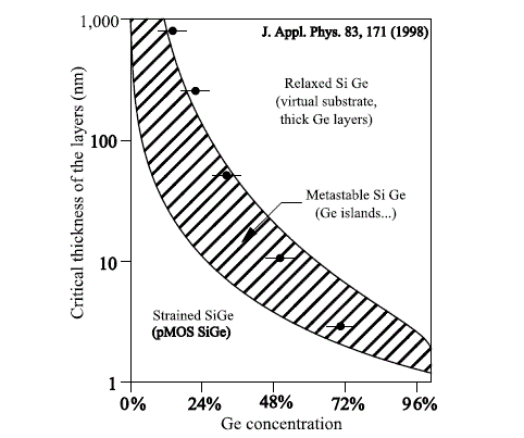
We represented in Figure 4.9 the critical thickness for plastic relaxation of SiGe on Si(100) as a function of the Ge concentration. The lowest curve corresponds to the critical thickness for plastic relaxation at thermodynamic equilibrium. It gives us the limiting values of the thickness not to be exceeded for SiGe layers deposited at (or submitted later on to) high temperatures. The highest curves, as well as the symbols, give us the critical plastic thicknesses associated with SiGe layers deposited at lower temperatures (and with significant growth rates). In fact, there are three thickness domains: (i) a domain of effective stability of the compressive stress below the critical thickness curve at the thermodynamic equilibrium; (ii) a metastability domain (hatched zone between the curves of Figure 4.9), where it will be necessary to pay attention to thermal budget minimization during growth and subsequent process steps, so that the layers remain in compression; and (iii) a high thickness domain for which SiGe layers will be partially, or even fully relaxed. It will be advisable to add for the high Ge concentrations and/or the high growth temperatures, an additional concept, i.e. the concept of critical thickness of elastic relaxation (located below the critical plastic thickness), above which the SiGe surface will become rough.
Figure 4.9.Critical thickness for plastic relaxation (in nm) as a function of Ge concentration for SiGe layers deposited on Si(100) substrates. It should be noted that the z scale is logarithmic!
SiGe has indeed this specificity, when it is compressively-strained on Si, to try to minimize the elastic energy stored by ripples of the growth front, as we will see in the following sections.
We will not describe furthermore the structural, as well as electric or optic properties of the SiGeC alloys. For further reading refer to the excellent works [CLA 07, CRE 06, DIM 07, KAS 00].
4.2. Engineering of the pMOSFET transistor channel using pseudomorphic SiGe layers
4.2.1. Introduction
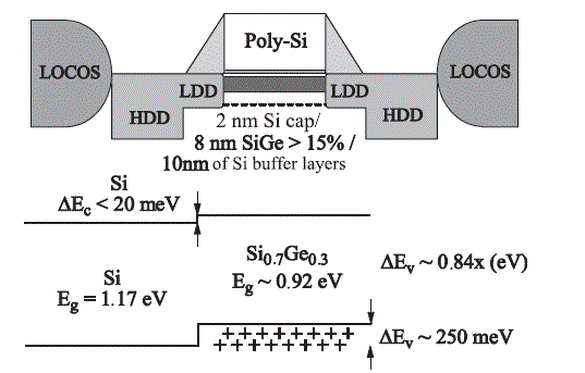
It can prove extremely interesting to insert under the gate of a pMOS transistor Si/Si1-xGex/Si stacks (see Figure 4.10), in order to benefit from holes mobility gains (factor of up to 2–3), associated with this type of heterostructure [SCH 97, WHA 98]. Because of the concentration in Ge and the compressive strain in the Si1-xGex channel induced by its pseudomorphic deposition on Si(001), a type II band alignment occurs between Si and Si1-xGex, with a small conduction band edge shift (about ten meV) and an important shift ΔEv of the valence band edge (the Si1-xGex layer behaving like a quantum well for the holes). Several studies have been devoted to the determination of ΔEv = Ev(Si1-xGex) − Ev(Si) according to the Ge concentration x. Van de Walle and Martin predicted in 1986 the following theoretical linear dependence: ΔEv = 0.84x (eV) [WAL 86]. From low-temperature photoluminescence measurements on Si1-xGex layers in compression, encapsulated by Si, Dutartre et al. [DUT 91] and Robbins et al. [ROB 92] obtained at the beginning of the 1990s, the following parabolic relations: ΔEv = 1.01 x − 0.835x2 (eV) and ΔEv = 0.874x − 0.376x2 (eV).
Figure 4.10. Schematic representation of a pMOSFET transistor of small length gate (sub. 0.1 µm) incorporating in the channel zone a Si/SiGe/Si stacking and an alignment of the valence and conduction bands between Si and Si0.7Ge0.3
From the epitaxy point of view, a certain number of pre-requisites must be answered, so that integration proceeds satisfactorily. First of all, it is essential that the growth takes place selectively compared to the insulating oxide, whatever the chosen insulation scheme (i.e. local oxidation of silicon – LOCOS, shallow trench isolation — STI, etc.). For that, we will have to use a chlorinated growth chemistry, i.e. SiH2Cl2 + GeH4 (with possibly the addition of HCl), combined with a low growth pressure (i.e. typically several tens of Torr). Once functioning points are acquired on blanket wafers (i.e. growth rate and Ge concentration for given mass-flows of the precursor gases, temperatures and pressures), the significant SiGe growth rate increase and the slight Ge content increase occurring when switching from blanket to patterned substrates with different size Si windows will have to be quantified (the so-called “global” and “local” loading effects). Finally, it will be advisable to reduce for high Ge contents the growth temperature, in order to avoid any elastic relaxation of the stresses accumulated in the Si1-xGex layer through the formation of a rough growth front. We will cover these various points in the following sections. We will then present the hole mobility gains that can be obtained in pMOSFETS transistors thanks to such stacks.
4.2.2. Growth kinetics of Si and SiGe in chlorinated chemistry
During the last ten years we have thoroughly explored Si and SiGe growth kinetics in chlorinated chemistry on (001) surfaces [HAR 02a, HAR 02b, HAR 03a, HAR 03b, HAR 04a, HAR 05a, HAR 07a]. As an example, we will look at the impact of the HCl mass-flow on the Si growth rate, at various temperatures and with dichlorosilane as a gaseous precursor. In the same way, we will quantify the influence of the HCl mass-flow on the SiGe growth rate and Ge concentration at 700°C, with dichlorosilane and germane as precursor gases. Lastly, we will briefly deal with the impact of growth temperature on the SiGe growth kinetics.
4.2.2.1. Growth kinetics of Si in chlorinated chemistry
Figure 4.11 presents the growth rate of Si as a function of the reverse absolute growth temperature for dichlorosilane only or for dichlorosilane + gaseous hydrochloric acid [HAR 02b]. These growth rates have been obtained via differential weighing of thick Si layers deposited on 200 mm Si(001) substrates. First of all, we notice the existence of two regimes, known as “high temperature”, controlled by the amount of precursor gases sent to the sample surface, and another one known as “low-temperature”, controlled by the desorption of the H or Cl atoms present on the surface. In the “high temperature” regime, the growth rate is dictated by the precursor gas mass-flow, as illustrated by the factor two on the growth rate between DCS/H2 = 0.0025 and DCS/H2 = 0.00125 mass-flow ratios. To add HCl almost does not decrease the growth rate in this regime, as we can see in Figure 4.2. An activation energy equal to 4.1 – 4.2 kcal.mol.-1 is associated with the low increase of the growth rate in this regime. The growth rate in the “low-temperature” regime, which strongly drops when the growth temperature decreases, is controlled by the number of dangling bonds not passivated by H or Cl atoms which are available for the adsorption and decomposition of the SiH2Cl2 molecules.
Figure 4.11. Arrhenius plot of the Si growth rate as a function of the reverse absolute growth temperature, for various SiH2Cl2 / H2 and HCl / H2 mass-flow ratios
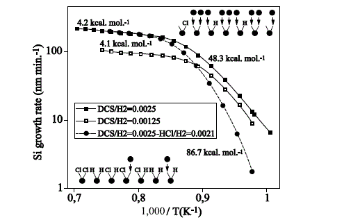
For this reason, we can note that the activation energy associated with the strong increase with temperature of the Si growth rate is for SiH2Cl2 only very close to the Si-H bond energy, i.e. 47 kcal.mol.-1 [SIN 89]. Meanwhile, the activation energy associated with the growth of Si thanks to a SiH2Cl2 + HCl chemistry, is close to the energy associated with the Si-Cl bond, i.e. 90 kcal.mol.-1 [GUP 90]. Adding HCl induces, for a fixed SiH2Cl2 mass-flow and at a given temperature, a significant drop in the growth rate. We modelled, based on the relationship suggested by Kongetira et al. [KON 97], the growth rate dependence on temperature and SiH2Cl2 and HCl mass-flows in the “low-temperature” regime (i.e. T < 1,100K). We found the following relationship [HAR 03a] (PDCS, PH2 and PHCl being the partial pressures in Torr of the gases in question):
![]()
4.2.2.2. Growth kinetics of SiGe in chlorinated chemistry
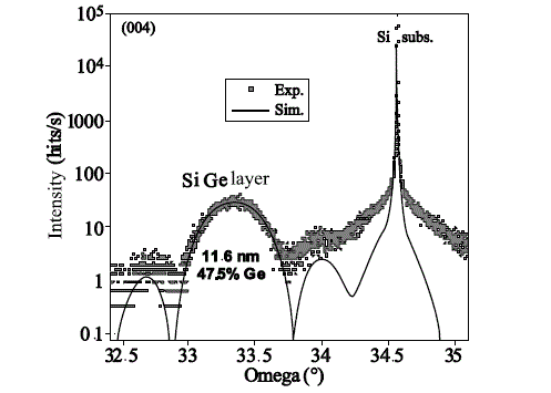
We have also studied the SiGe growth kinetics at 750°C [HAR 02a, HAR 02b], 700°C [HAR 03b], 650°C [HAR 04a], 600°C [HAR 07a] and finally 550°C [HAR 05a] as a function of the SiH2Cl2, GeH4 and HCl mass-flows. For these studies, we used high-resolution X-Ray diffraction (see Figure 4.12), to extract, for pseudomorphic SiGe layers deposited on Si(001), their Ge concentration (from the angular deviation between the peak associated with the Si substrate and the peak associated with the SiGe layer) and their thickness (from the angular width of the peak associated with the SiGe layer). In all cases, we could confirm the good crystalline quality of the layers (i.e. their pseudomorphic nature), thanks to the presence of thickness fringes on both sides of the SiGe layer peak. The nominal thickness of the SiGe layer was of course reduced when its Ge concentration increased, so that it always remained below the critical thickness for plastic relaxation [HUA 98].
Figure 4.12. Standard ω-2θ scan around the (004) X-Ray diffraction order for a 11.6 nm thick Si0.525Ge0.475 layer deposited at 550°C on Si (001)
We will find in Figure 4.13 the Ge concentrations and the SiGe growth rates obtained at 700°C, 20 Torr for fixed SiH2Cl2 mass-flows (F(SiH2Cl2) /F(H2) = 0.0025 or 0.01) and variable GeH4 and HCl mass-flows [HAR 03b]. The dependence of the Ge concentration on the F(GeH4)/(F(SiH2Cl2) + F(GeH4)) mass-flow ratio is sub-linear. The addition of HCl leads, for given SiH2Cl2 and GeH4 mass-flows, to a clear Ge concentration increase. Lastly, there is a strong discontinuity between the F(SiH2Cl2)/F(H2) = 0.0025 and F(SiH2Cl2)/F(H2) = 0.01 Ge concentration curves, which seems related to a reaction of order 2 regarding the SiH2Cl2 adsorption, compared to a reaction of order 1 for the GeH4 adsorption [ITO 95].
Figure 4.13. Ge concentration (on the left) and SiGe growth rate (on the right) at 700°C, 20 Torr as functions of either the F(GeH4)/(F(SiH2Cl2) + F(GeH4)) or the F(GeH4)/F(H2) mass-flow ratios, this for two SiH2Cl2 mass-flows (F(SiH2Cl2)/F(H2) = 0.0025 or 0.01) and various HCl mass-flows (see figure inserts)
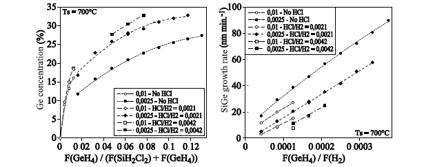
We note a very marked, almost linear-increase of the SiGe growth rate, when the F(GeH4) /F(H2) mass-flow ratio increases. This increase is related to a major decrease in the H and Cl atoms surface coverage when Ge atoms are chemically adsorbed on the surface. The latter indeed act as preferential desorption centers of the H or Cl atoms on the surface, freeing sites for the adsorption of SiH2Cl2 and GeH4 molecules. Indeed, energies associated with the Ge-H and Ge-Cl bonds, 37 kcal. mol.-1 [SUR 84] and 51 kcal. mol.-1 [KAM 98], are much lower than the binding energies of Si-H and Si-Cl, 47 kcal. mol.-1 [SIN 89] and 90 kcal. mol.-1 [GUP 90]. Adding HCl induces the formation of chlorides, chlorosilanes and chlorogermanes in the gaseous phase, decreases the quantity of Si or Ge atoms available for incorporation, and thus generates an important drop in the growth rate [CHA 87, KNU 94].
We illustrated in Figure 4.14 the influence of the growth temperature on the growth kinetics of SiGe with a SiH2Cl2 + GeH4 chemistry (without HCl) [HAR 03b]. An increase in the growth temperature generates, for given SiH2Cl2 and GeH4 mass-flows, a very clear increase in the growth rate, correlated to a significant decrease of the Ge concentration. From Arrhenius plots of the SiGe growth rate functions of the reverse absolute temperature, it is possible to go back up to the associated activation energy in the temperature range 550°C-650°C. This energy decreases in an almost linear way from 57 to 41 kcal. mol.-1, when the concentration (at 600°C) goes from 18% to 44% [HAR 07a].
Figure 4.14. Ge concentration (on the left) and SiGe growth rate (on the right) at 750°C, 700°C or 650°C as functions of either the F(GeH4)/(F(SiH2Cl2) + F(GeH4)) or the F(GeH4)/F(H2) mass-flow ratios, this for two SiH2Cl2 mass-flows (F(SiH2Cl2)/F(H2) = 0.0025 or 0.01). Growth pressure was 20 Torr
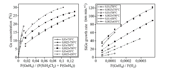
Figure 4.15. Parameter n as a function of the F(HCl)/F(H2) mass-flow ratio, at various growth temperatures and for two F(SiH2Cl2)/F(H2) mass-flow ratios: 0.0025 and 0.01
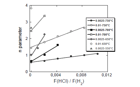
Regarding the x concentration in Ge, its dependence according to the F(GeH4)/(F(SiH2Cl2) mass-flow ratio can satisfactorily be modelled by the following relation: x2/(1−x) = n * F (GeH4 )/ (F (SiH2Cl2) [SUE 00]. We reported in Figure 4.15 the n values thus obtained. The higher n is, the higher the concentration in Ge will be for given precursor gas mass-flows. It is confirmed that the higher the HCl flow is and the lower the growth temperature is (in the range 550°C-750°C), the higher n will be.
As an additional element, we will note an almost linear increase of n with the F(HCl)/F(H2) mass-flow ratio, with a steeper slope when the growth temperature decreases. In addition, we will note that it is possible to model the dependence in temperature of n with a given HCl flow, with laws of the n = n0 *exp(−Ea/kBT) type, with negative “activation energies”. As an example, we find n = 7.6x10⁻⁴ exp(13.3 kcal. mol.-1/kBT) for F(SiH2Cl2)/F(H2) = 0.0025 and F(HCl)/F(H2) = 0 in the range 550°C-750°C. This value of -13.3 kcal.mol.-1 is very close to the value (-14 kcal. mol.-1) for growth pressures lower than 20 Torr found by Sue and Lee [SUE 00].
4.2.3. Transposition on patterned substrates
As mentioned in the introduction, during the transition from blanket to patterned substrates with variable windows sizes, we are confronted with several phenomena proving to be extremely annoying to obtain planar SiGe layers of controlled thickness and concentration.
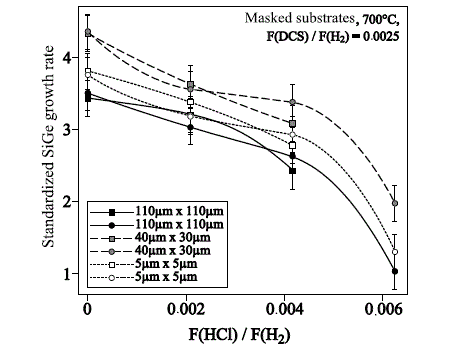
First of all, there are loading effects of two natures: global (strong increase of the growth rate and slight increase of the Ge concentration, while going from blanket to patterned substrates) and local (fluctuation of the growth rate and the concentration, when the Si windows size fluctuates) [BOD 97, GIA 03, HAR 03c, HAR 04a, HAR 05a, ITO 95, KOL 09, MEN 01]. As an example, we have reported in Figure 4.16, the standardized growth rates (i.e. the growth rate in a window divided by the growth rate on blanket substrate) obtained at 700°C, at given SiH2Cl2 and GeH4 flows and for variable HCl flows [HAR 03c]. First, we note that, for null HCl flow, we have an increase by up to a factor 4 of the growth rate, due to a very important surface coverage (with this mask) by SiO2: 92%. Adding HCl however makes it possible to appreciably reduce the increase of the growth rate. Lastly, we will note that the standardized growth rate fluctuates with the windows size. This growth rate increase is a function of the surface coverage by the dielectric masking material.
There is for example a standardized growth rate equal to 1.2 only for a 40% surface coverage by SiO2 [HAR 04a]. In addition, we have highlighted (using a study in spectroscopic ellipsometry) a Ge concentration increase fluctuating between 2% and 4%, when switching from blanket substrates to large windows on patterned substrates [HAR 04a]. It is thus suitable to gauge for each mask type the loading effects, global as well as local. We can also be confronted with elastic strain relaxation via the formation of surface undulations when switching from blanket to patterned substrates [BAS 01, HIK 09, MEN 03].
Figure 4.16. Standardized SiGe growth rates in Si windows of variable size (110 µm x 110 µm, 40 µm x 30 µm, 5 fim x 5 µm) functions of the F(HCl) / F(H2) mass-flow ratio for the following F (SiH2Cl2) / F(H2) and F(GeH4) / F(H2) mass-flow ratios: 0.0025 and 1.25x10⁻⁴ (circles) and 0.0025 and 1.67x10⁻⁴ (squares). Growth temperature and pressure: 700°C and 20 Torr. Associated Ge concentrations, functions of the HCl and GeH4 flows, were on blanket wafers in the 18% - 32% range
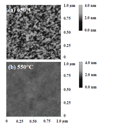
To minimize the elastic relaxation, the growth temperature T should be lowered, when the Ge concentration of the layers to be deposited increases. Quantitatively, it is possible to selectively grow smooth, approximately 10 nm thick Si0.85Ge0.15 layers with T≤750°C. For Si0.75Ge0.25, it would be desirable that T ≤ 650°C. For Si0.65Ge0.35, growth temperatures lower than or equal to ~ 600°C should be chosen. This is clearly illustrated in Figure 4.17, for 10 nm thick Si0.65Ge0.35 layers deposited selectively either at 650°C or at 550°C on patterned ultra-thin silicon-on-insulator (SOI) substrates [HAR 05a]. The surface of the Si0.65Ge0.35 layer deposited at 650°C is rough (root mean square (rms) roughness = 4.9 Å), while the surface of the Si0.65Ge0.35 layer deposited at 550°C is smooth (rms roughness = 0.9 Å). Lastly, once SiGe/Si stacks are satisfactorily grown, the thermal budget that will be seen by the wafers later on should be minimized. It is indeed completely possible that the elastic stresses stored in metastable stackings during the growth can be released (at least partially) by misfit dislocations emission during activation anneals after ion implantation of sources and drains, during the in situ H2 bakes that are carried out prior to the growth of raised sources and drains, etc. We could also be confronted with chemical enlargements of the interfaces between Si and SiGe [HAR 03c].
Figure 4.17. 1 µm x 1 µm AFM images of the surface of (a) a 10 nm thick Si0.65Ge0.35 layer selectively grown at 650°C and (b) an 11 nm thick Si0.65Ge0.35 layer selectively grown at 550°C inside the Si windows of patterned, ultra-thin SOI substrates
4.2.4. pMOS transistors incorporating SiGe layers
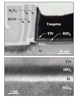
These last few years, we proceeded to the integration of Si/SiGe(C)/Si stacks in short gate length pMOS transistors. Two Ge concentrations have been tested: 19% with a conventional SiO2/Poly-Si gate stack [AND 03], and 28% with a more complex gate stack, i.e. HfO2/TiN/W [WEB 04a, WEB 04b]. The nominal thickness for the Si buffer and cap layers were respectively about 10 nm and 3 nm, while the SiGe layers had a thickness either of 15 nm (for 19% of Ge), or of 8 nm (for 28% of Ge). We will find in Figure 4.18 cross-sectional high resolution — transmission electron microscopy (HR-TEM) images of a pMOS transistor of the second type. First of all, we will note that the Si0.72Ge0.28 layer is planar and with a thickness close to the one aimed for [HAR 04a]. In addition, we will notice that the SiGe / HfO2 interface is relatively abrupt. This is the result of a thorough study undertaken by Damlencourt et al. [DAM 04a] on the impact of the surface preparation of SiGe (“HF-last” (type A) or covered with a thin chemical oxide (type B)) on the morphology of HfO2 layers deposited on top.
Figure 4.18. Cross-sectional TEM images of a SiGe 28% pMOS transistor with a metal gate (damascene architecture)
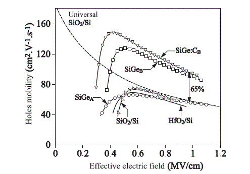
We represented in Figure 4.19 the holes mobility as a function of the effective electric field applied, for various gate stacks. Using a type B SiGeB/HfO2 gate stack makes it possible to obtain a mobility gain of 65%, compared to the universal reference SiO2/Si, and of 100% compared to HfO2/Si stacks [WEB 04a]. Moreover, we can notice that an inappropriate surface preparation of SiGe prior to HfO2 deposition (i.e. type A SiGe) generates a dramatic drop in the holes mobility. These studies also highlighted the need for reducing the thickness of the Si cap layer as much as possible, in order to avoid the appearance of a parasitic, lower mobility channel for holes at the Si/SiO2 or Si/HfO2 interface that would degrade the electric performances of sub-0.1 µm gate length transistors.
Figure 4.19. Holes mobility as a function of the effective electric field for various stacks: reference SiO2 / Si, HfO2 / Si, SiGeA / HfO2 and SiGe(:C)B / HfO2
4.3. Engineering of the nMOSFET transistor channel using pseudomorphic Si1-yCy layers; SiGeC diffusion barriers
4.3.1. Introduction
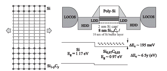
Although the gain in terms of electrons mobility in buried, tensily strained Si1-yCy channels still remains to be shown, it can prove to be interesting to insert Si/Si1-yCy/Si pseudomorphic stacks beneath the gate of n-MOSFET transistors. Because of the tensile strain present in Si1-yCy layers deposited on Si(001), there is indeed a partial lift of the degeneracy of the conduction band edge of Si1-yCy, with a twofold degenerated level then found below the conduction band edge of Si, and a fourfold degenerated level above it (see Figure 4.20). The edge discontinuity of the conduction band ΔEc. = Ec(Si) − Ec(Si1-yCy), being of about 6.5y (in eV) [SIN 99], a Si1-yCy layer inserted in Si will thus behave like a quantum well for electrons. The edge discontinuity of the valence band between Si and Si1-yCy is generally regarded as negligible.
We can also profit from the fact that the C atom is much smaller than those of Si or Ge, to compensate by the addition of C the compressive strain present in SiGe layers. Indeed, let us assume that the Si1-x-yGexCy lattice parameter is given by the following formula (which takes into account the nonlinear dependence of the lattice parameter with the Ge concentration and which has as a hypothesis a linear dependence on the Si1-yCy lattice parameter between Si and β -SiC): a (Si1-x-yGexCy) = 5.43105 + 0.2005x + 0.0263x2 − 2.1428y (in Å).We will easily check that 1% of C atoms in substitutional sites compensates for the compressive stress induced by 10.5% of Ge atoms.
Figure 4.20. Schematic representation of a short gate length (sub. 0.1 µm) nMOSFET transistor with in the channel region a Si / Si1-yCy / Si stack (with tensily-strained Si1-yCy layers) and alignment of the valence and conduction bands between Si and Si.097C0.03
C atoms incorporated in interstitial sites in SiGeC or Si1-yCy layers otherwise block B atoms diffusion. This can be advantageously used in order to obtain retrograde doping profiles, in particular under bulk nMOS transistors gates (where multiple B ion implantation steps are used to adjust their threshold voltage) [RUC 98].
From the epitaxy point of view, it is important to know that, contrary to SiGe, miscible in all proportions, it is difficult to incorporate substitutional amounts of C atoms higher than one percent in a Si or SiGe lattice. Indeed, the C atoms will then tend to be incorporated not only in substitutional sites, but also in interstitial sites or in the form of β-SiC nano-precipitates. To reach high substitutional concentrations in C, as we will see later on, we should work with the suitable chemistry at the lowest possible temperature with still reasonable growth rates. It will also be necessary to minimize the post-epitaxy thermal budget, in particular during annealing, in order to avoid the transition of C atoms from substitutional to interstitial sites.
Finally, we will see that, in the case of Si/Si1-yCy/Si stacks, it is essential to adopt an integration strategy, taking into account the non-selectivity of the deposition.
4.3.2. Incorporation of C in Si and SiGe
These last few years, we have worked a lot on the incorporation of C into Si and SiGe with either silane [HAR 02c, HAR 04b, HAR 05a, LOU 02, LOU 03a] or dichlorosilane as the Si gaseous precursor [LOU 03b]. We highlighted that a dichlorosilane chemistry made easier the incorporation of C in the substitutional sites of the lattice at given temperature and total quantity of C [LOU 03b]. We are however confronted, notably during Si1-yCy growth, with much lower growth rates for dichlorosilane than for silane at a given temperature. We will thus have to use a silane chemistry for the growth of high sunstitutional C concentration Si1-yCy and low Ge% SiGeC layers.
On the other hand, dichlorosilane chemistry will be chosen as soon as we wish to obtain high amounts of substitutional C atoms in SiGeC layers with percentages in Ge higher than or equal to 10%. First of all, we will take a look at SiGeC layers with concentrations in Ge higher than or equal to 10%. We will find in Figures 4.21 and 4.22, X-Ray Diffraction profiles and SIMS profiles, corresponding to SiGeC layers with 32% of Ge and a thickness close to 20 nm deposited at 550°C with a dichlorosilane chemistry on Si (001). We extracted from the XRD profiles, the concentrations in substitutional C atoms in our layers, by adopting a linear extrapolation between the lattice parameter of Si and that of β-SiC. First, we checked that the percentage of Ge was not altered in them, when the quantity of C atoms fluctuated. [LOU 03b]. SIMS profiles will provide us with the total concentration in C atoms (i.e. substitutional + interstitial).
Figure 4.21. ω -2θ profile around the (004) XRD order for SiGeC layers with 32% of Ge and variable substitutional C concentrations. Rf = F(SiCH6) / (F(SiH2Cl2) + F(GeH4))
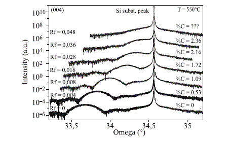
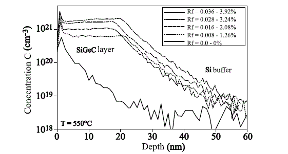
Figure 4.22. SIMS depth profiles of the total C concentration in various SiGeC layers with 32% of Ge Rf = F(SiCH6) / (F(SiH2Cl2) + F(GeH4))
We will find in Figures 4.23 and 4.24, concentrations in C atoms functions of the Rf = F(SiCH6) / (F(SiH2Cl2 or SiH4) + F(GeH4)), mass-flow ratio, with given Si gaseous precursor (F(SiH2Cl2 or SiH4) / F(H2) = 0.0025) and germane (F(GeH4) / F(H2) = 1.25x10⁻⁴) mass-flows and for various deposition temperatures (see Figure 4.23) or for various growth chemistry (see Figure 4.24). For low Rf values, almost all the C atoms are incorporated in substitutional sites. For higher Rf values, we have more and more interstitial C atoms, as attested by the growing discrepancy between the XRD and SIMS curves. Examining Figure 4.23, we notice that the lower the growth temperature is, the higher the quantity of C atoms in substitutional sites is. This tendency was confirmed, whatever the Ge concentration or the growth chemistry [HAR 04b, LOU 03a, LOU 03b]. Moreover, the use of a chlorinated growth chemistry leads to concentrations in substitutional C atoms which are higher than with a hydrogenated chemistry, as mentioned in the introduction and illustrated in Figure 4.24. We can thus reach for several tens of nm thick SiGeC layers, very high concentrations of substitutional C atoms: 1.42% for SiGeC 12% in Ge at 600°C, and 2.50% for SiGeC 32% at 550°C. These values are the highest reported nowadays in the literature for conventional Si precursors and growth strategies.
By comparison, Mi et al. have obtained (with the same hypothesis regarding the SiGeC lattice parameter) a maximum of 1.72% [MI 95]. The total quantity CT in atoms C incorporated into the lattice almost does not depend on the growth temperature (see Figure 4.23). For silane chemistry, its dependence function of Rf, is given by CT / (1−CT) = p[F(SiCH6) / (F(SiH4) + F(GeH4)), with p = 1.10 − 1.34 in the temperature range of 550°C — 650°C [LOU 03a]. For dichlorosilane chemistry, the dependence is not linear, as we can see in Figure 4.23. Experimental data are well accounted for with a CT1.4 / (1−CT) = q[F(SiCH6) / (F(SiH2Cl2) + F(GeH4)) relationship, with q = 0.28 – 0.34 in the temperature range of 550°C — 650°C [LOU 03b]. Regarding the growth of high C concentration Si1-yCy layers with silane chemistry, we highlighted the need to work at low-temperatures (i.e. 550°C), in order to maximize the concentration of C atoms in substitutional sites [LOU 03a]. Moreover, we showed that, at a given deposition temperature, it was extremely interesting to increase the absolute values of the silane and mono-methylsilane mass-flows, in order to increase the growth rate (from 0.4 to 1.3 nm min.-1), and to thus maximize the concentration of substitutional C atoms [HAR 04b, HAR 05a] (see Figure 4.25). We thus could obtain 15 nm thick Si1-yCy layers with 2.1% of C atoms in substitutional sites and only 0.1% of C atoms in interstitial sites. This value of 2.1% is the highest reported nowadays in the literature for the silane chemistry and this type of thickness (1.8% for Mitchell et al. [MIT 97]). Even higher concentrations of C atoms in substitutional sites, i.e. 2.8% [BAU 07], have recently been obtained thanks to trisilane (i.e. Si3H8), the liquid precursor of Si, and a cyclic {deposition/etch (with Cl2)} growth strategy. Trisilane indeed decomposes at temperatures much lower than silane [GOU 09a].
Figure 4.23. Carbon concentrations at 650°C, 600°C and 550°C either in substitutional (XRD) or in substitutional + interstitial (SIMS) sites, for the same flows of dichlorosilane (F(SiH2Cl2) / F(H2) = 0.0025) and germane (F(GeH4) / F(H2) = 1.25x10⁻⁴)
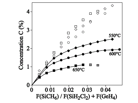
Figure 4.24. Concentrations at 550°C of C atoms in substitutional (XRD) or substitutional + interstitial (SIMS) sites, for the same Si and Ge precursor mass-flows (i.e. F(SiH2Cl2 or SiH4) / F(H2) = 0.0025 and (F(GeH4) / F(H2) = 1.25x10⁻⁴)
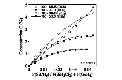
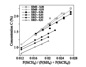
Figure 4.25. Concentrations at 550°C of C atoms in substitutional (XRD) or substitutional + interstitial (SIMS) sites functions of the F(SiCH6) / F(SiH4) mass-flow ratio, this for four different silane flows: F(SiH4) / F(H2): 0.01, 0.02, 0.03 and 0.06
4.3.3. Si/Si1-yCy/Si stacks for nMOS transistors
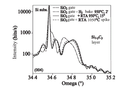
The aim being the integration of Si/Si1-yCy/Si stacks in nMOS transistors, we have studied their growth on patterned substrates and their stability with respect to various post-epitaxy thermal processes [HAR 02c, HAR 04b]. We will find in Figure 4.26, an AFM image of the surface of a patterned substrate after the deposition of a {Si buffer (10 nm) / Si0.984C0.016 (7 nm) / Si cap (3 nm)} stack at 550°C with SiH4. We note that, despite the adoption of a chlorinated chemistry for the growth of the Si buffer layer, depositing even 10 nm with silane does not make it possible to obtain selectivity with respect to SiO2, as attested by the high roughness of the LOCOS surface. However, we can notice that the surface roughness in the Si windows of the deposited stack is very low. The corollary of this lack of selectivity is the absence of any loading effect. We will find in Figure 4.27, X-ray diffraction profiles of Si/Si0.989C0.011/Si stacks having been subjected post epitaxy to various thermal process steps. We notice that the angular position of the peak associated with the Si1-yCy layer almost does not change, when a gate oxide has been formed and such stacks have been submitted to rapid thermal annealing. On the other hand, an in situ H2 bake at 950°C during 2 minutes (that would be used prior to the selective epitaxial growth of raised sources and drains) generates an important angular shift of the XRD peak towards low angles, characteristic of the transition of C atoms from substitutional to interstitial sites (formation most likely of SiC nano-precipitates). It will thus be necessary, as for Si/SiGe/Si stacks, to minimize the post-epitaxy thermal budget.
Figure 4.26. AFM image in the proximity of a window edge of a Si/Si1-yCy/Si stacking, confirming the absence of selectivity with silane chemistry (conservation of the step height and LOCOS surface roughness)
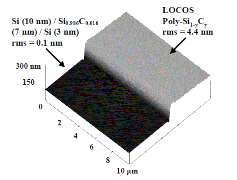
Figure 4.27. ω -2θ scans around the (004) XRD order for Si/Si0.989C0.011/Si stacks after various thermal process steps
We have also quantified the benefits of using such stacks as diffusion barriers for B. We will find in Figure 4.28, SIMS depth profiles of B in {poly-Si/SiO2/Si/Si1-yCy/Si/Si substrate pre-implanted with B} stacks. Whatever the concentration in C and/or the epitaxy temperature, we obtain thanks to the presence of C atoms a more retrograde B doping profile in the channel (drop by a factor which can go up to 100 of the concentration in B in this region) [HAR 02c, HAR 04b].
Figure 4.28. SIMS profiles of the concentration of B for various stackings under the gate
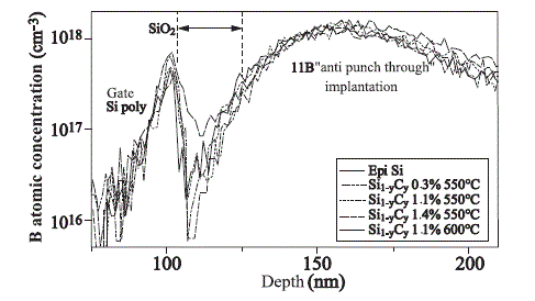
Figure 4.29. SIMS profiles of the concentration of C for various stackings under the gate
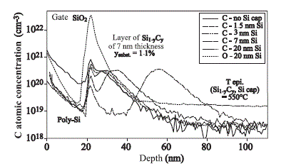
We have otherwise highlighted, from the electric point of view, the harmful influence of the C atoms, notably in interstitial sites, close to the gate [DUC 04a, ERN 02, ERN 03, WEB 03]. Finally, we have studied the impact of the Si cap layer thickness on the concentration of C atoms (see Figure 4.29). A drop by a factor 10 of the sheet concentration of C atoms in the SiO2 gate dielectric occurs when the thickness of the Si cap layer goes from 0 to 20 nm [HAR 04b].
4.3.4. nMOS transistors incorporating Si1-yCy layers or SiGeC diffusion barriers
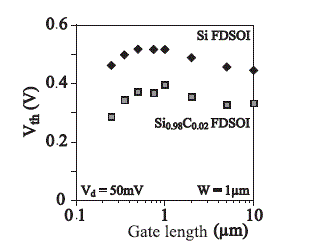
At the end of 2004, we demonstrated the beneficial effect of double Si/SiGeC diffusion barriers on the electric performances of very short gate length MOS transistors [DUC 04b]. For that, we selectively deposited in the Si windows of patterned, bulk Si(001) substrates with STI isolation (5 nm Si buffer/ Si0.88Ge0.12:C 10 nm / Si 5 nm / Si0.88Ge0.12:C 10 nm / Si channel 5 nm) stacks. These diffusion barriers make it possible to control the doping profiles in the Si channel, as well as in the source and drain zones (presence of 0.3% of C in the SiGeC layers). Regarding pMOS transistors, a reduced junction depth and a lower sheet resistance of the sources and drains are obtained, thanks to very retrograde B implantation profiles (presence of C atoms in interstitial sites). For nMOS transistors, we clearly highlighted that the presence of Si/SiGeC multilayer reduces the diffusion coming from the implanted B pockets, and thus short channel effects due to an over-doping of the channel. We have, moreover, integrated Si 10 nm/Si0.98C0.02 7 nm/Si 2 nm stacks right under the gate of fully-depleted silicon-on-insulator (FD-SOI) nMOS transistors with mesa-type isolation [DUC 06]. We will find in Figure 4.30 HR-TEM images of these transistors. These transistors show drain current Id — gate voltage Vg characteristics similar to those of reference Si FD-SOI transistors (see Figure 4.31). Si1-yCy curves are however shifted towards lower gate voltages than the Si ones. The Si1-yCy threshold voltage Vth reduction is about 0.13 ± 0.02 V, whatever the gate length (see Figure 4.32). However, we have seen above that the tensile strain in a Si1-yCy layer deposited on a Si substrate, generates a lowering of the conduction band edge by about 65 meV by percent of C atoms in substitutional sites. This Vth reduction is in very good agreement with the expected conduction band edge shift between Si0.98C0.02 and Si (no additional Vth shift is induced by doping, which is nonexistent in the channel of a FD-SOI transistor). This result clearly shows how interesting it is to use a Si1-yCy channel, to adjust the threshold voltage of nMOS FD-SOI transistors with a midgap metal gate (i.e. with a work function in the middle of the Si energy band gap). Threshold voltage tuning can then be done by varying the concentration in substitutional C atoms.
The same type of beneficial engineering of the threshold voltage (thanks to an adjustment of the alignment of the valence band between compressively-strained SiGe and Si) was highlighted in FD-SOI pMOS transistors with compressively-strained SiGe channels [AND 05b, HUT 10a]. Because of this Vth reduction, a gain of ~ 15% of the Ion on-state current was obtained in Si0.98C0.02 nMOS FD-SOI transistors with a gate length Lg = 0.35µm at Vg=Vd=1.2V.
Figure 4.30. HR-TEM images in cross-section of (from top to bottom) (i) a nMOS FD-SOI transistor with a Si/Si0.98C0.02/Si channel, (ii) the Poly-Si/TiN/SiO2 gate stack and (iii) the Si cap/Si0.98C0.02/Si (20 nm)/buried oxide stack
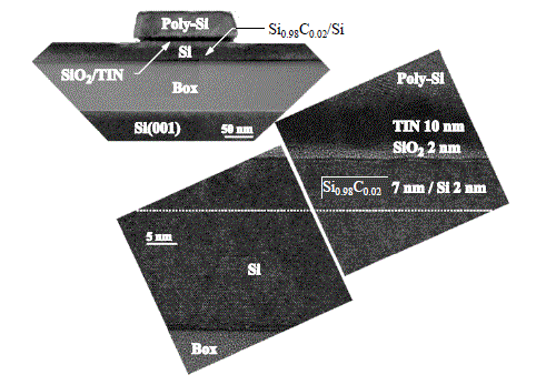
Figure 4.31. Id- Vg characteristics of a nMOS FD-SOI transistor with a Si0.98C0.02 channel and comparison with an FD-SOI device with Si reference channel (gate width = 0.2 µm, gate length = 0.35 µm)
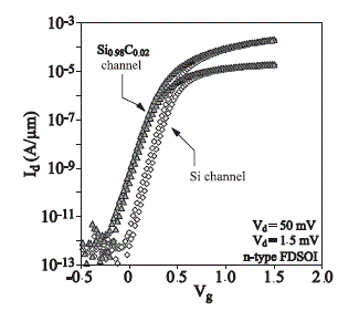
Figure 4.32. Threshold voltage according to the gate length illustrating the constant Vth shift between Si0.98C0.02 and reference Si FDSOI devices due to the conduction band edge discontinuity
4.4. Epitaxy of Si raised sources and drains on ultra-thin SOI substrates
4.4.1. Introduction
In the microelectronics industry, SOI substrates are increasingly used for the development of MOS transistors, because with them we can: (i) obtain very thin source/drain junctions, (ii) profit from low threshold voltages with low leakage currents (=> low voltage integrated circuits — low consumed powers), (iii) reduce the parasitic source-drain capacities for very powerful high frequency devices, but more energy-consuming, (iv) have circuits able to operate at high temperature, resistant to radiations, etc. However, the unceasing miniaturization in all dimensions of the components will require in the short term, to start from SOI substrates with much thinner Si and SiO2 layers (i.e. e(Si) < 10 nm and e(SiO2) < 100 nm), than those of the current commercial SOI substrates (e(Si) ~ 70 nm and e(SiO2) ~ 145 nm).
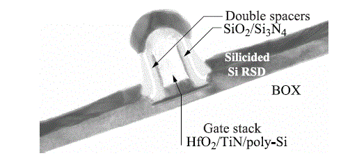
We will find in Figure 4.33 a cross-sectional TEM image in the proximity of the gate of a MOSFET transistor fabricated on an ultra-thin SOI substrate. Under the gate, the Si film is 8–10 nm thick only; however, for transistors architecture reasons, it is necessary to grow Si in a selective way with respect to SiO2 and Si3N4 (the isolation regions between individual transistors and the sidewall spacers, respectively) in the source and drains regions, in order to obtain in these zones final Si thicknesses of about 40 nm (for silicidation). We will then speak of Si raised sources/drains.
Figure 4.33. Cross-sectional TEM image of a MOS transistor fabricated on an ultra-thin SOI substrate. The Si channel under the gate has a thickness close to 10 nm, ~ 10 nm of Si (raised extensions) then ~ 20 nm of Si (raised sources and drains) have been deposited selectively in the source and drains regions, using an optimized growth process which is selective with respect to SiO2 and Si3N4 (see section 4.4.3 below)
It can also be interesting to grow a few nm of Si on blanket ultra-thin SOI substrates, in order to obtain SOI substrates with a slightly thicker upper layer, but with much lower surface roughness and macroscopic dispersion of thickness on the wafer surface, as shown in [HAR 03a].
4.4.2. Problems encountered on ultra-thin SOI substrates
With a conventional Si Selective Epitaxial Growth process [HAR 03a] (i.e. an ex-situ “HF-last” wet cleaning in an automated wet bench followed by an in situ H2 bake at 800°C for 2 minutes and a selective deposition of 40 nm of Si with a dichlorosilane + hydrochloric acid at temperatures typically around 800°C [MIY 99]) in the sources and drains regions of patterned, ultra-thin SOI wafers (i.e. Si thickness under the gate: 8–10 nm, in the sources and drains regions: 6–8 nm), we are confronted with two catastrophic problems for MOS transistors:
—Si withdrawal (i.e. “moat recess”) at the boundaries with the isolation oxide;
—Si film which loses its continuity, with the formation of islands.
Figure 4.34. Schematic representation and cross-sectional Scanning Electron Microscopy (SEM) images of the problems encountered with a conventional Si SEG process on an ultra-thin patterned SOI substrate (mesa isolation scheme): withdrawal (“moat recess”) at the boundaries of the active regions with the isolation oxide and agglomeration or islanding of the initially continuous Si film
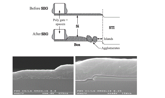
This Si agglomeration phenomenon on an ultra-thin SOI substrate has already been highlighted by Ono et al. [ONO 95] and by Ishikagawa et al. [ISH 02]. It occurs at increasingly lower temperatures, as the Si thickness reduces. In addition, going from a blanket to a patterned SOI substrate definitely decreases, at a given Si thickness, the temperature above which the Si layer becomes discontinuous with the formation of islands.
4.4.3. Method developed in response
In order to solve these “moat recess” and islanding problems, we have optimized the steps that follow [JAH 05]:
(i) in situ H2 bake before the Si growth
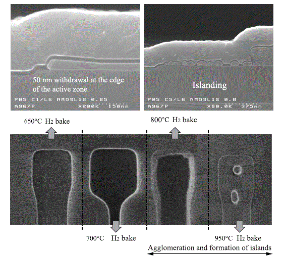
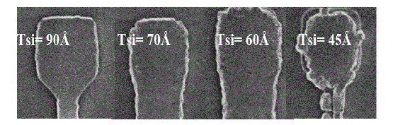
On these ultra-thin SOI substrates (thickness of the Si layer < 8 nm), we should use annealing temperatures lower than or equal to 700°C. Indeed, for temperatures higher than 700°C, there are indeed a withdrawal at the edge of the active zone and the formation of discontinuous islands, as illustrated in Figure 4.35.
Figure 4.35. Illustration of the effect of the H2 bake temperature on the morphology of an ultra-thin, patterned Si layer on BOX (here: 8 nm). For two minute bakes, we see that for temperatures higher than 700°C, we have a withdrawal of the film at the edges of isolated areas, then an agglomeration in islands
Using such H2 bake temperatures is in opposition to the way we usually proceed, in order to prepare a Si surface before epitaxy. Indeed, in order to get rid of any trace of residual contaminants (such as C, O or F atoms) on a “HF-last” Si surface, a few minutes in situ H2 bake at temperatures higher or equal to 775°C, must be used [HAR 03a]. Given that a perfect crystalline quality of Si or SiGe raised sources/drains is not essential for the technological steps used later on (i.e. ion implantation of dopants (usually As, B, P) making the layer amorphous followed by {recrystallization /electric activation of the dopants} spike anneals), some atomic contaminants at the {raised sources and drains / initial Si film} interface can be tolerated. Low temperatures H2 bakes guarantors of a good stability of the ultra-thin Si layers can thus be used prior to SEG.
(ii) Si selective epitaxial growth
Low growth temperatures (i.e. lower than or equal to 750°C) and a chlorinated chemistry (i.e. dichlorosilane + hydrochloric acid), which is selective with respect to SiO2 and Si3N4, should be used in order to thicken the Si area of ultra-thin (< 10 nm), patterned SOI wafers [HAR 04a]. We will find in Figure 4.36, an example of selective deposition of a 60 – 65 nm Si layer on an ultra-thin SOI substrate. For initial Si thicknesses of 6 nm and more, we have only little or almost no withdrawal at the edge of the active region, and no agglomeration. This method was intensively used in the last few years on standard FD-SOI electric lots, on FD-sSOI lots (with tensily-strained Si layers (see section 4.6)), on electric FD-SOI lots with not self-aligned double gates, etc. For more details concerning the obtained electrical properties, readers’ should refer to [AND 05b, AND 07, BAR 07, VIN 05].
Figure 4.36. Morphology of the Si layer after a 650°C, 2 minutes H2 bake followed by the SEG of 60–65 nm of Si at 750°C with a chlorinated chemistry (P = 20 Torr, F(SiH2Cl2)/F(H2) = 0.01, F(HCl)/F(H2) = 0.00208). We will note that for initial thicknesses of the Si film higher than or equal to 6 nm, we have no withdrawal or agglomeration
4.5. Epitaxy of recessed and raised SiGe:B sources and drains on ultra-thin SOI and SON substrates
4.5.1. Introduction
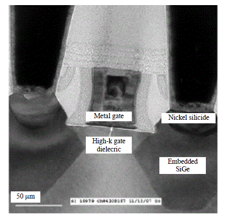
In order to boost the electrical performances of the pMOS transistors for the 65 nm and lower technological nodes, Intel proposed in 2003 to etch the sources and drains zones on both sides of the gate stack and to fill the cavities thus formed by in situ boron-doped SiGe. A uniaxial compressive stress is then induced (the SiGe lattice parameter is higher than the one of Si) in the Si channel for small gate lengths [ANG 05, COO 10, HUE 08, ZHA 06]. Outstanding electric performances are then obtained [HAN 06, MIS 07, THE 06, THO 06, YIN 06], justifying the adoption of this technology in production. As an example, we will find in Figure 4.37, a TEM image of a 45 nm technology node pMOS transistor of a Penryn Intel microprocessor [MIS 07].
Figure 4.37. Cross-sectional TEM image of a 45 nm technology node pMOS transistor. SiGe recessed sources and drains are present on both sides of the Si channel. The gate stack is of the “damascene” type with, as a gate dielectric, a SiON/HfO2 stack
From the epitaxy point of view, we are confronted with the following difficulties:
— surface preparation of the cavities prior to epitaxy;
— selective epitaxial growth (versus SiO2 and Si3N4) of several tens, or even of a hundred nm thick heavily in situ boron doped (~ a few 1020 cm-3) SiGe layers in those cavities. This might be troublesome as Ge concentrations have increased over the last few years from 20% to 35%. The appearance of defects due to plastic strain relaxation of these SiGe:B layers or at the locations where growth fronts coming from the edges of the cavities meet with the one at the bottom should be minimized or suppressed altogether.
We studied (given that our activities are centerd since 2004 on FD-SOI devices) the growth of:
— SiGe:B raised sources and drains on FD-SOI substrates and;
— recessed SiGe:B sources and drains on SON (silicon-on-nothing) substrates.
We will find below a few characteristics of the growth of SiGe:B layers on bulk, blanket Si(001) wafers, as well as morphological demonstrations of SiGe:B sources and drains on these two types of substrates.
4.5.2. Growth kinetics and boron doping of SiGe in chlorinated chemistry
We deposited thin, in situ boron doped SiGe layers on bulk, blanket Si(001) wafers slightly n-type doped (in order to have p-n junctions and thus to be able to carry out resistivity measurements) [HAR 04a, HAR 08a].
The strongly chlorinated growth chemistry used (SiH2Cl2 + GeH4 + B2H6 + HCl), as well as the chosen growth pressure (20 Torr), will enable us, during a transposition on patterned substrates, to be selective compared to SiO2 and Si3N4. The growth temperature was decreased from 700°C to 600°C, when switching from 20% to 50% of Ge, in order to remain pseudomorphic on Si and to have smooth surfaces for several tens of nm thickness.
We will find in Figure 4.38, resistivity curves associated with various Ge concentrations, 20–30 nm thick SiGe:B layers, according to the F(B2H6)/(F(SiH2Cl2)+F(GeH4)) mass-flow ratio.
Figure 4.38. Resistivity as a function of the F(B2H6)/(F(SiH2Cl2)+F(GeH4)) mass-flow ratio, for SiGe:B layers of various Ge concentrations (see figure insert)
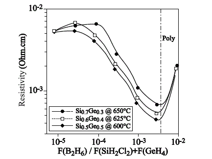
Figure 4.39. SiGe:B growth rates functions of the F(B2H6)/(F(SiH2Cl2)+F(GeH4)) mass-flow ratio, for various Ge concentrations (see figure insert: for values of %Ge and growth temperature)
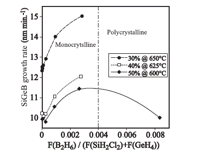
Figure 4.40. Apparent Ge concentration functions of the F(B2H6)/(F(SiH2Cl2)+F(GeH4)), for various SiGe:B layers (see insert of the figure: for values of %Ge and growth temperature)
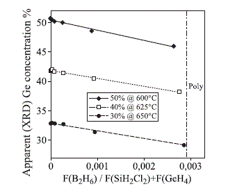
When the diborane flow increases, the resistivity decreases (as expected) up to values lower than 1 mOhm.cm. The minimums of resistivity of Figure 4.38 correspond to concentrations in B atoms between 2 and 3x1020 cm-3 [HAR 08a]. For more important diborane flows, SiGe:B layers become polycrystalline and rough. This explains the resistivity rise in Figure 4.38. We represented in Figures 4.39 and 4.40, the modifications induced by B doping for the growth rate and the “apparent” concentration in Ge (by supposing, during the fitting of the X-Ray Diffraction profiles that we have a binary SiGe alloy rather than a ternary SiGeB alloy). Although it is less obvious than in Si [GON 08, HAR 02a], we have a clear increase of the growth rate, related to the presence of B atoms on the surface, catalyzing at these low growth temperatures, the desorption of the H atoms, passivating the surface. The drop of the “apparent” concentration in Ge is due to high concentrations of B atoms (much smaller than those of Si or Ge [CHO 06]), inducing a contraction of the average SiGe:B lattice parameter (the real Ge content is rather steady).
4.5.3. Recessed and raised SiGe:B sources and drains on FD-SOI and SON substrates
We started from the data points described in section 4.5.2, in order to deposit at 650°C several tens of nm thick, heavily B doped Si0.7Ge0.3 raised sources and drains on both sides of FD-SOI transistors [HAR 08b]. We had to identify a trade-off between:
— in situ H2 bake (that follows the ex-situ “HF-last” wet cleaning) which had to be carried out at low temperature considering the thinness of the starting Si film;
— loading effects inherent to the growth on patterned substrates (see sections 4.2 and 4.3);
— decrease of the growth rate combined with a slight increase of the Ge concentration during any growth on SOI substrates [HAR 05b, HAR 09a].
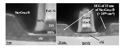
We will find in Figure 4.41 cross-sectional high-resolution TEM images of the sources and drains. We can notice on the right image, the excellent crystalline quality of the Si0.7Ge0.3:B layer, the presence of {111} facets, as well as the perfect growth selectivity, notably with respect to Si3N4 spacers. Given the very small quantity of SiGe under the level of the gate, we hardly expect to have holes mobility due to uniaxial compressive strain. However, efficient pMOS FD-SOI transistors have recently been obtained by IBM, thanks to the presence of faceted, raised SiGe sources and drains in situ B doped at very high levels (4 x 1020 cm-3), leading to a drastic reduction of the contact resistance possible [CHE 09a]. These raised SiGe:B sources and drains are certainly useful, when we wish to strongly decrease the thermal budget to which a technological stack is subjected (3D integration) [BAT 09a] or when there is a substrate with a lattice parameter larger than the one of Si (of the extra-strained SOI (section 4.6) or germanium-on-insulator type (section 4.7)).
Figure 4.41. High-resolution TEM images of raised Si0.7Ge0.3:B sources and drains with a 23 nm thickness selectively deposited on both sides of a FD-sSOI transistor
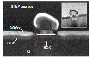
We used the same process to grow Si0.7Ge0.3: B recessed sources and drains on both sides of SON transistors (see section 4.8 for more details). We will find in Figure 4.42 cross-sectional TEM images of these structures. We find there the SON transistor, i.e. a conventional gate stack on the thin film of Si, itself separated from the Si substrate by a SiO2/Si3N4/SiO2 “sandwich”. On both sides of the latter, we notice the presence of a Si bridging that connects the channel to the source and drain zones. This bridging is topped by a SiGe:B layer, which was later on silicided with Ni. Although the sequence of process steps used is not yet optimum (presence of a definite mushroom of poly-SiGe on top of the gate due to the not controlled growth on poly-Si), we can clearly note that it is a configuration where SiGe on both sides could induce a uniaxial compressive stress in the thin Si channel, where the holes are propagating.
Figure 4.42. Cross-sectional TEM image of a SON transistor with recessed Si0.7Ge0.3:B sources and drains
To conclude this section, it is possible, thanks to Si1-yCy:P (y = 1.5 – 2%) recessed sources and drains with a lower lattice parameter than Si, to inject a uniaxial tensile strain in the Si channel of short gate length nMOSFETs transistors [BAU 07, GOU 09b, HUE 08]. Thanks to this strain, it is possible to significantly improve the electrons mobility and thus to obtain more efficient nMOSFETs transistors [YAN 08].
4.6. Virtual SiGe substrates: fabrication of sSOI substrates and of dual c-Ge / t-Si channels
4.6.1. Introduction
Biaxial tensily-strained Si layers (sSi or t-Si) grown pseudomorphically on virtual SiGe substrates are very interesting for high-efficiency CMOS devices. By SiGe virtual substrate, we mean a relatively thick SiGe layer deposited on a Si substrate, with a lattice parameter almost equal to that of a bulk SiGe substrate. There is indeed a significant increase in the electrons and holes mobility, due to the tensile strain in the Si layer. For electrons, the degeneracy of order 6 of the Δ valley of the conduction band, function of the directions <001>, is then lifted. The two valleys Δ2 perpendicular to the plane of the sSi layer go down then by 67 meV for each 10% increment of the Ge concentration in the SiGe virtual substrate, while the four in-plane valleys Δ2 go up by 67/2 = 33.5 meV each 10% increment of the Ge concentration (compared to un-strained Si) [MUN 08a]. The electrons’ inter-valleys scatterings are then reduced, as well as their effective mass. We notice experimentally an increase in the electrons mobility in sSi for Ge concentrations higher than 10%. This mobility gain saturates at 1.8 for concentrations higher than 20% [CUR 01].
Regarding the holes, the degeneracy of the valence band in the Γ center of the Brillouin zone is lifted by the tensile strain. The light holes band (which then goes up in energy) is then preferentially occupied compared to that of the heavy holes band. As for electrons, it generates a decrease of the inter-valley scattering and of the effective holes mass. We then obtain an increase in the holes mobility in sSi for Ge concentrations higher than 25%. This gain of holes mobility saturates at 2.2 for concentrations in Ge higher than or equal to 40% [LEI 02]. These modifications are schematized in Figure 4.43.
Figure 4.43. Schematic descriptions of the structural modifications generated by the epitaxy of a thin Si layer on a virtual SiGe substrate and their impact on the Δ valleys of the minimum of the conduction band and on heavy holes/light holes sub-bands of the valence band itself (because of the tensile strain)
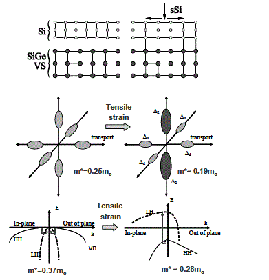
Because of the lower thermal conductivity of SiGe compared to Si (harmful for CMOS devices), it can prove to be extremely interesting to transfer these tensily-strained Si layers on oxidized Si substrates, thanks to the SmartCutTM method for the fabrication of sSOI or XsSOI substrates (as we will see in more detail further on). Such substrates, with a tensily-strained Si layer on an buried insulating layer, are helpful to obtain high performance fully-depleted SOI transistors [AND 05b, AND 06, AND 07, RIM 03].
4.6.2. Growth and structural properties of virtual SiGe substrates
Specifications as for virtual SiGe substrates grown on Si (001) substrates are as follows: (i) a SiGe layer on the surface almost completely relaxed (i.e. with a lattice parameter the closest possible to a massive SiGe crystal); (ii) a defect density in the aforementioned layer as low as possible; and (iii) a controlled surface roughness. In order to do that, we usually insert between the surface SiGe layer (of constant composition and with a thickness typically higher than one micron) and the Si substrate, a several microns thick SiGe layer with a linear ramp of concentration in Ge of several microns thickness (where the defects resulting from the accommodation to the difference in lattice parameter between SiGe and Si will be confined).
In the past, it was shown that it was interesting in CVD to use high growth temperatures (typically 800°C — 900°C), in order to obtain virtual SiGe substrates of good crystalline quality [CHU 98]. We thus started by studying the growth kinetics of SiGe at high temperatures with a SiH2Cl2 + GeH4 chemistry. Thanks to the chlorinated Si precursor, we should thus not clog the domes of the epitaxy chamber too much, despite the large thickness deposited. For that, we deposited several hundred nm thick, constant composition SiGe layers with Ge concentration discreetly increasing from one layer to another, separated with thin Si layers [BOG 05a, BOG 05b, BOG 06a, and HAR 06a]. We used X-Rays Diffraction (omega-2theta scans around the (004) and (224) orders) and Scanning Electron Microscopy, in order to determine the Ge concentration and the thickness (thus the associated growth rate) of each SiGe layer.
As an example, we will find in Figure 4.44, concentrations and growth rates obtained at 20 Torr and temperatures of 800°C, 850°C and 900°C. First of all, we will note that the Ge concentration increases in an almost linear way with the F(GeH4)/F (SiH2Cl2) mass-flow ratio. We used the simple relation proposed by Robbins et al. (describing the incorporation of Ge in silane chemistry [ROB 91]), in order to quantify the incorporation of Ge at high temperatures in dichlorosilane chemistry, i.e. x / (1-x) = m * F(GeH4) / F(SiH2Cl2). We found, as an example m(800°C) = 2.43, m(850°C) = 2.41 and m(900°C) = 2.16 for the variable GeH4 flow data points of Figure 4.44 (i.e. a Ge concentration decreasing when the temperature increases).
In the same way, we will see that the growth rate at these high temperatures is catalyzed only a little by the presence of Ge atoms on the surface (the fraction of surface sites which is passivated by H atoms is small). This is shown by a modest (800°C), even almost null (900°C) increase of the growth rate, when the GeH4 flux increases (with constant SiH2Cl2 flux).
Figure 4.44. Concentration in Ge (on the left) and growth rate (on the right) functions of the F(GeH4)/(F(SiH2Cl2) + F(GeH4)) mass-flow ratio (MFR), for: (i) a F(SiH2Cl2)/F(H2) MFR equal to 0.025 and a F(GeH4)/F(H2) MFR increasing from 4.17x10⁻⁵ up to 3.75x10⁻⁴ (open symbols) or (ii) a F(GeH4)/F(H2) MFR equal to 3.75x10⁻⁴ and a F(SiH2Cl2)/F(H2) MFR decreasing from 0.0025 to 0.00104 (full symbols). The growth temperature was equal to 800°C, 850°C or 900°C, while the growth pressure was equal to 20 Torr
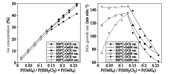
Thanks to these type of data points, we have been able to obtain virtual SiGe substrates of final concentration ranging between 20% and 50%. We will describe later on their main characteristics. In order to be exhaustive, we will however note that we have been able, on polished Si0.5Ge0.5 virtual substrates, to deposit, during a second epitaxy step, virtual SiGe substrates of final concentration between 55% and 100%. The interested reader can refer to [BOG 06a].
We will find in Figure 4.45, the SIMS profile of the Ge concentration of a virtual Si0.5Ge0.5 substrate. First of all, we deposited a layer with a Ge concentration increasing linearly from several % percent up to 50% (grading: ~ 9%Ge/μm), that we capped with a slightly more than one micron thick Si0.5Ge0.5 layer. A similar sample was pictured in TEM (see Figure 4.46). The 60° dislocations necessary to accommodate the lattice mismatch between SiGe and Si (glide planes: {111}) are very clearly restricted in the Ge concentration ramp.
No threading dislocation is visible (at least at the TEM local scale) in the constant composition SiGe layer on top.
Figure 4.45. SIMS profile of the Ge concentration in a Si0.5Ge0.5 virtual substrate
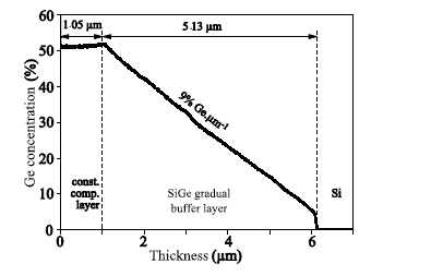
Figure 4.46. Bright field TEM image in the <110> direction of a Si0.5Ge0.5 virtual substrate. The misfit dislocations in the plane of the TEM sample appear in the form of light gray or white lines, while those perpendicular to that plane appear as points
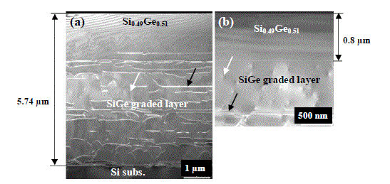
We used X-ray diffraction, in order to have access to the macroscopic degree of strain relaxation of the layer of constant composition defined as ![]() and
and ![]() are the in-plane and bulk (i.e. unstrained) lattice parameters of SiGe, while aSi = 5.43105 Å is the lattice parameter of the Si substrate. For more information on the protocol used, readers can refer to [BOG 05a]. We will find in Figure 4.47 the aforementioned macroscopic degree of strain relaxation functions of the germanium concentration of the constant composition layer, for relaxed substrates deposited at 850°C or 900°C.
are the in-plane and bulk (i.e. unstrained) lattice parameters of SiGe, while aSi = 5.43105 Å is the lattice parameter of the Si substrate. For more information on the protocol used, readers can refer to [BOG 05a]. We will find in Figure 4.47 the aforementioned macroscopic degree of strain relaxation functions of the germanium concentration of the constant composition layer, for relaxed substrates deposited at 850°C or 900°C.
Figure 4.47. Macroscopic degree of strain relaxation as a function of the germanium concentration of the constant composition layer
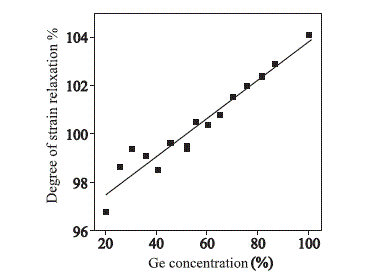
We can see that R increases in a monotonous way with the Ge concentration, going from values of about 96% for Si0.8Ge0.2 to 104% for a Ge virtual substrate. Values lower than 100% correspond to a residual strain in compression, while values higher than 100% mean than the layers are slightly tensily-strained. Such a train state could seem paradoxical at first glance (since we deposit on a substrate, a material with a higher lattice parameter). This is without counting with the coefficients of thermal expansion lower for Si than for SiGe [REE 96]. The high Ge concentration SiGe layers, almost completely relaxed at the epitaxy temperature (i.e. 850°C-900°C), see their in-plane lattice parameter shrinking with constants close of those of the Si substrates underneath (because of the epitaxy relationship). They are then slightly tensily-strained.
Because of the gliding on {111} planes of the threading arms of the misfit dislocations (whose intersections with a (001) surface are the [110] and [1–10] directions) and the periodic strain fields resulting from it [CHE 02, MER 10], we have on a SiGe virtual substrate the appearance of a “cross-hatch” surface structuring. There is indeed two perpendicular arrays of surface undulations along the <110> directions, with amplitudes that can be up to several tens of nm and with a spatial period between 1 and 3 μm. As an example, we will have in Figure 4.48, an AFM image of the surface of a Si0.5Ge0.5 virtual substrate. In Figure 4.49, we showed the surface root-mean-square (rms) roughness as well as the amplitude in z or “Z range” (= Zmax. — Zmin.), functions of the Ge concentration of the constant composition SiGe top layer, for virtual substrates deposited at 850°C or 900°C. We can notice that the rms roughness, between 2 and 3 nm for 20%-30% of Ge, significantly increases for higher concentrations, with values of about 10 nm for 50% of Ge.
Figure 4.48. Tapping mode AFM image of the surface of a Si0.5Ge0.5 virtual substrate. Image edges are approximately along the <100> directions
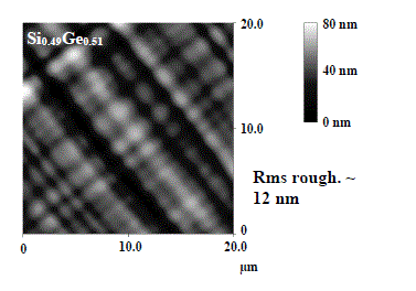
Figure 4.49. RMS roughness and Z range (deduced from 20 µm x 20 µm AFM images of the surface of SiGe virtual substrates) according to the Ge concentration of the constant composition SiGe layer sitting on top
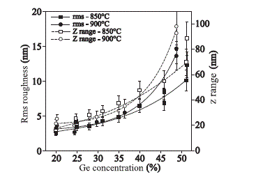
We can however get rid of this surface roughness using chemical mechanical polishing (removal of approximately 0.5 µm of SiGe), followed by dedicated wet cleaning ([ABB 06, ABB 08]). We then obtain “cross-hatch”-free surfaces, with rms roughness of about 0.4 nm.
In order to conclude the characterization of these virtual substrates, the threading dislocations density in the constant composition SiGe layers on top remains to be evaluated. Those threading dislocations (either isolated from one another, called thereafter “field”, or in pile-ups) will indeed be present in layers subsequently grown on top of our polished SiGe virtual substrates (for example, tensily-strained Si layers). We can either use standard Secco or Schimmel chemical solutions [ABB 07a], or profit from the fact that we have gaseous HCl in our epitaxy reactors [BOG 05c], in order: (i) to decorate the threading arms (creation of etching pits) and (ii) determine their density using optical microscopy. We will find in Figure 4.50, surface images of a Si0.5Ge0.5 virtual substrate, after HCl decoration of the threading dislocations.
Figure 4.50. 260 µm x 195 µm bright field optical microscopy images of the surface of a Si0.54Ge0.46 virtual substrate after HCl decoration of the defects. The images were acquired along the wafer radius. The distance to the center of the 200 mm Si(001) substrate is indicated for each image, as well as the density of threading dislocations
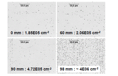
We will note that the density of threading dislocations is relatively constant up to the three-quarters of the wafer radius, with almost no piled-up threading dislocations. However, the density increases significantly when we approach the wafer edge. There are indeed values 20 times higher (4x10⁶<=> 2x105 cm-2) 2 mm from the edge and the presence of pile-ups.
We will find in Figure 4.51, the evolution of the threading dislocation density (isolated as well as in pile-ups) close to the wafer center, depending on: (i) the growth temperature for virtual Si0. 8Ge0.2 substrates and (ii) the Ge concentration of the constant composition layer (between 20% and 50%), for growth temperatures of 850°C and 900°C.
Increasing the growth temperature from 750°C to 950°C led to dramatically decreasing, for Si0.8Ge0.2, the density of threading dislocations. Moreover, we have values increasing monotonously from 105 to 2x105 cm-2, by going from 20% to 50% of Ge (at 900°C). Increasing the growth temperature further would however not allow us to drastically gain in terms of densities.
For temperatures higher than 900°C, we have indeed noticed that the surface became rougher, inhibiting the propagation of the threading arms of misfit dislocations to the wafer edges and their mutual elimination.
The data in Figure 4.51 was obtained for R%Ge/µm concentration gradients in the gradual layer between 8% and 10%. However, it was shown that the density of threading dislocations ρ was partly predicted by the following relation: ![]() GR being the growth rate of these virtual substrates, T the growth temperature and Ea a characteristic energy of the decrease of the dislocations density when the growth temperature increases [FIT 99, LEI 01]. We found the Ea value to be 1.43eV (see Figure 4.51), i.e. a value very close to the one found in the literature (1.38 eV) [LEI 01]. This relation was partly verified for Si0.8Ge0.2 virtual substrates. A threading dislocations density of 6 x 104 cm-2 only was obtained for 4% of Ge/µm and a growth rate of 140 nm min-1.
GR being the growth rate of these virtual substrates, T the growth temperature and Ea a characteristic energy of the decrease of the dislocations density when the growth temperature increases [FIT 99, LEI 01]. We found the Ea value to be 1.43eV (see Figure 4.51), i.e. a value very close to the one found in the literature (1.38 eV) [LEI 01]. This relation was partly verified for Si0.8Ge0.2 virtual substrates. A threading dislocations density of 6 x 104 cm-2 only was obtained for 4% of Ge/µm and a growth rate of 140 nm min-1.
Figure 4.51. Densities of threading dislocations present in (a) Si0.8Ge0.2 virtual substrates deposited at various temperatures and (b) SiGe virtual substrates of final concentration ranging between 20% and 50% deposited at 900°C
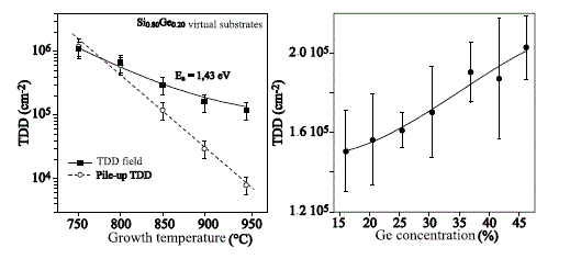
Such a value is at the state of the art for Si0.8Ge0.2 virtual substrates (7 x 104 cm-2 [WES 04] and 4.5 x 104 cm-2 [ERD 05]). Reducing the Ge concentration gradient and thus thickening the gradual layer is however quickly limited, when switching to SiGe virtual substrates with a Ge concentration higher than 20% (because of the convex shape of the wafer and the prohibitive growth time).
4.6.3. Growth and structural properties of tensily-strained Si layers on SiGe virtual substrates
We have studied the epitaxial regrowth of thin, tensily-strained Si (sSi) layers on our polished SiGe virtual substrates. It is indeed critical to check that they are smooth, of good crystalline quality (i.e. no multiplication of the defects compared to the virtual substrates underneath), really tensily-strained, etc. We will describe here the main features of the sSi layers deposited at 700°C with dichlorosilane on SiGe virtual substrates with Ge concentrations ranging between 20% and 50%, this after a “HF-last” wet cleaning, followed by a H2 bake at 850°C for two minutes. [HAR 07b, HAR 07c, HAR 08c]. We will let the reader take note in [HAR 08d] of the impact of the in situ H2 bake conditions on the properties of sSi layers on Si0.7Ge0.3 and Si0.6Ge0.4.
Figure 4.52. High-resolution TEM image (on the left) and SIMS depth profiles of the Ge concentration (on the right) for 37 nm thick Si layers deposited on Si0.8Ge0.2 and Si0.7Ge0.3 virtual substrates
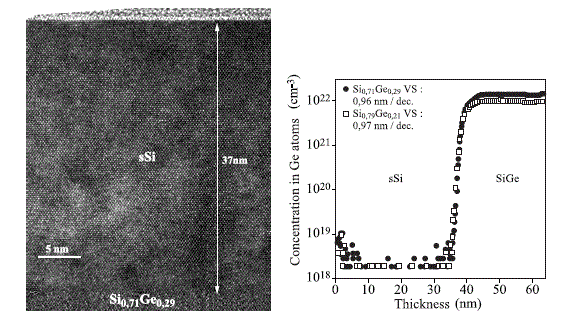
We will find in Figure 4.52, a cross-sectional TEM image of a 37 nm thick sSi layer deposited on a polished Si0.7Ge0.3 virtual substrate. This layer is locally of great crystalline quality, as proved by the presence of well-ordered {111} inclined planes and the absence of extended defects. We will also find in Figure 4.52 a SIMS profile of the Ge atoms in 37 nm thick sSi layers deposited on polished Si0.8Ge0.2 and Si0.7Ge0.3 virtual substrates. The interface between sSi and SiGe is abrupt, as proved by the interface Ge concentration decay: between 0.7 and 1.1 nm/decade for Ge concentrations between 20% and 50%.
We will find in Figure 4.53, an AFM image of the surface of a 37 nm thick tensily-strained Si layer deposited on a polished Si0.7Ge0.3 virtual substrate. We will note that except a small reappearance of the “cross-hatch”, related to the presence of periodic, tensile strain fluctuations in Si (see UV-Raman cartographies in [MER 10, ROU 08]), the surface remains smooth.
We have indeed obtained rms roughness ranging between 0.3 and 0.4 nm, this almost independently from the thickness of the tensily-strained Si layer or from the Ge concentration of the polished SiGe virtual substrate underneath.
We used Raman ultraviolet spectroscopy, in order to quantify the tensile strain in our sSi layers. We will see in Figure 4.54, that the strain almost does not depend on the thickness of the sSi layers. The stress levels, 1.32, 1.87, 2.58 and 3.15 GPa for sSi on Si0.8Ge0.2, Si0.7Ge0.3, Si0.6Ge0.4 and Si0.5Ge0.5, are close to those theoretically expected for completely pseudomorphic sSi layers. Similar strain values have been obtained thanks to the Geometric Phase Analysis (GPA) of high-resolution cross-sectional TEM images of these samples [HUE 07].
Figure 4.53. Tapping mode, 10 µm x 10 µm AFM image of the surface of a 37 nm thick sSi layer on a polished Si0.7Ge0.3 virtual substrate. Image sides are approximately along the <100> directions
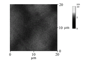
We also studied and quantified the defects found in these sSi layers, because of their epitaxy on dislocated SiGe virtual substrates. We will find in Figure 4.55, a plane view TEM image of a 37 nm thick sSi layer on a polished Si0.7Ge0.3 virtual substrate and in Figure 4.56, an optical microscopy image of the same sample, after a Secco revelation of the defects in the sSi layer.
Figure 4.54. Tensile strain (GPa), functions of the thickness of the sSi layers grown on polished SiGe virtual substrates for various Ge concentrations
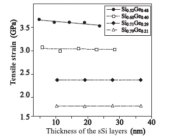
Figure 4.55. Plane-view TEM image of a 37 nm thick sSi layer on a polished Si0.7Ge0.3 virtual substrate
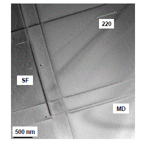
In Figure 4.56, we can notice the presence: (i) of white dots (characteristic of the presence of threading dislocations) and (ii) of lines along the <110> directions. Those are most likely due to the presence of stacking faults (in the whole sSi layer) or in-plane segments of misfit dislocations (at the sSi/SiGe interface). We expect indeed that the 60° misfit dislocations present in the SiGe virtual substrate underneath dissociate themselves (because of the tensile strain in the sSi layer) in partial 30° and 90° dislocations, propagating at different speeds in sSi, leaving in their wake stacking faults, as illustrated in Figure 4.55 [BED 04, HIR 05, KIM 06]. These stacking faults are more deleterious from the electrical transport point of view [YAN 00], than the in-plane segments (at the sSi/SiGe interface) of 60° misfit dislocations (although these act as dopant diffusion channels in bulk nMOS transistors [FIO 04]).
Figure 4.56. Optical microscopy image of the surface of a 37 nm thick sSi layer on a polished Si0.7Ge0.3 virtual substrate after the Secco etching of the totality of the sSi layer and of a few nm of the SiGe layer underneath
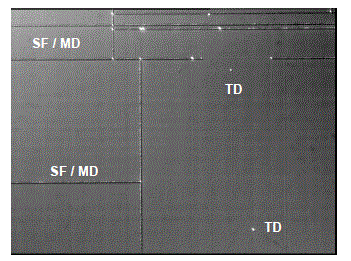
After Secco defect decoration, we quantified the surface density of threading dislocations (see Figure 4.57) and the linear density of <110> extended defects (see Figure 4.58), functions of the sSi thickness and of the concentration in Ge of the virtual substrate. The density of threading dislocations is close to that of virtual SiGe substrates. It increases only a little (from ~ 105 to 3x105 cm-2) when the sSi layer thickness increases.
The linear density of extended defects, almost null for thicknesses lower than 10 nm, monotonously increases with the sSi thickness, reaching values as high as 800 cm-1. It seems that this linear density depends not only on the Ge concentration (the higher the concentration is, the higher the linear density will be), but also on the flatness of the polished virtual SiGe substrate [HAR 07c, HAR 08b].
Figure 4.57. Surface density of threading dislocations according to the thickness of sSi layers deposited on polished SiGe virtual substrates (of %Ge between 20% and 50%)
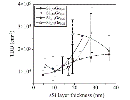
Figure 4.58. Linear density of <110> extended defects, according to the thickness of sSi layers deposited on polished SiGe virtual substrates (of %Ge between 20% and 50%)
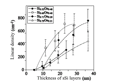
As a conclusion, we highlighted that it was possible to obtain pseudomorphic sSi layers on SiGe for thicknesses more important than those expected (by reversing of course the sign of the strain), according to the plastic relaxation curves of compressively-strained SiGe on Si (see Figure 4.9 of section 4.1). We will then speak about supercritical sSi layers, which have recently been inserted in “bulk” [FIO 04, SUG 05] or partially depleted-sSOI [COL 06, THE 05a, THE 05b, THE 06, YIN 06] transistor lots, with excellent electric properties.
4.6.4. Fabrication of sSOI and XsSOI substrates & transport properties
sSi layers on SiGe virtual substrates can be transferred thanks to the SmartcutTM technology on oxidized Si substrates. We thus obtain substrates, known as strained SOI [GHY 04] (when Si was tensily-strained on Si0.8Ge0.2) or as eXtra-strained SOI [AKA 06a] (when Si was tensily-strained on SiGe with [Ge] > 20%).
We will find in Figure 4.59, the main process steps leading to the fabrication of these structures. After deposition of a SiGe virtual substrate that we polish, we deposit a thin sSi layer (see sections 4.6.2 and 4.6.3), that we encapsulate by several tens of nm of SiO2, deposited at a reduced temperature. We carry out a H+ ion implantation (high dose and implantation energy). Then, we bond the aforementioned stack on an oxidized Si substrate. Annealing leads to the agglomeration of hydrogen atoms in planar cavities, thus creating a zone of mechanical fragility, which is put to good use for the fracture. We find ourselves then with a rough SiGe layer on sSi, itself on a buried oxide. We then use a selective chemical etching, to remove the remaining SiGe, while stopping on sSi. We then obtain sSOI or XsSOI substrates which are locally of excellent crystalline quality (see Figure 4.59) and whose bonding interface has been strengthened thanks to suitable annealing [BOG 06b].
We have been able to check, thanks to UV-Raman measurements that the sSi layer kept its tensile strain [MUN 08a, ROU 08]. HCl and Secco defect revelations showed that the threading dislocations were not multiplied during the use of the SmartcutTM process [ABB 07b]. Moreover, we called upon Hall effect [BOG 04, HAR 04c] and photoluminescence measurements at 3–9K [BOU 04, MUN 08a, MUN 08b], in order to check the electronic quality of our tensily-strained Si layers. Those were either: (i) inserted in SiGe in the proximity of an in situ phosphorous-doped SiGe layer used as an electron reservoir (structures known as “MODFETs” [BOG 04, BOU 04, HAR 04c]) or (ii) directly on buried oxide with a thin high temperature oxide layer over it (in order to confine the charge carriers and suppress non-radiative surface recombination) [MUN 08a, MUN 08b].
Figure 4.59. (a) Main process steps in order to obtain sSOI or XsSOI substrates. (b) Cross-sectional TEM images of a 8 nm thick XsSOI 40% substrate
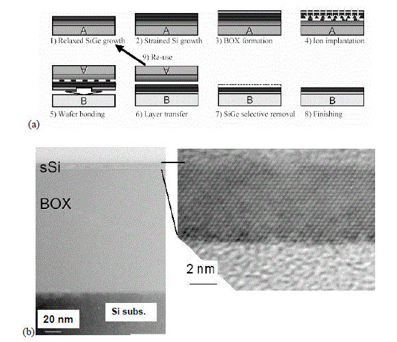
We have been able to confirm (thanks to Shubnikov-De Haas oscillations of the longitudinal resistivity and to the Hall plateaux of the transverse resistivity) the presence at liquid helium temperature of 2D electron gases in MODFETs structures. The mobilities obtained (212,000 cm2 V-1 s-1 for a 5.4x1011 cm-2 electrons sheet density) are comparable to those obtained using dedicated tools in academic laboratories. In the same way, we have been able to clearly highlight the presence in photoluminescence of NP and TO lines, related to the radiative combination, assisted by phonons (TO) or not (NP) of electron-hole pairs in sSi layers. Their energy position depends not only on the value of the tensile strain [MUN 08a], but also on the sSi layer thickness [MUN 08b].
We thus used those 1.3 GPa sSOI and 1.9 GPa XsSOI substrates (sSi on Si0.8Ge0.2 and sSi on Si0.7Ge0.3, respectively) to obtain high- performance FD-SOI nMOS and pMOS transistors [AND 05b, AND 06, AND 07]. We will find in Figure 4.60, a TEM image of one of the short gate length transistors, and in Figure 4.61, the obtained carrier mobilities (for long transistors). As expected, we have an electron mobility gain by a factor of 2. The gain is however much more modest regarding the mobility of the holes: +10% by going from SOI to XsSOI substrates.
Figure 4.60. Cross-sectional TEM image of a short gate length (25 nm) FD-sSOI transistor
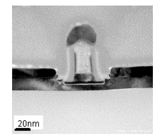
An elegant CMOS integration solution would then be to start from patterned sSOI substrates and to selectively deposit {compressively-strained SiGe / thin Si cap} bi-layers on the pMOS active areas. With that, we would gain simultaneously in electron and hole mobilities, this on the same wafer. We will see in Figure 4.62, a short gate length pMOS transistor fabricated on a sSOI substrate with a 20 nm thick Si0.6Ge0.4 channel for the holes capped with a few nm of sSi (in order to have a good electrical quality gate dielectric).
Changing the material and the strain state of the channel (c-SiGe instead of sSi) is extremely beneficial for the holes mobility, as illustrated in Figure 4.63: it is indeed multiplied by two!
Given the obtained hole mobility gains, we could push the reasoning a little further and move over to pMOS transistors with, as conduction channels, highly compressively strained Ge layers. That is what has been done, as shown in section 4.6.5..
Figure 4.61. Effective mobility of the electrons and holes, according to the inversion charge density in conventional SOI, sSOI and XsSOI substrates
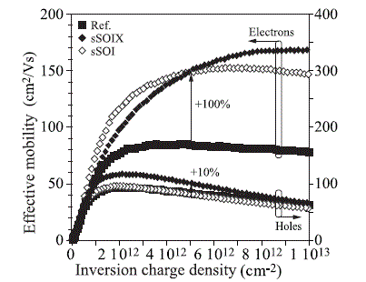
Figure 4.62. Cross-sectional TEM image of a pMOS transistor on sSOI with, as the conduction channel for the holes, a Si0.6Ge0.4 layer
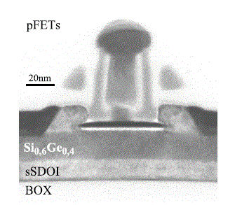
Figure 4.63. Effective hole mobility functions of the inversion charge density in conventional SOI substrates, sSOI substrates and BOX/sSi/Si0.6Ge0.4/sSi stacks (known as dual channel on insulator — DCOI)
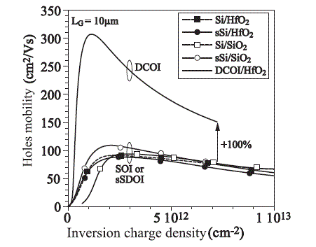
4.6.5. c-Ge/t-Si dual channels on Si0.5Ge0.5 virtual substrates
We started from polished Si0.5Ge0.5 virtual substrates, in order to make symmetrical — as much as possible — the strain in the {compressively-strained Ge / tensily-strained Si (noted hereafter c-Ge / t-Si)} dual channels that we wish to have. Given the thicknesses aimed for (c-Ge: ~ 8 nm, t-Si: ~ 5 nm), it seemed vital to (in agreement with literature [LEE 04]):
(i) significantly lower the epitaxy temperature of the c-Ge layer and not to exceed 8–9 nm, in order to avoid any elastic (undulations) or plastic (misfit dislocations) relaxation of the compressive stress;
(ii) optimize the Si encapsulation process of this Ge layer.
The deposition temperature of the c-Ge layer, using GeH4, 350°C, is close to the lower detection and piloting limit of our infra-red pyrometers (~ 330°C). We nevertheless obtain a growth rate of about 2.8 nm min.-1. As for its encapsulation by Si, we first of all carried out a Si passivation of the c-Ge layer at 350°C with SiH2Cl2 chemistry (the growth rate, initially non-null because of the presence of Ge atoms on the surface, becomes non-existent as soon as the surface is entirely covered with Si atoms, i.e. after ~ 5 Å of deposition). Then, we slowly go (1°C/s) under SiH2Cl2 up to 650°C, temperature at which we thickened the aforementioned t-Si layer (growth rate: ~ 0.5 nm min.-1) [BOG 05d].
Figure 4.64. (On the left) dark field and (on the right) high-resolution cross-sectional TEM images of a c-Ge/t-Si dual channel on a Si0.5Ge0.5 virtual substrate
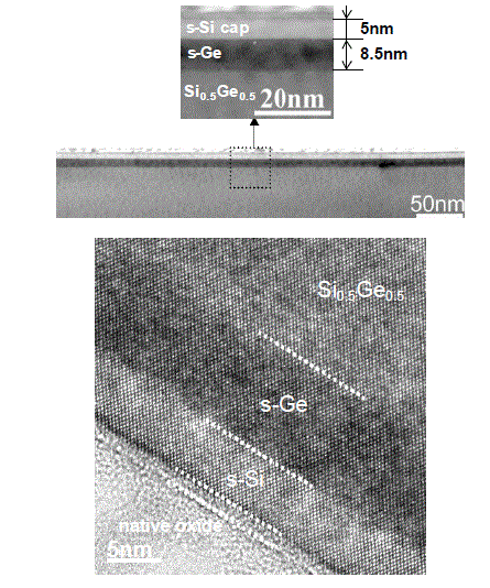
We can note in Figure 4.64, the planarity of the surface and of the interfaces, as well as the absence of extended defects. We checked, thanks once again to the Geometric Phase Analysis of high-resolution TEM images, that these Ge and Si layers were indeed pseudomorphic on Si0.5Ge0.5, with the expected levels of compressive and tensile strains [CHE 06].
We thus proceeded with the integration of these dual channels in pMOS transistors and of tensily strained Si layers in nMOS transistors, the dimensions of the devices being relaxed and the integration scheme being simplified [WEB 05]. We will find in Figure 4.65 cross-sectional TEM images of one of these dual channel transistors. The interface between t-Si and c-Ge is well defined and abrupt, just as those of the HfO2/TiN/Poly-Si gate stack. We showed in Figure 4.66, the mobility of charge carriers (electrons in Si or t-Si, holes in Si or in c-Ge/t-Si). As observed before with this type of gate stack, there is a drop in the un-strained Si of the mobility, compared to the universal mobility in bulk Si.
Figure 4.65. Cross-sectional TEM images of a pMOS transistor on a c-Ge/t-Si dual channel
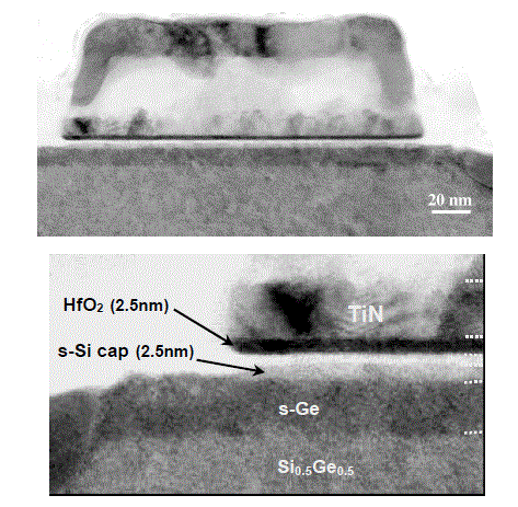
As expected, we find a gain of 65% of the electrons mobility in t-Si. The mobility gain of the holes is however extremely high: a factor of 9! Thanks to this gain, we can balance the on-state characteristics of nMOS and pMOS transistors, as illustrated in Figure 4.67. We will however note that the ION/IOFF (on-state current/off-state current) compromise is only 103 in this type of stacking, a value much lower than the one usually obtained for Si transistors (likely due to band-gap lowering in compressively strained Ge).
Figure 4.66. Mobility of the charge carriers in: (i) bulk Si, (ii) tensily-strained Si and (iii) a c-Ge/t-Si dual channel, functions of the effective field
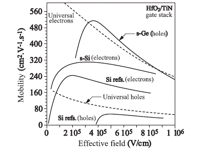
Figure 4.67. On-state drain current functions of the gate overdrive VG-VTH (threshold voltage) in: (i) bulk Si, (ii) tensily-strained Si and (iii) a c-Ge / t-Si dual channel
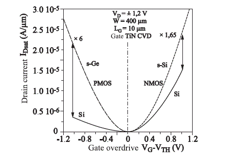
4.7. Thin or thick layers of pure Ge on Si for nano and opto-electronics
4.7.1. Introduction
Thin or thick Ge layers deposited on Si are very interesting because of their intrinsic properties. First of all, the energy band gap of Ge is much lower than the one of Si (Eg (Ge) = 0.67 eV ![]() Eg (Si) = 1.11 eV at room temperature). This allows its use as a light emitting or detecting material in the near infra-red, i.e. at the wavelengths used in optical waveguides (1.3–1.55 µm). We will favour pseudomorphic heterostructures such as multiple planes of Ge quantum dots in Si for electroluminescence [BRU 00, DAM 04b, HAR 05c]. Several hundreds of nm thick pure Ge layers selectively grown in Si cavities at the end of optical waveguide (see Figure 4.68) lead to the efficient conversion of a light signal into electric impulses (i.e. light detection) [HAR 04d, HAR 04e, OSM 09, ROU 06, VIV 07, VIV 09].
Eg (Si) = 1.11 eV at room temperature). This allows its use as a light emitting or detecting material in the near infra-red, i.e. at the wavelengths used in optical waveguides (1.3–1.55 µm). We will favour pseudomorphic heterostructures such as multiple planes of Ge quantum dots in Si for electroluminescence [BRU 00, DAM 04b, HAR 05c]. Several hundreds of nm thick pure Ge layers selectively grown in Si cavities at the end of optical waveguide (see Figure 4.68) lead to the efficient conversion of a light signal into electric impulses (i.e. light detection) [HAR 04d, HAR 04e, OSM 09, ROU 06, VIV 07, VIV 09].
Multiple planes of Ge quantum dots in Si or high Ge concentration Si/SiGe superlattices can also act as active material for photo- detection in these domains of wavelength, with however a lesser absorption efficiency [KUR 02a, KUR 02b, MAS 03].
Moreover, we can take advantage from the fact that the lattice parameter of GaAs (sphalerite structure) is very close to the one of Ge (aGe = 5.65785 Å ![]() aGaAs = 5.6533 Å) to deposit GaAs-based heterostructures such as solar cells [AND 05a], laser diodes [KWO 06], bipolar or high electronic mobility transistors [LIU 09, LUB 08], etc., on Ge (see Figure 4.68). In that case, vicinal surfaces (typically misorientated by 6° in one of the <110> directions) will be used, so that there are biatomic steps on the surface and thus to minimize the appearance of anti-phase boundaries harmful to the electronic properties of active structures [HAR 09b, TAN 06].
aGaAs = 5.6533 Å) to deposit GaAs-based heterostructures such as solar cells [AND 05a], laser diodes [KWO 06], bipolar or high electronic mobility transistors [LIU 09, LUB 08], etc., on Ge (see Figure 4.68). In that case, vicinal surfaces (typically misorientated by 6° in one of the <110> directions) will be used, so that there are biatomic steps on the surface and thus to minimize the appearance of anti-phase boundaries harmful to the electronic properties of active structures [HAR 09b, TAN 06].
With a low electric field, electrons and holes mobilities in bulk Ge are respectively twice and four times higher than those in Si (see Figure 4.68). Significant gains in performances are thus expected in MOSFETs transistors fabricated on Ge, provided that there is an efficient gate stack (with, as a gate dielectric, a high-K material such as HfO2 (considering the strong instability of Ge oxide)). GeOI (Ge-on-insulator) substrates fabricated thanks to the SmartCutTM process with as donor wafers bulk Ge substrates or thick Ge layers on Si [AKA 06b, AUG 09, CLA 06] lead to a better electrostatic control (i.e. less short channel effects, smaller junctions capacities, etc.). A gain of a factor of 2 of the holes mobility was evidenced in pMOSFETs transistors on GeOI, as we will see later on [POU 08, POU 09, ROY 08, VIN 10].
Figure 4.68. Schematic description of a Ge photo-detector on SOI; (on the top left) energy band gap functions of the sphalerite lattice parameter for various II-VI, III-V and IV-IV semiconductors; (on the bottom left) charge carriers velocity functions of the electric field in Si, Ge and GaAs
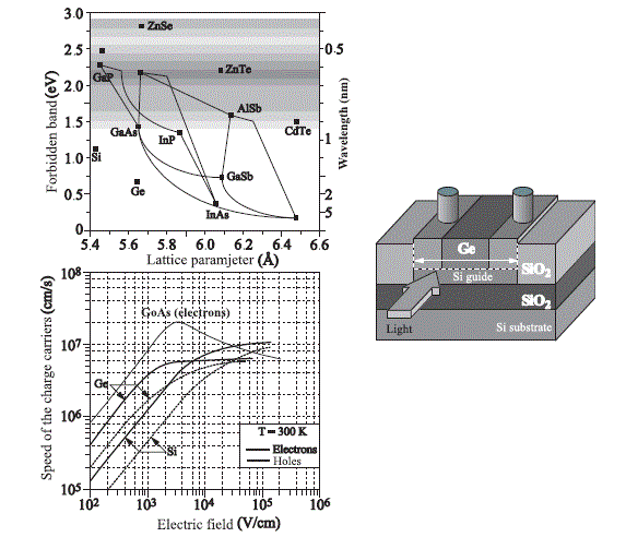
In the following sections, we will focus: (i) on the structural properties of thick Ge layers grown on Si(001) and of the GeOI substrates resulting from it, (ii) on the electric properties of pMOSFETs transistors fabricated on GeOI and of near-infra red photo-detectors based on pure Ge and (iii) on the growth and optical properties of Ge quantum dots inserted in Si.
4.7.2. Structural properties of thick layers of Ge on Si (001) and of GeOI
It is difficult, because of the important discrepancy of the lattice parameter (4.2%), to obtain on Si(001), Ge layers with the sought properties, i.e. a flatness compatible with advanced lithography or layer transfer process steps, a defect density minimized for efficient devices, etc. Several different approaches can lead to such films. Ge virtual substrates (i.e. with a Ge concentration grading from 0% to 100% in ~ 10 μm) are characterized by a macroscopic degree of strain relaxation slightly higher than 100% and a rather low threading dislocations density (~ 106 cm-2). They are nevertheless rough (appearance of a strong cross-hatch) [BOG 06a, CUR 98, THO 03] and, in the case of a deposition on one face only of the Si substrate, severely bowed (bow of about 250 μm) [HAR 10a]. Chemical Mechanical Polishing is then mandatory, in order to recover a smooth surface. The approach thus chosen was proposed in 1998 by Colace et al. [COL 98], closely followed by Hernandez et al. [HER 03]. It consists of depositing at low-temperature a thin Ge “seed” layer, followed by the deposition at high temperature of a thick Ge layer [EAG 91, HAR 04d, HAR 04e, HAR 05d, HAR 08e, HAR 09b, LUA 99, SAK 97]. The low temperature (330°C-400°C) chosen for the first Ge layer leads to a nearly complete plastic relaxation of the elastic stresses stored without too many surface undulations. The high temperature (600°C-850°C) used to deposit the second Ge layer leads to a drastic drop in the density of threading dislocations, as well as a reduction of the growth time. Later on, we can use a thermal cycling (typically between 750°C and 875–900°C), in order to further reduce the density of crystalline defects (thanks to the thermally assisted propagation of the threading arms of misfit dislocations, their mutual annihilation and their elimination at the edge of the substrate) [HAR 04d, HAR 05e, HAR 09b, LUA 99]. Such a method is however time consuming (although a recent study showed that a reduced number of short cycles gave the same densities of emergent defects as long cycles in greater number [HAR 10b]).
From the growth protocol point of view, we proceeded as follows. First of all, we deposited on Si(001) 130 nm of Ge at low-temperature (400°C) and at a pressure of 100 Torr, in order to profit from a relatively high growth rate: 14 nm min.-1 for a F(GeH4)/F(H2) mass-flow ratio equal to 7.917 x 10⁻⁴ [HAR 08e].We then slowly ramped-up the temperature under GeH4 from 400°C to 750°C (1°C/s), while reducing the pressure from 100 Torr to 20 Torr.~ 85 nm of Ge is deposited during this ramp. We then thickened this Ge layer at 750°C, 20 Torr, with the same F(GeH4)/F(H2) mass-flow ratio as previously (growth rate: 47 nm min.-1). The following thermal cycling: 890°C, 5 min + 3x{750°C, 5 min/890°C, 5 min} can be implemented on those thick Ge layers (2570 nm here),so as to minimize the threading dislocations density.
We will find in Figure 4.69 AFM images of the surface of these Ge layers functions of the thickness deposited. Just after the growth of the 130 nm of Ge at 400°C, the surface is rather rough, with low spatial wavelength undulations (a few hundred nm). After the temperature rise up to 750°C under germane, these undulations coalesced, giving rise to higher spatial wavelength undulations (~ 1 μm). These undulations continue to stretch in the growth plane during the thickening at 750°C (images corresponding to 1,395 and 2,570 nm of deposited Ge). For such layers, the surface has a morphology which a mix between low amplitude “hills” and a “cross-hatch”, i.e. an array of undulations along the <110> directions, as for SiGe virtual substrates. There is otherwise the presence of “hills” flanks of large terraces separated from one another by bi-atomic steps [HAR 10b]. The subsequent use of a thermal cycling leads to a surface morphology closer to the one of SiGe virtual substrates, i.e. a “cross-hatch” defined better at the expense of the “hills”.
Figure 4.69. Tapping mode AFM images of the surface of Ge layers deposited on Si(001), for ~ 130 nm of Ge at 400°C, a 130 nm thick Ge “seed layer” at 400°C + 85 nm of Ge deposited during the temperature ramping-up from 400°C to 750°C (215 nm), after the thickening of this layer with either 1180 or 2355 nm of Ge at 750°C (1395 and 2570 nm), and after thermal cycling of a 2570 nm thick Ge layer
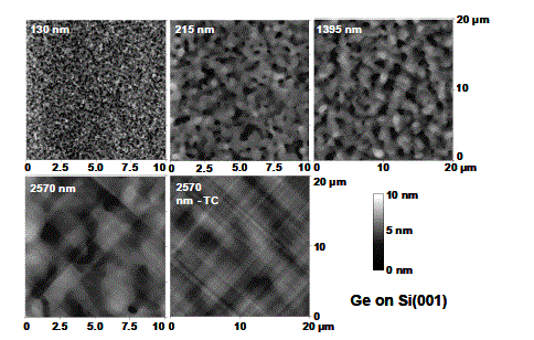
In Figure 4.70, we showed the evolution of the surface rms roughness and Z range (i.e. Zmax. − Zmin.), functions of the thickness of the Ge layer deposited on Si(001). A monotonous decrease of these two parameters is clearly highlighted, as soon as we thicken at 750°C the Ge “seed” layer deposited at 400°C. Surface rms roughness and Z ranges of about 0.7 nm and 4.5 nm are obtained for 2.5 µm thick Ge layers, thermally cycled or not. Although these values are remarkably low given the large lattice parameter mismatch between Ge and Si, it is possible to still reduce the surface roughness by using chemical mechanical polishing steps, followed by dedicated chemical wet cleanings and epitaxial re-growth process of Ge thin layers [ABB 06, ABB 08, CLA 06, HAR 04d].
Figure 4.70. Rms roughness and Z range according to the thickness of the Ge layer deposited on Si (001)
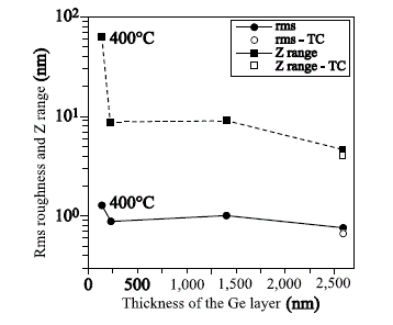
We used X-Ray Diffraction, in order to determine the macroscopic degree of strain relaxation (defined by ![]() = 5.65785 Å and aSi = 5.43105 Å, being respectively the in-plane lattice parameter of the epitaxial Ge layer and the bulk lattice parameters of Ge and Si). As an example, we will find in Figure 4.71, the omega-2theta scans around the (004) XRD order for the Ge layers imaged in Figure 4.69. The peak associated with the Ge layer shifts towards high incidence angles, and becomes narrower and more intense, when the thickness increases. We will note the strong asymmetry of the peak, when a thermal cycling is used. This asymmetry is due to an inter-diffusion between Si and Ge at the interface.
= 5.65785 Å and aSi = 5.43105 Å, being respectively the in-plane lattice parameter of the epitaxial Ge layer and the bulk lattice parameters of Ge and Si). As an example, we will find in Figure 4.71, the omega-2theta scans around the (004) XRD order for the Ge layers imaged in Figure 4.69. The peak associated with the Ge layer shifts towards high incidence angles, and becomes narrower and more intense, when the thickness increases. We will note the strong asymmetry of the peak, when a thermal cycling is used. This asymmetry is due to an inter-diffusion between Si and Ge at the interface.
The macroscopic degrees of strain relaxation are represented in Figure 4.72, according to the thickness of the deposited Ge layer. The 130 nm Ge “seed” layer deposited at 400°C is 95% relaxed. On the other hand, as soon as we go up to 750°C and we thicken the Ge layer, the latter is tensily-strained (R ~ 104–105%). This is at first paradoxical. We would indeed expect a compression state. This is however without the different coefficients of thermal expansion between Si and Ge [REE 96]. If we assume that a 2.5 µm Ge layer is completely relaxed at 750°C (i.e. R = 100%), and that the in-plane shrinking of the Ge lattice parameter occurs with the thermal expansion coefficient of the much thicker Si substrate underneath, we are at room temperature with Rtheor. = 105.4%, a value very close to those experimentally obtained [HAR 08e].
Figure 4.71. Omega-2 theta profiles around the (004) XRD order for various thicknesses of Ge layers on Si (001)
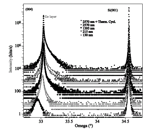
Figure 4.72. Macroscopic degree of strain relaxation functions of the thickness of deposited Ge
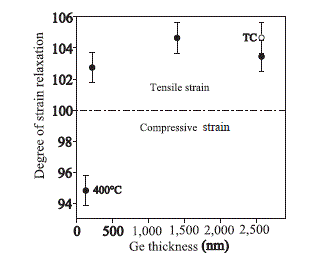
We imaged a thermally cycled, 2.8 µm thick Ge layer on Si(001) in Transmission Electron Microscopy (see Figure 4.73). There is a very important density of defects in the first 30 nm of Ge, as well as a significant number of misfit dislocations in the first micron. The top 1.8 µm of Ge is almost exempt of defects at the TEM scale, which likely means that the threading dislocations density is lower than 108 cm-2 [HAR 09b]. We thus carried wet chemical decorations (using Secco, Schimmel and chromium-free solutions) of the threading dislocations in these layers and we counted the etch pits using an optical microscope. Threading dislocations densities of about 107 and 5x107 cm-2 have been obtained in 2.5 µm thick Ge layers repectively with and without thermal cycling [HAR 09b]. We can also use in situ HCl defect decoration, in order to gain access to these densities.
Figure 4.73. Cross-sectional TEM image of the totality of a 2.8 µm thick, thermally cycled Ge layer on Si(001) (on the left) and zoom close to the Ge/Si interface (on the right)
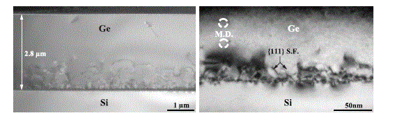
Figure 4.74. Amplitude mode AFM images of the surface of 2.5 µm thick Ge layers without (on the left) or with (on the right) thermal cycling after HCl decoration of the threading dislocations
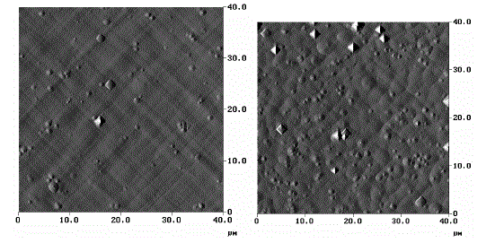
We will find in Figure 4.74 amplitude mode AFM images of the surface of 2.5 µm thick Ge layers thermally cycled or not, after the HCl etch of ~ 0.3 µm of Ge. The etch pit density is three times lower after thermal cycling: 7x106 cm-2 ![]() 2x107 cm-2. The fact that ~ 1 µm of Ge was consumed during wet chemical defect decorations probably explains why higher threading dislocations density values found: we are indeed closer to the dislocated area [HAR 09b].
2x107 cm-2. The fact that ~ 1 µm of Ge was consumed during wet chemical defect decorations probably explains why higher threading dislocations density values found: we are indeed closer to the dislocated area [HAR 09b].
Finally, we used secondary ions mass spectrometry, in order to have access to the Si and Ge depth profiles in these thick layers (see Figure 4.75). A significant penetration of the Si atoms (coming from the substrate) in the Ge layer is highlighted after an “aggressive” thermal cycling (in this case, 10 x {750°C, 10 min/900°C, 10 min}). This is harmful for the absorption properties of Ge in a photo-detector, but has a priori only little impact from the electric transport point of view.
Figure 4.75. SIMS profile of the concentration in Si and Ge atoms in thick Ge layers thermally cycled or not deposited on Si (001). The interface is symbolized by a dotted line
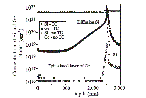
The first hundred nm (from the surface) of these thermally cycled thick Ge layers can be transferred thanks to the SmartCutTM process on oxidized Si substrates [AUG 09, CLA 06]. We thus obtain GeOI substrates of excellent crystalline quality, as shown in Figure 4.76. The density of threading dislocations in these GeOI substrates is indeed about the same, as the one of the Ge starting layers [ABB 07c].
Figure 4.76. Cross-sectional TEM images of a GeOI substrate fabricated with a thick layer of Ge deposited on Si(001)
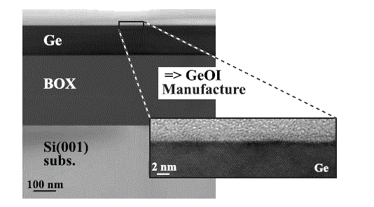
4.7.3. Optical and transport properties of thick Ge layers on Si (001) and of GeOI substrates
First of all, we will take a look at the optical properties of thick Ge layers on Si(001). In Figure 4.77, we will find the absorption coefficient of Ge layers of various thicknesses, functions of the wavelength. Despite the fact that these layers are dislocated, very high absorption coefficients are obtained at 1.3 μm (10,000 cm-1), as well as at 1.55 μm (4,500 cm-1). The slight tensile strain present in these Ge layers (see Figure 4.72) generates a decrease of about 30 meV of their direct energy bandgap (which determines the absorption threshold). We go indeed from 0.81 eV for bulk Ge to 0.78 eV for epitaxial Ge on Si, which is most interesting for photo-detection at 1.55 μm. We thus could obtain high-speed Metal-Semiconductor-Metal [VIV 07] and vertical p-i-n [VIV 09] Ge photo-detectors, at 1.31 as well as at 1.55 μm. To that end, we selectively grew several hundred of nm up to more than one micron thick Ge layers in Si cavities at the end of SOI waveguides, thanks to a low /high temperature growth strategy, without subsequent thermal cycling.
The latter is indeed harmful for thin Ge layers: the GeSi alloy, then formed, (from the Ge/Si interdiffusion) absorbs light in the near infra-red far less efficiently than pure Ge [HAR 10b]. In the case of p-i-n Ge photo-detectors, Ti/TiN/AlCu electrodes have then been deposited and etched, in order to contact the higher and lower in situ doped layers (see Figure 4.78). A cut-off frequency at -3dB, able to go up to 42 GHz at 1.53 μm, was then obtained (see Figure 4.79).
Figure 4.77. Absorption coefficient of bulk Ge and of various thickness Ge layers deposited on Si(001), functions of the wavelength
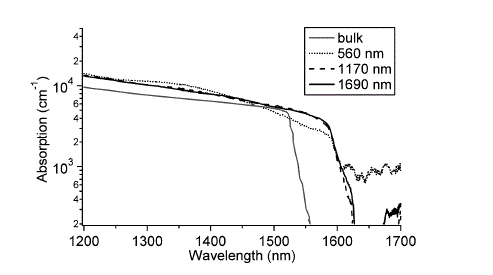
Figure 4.78. Top view optical microscopy image of a Ge photo-detector inserted at the end of a ridge optical waveguide
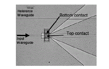
It is possible, when combining the tensile strain present in Ge layers deposited on Si(001) and n-type phosphorous ion implantation, to obtain an intense emission of light at a wavelength of about 1.6 µm, at room temperature [SUN 09]. The electrons given by the n-type impurities to the Ge crystalline lattice then occupy the L valleys of the conduction band, exalting the direct transitions between the Γ valley of the conduction band and the heavy and light holes sub-bands of the valence band. A room temperature laser has thus been obtained [LIU 10], letting us believe for the near future in the monolithic integration of IV-IV light emitters, optical waveguides, modulators [MAR 09] and photo-detectors on Si substrates.
Figure 4.79. Normalized optical functions of the frequency for a Ge pin diode integrated at the end of a ridge SOI optical waveguide for 0, -2.0V and -4.0 V applied voltages, this for a 1.53 µm wavelength. The length of the Ge photo-detector is 15 µm and the width of the ridge is 3 µm
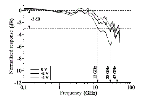
Figure 4.80. Cross-sectional TEM image of a pMOSFET transistor on GeOI
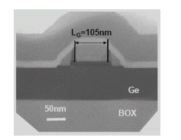
We will now briefly show the electric properties of pMOSFETs transistors fabricated on GeOI SmartCutTM substrates (see Figure 4.80) [POU 08, POU 09, ROY 08, VIN 10]. The integration scheme is as follows: after the definition of mesas on the GeOI substrate, a surface passivation of Ge by 1 to 2 nm of epitaxial Si is carried out [HAR 09b, HAR 10b, MIT 09]. This Si layer, partially chemically oxidized, is then covered with a HfO2/TiN/poly-Si gate stack.
The gates are then patterned using ultra-violet lithography, the extensions are implanted using BF2, the HfO2/SiN spacers are etched and the sources and drains are BF2 implanted. The thermal budgets of the post implantation activation anneals and those of the various deposition steps, have been lowered. Those pMOSFETs are indeed fabricated on GeOI substrates, and not SOI substrates (temperature of solid-liquid transition for Ge: 928°C ![]() 1,414°C for Si). From the device point of view, we have been confronted to the appearance of a parasitic channel at the interface between Ge and the buried oxide generating a very important off-state current and thus a degraded ION/Ioff trade-off. The use of a high backside voltage VBG = 60 V (for an intrinsic GeOI substrate), the insertion of a thin Si passivation layer between Ge and the buried oxide [ROM 09] or a counter-doping using phosphorus atoms, yielded good pMOSFET characteristics, however (i.e. a negative threshold voltage and a ION/Ioff trade-off higher than 104), as illustrated in Figure 4.81.
1,414°C for Si). From the device point of view, we have been confronted to the appearance of a parasitic channel at the interface between Ge and the buried oxide generating a very important off-state current and thus a degraded ION/Ioff trade-off. The use of a high backside voltage VBG = 60 V (for an intrinsic GeOI substrate), the insertion of a thin Si passivation layer between Ge and the buried oxide [ROM 09] or a counter-doping using phosphorus atoms, yielded good pMOSFET characteristics, however (i.e. a negative threshold voltage and a ION/Ioff trade-off higher than 104), as illustrated in Figure 4.81.
Figure 4.81. Low drain voltage ID - VG characteristics, with and without P counter-doping, for 0 and 60 V backside voltages
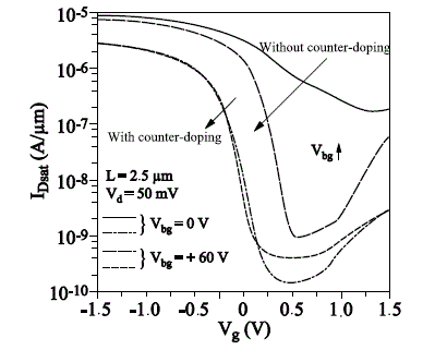
Holes mobilities in these pMOSFET GeOI transistors are twice higher with or without channel counter-doping, than those in FD-SOI transistors. With implanted pockets (control of short channel effects), they are 1.5 times higher (see Figure 4.82). The horizontal or vertical co-integration with SOI (or sSOI) on the nMOS side and GeOI on the pMOS side can consequently be used, in order to obtain high efficiency complementary MOS components [BAT 09b].
Figure 4.82. Holes mobility according to the gate length in pMOSFET GeOI transistors with and without counter-doping and in pMOSFETs FD-SOI transistors
In order to be exhaustive, it is possible, thanks to the Ge enrichment method, to obtain GeOI substrates without using the SmartCutTM method. In this approach, we start from thinned down SOI substrates, on which low Ge concentration SiGe layers are deposited. Thanks to high temperature dry oxidation steps, it is then possible to selectively oxidize the Si atoms and to push, thanks to a “snow-plough” effect, the Ge atoms towards the buried oxide. We thus obtain very high Ge concentrations, thin (~ 10 nm) SiGe layers, on which pure Ge layers of pure Ge are then deposited [NGU 07]. Thanks to various device integration improvements, a ION/IOFF trade-off exceeding 105 has recently been obtained in pMOSFETs transistors fabricated on this type of substrate [HUT 10b].
4.7.4. Structural and optical properties of Ge islands on Si (001)
In order to conclude section 4.7, we will take a look at the growth of Ge islands on Si (001) and at the optical properties obtained when those are encapsulated by Si [HAR 05c, DAM 04b]. When we deposit Ge on Si at relatively high temperatures (about 600°C-700°C in RP-CVD, lower in molecular beam epitaxy), we have, because of the compressive strain stored in the Ge layer, a growth mode called Stranski-Krastanov, i.e. an initially 2D growth mode, which becomes 3D (formation of islands) when it is energetically favorable that the surface undulates (elastic relaxation of the built-in strain).
These Ge islands have intensively been studied these last 20 years, with the objective of benefitting (post-encapsulation by Si) of quantum effects in IV-IV semiconductor heterostructures. Their sizes, shapes and surface density depend on the amount of Ge sent on the surface, on the temperature and on the growth pressure, etc., [HER 99, KAM 97, KUR 02a, KUR 02b, KER 04, LOO 01, MO 90]. Low growth temperatures are indeed recommended, in order to obtain high densities of pyramidal Ge islands with {105} facets. With higher growth temperatures, we will probably have islands nucleation in the shape of domes, with higher slopes.
In Figure 4.83, we will find 1 µm x 1 µm AFM images of the surface for various numbers of Ge monolayers sent at 600°C, 20 Torr on Si(001). The growth rate is about 1.5 nm min.-1 for a F(GeH4)/F(H2) = 4.17x10⁻⁵ mass-flow ratio. The surface is smooth for 3.9 atomic monolayer of Ge (i.e. 5.7 Å). On the other hand, for 5.1 atomic monolayers of Ge, there is an appearance of a substantial number of {105} pyramids. When the number of atomic monolayers goes from 5.1 to 15.3, these pyramids grow in size and gradually evolve into domes.
We extracted from such AFM images the surface density of the islands, as well as their average diameter and height functions of the number of atomic monolayers of Ge deposited at 600°C or 650°C on Si (001) (see Figure 4.84). The total density of islands (pyramids + domes) is much lower at 650°C than at 600°C: 9.4x109 cm-2![]() 2.4x1010 cm-2. We have an increase in the surface density of domes, at the expense of one of the pyramids, when the number of atomic monolayers of deposited Ge increases.
2.4x1010 cm-2. We have an increase in the surface density of domes, at the expense of one of the pyramids, when the number of atomic monolayers of deposited Ge increases.
In addition, let us notice that the diameters of the pyramids and domes are relatively independent from the number of Ge monolayers deposited, but depend however on the growth temperature: the higher it is, the larger the diameter will be (between 60 and 90 nm).
Figure 4.83. Evolution of the surface morphology functions of the number of atomic monolayers of Ge deposited at 600°C on Si (001)
The height of the pyramids is, as expected, constant at ~ 5 nm, given the relative stability of their diameter ({105} facets). On the other hand, the height of the domes definitely increases with the growth temperature and the number of Ge atomic monolayers deposited. It reaches values higher than 20 nm for 15 atomic monolayers.
Figure 4.84. Evolution ( from left to right, from top to bottom) of the density, of the diameter and of height of the Ge pyramids or domes, functions of the number of atomic Ge monolayers deposited at 600°C, as well as 650°C on Si (001). The diameters of the islands are most likely over-estimated because of the convolution between the shape of the AFM tip and the actual surface
A single plane of Ge islands deposited at 600°C on Si (001) has been encapsulated by 150 nm of Si and has been studied at T = 10 K in photoluminescence. We will find the spectra obtained in Figure 4.85. The impact of the number of Ge atomic monolayers on the energy position of no-phonon (NP) lines and of their replica, assisted by an optical transverse phonon (TO) is illustrated in Figure 4.86. These lines shift towards low energies, i.e. towards large wavelengths, when the number of Ge atomic monolayers increases. It is thus possible to tune the properties of luminescence of these Ge quantum islands, functions of the applications aimed for (emission at 1.3 or 1.55 μm).
Figure 4.85. Photoluminescence spectra associated with a single plane of Ge islands capped with Si, according to the number of Ge atomic monolayers deposited
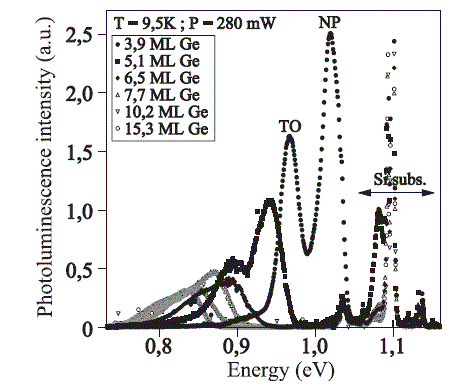
Multiple planes of Ge islands (with tens of nm thick Si spacers) can be stacked one upon the other in order to exalt the luminescence output per surface unit. Depending on the thicknesses of the Si spacer layers, there will be either a vertical alignment of the islands one above the other, or a “A-B-A-B” stacking (presence of stress fields in these stacks) [DAM 04b, KER 04]. Rather interesting photo- or electro-luminescence properties at 0.8 eV, i.e. 1.55 μm, have then been obtained.
Figure 4.86. Energy positions of the NP and TO lines functions of the number of Ge atomic monolayers deposited
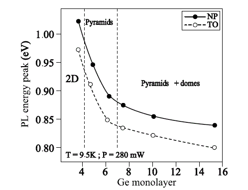
4.8. Devices based on sacrificial layers of SiGe
4.8.1. Introduction
To be able to etch several nanometers thick mono-crystalline layers selectively compared to others is mandatory in order to obtain localized SOI or silicon-on-nothing devices [MON 07, MON 10], multi-wires [DUP 08a, DUP 08b, TAC 09] or multi-channels [BER 08, BER 09a, BER 09b] transistors, etc. In the following figures, we will show a schematic description of the technological steps leading to some of these structures.
All these devices rely on the fact that, in pseudomorphic SiGe/Si stacking, it is possible to laterally etch SiGe layers with a Ge concentration higher or equal to 20%, selectively compared to Si. This obviously presupposes having lateral access to said SiGe layers, thanks to anisotropic etching steps (definition of mesas) or to more complex sequences of technological steps [DUT 07]. Several techniques are available for these selective etchings. A plasma etching at low pressure and room temperature with CF4 as a precursor gas is normally used [BAR 08, BOR 06]. We can also call upon wet chemical solutions, such as HF:HNO3:CH3COOH [HOL 10, SAL 08]. In the first case, we will have etching selectivity between 60 and 100 (depending on the Ge concentration of the layer). In the second case, the selectivity will be about 200 [SAL 08]. The etching will be perfectly isotropic in both cases.
The last few years, we explored a third option: thermal HCl etching directly in the epitaxy chamber [BOG 06c, DES 08a, DES 08b]. This technique will be presented in section 4.8.2.
4.8.2. Selective HCl etching of SiGe selectively compared to Si
In 2004, we profited from the fact that gaseous hydrochloric acid cannot etch SiO2 or Si3N4, in order to etch on patterned substrates the Si windows surrounded by oxide (shallow trench isolation or STI). These cavities were filled afterwards with several hundred nm of Si0.8Ge0.2, the idea being to locally have thin SiGe virtual substrates, on which tensily-strained Si layers can then be deposited [BOG 05e, DEL 04]. That is why we studied the etching kinetics of Si, of Si0.65Ge0.35, of Si0.5Ge0.5 and of Ge. We found ourselves in the presence of (i) a high temperature regime, where the etch rate dependence on the Ge concentration is low, and (ii) a low-temperature regime, where the etch rate dramatically increases with the Ge concentration. From this came the idea to use HCl, in order to laterally etch SiGe selectively compared to Si, idea whose feasibility we proved in 2006 [BOG 06c]. Relatively high etching temperatures (typically 700°C) were then necessary (because of the low total pressure (20 Torr) and the low partial pressure of HCl (0.208 Torr)), in order to have reasonable etching rates. We thus increased the total pressure, as well as the HCl partial pressure in considerable proportions: 300 Torr and 180 Torr, respectively.
We thus could increase by a factor of 10 (at given temperature) the etch rate of Si and have substantial SiGe etch rates at rather low temperatures (see Figure 4.87) [DES 08a]. In Figure 4.88, we can see the theoretical selectivities expected (by dividing at a given temperature, the vertical etch rate rate of SiGe by the (extrapolated) vertical etch rate of Si). Those are about 30 for Si0.8Ge0.2, 200 for Si0.7Ge0.3 and 5,000 for Si0.6Ge0.4!
What about the lateral selectivity of the etching of SiGe compared to Si? In order to evaluate it, we deposited SiGe 20 nm/Si stacks with various Ge concentrations, that we capped with deposited oxide. Optical lithography and anisotropic etching (all the way to the Si substrate underneath) was then used in order to define to have access laterally to the Si and SiGe layers (various size mesas with <110> sidewalls). In Figure 4.89, we will find a cross-sectional scanning electron microscopy image of such a stack, after an HCl etching at 650°C for twenty minutes.
Figure 4.87. Etch rate of Si (for partial pressures of HCl of 0.208 and 180 Torr) and of SiGe (partial pressure of HCl equal to 180 Torr), functions of the opposite of the absolute etching temperature
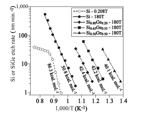
Figure 4.88. Theoretical selectivities expected functions of the etching temperature, for Ge concentrations of 20%, 30% and 40%
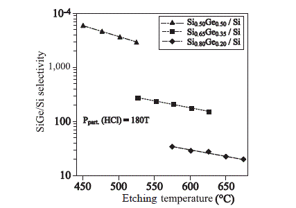
We can notice that, as expected, the depth of the channels dramatically increases with the Ge concentration: it goes from 20 nm for Si0.8Ge0.2 to 270 nm for Si0.7Ge0.3 to 740 nm for Si0.6Ge0.4. Selectivities of 100 for Si0.7Ge0.3 and of 130 for Si0.6Ge0.4, are associated with this high HCl partial pressure lateral selective etching [SAL 08].
However, we did not succeed in selectively etching Si0.8Ge0.2 layers compared to Si, even by playing with the etching parameters. This is one of the restrictions of HCl etching, compared to the dry plasma and wet etching techniques. We used cross-sectional transmission electron microscopy, in order to visualize more precisely these channels (see Figure 4.90). Floors and ceilings of tunnels are smooth. <111> facets are otherwise present at the end of the tunnels. Moreover, we can note, in Figures 4.89 and 4.90, that the SiGe layers, located at the bottom of stackings, are slightly more etched than those at the top. With given process parameters, <110> lateral SiGe etch rates are, for 20 nm thick SiGe layers, approximately ten times lower than the vertical etching rates (along [001]) of Figure 4.87.
Figure 4.89. Cross-sectional SEM images of SiGe 20 nm/Si stacks after HCl etching at 650°C for twenty minutes (P(HCl) = 180 Torr)
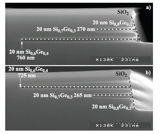
Figure 4.90. Cross-sectional TEM images of a Si0.6Ge0.4 20 nm/Si multilayer after HCl etching at 610°C for twenty minutes (P (HCl) = 180 Torr)
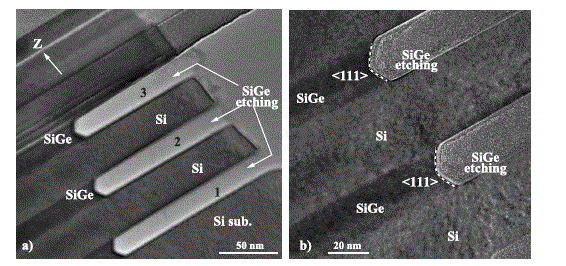
The isotropy of the HCl etching method is thus questionable. A top view SEM image of patterned SiGe/Si stacks after HCl etching can be found in Figure 4.91 (mesa edges are along the <110> directions). The regions where SiGe has been removed are clearly seen (electron transparency differences with regions where SiGe is still present). We clearly have at the corners of these <110> elongated lines <113> facets, related to a etch rate which is much higher in the [100] and [010] directions than in the <110> directions. The HCl etching method is thus definitely anisotropic, contrary to the other two.
Figure 4.91. Top-view SEM images of several tens of μm long mesa lines etched anisotropically in a (20 nm Si0.6Ge0.4/40 nm Si) x3 superlattices, which was laterally etched later on at 600°C for twenty minutes (P (HCl) = 180 Torr)
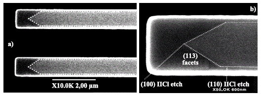
We can add that with the HCl method, lateral etch rates definitely depend on the thickness of the SiGe layer. An increase by 18 of the etch rate has indeed been noticed, by going from 5 to 20 nm thick Si0.6Ge0.4 layers [DES 08b].
Because of these restrictions, we did not use HCl selective etching of SiGe compared to Si on the 200 mm localized-SOI and SON electrical lots processed in CEA-LETI. Our set of lithography masks impose the presence of anchors on both sides of the active central zone, which will be hollowed out and then filled by a dielectric, so that the whole pattern (in shape of a bone) does not collapse. However, it seems that these anchors are preferentially consumed compared to the active zones during anisotropic HCl etching [DES 08a]. On the other hand, 300 mm L-SOI and SON technologies do not require anchors: the small area Si slabs on top are kept rigid by the gate during selective etching. This justifies the adoption of HCl etching at STMicroelectronics Crolles [MON 07, MON 10].
4.8.3. Localized SOI devices and SON
We will find in Figure 4.92, a schematic description of the main technological steps used for the fabrication of localized SOI devices [MON 07]. We start from patterned Si (001) substrates with STI isolation. After a {“HF-last” wet cleaning / in situ H2 bake at 850°C} surface preparation, the active zones of Si are partially recessed (consumption of approximately 20–30 nm) using HCl [DES 07, HAR 06b]. After that, a {sacrificial layer of Si0.7Ge0.3/Si channel} stack is selectively deposited compared to SiO2 using chlorinated chemistry, by taking into account obviously the loading effects inherent in any SiGe epitaxy on a patterned substrate (see section 4.2). The desired thicknesses of Si0.7Ge0.3 and of Si are respectively about 15–20 nm and 10–20 nm.
Having hollowed out the active zones prior to epitaxy, we can thus avoid the formation of facets at the {active zone — STI} boundaries [COL 03, DUT 07]. Indeed, the flanks of the STI are then entering, instead of being open (see Figure 4.93).
A (HfO2/TiN/poly-Si) gate stack is then deposited and etched and nitride spacers are fabricated. Si raised sources and drains (typically 20 nm thick) are then selectively deposited (thanks to the method described in section 4.4) and ions implanted. STI zones are then lowered thanks to a de-oxidation in a diluted HF bath, in order to have lateral access to the SiGe sacrificial layers. Those are selectively etched compared to Si, thanks to the CF4 plasma etching technique (in 200 mm technology) or with a HCl etching (in 300 mm). We have then at this stage a suspended Si channel under the gate.
Figure 4.92. Schematic description of the main technological steps used to fabricate L-SOI devices
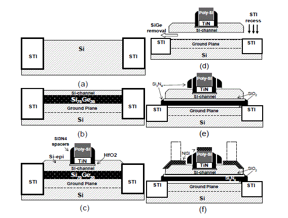
The space previously occupied by SiGe is then filled in a conformal fashion by a SiO2/Si3N4 stacking. The sources and drains are then Ni silicided, prior to the so-called “back-end” process steps, where the metal interconnections are fabricated between the individual transistors. The perfectly single-crystal Si channel under the gate (thickness greater than or equal to 5 nm), is above a thin buried dielectric. That is why it is called localized SOI (we indeed started from massive Si substrates and not from SOI substrates).
In the literature, we can find a variant of the localized SOI method, called Bulk+ [MON 10]. The differences compared to the localized SOI method described in Figure 4.92, are as follows: after definition of the gate stack (see Figure 4.92c), the source and drains zones are anisotropically etched until the Si substrate is reached. We then have lateral access to the SiGe sacrificial layer under the gate, without needing to lower the STI zones. This layer is selectively etched compared to Si and the space left vacant is filled (as for the localized SOI) by a SiO2/Si3N4 stacking.
Figure 4.93. Cross-sectional SEM or TEM images of the SiGe/Si stack (b) and of a L-SOI transistor (f)
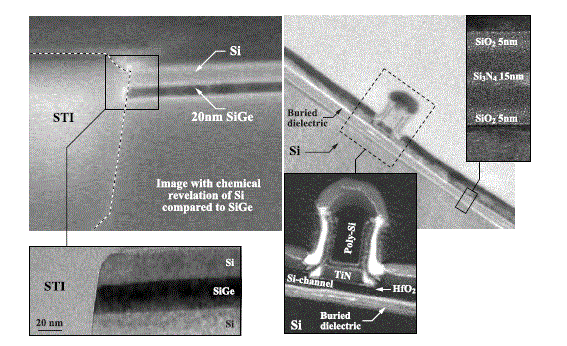
We then proceed to a selective epitaxy of about 30–40 nm of Si in the sources and drains areas, in order to connect the Si channel under the gate. We will find in Figure 4.94, a cross-sectional TEM image of a Bulk + transistor, for the 32 nm technological node obtained at ST Microelectronics Crolles [BID 08, BID 09a].
Figure 4.94. Cross-sectional TEM image of a Bulk + 32 nm transistor with HfO2/TiN/poly-Si gate stack
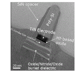
Electric performances relatively similar to those of FD-SOI transistors, have been obtained with Bulk+ and localized SOI devices [MON 10]. We thus have a low cost co-integration strategy of “SOI-like” and “bulk” devices on the same bulk Si wafer (instead of starting from a much more expensive SOI substrate). Nothing indeed prevents us from selectively depositing SiGe/Si stacks in part of the Si windows of a patterned substrate, (which will be the core of upcoming Bulk+ or localized SOI transistors), the remaining windows being masked (sites of upcoming “bulk” transistors) [MON 10].
A certain number of recent developments were undertaken in order to improve the electric performances of localized SOI pMOS transistors. We notably carried out, after the etching of the SiGe sacrificial layer, a selective epitaxy of approximately 30 nm of Si0.65Ge0.35. The Ge atoms of this layer were pushed back towards the SiO2/Si3N4 stacking, thanks to the Ge enrichment technique (i.e. a high temperature oxidation of the SiGe layer generating: (i) the formation of SiO2 and (ii) the movement by a “snow-plough” effect of the Ge atoms towards the buried dielectric [NGU 07]). We thus locally obtained a dozen nm thick, very high Ge concentration GeSi layer, on which a gate was deposited and then etched. We then speak of germanium-on-nothing or GeON devices [BAT 07, BAT 08].
A second integration option has been developed, in order to have pMOS GeON transistors. A {2.3 nm pure Ge/1.3 nm Si} stack has therefore been selectively deposited at low-temperature on the Si surface layer (after etching the SiGe sacrificial layer underneath and filling the cavity thus formed by dielectrics). With: (i) the Ge/Si interdiffusion occurring during the epitaxy step itself and (ii) the thermal budget (even carefully minimized) of the subsequent technological steps, we obtain a GeSi channel (and not pure Ge) under the gate of our pMOS transistors. A 60% gain in the mobility of the holes in this channel (compared with Si) was nevertheless highlighted, stressing the interest of the approach [BAT 08].
Another way of gaining hole mobility would be to go from standard (001) to (011) crystalline planes [BID 09b, OKA 07, SHA 05, SHE 05]. These gains would be even higher by going from Si (011) to SiGe (011) [JOS 07, PAN 06]. The final objective being to fabricate high mobility localized SOI (011) pMOSFETs, we thus studied on blanket substrates the impact of the crystalline orientation on: (i) the efficiency of the H2 bake that follows “HF-last” wet cleanings, (ii) the Si etch kinetics with HCl and (iii) the growth kinetics of Si and SiGe (the precursor gases being SiH2Cl2 and GeH4) [DES 08c, DES 10, HAR 06c]. Briefly, a H2 bake temperature ≥ 800°C is mandatory on Si(001) and Si(011) surfaces, in order to be free from any C or O residual contamination. Si HCl etch rates are (between 750°C and 950°C) four times higher on (011) than on (001). The associated activation energies are however close to one another (57 kcal mol.-1 on (100) ![]() 59 kcal mol.-1 on (100)). The SiGe (011) growth rate at 600°C and 650°C increases parabolically then saturates when the GeH4 flux increases. It however increases in an almost linear way on (001), reaching at 650°C, values three times higher than those on (011) for high GeH4 flows. The parabolic relation provided in section 4.2 satisfactorily describes on (001) the dependence of the Ge concentration (between 10% and 37%) with the F(GeH4)/F(SiH2Cl2) mass-flow ratio. This relation is on the other hand linear on (011). The ratio between the Si(011) and the Si(001) growth rates, ~ 0.74, is close to the ratio of dangling bonds densities on the surface, i.e. 0.71. Activation energies of 63 and 65 kcal.mol.-1 are associated with the increase of the Si growth rate with the temperature on (001) and (011).
59 kcal mol.-1 on (100)). The SiGe (011) growth rate at 600°C and 650°C increases parabolically then saturates when the GeH4 flux increases. It however increases in an almost linear way on (001), reaching at 650°C, values three times higher than those on (011) for high GeH4 flows. The parabolic relation provided in section 4.2 satisfactorily describes on (001) the dependence of the Ge concentration (between 10% and 37%) with the F(GeH4)/F(SiH2Cl2) mass-flow ratio. This relation is on the other hand linear on (011). The ratio between the Si(011) and the Si(001) growth rates, ~ 0.74, is close to the ratio of dangling bonds densities on the surface, i.e. 0.71. Activation energies of 63 and 65 kcal.mol.-1 are associated with the increase of the Si growth rate with the temperature on (001) and (011).
With such data, we have been able to manufacture on patterned Si(011) substrates with STI isolation, high electric performances L-SOI transistors. Hole mobility gains as high as 250% were demonstrated [DES 10].
4.8.4. Devices based on multi-wires and on multi-channels
In order to gain in terms of current density per surface area, it could be interesting to stack conduction channels onto one another. A gate-all-around configuration them would lead to a better control of short channel effects for very small gate lengths. This is possible with architectures, known as “multi-channels” and “multi-wires”.
We will find in Figure 4.95, a schematic description of the main technological steps used for the fabrication of multi-channels transistors. We start by depositing a Si/SiGe multi-layer on a blanket SOI substrate (step 1). Then, the active zones are defined (“mesa” isolation between those, i.e. we etch the Si/SiGe stack until the buried oxide). The gates are then defined thanks to the use of a hard mask, of a hybrid (UV/e-beam) lithography and of an anisotropic etching, stopping on the Si layer of the starting SOI substrate (step 2). A Si selective epitaxy in the source and drains zones on both sides of the gate is then carried out, in order to connect the piled up Si channels (step 3), followed by multiple ion implantation steps (to dope the S/Ds).
Then, the SiGe sacrificial layers are selectively etched, compared to those of Si, thanks to isotropic plasma etching (step 4). The cavities thus formed are filled in a conformal fashion by a HfO2 / TiN / poly-Si gate stack. After the deposition of spacers, the source and drain zones are silicided (step 6). We thus obtain a multichannels transistor, as illustrated by the cross-sectional TEM image in Figure 4.95.
We will find in Figure 4.96 a schematic description of the main technological steps leading to, this time, multi-wires transistors. We find the epitaxy of a Si/SiGe multi-layer on SOI (step 1), the anisotropic etching of an array of “fins” between the sources and drains blocks (step 2), the selective etching of the SiGe sacrificial layers (step 3), the conformal deposition in the cavities thus formed, as well as between the “fins” of the same type of gate stack as for multi-channels (step 4), the anisotropic etching that follows leading to the obtainment of either etched gates (step 5a), or “plugged” gates (step 5b), followed by multiple ion implantation steps and silicidation of sources and drains (step 6) and then by metal interconnections (step 7).
Figure 4.95. Description of the various technological steps used in order to fabricate multichannels transistors and cross-sectional TEM image of a transistor with 5 channels
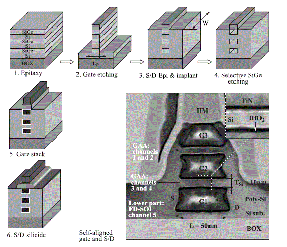
We notice that, for the two integration schemes, it is essential to obtain on SOI substrates Si/SiGe stacks which are in fact regular super-lattices. The individual thicknesses of the Si and SiGe layers will indeed dictate the dimensions according to z of the Si wires and of the spaces between those. And yet, the presence on SOI substrates of a buried oxide will significantly influence the growth kinetics of Si and SiGe, according to the deposited thickness, as we will see below [HAR 09a].
Figure 4.96. Description of the various technological steps used for multi-wire transistors fabrication, top-view SEM images of multi-wires transistors with etched gate and “plugged” gate and cross-sectional TEM image of a transistor with 3 wires (perpendicular to the transistor)
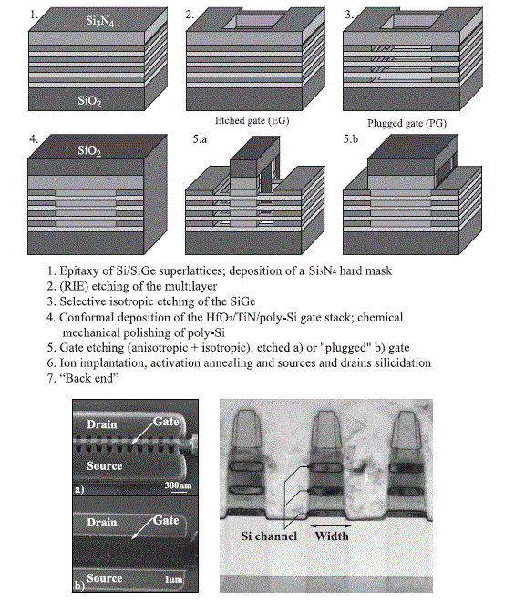
We will find in Figure 4.97 cross-sectional TEM images of two 19 periods Si/Si0.8Ge0.2 superlattices deposited at 650°C, 20 Torr on a bulk Si(001) substrate and on a {20 nm Si/145 nm buried oxide} SOI substrate, this using the same epitaxy recipe. Individual thicknesses of SiGe and Si layers are, as expected, constant on a bulk Si(001) substrate. Those on a SOI substrate are almost equal to those on a massive substrate for the first period. They however drop dramatically for the following periods, and then increase again when the deposited thickness increases.
Figure 4.97. Cross-sectional TEM images of two 19 periods Si/Si0.8Ge0.2 superlattices deposited at 650°C, 20 Torr on a {20 nm Si/145 nm buried oxide} SOI substrate (left) and a bulk Si(001) substrate (right). Same epitaxy recipe used in both cases
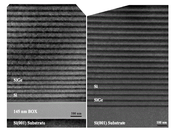
We will find in Figure 4.98, the growth rates associated with the Si and SiGe layers, and in Figure 4.99 the Ge concentration according to the thickness deposited on these two types of substrates (values obtained from SIMS profiles of the concentration in Ge atoms in the stackings above).
We find there the important drop, then the increase (followed by a small decrease) on the SOI substrate, of the growth rates of Si and SiGe. This evolution occurs at the same time as a small increase, followed by a decrease, and then again by a small increase in the Ge concentration. This is due to the surface temperature fluctuations, because of the presence of a buried oxide.
Figure 4.98. Si and SiGe growth rates according to the thickness deposited on a bulk Si substrate and on a SOI substrate
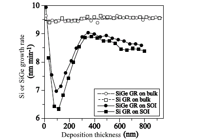
Figure 4.99. Ge concentration according to the thickness deposited on a bulk Si substrate and on a SOI substrate
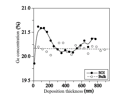
The surface temperature, about 650°C for the starting SOI substrate (i.e. 20 nm of Si on top of 145 nm of BOX), drops to approximately 638°C for 100 nm deposited, goes back up to approximately 648°C for 350 nm deposited, and then slowly decreases to approximately 646°C for 800 nm deposited. Thanks to calibration curves such as those in Figure 4.98, we were able in the past to grow well controlled SiGe/Si stacks on SOI substrates and thus obtain regular multi-channels or multi-wires structures [HAR 05b, HAR 09a]. We will note that the thickness of the buried oxide also has an impact on the growth kinetics that we must consider if we change the type of SOI substrate [HAR 04a].
Once the Si nanowires are released, it is possible to alter their shape, using in situ H2 annealing in the epitaxy reactor [DOR 07]. We can indeed go from Si wires of rectangular section (after selective etching of SiGe versus Si) to wires of circular section, while preserving an excellent crystalline quality, as shown in Figure 4.100. It is however necessary not to use too important thermal budgets, or else the nanowires’ junctions with the sources and drains blocks will get thinner and then break.
Once their section is rounded off, it is then possible to drastically reduce their diameter, using {thermal oxidation (peripheral Si converted into SiO2) / wet chemical de-oxidation} cycles [HUB 08]. We thus obtained arrays of Si nanowires with a diameter as low as 8 nm (as illustrated in Figure 4.101), or even below [ERN 09].
From the integration point of view, we also can take advantage of the possibility that we have to selectively etch (with a dry plasma process) Si compared to SiGe [CAU 06]. We thus obtain an array of SiGe nanowires (and not of Si). Those wires, once selectively encapsulated at 650°C by a few nm of Si [HAR 09b], have been integrated in pMOS transistors, with a gain of 50% regarding the holes mobility [TAC 09]. These SiGe wires could also be used as starting structures for the formation of almost pure Ge nanowires of lower dimensions, thanks to the Ge enrichment technique previously mentioned [NGU 07, SAR 09].
We also have to use, during the manufacture of multi-channels transistors, a relatively complex process in order to selectively thicken the source and drains zones (selective epitaxy of about a hundred nm or even more of intrinsic or in situ doped Si: step 3 of the Figure 4.95). The standard epitaxy recipe which is used to selectively grow 20 nm thick Si raised sources and drains on both sides of FD-SOI transistors [JAH 05] will not yield (with a growth duration change, of course) the selectivity desired for this type of thickness and architecture. We thus implemented a cyclic {selective deposition (SiH2Cl2+HCl) / etching (HCl)} process in order to gradually thicken at 750°C or 800°C, 20 Torr, the source and drains regions while suppressing the poly-Si nuclei being formed on the Si3N4 internal spacers and hard mask of the multi-channels transistors [HAR 10c]. As an example, we will find in Figure 4.102 examples of cyclic deposition/etch processes optimized or not (~ 10 nm of intrinsic or in situ doped Si deposited per cycle).
Figure 4.100. Cross-sectional TEM images of arrays of Si nanowires just after selective etching (a), (b), (c), (d) and after H2 annealing at 800°C for two minutes (e), (f), (g), (h)
It should be noted that the combination of an in situ doping of these Si raised sources and drains with subsequent ion implantation steps leads to a significant gain in terms of electric performances for such transistors, compared to intrinsic Si raised sources and drains implanted later on [TAC 10].
Figure 4.101. Cross-sectional TEM images of an array of Si nanowires of 8 nm diameter with a conformal encapsulation with a HfO2 / TiN / poly-Si gate stack
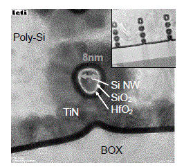
Figure 4.102. Cross-sectional TEM images of multi-channel transistors with Si3N4 internal spacers after the selective deposition of ~ 140 nm of Si:P or Si:B thanks to cyclic deposition/etching processes optimized (on the right) or not (on the left)
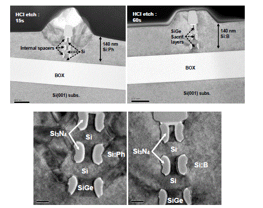
As a conclusion of this section 4.8, we will briefly show the electric characteristics associated with these multi-channel and multi-wire transistors. We will find in Figure 4.103 the drain currents associated with multi-channels nMOS and pMOS transistors with 50 nm effective gate length (see Figure 4.95) functions of the gate voltage. Exceptional on-state current / off-state current trade-offs (nMOS: ION = 2.27 µA /µm ![]() IOFF = 16.4 pA /µm, pMOS: ION = 1.32 mA /µ
IOFF = 16.4 pA /µm, pMOS: ION = 1.32 mA /µ ![]() Ioff = 16.75 pA /µm) are obtained thanks to this architecture and the HfO2/TiN/poly-Si gate stack [BER 08].
Ioff = 16.75 pA /µm) are obtained thanks to this architecture and the HfO2/TiN/poly-Si gate stack [BER 08].
We have compared in Figure 4.104, the drain currents associated with these five channels nMOS and pMOS transistors and with standard FD-SOI transistors with 50 nm effective gate length according to the difference between the gate voltage and the threshold voltage. A gain of a factor 4 – 5.5 (as geometrically expected) is obtained while moving over from single channel (i.e. FD-SOI) transistors to transistors with five channels piled up one above the other (MC-FET).
Figure 4.103. Drain current ID according to the gate voltage VG (drain voltages VD =± 0.05 V or ± 1.2V), this for five channels MC-FET transistors with 50 nm gate length
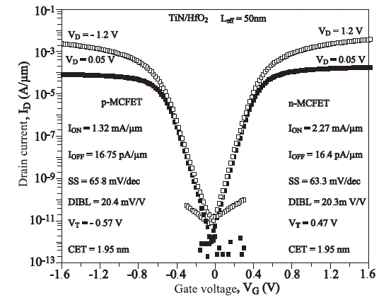
Figure 4.104. Drain current ID functions of the gate voltage VG - VT, (drain voltage VD =± 1.2V), for 50 nm gate length transistors with either one (FD-SOI) or five channels (MC-FET)
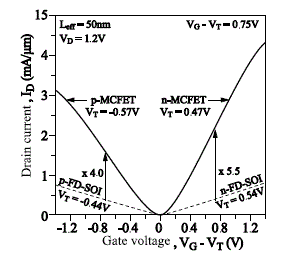
We will better realize the obtained electric performances by comparing in Figure 4.105, the ION/IOFF trade-offs of our multi-channels nMOS and pMOS transistors with those associated with other transistors from the literature (with simple planar gates, of the “FinFET” type or even with multi-channels, but with another gate stack (SiO2/poly-Si)).
Figure 4.105. Comparison of the ION /IOFF trade-offs of our multi-channels nMOS (on the left) and pMOS (on the right) transistors with those of other nMOS and pMOS transistors, aiming for Low Stand-by Power applications. Each point corresponds to a recent article of the literature. The currents are standardized by the gate width seen from the top
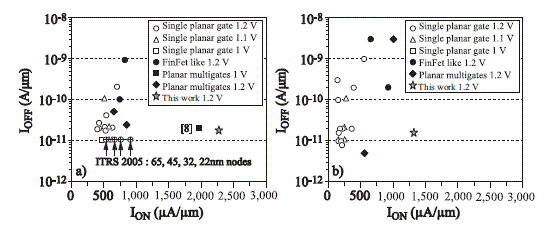
Extremely high on-state currents have recently been obtained for transistors based, this time, on ~ 15 nm diameter Si stacked nanowires (see Figure 4.106), at the detriment however of off-state currents which are more important than in multichannel transistors: (although the gate stack is the same): nMOS: ION = 6.5 mA /µm ![]() IOFF = 27 nA/µm, pMOS: ION = 3.3 mA /µm
IOFF = 27 nA/µm, pMOS: ION = 3.3 mA /µm ![]() IOFF = 0.5 nA/µm [DUP 08b]. These ION values, the highest published at this date, fully show the potentialities of this 3D architecture.
IOFF = 0.5 nA/µm [DUP 08b]. These ION values, the highest published at this date, fully show the potentialities of this 3D architecture.
Figure 4.106. Drain current ID according to the gate voltage VG (drain voltages VD =± 0.05 V or ±1.2V), for transistors with three stacked Si nanowires. The current is standardized compared to the diameter of the wires, approximately 15 nm (see the cross-sectional TEM image perpendicular to those Si NWs)
4.9. Conclusions and prospects
4.9.1. General conclusion
We briefly presented in section 4.1, the Reduced Pressure — Chemical Vapor Deposition tool used, as well as some epitaxy concepts essential to the understanding of the following of the chapter.
We described in sections 4.2 and 4.3, the specificities of the low-temperature epitaxy of thin SiGe (C) layers for the engineering of the channel of MOS transistors. The difficulties inherent in the selective epitaxy of SiGe in the Si windows of patterned substrates were highlighted (loading effects and surface roughness). We have also shown the strategy to adopt, in order to obtain SiGeC or Si1-yCy layers with record concentrations in substitutional C atoms (3.2% and 2.1%): a dichlorosilane (for SiGeC) or silane (for Si1-yCy) chemistry, a lowest possible growth temperature and a highest possible growth rate. Thanks to these studies, bulk, short gate length pMOS transistors with SiGe channels have been fabricated with hole mobilities twice as important and a lower threshold voltage (in absolute value) than in bulk Si. Low C concentration Si/SiGeC multi-layers inserted under the gate of bulk transistors lead to the reduction of: (i) the exo-diffusion of the atoms of B of the anti punch-through layer (pMOS) and (ii) the implantation depth of the As atoms in the sources and drains (nMOS), therefore to gain in terms of short channel effects. The situation is more contrasted for nMOS transistors with Si1-yCy channels: the electrons mobility is indeed lower or equal to that of bulk Si, but lower threshold voltages have been obtained from the alignment of the conduction band (because of the tensile strain).
Sections 4.4 and 4.5 were devoted to recessed or raised Si or SiGe:B sources and drains selectively grown on both sides of the gate of FD-SOI or SON transistors. Lowering on ultra-thin SOI substrates the in situ H2 bake temperature (650°C), as well as the epitaxy temperature (750°C, SiH2Cl2 + HCl) is mandatory, in order to avoid any withdrawal at the edge of active areas or islanding for initially less than 10 nm thick Si films. The impact of in situ B doping on (i) the resulting SiGe:B layers’ structural and electrical properties and (ii) the SiGe growth kinetics with a chlorinated chemistry has been described. Two demonstrations of Selective Epitaxial Growth of SiGe:B raised (FD-SOI) or recessed (SON) sources and drains have otherwise been presented.
In section 4.6, we took a look at the structural properties of SiGe virtual substrates and of the tensily-strained Si layers, which we can deposit on top. Thanks to the adoption of high growth temperatures (850–900°C), threading dislocations densities at the state of the art, i.e. 105 cm-2, and almost fully relaxed constant composition SiGe top layers have been obtained. By changing the Ge concentration between 20% and 50%, we could change the tensile strain in the sSi layers between 1.3 and 3.15 GPa, while preserving a good crystalline quality and smooth layers (thanks to the use of chemical-mechanical polishing steps of our virtual substrates, which are strongly undulated (i.e. “cross-hatched”) right after epitaxy). These sSi layers, transferred on oxidized Si substrates, form the core of sSOI substrates. Gains of a factor of 2 of the electrons mobility (compared to bulk Si) have been obtained in nMOS transistors fabricated on tensily-strained Si layers. Gains of a factor 2 of holes mobility have been similarly been obtained, by inserting between these sSOI substrates and the gate stack of the pMOS transistor a thin SiGe layer in compression, encapsulated by a few nm of Si. Thanks to an epitaxy on Si0.5Ge0.5 virtual substrates of a {compressively-strained Ge channel / tensily-strained Si cap} bi-layer, we have otherwise demonstrated a gain of a factor of 9 of the holes mobility and of a factor of 6 of the on-state current (compared to bulk Si), and have thus balanced the performances of nMOS and pMOS transistors.
Section 4.7 shows the interest to deposit thin or thick Ge layers directly onto Si substrates. A low-temperature/high temperature growth strategy for Ge, followed by a thermal cycling yield thick, smooth Ge layers, that are slightly tensily-strained and with a relatively low threading dislocations density, i.e. 107 cm-2. Thanks to the SmartCutTM process, good structural and electrical quality GeOI substrates were thus obtained, with a hole mobility gain of a factor of 2 in pMOSFET transistors fabricated on top. Superior performance photo-detectors operating in the near infrared (1.3 – 1.55 μm) have moreover been developed, thanks to the Selective Epitaxial Growth in Si windows at the end of optical waveguides (on SOI substrates) of several hundreds of nm thick pure Ge layers. Measurements in photoluminescence of single or multiple planes of Ge islands encapsulated Si have finally illustrated the possibility to modulate the emission wavelength of these islands, by modifying the number of Ge atomic monolayers, the thickness of the Si spacers between Ge islands planes, etc.
Lastly, section 4.8 was devoted to devices based on sacrificial SiGe layers. Multiple techniques are indeed available in order to laterally etch SiGe layers selectively compared to Si (plasma, wet and thermal (HCl) etching). Those are used in order to obtain localized-SOI or Silicon-On-Nothing devices. The space previously occupied by the SiGe layer is then filled in a conformal fashion by buried dielectric or the gate stacks. We thus obtain on bulk Si substrates, L-SOI and SON transistors functioning in the fully-depleted mode, without suffering from the costs associated with the use of SOI substrates. Thanks notably to the deposition on SOI substrates of SiGe/Si superlattices, it is possible thanks to a relatively complex integration scheme to obtain multi-channel or multi-wire transistors. Superior On-state currents as well as exceptional ION/IOFF trade-offs per surface unit were thus obtained, because of the stacking according to z of the charge carrier channels in these type of structures.
4.9.2. Prospects
In the previous chapters, we have been able to realize the degree of smoothness and of electronic quality of the Si/SiGe heterostructures that can be obtained thanks to reduced pressure — chemical vapor deposition. The most eloquent illustration according to us is Ge islands (see section 4.7), whose density, shape and size (and thus the photoluminescence properties) can be modified, thanks to a control at the fraction of an atomic monolayer of the quantity of deposited Ge. We will find in Figure 4.107 another example of this control. It is a planar, multiple delta-doping of Si by B atoms. The principle is as follows: we deposit Si (thanks to SiH4), we stop the growth, we expose the surface to a B2H6 flux, we stop the flux and then we encapsulate the adsorbed B atoms by a new Si layer. We thus obtain deltas of B in Si. Those allowed us (thanks to their extreme abruptness): (i) to quantify the contribution of the SIMS tool to the enlargement of the peaks [BAB 02, LAU 04] and (ii) to test the capacity of transmission electronic holography to detect the changes of the electrical potential related to these deltas [COO 07]. Thanks to the availability in the Epi Centura of n-type (PH3) and p-type (B2H6) precursors, we could moreover obtain B doping staircases (in the shape of Mayan pyramids), as well as abrupt p-n junctions in Si. These structures have respectively been studied in in cross-sectional scanning capacitance microscopy (SCM) [CIA 03] and in transmission electronic holography [COO 08, COO 09].
Figure 4.107. Cross-sectional TEM image and SIMS profile of multiple B deltas in Si
Moreover, we have “diverted” the RP-CVD reactor from its original use, i.e. epitaxy, in order to deposit Si or Ge nano-crystals (ncs) on an oxidized Si surface functionalized or not [BAR 03, MAZ 03a, MAZ 03b, MAZ 04a]. A method that helps to strictly dissociate the nucleation and the growth of Si ncs was even patented [MAZ 04b]. These nano-crystals have been used later on as storage entities in memory cells, with excellent retention times [MOL 07, SAL 03]. These aspects have not been mentioned in this chapter, because they belong more to the field of poly-Si deposition (in batch-type furnaces) than to epitaxy strictly speaking (i.e. prolongation of the atomic columns of a single-crystal substrate in the deposited layer).
Regarding the various prospects, we could in the long term identify the epitaxy of in situ doped Si/SiGe heterostructures for the controlled development of porosities via electrochemical [VYA 02] or photo electrochemical [BAD 03] means. The impact of porous Si substrates on the structural and electronic properties of epitaxial SiGe/Si stacks would also deserve to be studied.
It would also be interesting to explore in more detail the specificities of single-crystal or poly-crystalline SiGeC layers grown at low-temperature thanks to gaseous or liquid precursors such as disilane (Si2H6) [DAM 10], trisilane (Si3H8) [BAU 07, GOU 09a, TAK 10] or neopentasilane (Si5H12) [CHU 08]. At a given growth rate, it is indeed possible thanks to these precursors to lower the deposition temperature by several tens to more than a hundred degrees. The thermal budgets used during the fabrication of electronic devices would then be minimized.
It is possible, when adding liquid digermylmethane ((GeH3)2CH2) to digermane (Ge2H6), to grow at low temperatures thick, smooth Ge layers of excellent crystalline quality (thanks to a surfactant effect of digermylmethane), this without C incorporation [WIS 07]. The possibility of obtaining on a Si (001) substrate either thin GeSi layers (300°C — 470°C), or small Ge rich GeSi islands (T > 470°C) was also shown, thanks to liquid hydrogenated precursors of the (H3Ge)nSiH4–n (n = 1 –4) family [HU 05a, HU 05b].
From the epitaxy and the electronic properties points of view, we can only be impressed by the recent Arizona State University studies on the UHV-CVD of IV-IV heterostructures based on tin. Thanks to the use of SnD4, of Ge2H6 (for GeSnSi), of Si3H8 (for SiSn), of (H3Ge)nSiH4-n (n = 1 – 3) liquid precursors (for GeSnSi) and of low growth temperatures (typically 250°C-350°C), it is indeed possible to deposit on Si substrates GeSn/SiGeSn heterostructures of excellent structural quality, for Sn concentrations able to go up to 20%! [AEL 04, ROU 05]. Knowing that tin is: (i) a semi-metal (i.e. Eg = -0.4 eV) and (ii) that its lattice parameter is higher than those of Si or of Ge (aSn = 6.493 Å ![]() aSi = 5.431 Å and aGe = 5.658 Å), we clearly glimpse all the band structure engineering opportunities and difficulties resulting from it. We can in particular take advantage of the apparent compliance of Ge1-xSnx buffer layers (with x = 0.02 – 0.08), in order to obtain tensily-strained GeSnSi [TOL 06a], Ge [FAN 07] or SiSn [TOL 06b] layers of good structural (and optical) quality, this on a Si wafer. It was notably predicted that highly-tensily strained Ge layers on Ge1-xSnx with x> 13% should have a direct band structure (with therefore potentially important photo- and electro-luminescence yields), with an associated energy band gap between 0.35 and 0.6 eV [MEN 04]. These Ge1-xSnx buffer layers can (with their lattice parameter between that of germanium and tin) also be used as substrates for the epitaxy of InGaAs or GaAsSb ternary alloys, for telecommunication wavelengths applications [ROU 07]. An excellent summary of the recent results obtained on these IV-IV heterostructures based on tin can be found in [KOU 08]. The epitaxy of such stacks in our industrial RP-CVD reactor remains a priori a problem, in particular because of the very low growth temperatures to be used. As an example, the IR pyrometer of the Epi Centura is no longer operational below 330°C.
aSi = 5.431 Å and aGe = 5.658 Å), we clearly glimpse all the band structure engineering opportunities and difficulties resulting from it. We can in particular take advantage of the apparent compliance of Ge1-xSnx buffer layers (with x = 0.02 – 0.08), in order to obtain tensily-strained GeSnSi [TOL 06a], Ge [FAN 07] or SiSn [TOL 06b] layers of good structural (and optical) quality, this on a Si wafer. It was notably predicted that highly-tensily strained Ge layers on Ge1-xSnx with x> 13% should have a direct band structure (with therefore potentially important photo- and electro-luminescence yields), with an associated energy band gap between 0.35 and 0.6 eV [MEN 04]. These Ge1-xSnx buffer layers can (with their lattice parameter between that of germanium and tin) also be used as substrates for the epitaxy of InGaAs or GaAsSb ternary alloys, for telecommunication wavelengths applications [ROU 07]. An excellent summary of the recent results obtained on these IV-IV heterostructures based on tin can be found in [KOU 08]. The epitaxy of such stacks in our industrial RP-CVD reactor remains a priori a problem, in particular because of the very low growth temperatures to be used. As an example, the IR pyrometer of the Epi Centura is no longer operational below 330°C.
Table 4.1. Electrons and hole mobilities, energy band gap and lattice parameters associated with various IV-IV or III-V semiconductors crystallizing in the diamond or sphalerite cubic structures
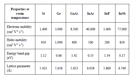
We could also think of using III-V heterostructures on IV-IV substrates for the channel engineering of future technology nodes nMOS transistors, in order to profit from the electron mobilities which are much higher than in column IV semiconductors [DEW 08, HUD 07, RAD 09]. As an example, we will find in Table 4.1 the electrons and the holes mobilities, the energy band gap, as well as the lattice parameter characteristic of various sphalerite and diamond semiconductors. The hole mobility is by far the most important in Ge. However, significant electron mobility gains (by a factor of 20 going from Ge to InSb!) could theoretically be obtained with III-V semiconductors as the channel material in nMOS transistors.
These heterostructures could be deposited in metallo-organic CVD [BRA 08, CHI 04], as well as in MBE [TAN 06] on Ge thick layers on Si, on Si1-xGex virtual substrates (typically x = 0.96) or on GeOI substrates. Hetero-junction bipolar transistors (HBT) and high electron mobility transistors based on AlGaAs and InP have recently been fabricated on top of GeSi and GeOI [LEW 07, LIU 09, LUB 08]. They have performances close to those obtained respectively on GaAs and InP substrates. High optical quality III-V heterostructures have otherwise been obtained on these Ge rich substrates, as mentioned in section 4.7. The pseudomorphic growth of heterostructures based on Ga(NAsP) alloys on Si substrates is most interesting for the Si photonics [KUN 10]. We could indeed consider a monolithic integration of III-V laser sources on IV-IV substrates, instead of using a complex flip-chip method [CAM 07].
As far as prospects are concerned, we should not forget subtle refinements regarding the selective or blanket epitaxy of {n-type doped Si / boron-doped SiGeC / n-type doped Si} heterostructures on patterned substrates, in order to form the core of HBT [CHE 09b, DEC 09, DUT 07, DUV 07]. The scopes of the hetero-epitaxy are indeed tremendous.
4.10. Bibliography
[ABB 06] ABBADIE A., HARTMANN J.M., DI NARDO C., BILLON T., CAMPIDELLI Y, BESSON P., Microelectronic Engineering, vol. 83, p. 1986, 2006.
[ABB 07a] ABBADIE A., HARTMANN J.M., BRUNIER F., ECS Transactions, vol. 10, no. 1, 2007.
[ABB 07b] ABBADIE A., BEDELL S.W., HARTMANN J.M., SADANA D.K., BRUNIER F., FIGUET C., CAYREFOURCQ I., Journal of the Electrochemical Society, vol. 154, H713, 2007.
[ABB 07c] ABBADIE A., HARTMANN J.M., CHERKASHIN N., DEGUET C., SANCHEZ L., BRUNIER F., LETERTRE F., ECS Transactions, vol. 6, no. 4, 263, 2007.
[ABB 08] ABBADIE A., HARTMANN J.M., BESSON P., ROUCHON D., MARTINEZ E., HOLLIGER P., DI NARDO C., LARDIN T., CAMPIDELLI Y., GHYSELEN B., BILLON T., Applied Surface Science, vol. 254, p. 6793, 2008.
[AEL 04] AELLA P., COOK C., TOLLE J., ZOLLNER S., CHIZMESHYA A.V.G., KOUVETAKIS J., Applied Physics Letters, vol. 84, p. 888, 2004.
[AKA 06a] AKATSU T. et al., ECS Transactions, vol. 3, no. 6, 107, 2006.
[AKA 06b] AKATSU T. et al., Material Science in Semiconductor Processing, vol. 9, p. 444, 2006.
[AND 03] ANDRIEU F. et al., Proceedings of the ESSDERC Conference, p. 267, 2003.
[AND 05a] ANDRE C.L., WILT D.M., PITERA A.J., LEE M.L., FITZGERALD E.A., RINGEL S.A., Journal of Applied Physics, vol. 98, 014502, 2005.
[AND 05b] ANDRIEU F. et al., Proceedings of the SOI Conference, p. 223, 2005.
[AND 06] ANDRIEU F. et al., Proceedings of the VLSI Technology Symposium, p. 168, 2006.
[AND 07] ANDRIEU F. et al., Proceedings of the VLSI Technology Symposium, p. 50, 2007.
[ANG 05] ANG K.W., CHUI K.J., BLIZNETSOV V., TANG C.H., DU A., BALASUBRAMIAN N., SAMUDRA G., LI M.F., YEO Y.C., Applied Physics Letters 86, 093102, 2005.
[AUG 09] AUGENDRE E. et al., ECS Transactions, vol. 25, no. 7, 351, 2009.
[BAB 02] BABOUX N., DUPUY J.C., PRUDON G., HOLLIGER P., LAUGIER F., PAPON A.M., HARTMANN J.M., Journal of Crystal Growth, vol. 245, no. 1, 2002.
[BAD 03] BADEL X., LINNROS J., KLEIMANN P., Electrochemical and Solid-State Letters, vol. 6, C79, 2003.
[BAR 08] BARNOLA S. et al., ECS Transactions, vol. 16, no. 10, 923, 2008.
[BAR 03] BARON T., PELISSIER B., PERNIOLA L., MAZEN F., HARTMANN J.M., ROLLAND G., Applied Physics Letters, vol. 83, p. 1444, 2003.
[BAR 07] BARRAL V. et al., Proceedings of the IEDM Conference, p. 61, 2007.
[BAS 01] BASCHIR R., CHAO K.-J., KABIR A.E., Journal of Vacuum Science and Technology B19, p. 517, 2001.
[BAT 07] BATAIL E. et al., Proceedings of the ESSDERC Conference, p. 450, 2007.
[BAT 08] BATAIL E. et al., Proceedings of the IEDM Conference, p. 397, 2008.
[BAT 09a] BATUDE P. et al., Proceedings of the IEDM Conference, p. 345, 2009.
[BAT 09b] BATUDE P. et al., Proceedings of the VLSI Technology Symposium, p. 166, 2009.
[BAU 06] BAUER M., ARENA C., BERTRAM R., TOMASINI P., CODY N., BRABANT P., ITALIANO J., JACOBSON P., WEEKS K.D., US Patent 2006/0234504 A1, 2006.
[BAU 07] BAUER M., MACHKAOUTSAN V., ARENA C., Semiconductor Sciences and Technology, vol. 22, S183, 2007.
[BED 04] BEDELL S.W., FOGEL K., SADANA D.K., CHEN H., DOMENICUCCI A., Applied Physics Letters, vol. 85, 2493, 2004.
[BER 08] BERNARD E. et al., Proceedings of the VLSI Technology Symposium, p. 16, 2008.
[BER 09a] BERNARD E., ERNST T., GUILLAUMOT B., VULLIET N., CORONEL P., SKOTNICKI T., DELEONIBUSS., FAYNOT O., IEEE Transactions on Electron Devices, vol. 56, p. 1243 and 1252, 2009.
[BER 09b] BERNARD E., ERNST T., GUILLAUMOT B., VULLIET N., LIM T.CH., ROZEAU O., DANNEVILLE F., CORONEL P., SKOTNICKI T., IEEE Electron Device Letters, vol. 30, p. 148, 2009.
[BID 08] BIDAL G.et al., Proceedings of the VLSI Technology Symposium, p. 146, 2008.
[BID 09a] BIDAL G. et al., Solid-State Electronics, vol. 53, p. 735, 2009.
[BID 09b] BIDAL G. et al., Proceedings of the IEDM Conference, p. 677, 2009.
[BOD 97] BODNAR S., DE BERRANGER E., BOUILLON P., MOUIS M., SKOTNICKI T., REGOLINI J.L., Journal of Vacuum Science and Technology B15, p. 712, 1997.
[BOE 08] DE BOER W.B., ECS Transactions, vol. 16, no. 10, 13, 2008.
[BOG 04] BOGUMILOWICZ Y., HARTMANN J.M., LAUGIER F., ROLLAND G., BILLON T., RENARD V., OLSHANETSKY E.B., ESTIBALS O., KVON Z.D., PORTAL J.C., Materials Research Society Symposium Proceedings, vol. 809, B1.9.1, 2004.
[BOG 05a] BOGUMILOWICZ Y., HARTMANN J.M., ROLLAND G., BILLON T., Journal of Crystal Growth, vol. 274, p. 28, 2005.
[BOG 05b] BOGUMILOWICZ Y., HARTMANN J.M., LAUGIER F., ROLLAND G., BILLON T., Solid State Phenomena, vol. 108–109, p. 445, 2005.
[BOG 05c] BOGUMILOWICZ Y., HARTMANN J.M., TRUCHE R., CAMPIDELLI Y., ROLLAND G., BILLON T., Semiconductor Science and Technology, vol. 20, p. 127, 2005.
[BOG 05d] BOGUMILOWICZ Y., HARTMANN J.M.,CHERKASHIN N., CLAVERIE A., ROLLAND G., BILLON T., Materials Science and Engineering B 124–125, p. 113, 2005.
[BOG 05e] BOGUMILOWICZ Y., HARTMANN J.M., TRUCHE R., CAMPIDELLI Y., ROLLAND G., BILLON T., Semiconductor Science and Technology, vol. 20, p. 127, 2005.
[BOG 06a] BOGUMILOWICZ Y., HARTMANN J.M., DI NARDO C., HOLLIGER P., PAPON A.M., ROLLAND G., BILLON T., Journal of Crystal Growth, vol. 290, p. 523, 2006.
[BOG 06b] BOGUMILOWICZ Y. et al., ECS Transactions, vol. 3, no. 7, 1099, 211, 2006.
[BOG 06c] BOGUMILOWICZ Y., HARTMANN J.M., FABBRI J.M., BILLON T., Semiconductor Science and Technology, vol. 21, p. 1668, 2006.
[BOR 06] BOREL S., CAUBET V., BILDE J., CHERIF A., ARVET C., VIZIOZ C., HARTMANN J.M., RABILLÉ G., BILLON T., ECS Transactions, vol. 3, no. 7, 627, 2006.
[BOU 04] BOUCAUD P., EL KURDI M., HARTMANN J.M., Applied Physics Letters, vol. 85, p. 46, 2004.
[BRA 08] BRAMMERTZ G., CAYMAX M., MEURIS M., HEYNS M., MOLS Y., DEGROOTE S., LEYS F., Thin Solid Films, vol. 517, p. 148, 2008.
[BRU 00] BRUNHES T., BOUCAUD P., SAUVAGE S., ANIEL F., LOURTIOZ J.M., HERNANDEZ C., CAMPIDELLI Y., KERMARREC O., BENSAHEL D., FAINI G., SAGNES I., Applied Physics Letters, vol. 77, p. 1822, 2000.
[CAM 07] VAN CAMPENHOUT J., ROJO-ROMEO P., REGRENY P., SEASSAL C., VAN THOURHOUT D., VERSTUYFT S., DI CIOCCI L., FEDELI J.M., LAGAHE C., BAETS R., Optics Express, vol. 15, p. 6744, 2007.
[CAU 06] CAUBET V., BEYLIER C., BOREL S., RENAULT O., Journal of Vacuum Science and Technology B 24, p. 2748, 2006.
[CHA 87] CHANG S., UNZICKER D., ANDERSON T.J., Proceedings of the 10th International Conference on CVD, vol. 87–8, p. 122, 1987.
[CHE 02] CHEN H., LI Y.K., PENG C.S., LIU H.F., LIU Y.L., HUANG Q., ZHOU J.M., XUE Q.K., Physics Review B 65, p. 233303, 2002.
[CHE 09a] CHENG K. et al., Proceedings of the VLSI Technology Symposium, p. 212, 2009.
[CHE 06] CHERKASHIN N., HŸTCH M.J., SNOECK E., HÜE F., HARTMANN J.M., BOGUMILOWICZ Y., CLAVERIE A., Nuclear Instruments and Methods in Physics Research B 253, p. 145, 2006.
[CHE 09b] CHEVALIER P. et al., Bipolar/BiCMOS Circuits and Technology Meeting, p. 1, 2009.
[CHI 04] CHRIQUI Y., LARGEAU L., PATRIARCHE G., SAINT-GIRONS G., BOUCHOULE S., SAGNES I., BENSAHEL D., CAMPIDELLI Y., KERMARREC O., Journal of Crystal Growth, vol. 265, p. 53, 2004.
[CHO 06] CHOPRA S., OZTURK M.C., MISRA V., MCGUIRE K., MCNEIL L.E., Applied Physics Letters, vol. 88, p. 202114, 2006.
[CHU 08] CHUNG K.H., YAO N., BENZIGER J., STURM J.C., SINGH K.K., CARLSON D., KUPPURAO S., Applied Physics Letters, vol. 92, no. 113, p. 506, 2008.
[CHU 98] CHURCHILL A.C., ROBBINS D.J., WALLIS D.J., GRIFFIN N., PAUL D.J., PIDDUCK A.J., LEONG W.Y., WILLIAMS G.M., Journal of Vacuum Science and Technology B 16, p. 1634, 1998.
[CIA 03] CIAMPOLINI L., BERTIN F., HARTMANN J.M., ROCHAT N., HOLLIGER P., LAUGIER F., CHABLI A., Materials Science and Engineering B 102, p. 113, 2003.
[CLA 07] CLAEYS C., SIMOEN E., Germanium-based Technologies: From Materials to Devices, Elsevier, Oxford, 2007.
[CLA 06] CLAVELIER L. et al., ECS Transactions, vol. 3, no. 7, p. 789, 2006.
[COL 98] COLACE L., MASINI G., GALLUZZI F., ASSANTO G., CAPELLINI G., DI GASPARE L., PELANGE E., EVANGELISTI F., Applied Physics Letters, vol. 72, p. 3175, 1998.
[COL 03] COLLAERT N., VERHEYEN P., DE MEYER K., LOO R., CAYMAX M., Solid-State Electronics, vol. 47, p. 1173, 2003.
[COL 06] COLLAERT N., ROOYACKERS R., CLEMENTE F., ZIMMERMAN P., CAYREFOURCQ I., GHYSELEN B., SAN K.T., JURCZAK M., BIESEMANS S., Proceedings of the VLSI Technology Symposium, p. 64, 2006.
[COO 07] COOPER D., TRUCHE R., RIVALLIN P., HARTMANN J.M., LAUGIER F., BERTIN F., CHABLI A., ROUVIÈRE J.L., Applied Physics Letters, vol. 91, p. 143501, 2007.
[COO 08] COOPER D., AILLIOT C., TRUCHE R., BARNES J.P., HARTMANN J.M., BERTIN F., Journal of Applied Physics, vol. 104, p. 064513, 2008.
[COO 09] COOPER D., RIVALLIN P., HARTMANN J.M., CHABLI A., DUNIN-BORKOWSKI R.E., Journal of Applied Physics, vol. 106, 06 4506, 2009.
[COO 10] COOPER D., BÉCHÉ A., HARTMANN J.M., CARRON V., ROUVIÈRE J.L., Journal of Applied Physics, vol. 96, 113508, 2010.
[CRE 06] CRESSLER J.D. (ed.), Silicon Heterostructure Handbook: Materials, Fabrication, Devices, Circuits and Applications of SiGe and Si Strained-Layer Epitaxy, CRC Press, Taylor & Francis Group, Boca Raton, 2006.
[CUR 98] CURRIE M.T., SAMAVEDAM S.B., LANGDO T.A., LEITZ C.W., FITZGERALD E.A., Applied Physics Letters, vol. 78, p. 1718, 1998.
[CUR 01] CURRIE M.T., LEITZ C.W., LANGDO T.A., TARASCHI G., FITZGERALD E.A., ANTONIADIS D.A., Journal of Vacuum Science and Technology B 19, p. 2268, 2001.
[DAM 04a] DAMLENCOURT J.F., WEBER O., RENAULT O., HARTMANN J.M., POGGI C., DUCROQUET F., BILLON T., Journal of Applied Physics, vol. 96, p. 5478, 2004.
[DAM 04b] DAMLENCOURT J.F., VANDELLE B., CLUZEL B., CALVO V., HARTMANN J.M., DAVID S., FÉDÉLI J.M., BILLON T., Electrical Society Proceedings, vol. 2004–07, p. 1033, 2004.
[DAM 10] DAMLENCOURT J.F., ECS Transactions, vol. 28, no. 1, p. 343, 2010.
[DEC 09] DECOUTERE S., VAN HUYLENBROECK S., HEINEMANN B., FOX A., CHEVALIER P., CHANTRE A., MEISTER T.F., AUFINGER K., SCHRÖTER M., Bipolar / BiCMOS Circuits and Technology Meeting, p. 16, 2009.
[DEL 04] DELHOUGNE R., ENEMAN G., CAYMAX M., LOO R., MEUNIER-BEILLARD P., VERHEYEN P., VANDERVORST W., DE MEYER K., HEYNS M., Solid-State Electronics, vol. 48, p. 1307, 2004.
[DES 07] DESTEFANIS V., MORAND Y., HARTMANN J.M., ROUCHON D., BARBÉ J.C., MERMOUX M., Applied Surface Science, vol. 254, p. 1436, 2007.
[DES 08a] DESTEFANIS V., HARTMANN J.M., BOREL S., BENSAHEL D., Semiconductor Science and Technology, vol. 23, p. 105019, 2008.
[DES 08b] DESTEFANIS V., HARTMANN J.M., HÜE F., BENSAHEL D., ECS Transactions, vol. 16, no. 10, 427, 2008.
[DES 08c] DESTEFANIS V., HARTMANN J.M., HOPSTAKEN M., DELAYE V., BENSAHEL D., Semiconductor Science and Technology, vol. 23, 105018, 2008.
[DES 10] DESTEFANIS V. et al., Semiconductor Science and Technology, vol. 25, p. 045014, 2010.
[DEW 08] DEWEY G., HUDAIT M.K., LEE K., PILLARISETTY R., RACHMADY W., RADOSAVLJEVIC M., RAKSHIT T., CHAU R., IEEE Electron Device Letters, vol. 29, p. 1094, 2008.
[DIM 07] DIMOULAS A., GUSEV E., MCINTYRE P.C., HEYNS M. (eds), Advanced Gate Stacks for High-Mobility Semiconductors, Springer, Berlin Heidelberg, 2007.
[DOR 07] DORNEL E., ERNST T., BARBÉ J.C., HARTMANN J.M., DELAYE V., AUSSENAC F., VIZIOZ C., BOREL S., MAFFINI-ALVARO V., ISHEDEN C., FOUCHER J., Applied Physics Letters, vol. 91, p. 233502, 2007.
[DUC 04a] DUCROQUET F., ERNST T., WEBER O., HARTMANN J.M., LOUP V., BESSON P., BRÉVARD L., DI MARIA J.L., DELEONIBUS S., Applied Surface Science, vol. 224, p. 274, 2004.
[DUC 04b] DUCROQUET F. et al., Proceedings of the IEDM Conference, p. 437, 2004.
[DUC 06] DUCROQUET F., HARTMANN J.M., TABONE C., LAFOND D., VIZIOZ C., ERNST T., DELEONIBUS S., ECS Transactions, vol. 3, no. 2, 333, 2006.
[DUP 08a] DUPRÉ C., ERNST T., MAFFINI-ALVARO V., DELAYE V., HARTMANN J.M., BOREL S., VIZIOZ C., FAYNOT O., GHIBAUDO G., DELEONIBUS S., Solid-State Electronics, vol. 52, p. 519, 2008.
[DUP 08b] DUPRÉ C. et al., Proceedings of the IEDM Conference, p. 749, 2008.
[DUT 91] DUTARTRE D., BRÉMOND G., SOUIFI A., BENYATTOU T., Physics Review B, vol. 44, p. 11525, 1991.
[DUT 07] DUTARTRE D., LOUBET N., BROSSARD F., VANDELLE B., CHEVALIER P.,CHANTRE A., MONFRAY S., FENOUILLET-BERANGER C., POUYDEBASQUE A., SKOTNICKI T., Proceedings of the IEDM Conference, p. 689, 2007.
[DUV 07] DUVERNAY J., BOROT G., CHEVALIER P., DUTARTRE D., PANTEL R.,RUBALDO L.,SCHWARTZMANN T., VANDELLE B., CHANTRE A., Proceedings of the ESSDERC Conference, p. 346, 2007.
[EAG 91] EAGLESHAM D.J., CERULLO M., Applied Physics Letters, vol. 58, p. 2276, 1991.
[ERD 05] ERDTMANN M., CURRIE M.T., WOICIK J.C., BLACK D., Materials Research Society Symposium Proceedings, p. 891, EE12-05, 2005.
[ERN 02] ERNST T. et al., Proceedings of the VLSI Technology Symposium, p. 92–93, 2002.
[ERN 03] ERNST T. et al., Proceedings of the VLSI Technology Symposium, p. 51–52, 2003.
[ERN 09] ERNST T. et al., ECS Transactions, vol. 25, no. 7, 471, 2009.
[FAN 07] FANG Y.Y., TOLLE J., ROUCKA R., CHIZMESHYA A.V.G., KOUVETAKIS J., D’COSTA V., MENÉNDEZ J., Applied Physics Letters, vol. 90, p. 061915, 2007.
[FIO 04] FIORENZA J.G. et al., Semiconductor Science and Technology, vol. 19, 2004.
[FIT 99] FITZGERALD E.A., CURRIE M.T., SAMAVEDAM S.B., LANGDO T.A., TARASCHI G., YANG V., LEITZ C.W., BULSARA M.T., Physica Status Solidi (a), vol. 171, p. 227, 1999.
[GHY 04] GHYSELEN B. et al., Solid-State Electronics, vol. 48, p. 1285, 2004.
[GIA 03] GIANNAKOPOULOS K.P., ROTH S., BURGHAMMER M., FELLOUS C., RICHARD D., DUTARTRE D., Journal of Applied Physics, vol. 93, p. 259, 2003.
[GON 08] GONZATTI F., HARTMANN J.M., YCKACHE K., ECS Transactions, vol. 16, no. 10, p. 485, 2008.
[GOU 09a] GOUYÉ A., KERMARREC O., HALIMAOUI A., CAMPIDELLI Y., ROUCHON D., BURDIN M., HOLLIGER P., BENSAHEL D., Journal of Crystal Growth, vol. 311, p. 3522, 2009.
[GOU 09b] GOUYÉ A., HÜE F., HALIMAOUI A., KERMARREC O., CAMPIDELLI Y., HŸTCH M.J., HOUDELLIER F., CLAVERIE A., BENSAHEL D., Material Science in Semiconductor Processing, vol. 12, p. 34, 2009.
[GUP 90] GUPTA P., COON P.A., KOELER B.G., GEORGES S.M., Journal of Chemical Physics, vol. 93, p. 2827, 1990.
[HAN 06] HAN J.P. et al., Proceedings of the IEDM Conference, p. 59, 2006.
[HAR 02a] HARTMANN J.M., LOUP V., ROLLAND G., HOLLIGER P., LAUGIER F., VANNUFFEL C., SÉMÉRIA M.N., Journal of Crystal Growth, vol. 236, p. 10, 2002.
[HAR 02b] HARTMANN J.M., CHAMPAY F., LOUP V., ROLLAND G., SÉMÉRIAM. N., Journal of Crystal Growth, vol. 241, p. 93, 2002.
[HAR 02c] HARTMANN J.M., ERNST T., LOUP V., DUCROQUET F., ROLLAND G., LAFOND D., HOLLIGER P., LAUGIER F., SÉMÉRIA M.N., DELEONIBUS S., Journal of Applied Physics, vol. 92, p. 2368, 2002.
[HAR 03a] HARTMANN J.M., ABBADIE A., VINET M., CLAVELIER L., HOLLIGER P., LAFOND D., SÉMÉRIA M.N., GENTILE P., Journal of Crystal Growth, vol. 257, p. 19, 2003.
[HAR 03b] HARTMANN J.M., LOUP V., ROLLAND G., SÉMÉRIA M.N., Journal of Vacuum Science and Technology B 21, p. 2524, 2003.
[HAR 03c] HARTMANN J.M., BERTIN F., ROLLAND G., LAUGIER F., SÉMÉRIA M.N., Journal of Crystal Growth, vol. 259, p. 419, 2003.
[HAR 04a] HARTMANN J.M., CLAVELIER L., JAHAN C., HOLLIGER P., ROLLAND G.,BILLON T., DEFRANOUX C., Journal of Crystal Growth, vol. 264, p. 36, 2004.
[HAR 04b] HARTMANN J.M., ERNST T., DUCROQUET F., ROLLAND G., LAFOND D., PAPON A.M., TRUCHE R., HOLLIGER P., LAUGIER F., SÉMÉRIA M.N., DELEONIBUS S., Semiconductor Science and Technology, vol. 19, p. 593, 2004.
[HAR 04c] HARTMANN J.M. et al., Semiconductor Science and Technology, vol. 19, p. 311, 2004.
[HAR 04d] HARTMANN J.M., ABBADIE A., PAPON A.M., HOLLIGER P., ROLLAND G., BILLON T., FÉDÉLI J.M., ROUVIÈRE M., VIVIEN L., LAVAL S., Journal of Applied Physics, vol. 95, p. 5905, 2004.
[HAR 04e] HARTMANN J.M., PAPON A.M., HOLLIGER P., ROLLAND G., BILLON T., ROUVIÈRE M., VIVIEN L., LAVAL S., Material Research Society Symposium Proceedings, vol. 809, B4.3.1, 2004.
[HAR 05a] HARTMANN J.M., BOGUMILOWICZ Y., ANDRIEU F., HOLLIGER P., ROLLAND G., BILLON T., Journal of Crystal Growth, vol. 277, p. 114, 2005.
[HAR 05b] HARTMANN J.M., HOLLIGER P., LAUGIER F., ROLLAND G., SUHM A., ERNST T., BILLON T., VULLIET N., Journal of Crystal Growth, vol. 283, p. 57, 2005.
[HAR 05c] HARTMANN J.M., BERTIN F., ROLLAND G., SÉMÉRIA M.N., BRÉMOND G., Thin Solid Films, vol. 479, p. 113, 2005.
[HAR 05d] HARTMANN J.M., DAMLENCOURT J.F., BOGUMILOWICZ Y., HOLLIGER P., ROLLAND G., BILLON T., Journal of Crystal Growth, vol. 274, p. 90, 2005.
[HAR 06a] HARTMANN J.M., BAUD L., ROLLAND G., FABBRI J.M., BILLON T., ECS Transactions, vol. 3, no. 7, 219, 2006.
[HAR 06b] HARTMANN J.M., PAPON A.M., FABBRI J.M., ROLLAND G., BILLON T., JUHEL M., HALIMAOUI A., ECS Transactions, vol. 3, no. 7, 489, 2006.
[HAR 06c] HARTMANN J.M., BURDIN M., ROLLAND G., BILLON T., Journal of Crystal Growth, vol. 294, p. 288, 2006.
[HAR 07a] HARTMANN J.M., Journal of Crystal Growth, vol. 305, p. 113, 2007.
[HAR 07b] HARTMANN J.M., ABBADIE A., GUINCHE Y., HOLLIGER P., ROLLAND G., BUISSON M., DEFRANOUX C., PIERREL F., BILLON T., Semiconductor Science and Technology, vol. 22, p. 354, 2007.
[HAR 07c] HARTMANN J.M., ABBADIE A., ROUCHON D., MERMOUX M., BILLON T., Semiconductor Science and Technology, vol. 22, p. 362, 2007.
[HAR 08a] HARTMANN J.M., GONZATTI F., FILLOT F., BILLON T., Journal of Crystal Growth, vol. 310, p. 62, 2008.
[HAR 08b] HARTMANN J.M., ANDRIEU F., LAFOND D., ERNST T., BOGUMILOWICZ Y., DELAYE V., WEBER O., ROUCHON D., PAPON A.M., Materials Science and Engineering B 154–155, p. 76, 2008.
[HAR 08c] HARTMANN J.M., ABBADIE A., ROUCHON D., BARNES J.P., MERMOUX M., BILLON T., Thin Solid Films 516, p. 4238, 2008.
[HAR 08d] HARTMANN J.M., BOGUMILOWICZ Y., ABBADIE A., FILLOT F., BILLON T., Journal of Crystal Growth, vol. 310, p. 249, 2008).
[HAR 08e] HARTMANN J.M., PAPON A.M., DESTEFANIS V., BILLON T., Journal of Crystal Growth, vol. 310, p. 5287, 2008.
[HAR 09a] HARTMANN J.M., PAPON A.M., BARNES J.P., BILLON T., Journal of Crystal Growth, vol. 311, p. 3152, 2009.
[HAR 09b] HARTMANN J.M., ABBADIE A., CHERKASHIN N., GRAMPEIX H., CLAVELIER L., Semiconductor Science and Technology, vol. 24, p. 055002, 2009.
[HAR 10a] HARTMANN J.M., SANCHEZ L., VAN DEN DAELE W., ABBADIE A., BAUD L., TRUCHE R., AUGENDRE E., CLAVELIER L., CHERKASHIN N., HŸTCH M., CRISTOLOVEANU S., Semiconductor Science and Technology, vol. 25, p. 075010, 2010.
[HAR 10b] HARTMANN J.M., ABBADIE A., BARNES J.P., FÉDÉLI J.M., BILLON T., VIVIEN L., Journal of Crystal Growth, vol. 312, p. 532, 2010.
[HAR 10c] HARTMANN J.M., PY M., MOREL P.H., ERNST T., PRÉVITALI B., BARNES J.P., VULLIET N., CHERKASHIN N., REBOH S., HŸTCH M., PAILLARD V., ECS Transactions, vol. 33, no. 7, 391, 2010.
[HER 99] HERNANDEZ C., CAMPIDELLI Y., SIMON D., BENSAHEL D., SAGNES I., PATRIARCHE G., BOUCAUD P., SAUVAGE S., Journal of Applied Physics, vol. 86, p. 1145, 1999.
[HER 03] HERNANDEZ C., CAMPIDELLI Y., BENSAHEL D., United States Patent 6, 537, 370 B1, 2003.
[HIK 09] HIKAVYY A., LOO R., WITTERS L., TAKEOKA S., GEYPEN J., BRIJS B., MERCKLING C., CAYMAX M., DEKOSTER J., ECS Transactions, vol. 25, no. 7, 201, 2009.
[HIR 05] HIRASHITA N., SUGIYAMA N., TOYODA E., TAGAKI S., Applied Physics Letters, vol. 86, p. 221923, 2005.
[HOL 10] HOLLÄNDER B., BUCA D., MANTL S., HARTMANN J.M., Journal of the Electrochemical Society, vol. 157, H643, 2010.
[HU 05a] HU C.W., TSONG I.S.T., D’COSTA V., MENÉNDEZ J., CROZIER P.A., TOLLE J., KOUVETAKIS J., Applied Physics Letters, vol. 87, p. 083101, 2005.
[HU 05b] HU C.W., MENÉNDEZ J., TSONG I.S.T., TOLLE J., CHIZMESHYA A.V.G., RITTER R., KOUVETAKIS J., Applied Physics Letters, vol. 87, p. 181903, 2005.
[HUA 98] HUANG J., YE Y.Z., LU H., QUE D., Journal of Applied Physics, vol. 83, p. 171, 1998.
[HUB 08] HUBERT A. et al., ECS Transactions, vol. 13, no. 1, 195, 2008.
[HUD 07] HUDAIT M.K. et al., Proceedings de la conférence IEDM, p. 625, 2007.
[HUE 07] HÜE F., HŸTCH M., BENDER H., HARTMANN J.M., CLAVERIE A., Material Research Symposium Proceedings, vol. 1026E,1026-C20-04, 2007.
[HUE 08] HÜE F., HŸTCH M., BENDER H., HOUDELLIER F., CLAVERIE A., Physical Review Letters, vol. 100, p. 156602, 2008.
[HUE 09] HÜE F., HŸTCH M., HOUDELLIER F., BENDER H., CLAVERIE A., Applied Physics Letters, vol. 95, p. 073103, 2009.
[HUT 10a] HUTIN L. et al., Proceedings of the IEDM Conference, p. 253, 2010.
[HUT 10b] HUTIN L., LE ROYER C., DAMLENCOURT J.F., HARTMANN J.M., GRAMPEIX H., MAZZOCCHI V., TABONE C., PREVITALI B., POUYDEBASQUE A., VINET M., FAYNOT O., IEEE Electron Device Letters, vol. 31, p. 234, 2010.
[ISH 02] ISHIKAGAWA Y., KUMEZAWA M., NURYADI R., TABE M., Applied Surface Science, vol. 190, p. 11, 2002.
[ITO 95] ITOH S., NAKAMURA T., NISCHIKAWA S., Journal of Applied Physics, vol. 78, p. 2716, 1995.
[JAH 05] JAHAN C., FAYNOT O., TOSTI L., HARTMANN J.M., Journal of Crystal Growth, vol. 280, p. 530, 2005.
[JOS 07] JOSHIL S. et al., Proceedings of the DRC Conference, p. 53, 2007.
[KAM 97] KAMINS T.I., CARR E.C., WILLIAM R.S., ROSNER S.J., Journal of Applied Physics, vol. 81, p. 211, 1997.
[KAM 98] KAMINS T.I., BRIGGS G.A.D., STANLEY WILLIAMS R., Applied Physics Letters, vol. 73, p. 1862, 1998.
[KAM 03] KAMINS T.I., MEIDEIROS-RIBEIRO G., OHLBERG D.A.A., STANLEY WILLIAMS R., Journal of Applied Physics, vol. 94, p. 4215, 2003.
[KAS 00] KASPAR E., LYUTOUICH K., Properties of Silicon Germanium and SiGe:Carbon, INSPEC, The Institution of Electrical Engineers, London, 2000.
[KER 04] KERMARREC O., CAMPIDELLI Y., BENSAHEL D., Journal of Applied Physics, vol. 96, p. 6175, 2004.
[KIM 06] KIMURA Y., SUGII N., KIMURA S., INUI K., HIRASAWA W., Applied Physics Letters, vol. 88, p. 031912, 2006.
[KOL 09] KOLAHDOUZ M., MARESCA L., OSTLING M., RILEY D., WISE R., RADAMSON H.H., Solid-State Electronics 53, 858, 2009.
[KON 97] KONGETIRA P., NEUDECK G., TAKOUDIS C.G., Journal of Vacuum Science and Technology B 15, 1902, 1997.
[KOU 08] KOUVETAKIS J., TOLLE J., ROUCKA R., D’COSTA V., FANG Y.Y., CHIZMESHYA A.V.G., MENÉNDEZ J., ECS Transactions, vol. 16, no. 10, 807, 2008.
[KNU 94] KNUTSON K.L., CARR R.W., LIU W.H., CAMPBELL S.A., Journal of Crystal Growth, vol. 140, p. 191, 1994.
[KUN 10] KUNERT B., VOLZ K., STOLZ W., ECS Transactions, vol. 28, no. 5, 219, 2010.
[KUR 02a] EL KURDI M., BOUCAUD P., SAUVAGE S., KERMARREC O., CAMPIDELLI Y., BENSAHEL D., SAINT-GIRONS G., SAGNES I., Applied Physics Letters, vol. 80, p. 509, 2002.
[KUR 02b] EL KURDI M., BOUCAUD P., SAUVAGE S., FISHMAN G., KERMARREC O., CAMPIDELLI Y., BENSAHEL D., SAINT-GIRONS G., SAGNES I., PATRIARCHE G., Journal of Applied Physics, vol. 92, p. 1858, 2002.
[KWO 06] KWON O., BOECKL J.J., LEE M.L., PITERA A.J., FITZGERALD E.A., RINGEL S.A., Journal of Applied Physics, vol. 100, p. 013103, 2006.
[LAU 04] LAUGIER F., HARTMANN J.M., MORICEAU H., HOLLIGER P., TRUCHE R., DUPUY J.C., Applied Surface Science, vol. 231–232, p. 668, 2004.
[LEE 04] LEE M.L., PITERA A.J., FITZGERALD E.A., Journal of Vacuum Science and Technology B 22, p. 158, 2004.
[LEI 01] LEITZ C.W., CURRIE M.T., KIM A.Y., LAI J., ROBBINS E., FITZGERALD E.A., Journal of Applied Physics, vol. 90, p. 2730, 2001.
[LEI 02] LEITZ C.W., CURRIE M.T., LEE M.L., CHENG Z.Y., ANTONIADIS D.A., FITZGERALD E.A., Journal of Applied Physics, vol. 92, p. 3745, 2002.
[LEW 07] LEW K.L., YOON S.F., LOKE W.K., TANATO H., DOHRMAN C.L., ISAACSON M., FITZGERALD E.A., Journal of Vacuum Science and Technology B 25, p. 902, 2007.
[LIU 09] LIU W.K. et al., Journal of Crystal Growth, vol. 311, p. 1979, 2009.
[LIU 10] LIU J., SUN X., CAMACHO-AGUILERA R., KIMERLING L.C., MICHEL J., Optics Express, vol. 35, p. 679, 2010.
[LOO 01] LOO R., MEUNIER-BEILLARD P., VANHAEREN D., BENDER H., CAYMAX M., VANDERVORST W., DENTEL D., GORYLL M., VESCAN L., Journal of Applied Physics, vol. 90, p. 2565, 2001.
[LOU 02] LOUP V., HARTMANN H.M., ROLLAND G., HOLLIGER P., LAUGIER F., VANNUFFEL C., SÉMÉRIA M.N., Journal of Vacuum Science and Technology B 20, p. 1048, 2002.
[LOU 03a] LOUP V., HARTMANN J.M., ROLLAND G., HOLLIGER P., LAUGIER F., SÉMÉRIA M.N., Journal of Vacuum Science and Technology B 21, p. 246, 2003.
[LOU 03b] LOUP V., HARTMANN J.M., ROLLAND G., HOLLIGER P., LAUGIER F., LAFOND D., SÉMÉRIA M.N., BESSON P., GENTILE P., Semiconductor Science and Technology, vol. 18, p. 352, 2003.
[LUA 99] LUAN H.C., LIM D.R., LEE K.K., CHEN K.M., SANDLAND J., WADA K., KIMERLING L.C., Applied Physics Letters, vol. 75, p. 2909, 1999.
[LUB 08] LUBYSHEV D., FASTENAU J.M., WU Y., LIU W.K., BULSARA M.T., FITZGERALD E.A., HOKE W.E., Journal of Vacuum Science and Technology B 26, p. 1115, 2008.
[MAR 09] MARRIS-MORINI D. et al., Proceedings of the IEEE 97, p. 1199, 2009.
[MAS 03] MASAROTTO L., HARTMANN J.M., BRÉMOND G., ROLLAND G., PAPON A.M., SÉMÉRIA M.N., Journal of Crystal Growth, vol. 255, p. 8, 2003.
[MAZ 03a] MAZEN F., BARON T., HARTMANN J.M., BRÉMOND G., SÉMÉRIA M.N., Journal of Crystal Growth, vol. 255, p. 250, 2003.
[MAZ 03b] MAZEN F., BARON T., PAPON A.M., TRUCHE R., HARTMANN J.M., Applied Surface Science, vol. 214, p. 359, 2003.
[MAZ 04a] MAZEN F., MOLLARD L., BARON T., DECOSSAS S., HARTMANN J.M., Microelectronic Engineering, vol. 73–74, p. 632, 2004.
[MAZ 04b] MAZEN F., BARON T., HARTMANN J.M., SÉMÉRIAM.N., US Patent 6, 946, 369 B2 (20 September 2005) and European Patent 1 426 328 A2, 2004.
[MEN 04] MENÉNDEZ J., KOUVETAKIS J., Applied Physics Letters, vol. 85, p. 1175, 2004.
[MEN 01] MENON C., BENTZEN A., RADAMSON H.H., Journal of Applied Physics, vol. 90, p. 4805, 2001.
[MEN 03] MENON C., LINDGREN A.-C., PERSSON P.O.A., HULTMAN L., RADAMSON H.H., Journal of the Electrochemical Society, vol. 150, G253, 2003.
[MER 10] MERMOUX M., CRISCI A., BAILLET F., DESTEFANIS V., ROUCHON D., PAPON A.M., HARTMANN J.M., Journal of Applied Physics, vol. 107, p. 013512, 2010.
[MI 95] MI J., WARREN P., LETOURNEAU P., JUDELEWICZ M., GAILHANOU M., DUTOIT M., DUBOIS C., DUPUY J.C., Applied Physics Letters, vol. 67, p. 259, 1995.
[MIS 07] MISTRY K. et al., Proceedings of the IEDM Conference, p. 247, 2007.
[MIT 09] MITARD J. et al., Proceedings of the VLSI Technology Symposium, p. 82, 2009.
[MIT 97] MITCHELL T.O., HOYT J.L., GIBBONS J.F., Applied Physics Letters, vol. 71, p. 1688, 1997.
[MIY 99] MIYANO K., MIZUSHIMA I., OHUCHI K., HOKAZANO A., TSUNASHIMA Y., Japanese Journal of Applied Physics, vol. 38, p. 2419, 1999.
[MO 90] MO Y.W., SAVAGE D.E., SCHWARTSENTRUBER B.S., LAGALLY M., Physical Review Letters, vol. 65, p. 1020, 1990.
[MOL 07] MOLAS G. et al., Proceedings of the IEDM Conference, p. 453, 2007.
[MON 07] MONFRAY S.et al., Proceedings of the IEDM Conference, p. 693, 2007.
[MON 10] MONFRAY S. et al., Solid-State Electronics, vol. 54, p. 90, 2010.
[MUN 08a] MUNGUÍA J., BREMOND G., BLUET J.M., HARTMANN J.M., MERMOUX M., Applied Physics Letter, vol. 93, p. 102101, 2008.
[MUN 08b] MUNGUÍA J., BLUET J.M., BAIRA M., MARTY O., BREMOND G., HARTMANN J.M., MERMOUX M., Applied Physics Letter, vol. 93, p. 191913, 2008.
[NGU 07] NGUYEN Q.T., DAMLENCOURT J.F., VINCENT B., CLAVELIER L., MORAND Y., GENTIL P., CRISTOLOVEANU S., Solid-State Electronics, vol. 51, p. 1172, 2007.
[OKA 07] OKAMOTO S. et al., Proceedings of the IEDM Conference, p. 277, 2007.
[ONO 95] ONO Y., NAGASE M., TABE M., TAKAHASHI Y., Japanese Journal of Applied Physics, vol. 34, p. 1728, 1995.
[OSM 09] OSMOND J., VIVIEN L., FÉDÉLI J.M., MARRIS-MORINI D., CROZAT P., DAMLENCOURT J.F., CASSAN E., LECUNFF Y., Applied Physics Letter, vol. 95, p. 151116, 2009.
[PAN 06] PAN J.W., LIU P.W., CHANG T.Y., CHIANG W.T., TSAI C.H., LIN Y.H., TSAI.C.T., MA G.H., CHIEN S.C., SUN S.W., Proceedings of the IEDM Conference, p. 1, 2006.
[POU 08] POUYDEBASQUE A. et al., Proceedings of the VLSI-TSA Symposium, p. 16, 2008.
[POU 09] POUYDEBASQUE A., ROMANJEK K., LE ROYER C., TABONE C., PREVITALI B., ALLAIN F.,AUGENDRE E.,HARTMANN J.M., GRAMPEIX H., VINET M., IEEE Transactions on Electron Devices, vol. 56, p. 3240, 2009.
[RAD 09] RADOSAVLJEVIC M. et al., Proceedings of the IEDM Conference, p. 319, 2009.
[REE 96] REEBER R.R., WANG K., Materials Chemistry and Physics, vol. 46, p. 259, 1996.
[RIM 03] RIM K.et al., Proceedings of the IEDM Conference, p. 49, 2003.
[ROB 91] ROBBINS D.J., GLASPER J.L., GULLIS A.G., LEONG W.Y., Journal of Applied Physics, vol. 69, p. 3729, 1991.
[ROB 92] ROBBINS D.J., GASPER J.L., CULLIS A.G., LEONG W.Y., Journal of Applied Physics, vol. 69, p. 3729, 1992.
[ROM 09] ROMANJEK K. et al., Microelectronics Engineering, vol. 86, p. 1585, 2009.
[ROU 08] ROUCHON D., HARTMANN J.M., CRISCI A., MERMOUX M., ECS Transactions, vol. 16, no. 10, 181, 2008.
[ROU 05] ROUCKA R., TOLLE J., COOK C., CHIZMESHYA A.V.G., KOUVETAKIS J., D’COSTA V., MENÉNDEZ J., CHEN Z.D., ZOLLNER S., Applied Physics Letters, vol. 86, p. 191192, 2005.
[ROU 07] ROUCKA R., TOLLE J., FORREST B., KOUVETAKIS J., D’COSTA V., MENÉNDEZ J., Journal of Applied Physics, vol. 101, p. 013518, 2007.
[ROU 06] ROUVIÈRE M., VIVIEN L., LE ROUX X., MANGENEY J., CROZAT P., HOARAU C., CASSAN E., PASCAL S., LAVAL S., FÉDÉLI J.M., DAMLENCOURT J.F., HARTMANN J.M., KOLEV S., Applied Physics Letters, vol. 87, p. 231109, 2005.
[ROY 08] LE ROYER C.et al., Solid-State Electronics, vol. 52, 1285, 2008.
[RUC 98] RÜCKER H., HEINEMANN B., RÖPKE W., KURPS R., KRÜGER D., LIPPERT G., OSTEN H.J., Applied Physics Letters, vol. 73, p. 1682, 1998.
[SAK 97] SAKAI A., TATSUMI T., AOYAMA K Applied Physics Letters, vol. 71, p. 3510, 1997.
[SAL 03] DE SALVO B. et al., Proceedings of the IEDM Conference, p. 26.1.1, 2003.
[SAL 08] SALVETAT T., DESTEFANIS V., BOREL S., HARTMANN J.M., KERMARREC O., CAMPIDELLI Y., ECS Transactions, vol. 16, no. 10, 439, 2008.
[SAR 09] SARACCO E. et al., ECS Transactions, vol. 19, no. 1, 207, 2009.
[SCH 97] SCHÄFFLER F., Semiconductor Science and Technology, vol. 12, p. 1515, 1997.
[SHA 05] SHANG H. et al., Proceedings of the VLSI Technology Symposium, p. 78, 2005.
[SHE 05] SHERAW C.D. et al., Proceedings of the VLSI Technology Symposium, p. 12, 2005.
[SIN 99] SINGH D.V., RIM K., MITCHELL T.O., HOYT J., GIBBONS J.F., Journal of Applied Physics, vol. 85, p. 978 and 985, 1999.
[SIN 89] SINNIAH K., SHERMAN M.G., LEWIS L.B., WEINBERG W.H., YATES JR. J.T., JANDA K.C., Physical Review Letters, vol. 62, p. 567, 1989.
[SUE 00] SUE K.Y., LEE H.H., Journal of Applied Physics, vol. 88, p. 404, 2000.
[SUG 05] SUGII N. et al., Proceedings of the VLSI Technology Symposium, p. 54, Kyoto, Japan, 2005.
[SUN 09] SUN X., LIU J., KIMERLING L.C., MICHEL J., Applied Physics Letters, vol. 95, p. 011911, 2009.
[SUR 84] SURNEV L., TIKHOV M., Surface Science, vol. 138, p. 40, 1984.
[TAC 09] TACHI K. et al., Proceedings of the IEDM Conference, p. 313, 2009.
[TAC 10] TACHI K. et al., Proceedings of the ESSDERC Conference, p. 368, 2010.
[TAK 10] TAKEUCHI S., NGUYEN N.D., GOOSENS J., CAYMAX M., LOO R., Thin Solid Films, vol. 518, S18, 2010.
[TAN 06] TANOTO H., YOON S.F., LOKE W.K., FITZGERALD E.A., DOHRMAN C., NARAYANAN B., DOAN M.T., TUNG C.H., Journal of Vacuum Science and Technology B 24, p. 152, 2006.
[THE 05a] THEAN A.V.Y. et al., Proceedings of the VLSI Technology Symposium, p. 134n Kyoton Japan, 2005.
[THE 05b] THEAN A.V.Y. et al., Proceedings of the IEDM Conference, p. 515, 2005.
[THE 06] THEAN A.V.Y. et al., Proceedings of the VLSI Technology Symposium, Honolulu, p. 164, 2006.
[THO 03] THOMAS S.G. et al., Journal of Electronic Materials, vol. 32, p. 976, 2003).
[THO 06] THOMPSON S.E., GUANGYU S., YOUN SUNG C., NISHIDA T., IEEE Transactions on Electron Devices, vol. 53, p. 1010, 2006.
[TOL 06a] TOLLE J., ROUCKA R., CHIZMESHYA A.V.G., KOUVETAKIS J., D’COSTA V., MENÉNDEZ J., Applied Physics Letters, vol. 88, p. 252112, 2006.
[TOL 06b] TOLLE J., CHIZMESHYA V.G., FANG Y.Y., KOUVETAKIS J., D’COSTA V., HU C.W., MENÉNDEZ J., TSONG I.S.T., Applied Physics Letters, vol. 89, p. 231924, 2006.
[VIN 05] VINET M. et al., IEEE Electron Device Letters, vol. 26, p. 317, 2005.
[VIN 10] VINET M., LE ROYER C., BATUDE P., DAMLENCOURT J.F., HARTMANN J.M., HUTIN L., ROMANJEK K., POUYDEBASQUE A., THOMAS O., International Journal of Nanotechnology, vol. 7, p. 304, 2010.
[VIV 07] VIVIEN L. et al., Optics Express, vol. 15, p. 9843, 2007.
[VIV 09] VIVIEN L., OSMOND J., FÉDÉLI J.M., MARRIS-MORINI D., CROZAT P., DAMLENCOURT J.F., CASSAN E., LECUNFF Y., LAVAL S., Optics Express, vol. 17, p. 6252, 2009.
[VYA 02] VYATKIN A., STARKOV V., TZEITLIN V., PRESTING H., KONLE J., KÖNIG U., Journal of the Electrochemical Society, vol. 149, G70, 2002.
[WAL 86] WALLE C.G., MARTIN R.M., Physical Review B 34, p. 5621, 1986.
[WEB 03] WEBER O. et al., Proceedings of the ESSDERC Conference, p. 271, 2003.
[WEB 04a] WEBER O. et al., Proceedings of the VLSI Technology Symposium, p. 42–43, 2004.
[WEB 04b] WEBER O. et al., Proceedings of the IEDM Conference, p. 867, 2004.
[WEB 05] WEBER O. et al., Proceedings of the IEDM Conference, p. 143, 2005.
[WES 04] WESTHOFF R., CARLIN J., ERDTMANN M., LANGDO T.A., LEITZ C.W., YANG V., PETROCELLI K., BULSARA M.T., FITZGERALD E.A., VINEIS C.J., Electrochemical Society Proceedings, vol. 2004–07, p. 589, 2004.
[WHA 98] WHALL T.E., PARKER C.H.E., Journal of Physics D: Applied Physics, vol. 31, p. 1397, 1998.
[WIS 07] WISTLEY M.A., FANG Y.Y., TOLLE J., CIZMESHYA A.V.G., KOUVETAKIS J., Applied Physic Letters, vol. 90, 082, 108, 2007.
[YAN 00] YANG J., NEUDECK G.W., DENTON J.P., Applied Physic Letters, vol. 77, p. 4034, 2000.
[YAN 08] YANG B. et al., Proceedings of the IEDM Conference, 2008.
[YIN 06] YIN H. et al., Proceedings of the VLSI Technology Symposium, Honolulu, USA, p. 94, 2006.
[ZHA 06] ZHANG P., ISTRATOV A.A., WEBER E.R., KISIELOWSKI C., HE H., NELSON C., SPENCE J.C.H., Applied Physics Letters, vol. 89, p. 161907, 2006.
1Chapter written by Jean-Michel HARTMANN.