
6
Output Deviations-Based SDD Testing
Yilmaz Mahmut
6.2 The Need for Alternative Methods
6.3 Probabilistic Delay Fault Model and Output Deviations for SDDs
6.3.1 Method of Output Deviations
6.3.1.1 Gate Delay Defect Probabilities
6.3.1.2 Propagation of Signal Transition Probabilities
6.3.1.3 Implementation of Algorithm for Propagating Signal Transition Probabilities
6.3.1.4 Pattern-Selection Method
6.3.2 Practical Aspects and Adaptation to Industrial Circuits
6.3.3 Comparison to SSTA-Based Techniques
6.4.1 Experimental Setup and Benchmarks
6.4.3 Comparison of the Original Method to the Modified Method
6.1 Introduction
Very deep-submicron (VDSM) process technologies are leading to increasing densities and higher clock frequencies for integrated circuits (ICs). However, VDSM technologies are susceptible to process variations, crosstalk noise, power supply noise, and defects such as resistive shorts and opens, which induce small-delay variations in the circuit components. The literature refers to such delay variations as small-delay defects (SDDs) [Ahmed 2006b].
Although the delay introduced by each SDD is small, the overall impact might be significant if the target path is critical, has low slack, or includes many SDDs. The overall delay of the path might become longer than the clock period, causing circuit failure or temporarily incorrect results. As a result, the detection of SDDs requires fault excitation through least-slack paths. The longest paths in the circuit, except false paths and multicycle paths, are referred to as the least-slack paths.
6.2 The Need for Alternative Methods
The transition delay fault (TDF) [Waicukauski 1987] model attempts to propagate the lumped-delay defect of a gate by logical transitions to the observation points or state elements. The TDF model is not effective for SDDs because test generation using TDFs leads to the excitation of short paths [Ahmed 2006b; Forzan 2007]. Park et al. first proposed a statistical method for measuring the effectiveness of delay fault automatic test pattern generation (ATPG) [Park 1989]. The proposed technique is especially relevant today, and it can handle process variations on sensitized paths; however, this work is limited in the sense that it only provides a metric for delay test coverage, and it does not aim to generate or select effective patterns.
Due to the growing interest in SDDs, vendors recently introduced the first commercial timing-aware ATPG tools (e.g., new versions of Mentor Graphics FastScan, Cadence Encounter Test, and Synopsys TetraMax). These tools attempt to make ATPG patterns more effective for SDDs by exercising longer paths or applying patterns at higher-than-rated clock frequencies. However, only a limited amount of timing information is supplied to these tools, either via standard delay format (SDF) files (for FastScan and Encounter Test) or through a static timing analysis (STA) tool (for TetraMax). As a result, users cannot easily extend these tools to account for process variations, cross talk, power supply noise, or similar SDD-inducing effects on path delays. These tools simply rely on the assumption that the longest paths (determined using STA or SDF data) in a design are more prone to failure due to SDDs. Moreover, the test generation time increases considerably when running these tools in timing-aware mode.
Figure 6.1 shows a comparison of the run times of two ATPG tools from the same electronic design automation (EDA) company: (1) timing-unaware ATPG (i.e., a traditional TDF pattern generator) and (2) timing-aware ATPG. Figure 6.1 shows results for some representative AMD microprocessor functional blocks. Figure 6.1 demonstrates as much as 22 times longer CPU (central processing unit) run time and 15 times greater pattern count. This research normalized numbers to take the run time and pattern count of timing-unaware ATPG as one unit. Given that TDF pattern generation could take a couple of days or more for industrial designs, the run time of timing-aware ATPG is not feasible.
A path delay fault (PDF) ATPG is an alternative for generating delay test patterns for timing-sensitive paths. Since the number of paths in a large design is prohibitively large, it is not practical to target all paths in the design. Instead, the PDF ATPG first identifies a set of candidate paths for test generation. A typical flow for PDF pattern generation consists of the following two steps [Padmanaban 2004]:
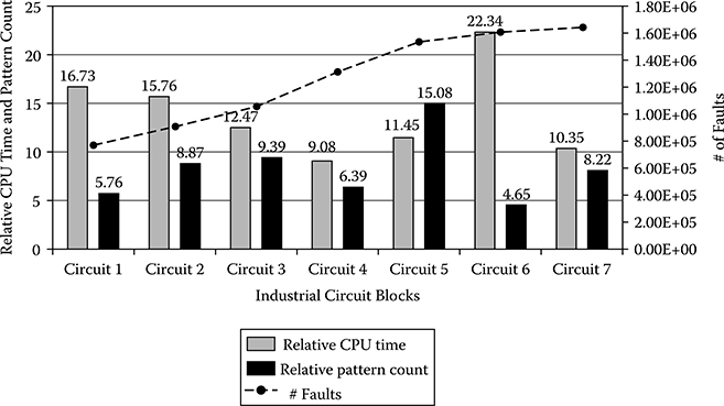
Figure 6.1
CPU run time and pattern count of timing-aware ATPG relative to traditional TDF ATPG for subblocks of an industrial microprocessor circuit.
Generate a list of timing-sensitive paths using an STA tool. Usually, the tool reports only the most critical paths (e.g., paths with less than 5% slack margin).
Next, feed the reported set of paths into an ATPG tool to generate patterns targeting these paths.
There are, however, several drawbacks to this flow. First, the predicted timing data rarely match the real delays observed on silicon [Cheng 2000] due to process variations. As a result, if we target only a small list of critical paths, we are likely to miss real critical delay paths due to timing variations and secondary effects such as cross talk. As reported [Zolotov 2010], all semiconductor companies recognize this problem. One solution is to report a larger group of paths by increasing the slack margin. For instance, one might report paths with 20% slack margin to account for delay variations. This approach, however, introduces another drawback of PDF ATPG flow: The number of paths increases exponentially as the slack margin is increased. Hence, increased slack margins are also impractical for large designs.
We experimented with production circuits to quantify this problem. We observed that, for various industrial designs, the number of paths reported for a 5% slack margin was more than 100,000. The ATPG tool generated twice the number of patterns compared with 1-detect TDF patterns, and it could test less than half of all PDFs. (All other paths remained untested.) Increasing the slack margin to 10% pushed the number of paths to millions and effectively made it infeasible to run the PDF ATPG. Results for slack margin limits as high as 20% are practically impossible to report due to disk space limitations. This highlights the problems of using PDF ATPG for large industrial circuits fabricated using nanoscale complementary metal oxide semiconductor (CMOS) processes that are subject to process variations and provide some quantitative data points.
Statistical static timing analysis (SSTA) can generate variability-aware delay data. Although a complete SSTA flow takes considerable computation time [Forzan 2007; Nitta 2007], simplified SSTA-based approaches could be used for pattern selection, as shown by some authors [Chao 2004; Lee 2005]. Chao and coworkers [Chao 2004] proposed an SSTA-based test pattern quality metric to detect SDDs. The computation of the metric required multiple dynamic timing analysis runs for each test pattern using randomly sampled delay data from Gaussian pin-to-pin delay distributions. The proposed metric was also used for pattern selection. Other authors [Lee 2005] focused on timing hazards and proposed a timing hazard-aware SSTA-based pattern selection technique.
The complexity of today’s ICs and shrinking process technologies also leads to prohibitively high test data volumes. For example, the test data volume for TDFs is two to five times higher than stuck-at faults [Keller 2004], and it has also been demonstrated that test patterns for such sequence- and timing-dependent faults are more important for newer technologies [Ferhani 2006]. The 2007 International Technology Roadmap for Semiconductors (ITRS) predicted that the test data volume for ICs will be as much as 38 times larger and the test application time will be about 17 times longer in 2015 than it was in 2007. Therefore, efficient generation, pattern grading, and selection methods are required to reduce the total pattern count while effectively targeting SDDs.
This chapter presents a statistical approach based on the concept of output deviations to select the most effective test patterns for SDD detection [Yilmaz 2008c, 2010]. The literature indicates that, for academic benchmark circuits, there is high correlation between the output deviations measure for test patterns and the sensitization of long paths under process variation. These benchmark circuits report significant reductions in CPU run time and pattern count and higher test quality compared with commercial timing-aware ATPG tools. We also examine the applicability or effectiveness of this approach for realistic industrial circuits. We present the adaptation of the output deviation metric to industrial circuits. This work enhanced the framework of output deviations to make it applicable for such circuits.
Experimental results showed the proposed method could select the highest-quality patterns effectively from test sets too large for use in their entirety in production test environments with tight pattern count limits. Unlike common industry ATPG practices, it also considers delay faults caused by process variations. The proposed approach incurs a negligible runtime penalty. For two important quality metrics—coverage of long paths and long-path coverage ramp up—this approach outperforms a commercial timing-aware ATPG tool for the same pattern count.
6.3 Probabilistic Delay Fault Model and Output Deviations for SDDs
This section reviews the concept of output deviations, then describes how we extended the deviation-based pattern selection method of earlier work to industrial circuits.
6.3.1 Method of Output Deviations
Yilmaz and coworkers [Yilmaz 2008c] introduced the concepts of gate delay defect probabilities (DDPs) and signal transition probabilities (STPs). These probabilities introduce the notion of confidence levels for pattern pairs.
In this section, we first review the concept of DDPs (Section 6.3.1.1) and STPs (Section 6.3.1.2). These probabilities extend the notion of confidence levels, defined by Wang et al. [Wang 2008a] for a single pattern, to pattern pairs. Next, we show how to use these probability values to propagate the effects of a test pattern to the test observation points (scan flip-flops/primary outputs) (Section 6.3.1.3). We describe the algorithm used for signal probability propagation (Section 6.3.1.4). Finally, we describe how to rank and select test patterns from a large repository (Section 6.3.1.5).
6.3.1.1 Gate Delay Defect Probabilities
This approach assigns DDPs to each gate in a design, providing DDPs for a gate in the form of a matrix called the delay defect probability matrix (DDPM). Table 6.1a shows the DDPM for a two-input OR gate. The rows in the matrix correspond to each input port of the gate, and the columns correspond to the initial input state during a transition.
Assume the inputs are shown in the order IN0, IN1. If there is an input transition from 10 to 00, the corresponding DDPM column is 10. Since IN0 causes the transition, the corresponding DDPM row is IN0. As a result, the DDP value corresponding to this event is 0.5, showing the probability that the corresponding output transition is delayed beyond a threshold.
Table 6.1
Example DDPM for a Two-Input OR Gate: (a) Traditional Style and (b) New Style
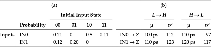
For initial state 11, both inputs should switch simultaneously to have an output transition. This approach merges corresponding DDPM entries due to this requirement. We chose the entries in Table 6.1 arbitrarily for the sake of illustration. The real DDPM entries are much smaller than those shown in this example.
For an N-input gate, the DDPM consists of N * 2N entries, each holding one probability value. If the gate has more than one output, each output of the gate has a different DDPM. Note that the DDP is 0 if the corresponding event cannot provide an output transition. Consider DDPM(2,3) in Table 6.1. When the initial input state is 10, no change in IN1 might cause an output transition because the OR gate output is already at high state; even if IN1 switches to high (1), this will not cause an output transition.
We next discuss how to generate a DDPM. Each entry in a DDPM indicates the probability that the delay of a gate is more than a predetermined value (i.e., the critical delay value TCRT). Given the probability density function of a delay distribution, the DDP is calculated as the probability that the delay is higher than TCRT.
For instance, if we assume a Gaussian delay distribution for all gates (with mean μ) and set the critical delay value to μ + X, each DDP entry can be calculated by replacing TCRT with μ + X and using a Gaussian probability density function. Note that the delay for each input-to-output transition could have a different mean μ and standard deviation σ.
We can obtain the delay distribution in different ways: (1) using the delay information provided by an SSTA-generated SDF file; (2) using slow, nominal, and fast process corner transistor models; or (3) simulating process variations. In the third method, which we apply in this chapter to academic benchmarks, we first determined transistor parameters affecting the process variation and the limits of the process variation (3σ). Next, we ran Monte Carlo simulations for each library gate under different capacitive loading and input slew rate conditions. Once this process finds distributions for the library gates, depending on the layout, it can update the delay distributions for each individual gate. Once this process obtains distributions, it can set TCRT appropriately to compute the DDPM entries. We can simulate the effects of cross talk separately, updating the delay distributions of individual gates/wires accordingly.
The generation of the DDPMs is not the main focus of this chapter. We consider DDPMs analogous to timing libraries. Our goal is not to develop the most effective techniques for constructing DDPMs; rather, we are using such statistical data to compute deviations and use them for pattern grading and pattern selection. In a standard industrial flow, specialized timing groups develop statistical timing data, so the generation of DDPMs is a preprocessing step and an input to the ATPG-focused test automation flow.
We have seen that small changes in the DDPM entries (e.g., less than 15%) have a negligible impact on the pattern selection results. We attribute this finding to the fact that any DDPM changes affect multiple paths in the circuits, thus amortizing their impact across the circuit and the test set. The absolute values of the output deviations are less important than the relative values for different test patterns.
6.3.1.2 Propagation of Signal Transition Probabilities
Since pattern pairs are required to detect TDFs, there might be a transition on each net of the circuit for every pattern pair. If we assume there are only two possible logic values for a net (i.e., LOW [L] and HIGH [H]), the possible signal transitions are L → L, L → H, H → L, and H → H. Each of these transitions has a corresponding probability, denoted by PL→L, PL→H, PH→L, and PH→H, respectively, in a vector form (<…>): < PL→L, PL→H, PH→L, PH→H >. We refer to this vector as the STP vector. Note that L → L or H → H implies that the net keeps its value (i.e., no transition occurs).
The nets directly connected to the test application points are called initialization nets (INs). These nets have one of the STPs, corresponding to the applied transition test pattern, equal to 1. All the other STPs for INs are set to 0. When signals propagate through several levels of gates, this approach can compute STPs using the DDPM of the gates. Note that interconnects can also have DDPMs to account for cross talk. In this chapter, due to the lack of layout information, we only focus on variations’ impact on gate delay. The overall deviation-based framework is, however, general, and it could easily accommodate interconnect delay variations if layout information is available, as reported by Yilmaz et al. [Yilmaz 2008b].
Definition 1
Let PE be the probability that a net has the expected signal transition. The deviation on that net is defined by Δ = 1 – PE. We apply the following rules during the propagation of STPs:
If there is no output signal transition (output keeps its logic value), then the deviation on the output net is 0.
If there are multiple inputs that might cause the expected signal transition at the output of a gate, only the input-to-output path that causes the highest deviation at the output net is considered. The other inputs are treated as if they have no effect on the deviation calculation (i.e., they are held at the noncontrolling value).
When multiple inputs must change at the same time to provide the expected output transition, we consider all required input-to-output paths of the gate. We discard only the unnecessary (redundant) paths.
A key premise of this chapter is that we can use output deviations to compare path lengths. As in the case of path delays, the net deviations also increase as the signal propagates through a sensitized path, a property that follows from the rules used to calculate STPs for a gate output. Next, we formally prove this claim.
Lemma 1
For any net, let the STP vector be given by < PL→L, PL→H, PH→L, PH→H >. Among these four probabilities (i.e., < PL→L, PL→H, PH→L, PH→H >), at least one is nonzero, and at most two can be nonzero.
PROOF
If there is no signal value change (the event L→L or H→H), the expected STP is 1, and all other probabilities are 0. If there is a signal value change, only the expected signal transition events and the delay fault case have nonzero probabilities associated with them. The delay fault case for an expected signal value change of L → H is L → L (the signal value does not change because of a delay fault). Similarly, the delay fault case for an expected signal value change of H → L is H → H.
Theorem 1
The deviation on a net always increases or stays constant on a sensitized path if the signal probability propagation rules are applied.
PROOF
Consider a gate with K inputs and one output. The signal transition on the output net depends on one of the following cases: From Lemma 1, we need to consider only two cases:
Only one of the input port signal transitions is enough to create the output signal transition.
Multiple input port signal transitions are required to create the output signal transition.
Let POUT,j be the probability that the gate output makes the expected signal transition for a given pair of patterns on input j, where 1 ≤ j ≤ K. Let ΔOUT,j = 1 – POUT,j be the deviation for the net corresponding to the gate output.
Case (i)
Consider a signal transition on input j. Let Qj be the probability of occurrence of this transition. Let dj be the entry in the gate’s DDPM that corresponds to the given signal transition on j. The probability that the output makes a signal transition is
We assume an error at a gate input is independent of the error introduced by the gate. Note POUT,j ≤ Qj since 0 ≤ dj ≤ 1. Therefore, the probability of getting the expected signal transition decreases, and the deviation ΔOUT,j = 1 – POUT,j increases (or does not change) as we pass through a gate on a sensitized path. The overall output deviation on the output net is
Case (ii)
Suppose L input ports (L > 1), indexed 1, 2, …, L, are required to make a transition for the gate output to change. Let . The output deviation for the gate in this case is
Note that , 1 ≤ i ≤ L since . Therefore, we conclude that the probability of getting the expected transition on a net either decreases or remains the same as we pass through a logic gate. In other words, the deviation is monotonically nondecreasing along a sensitized path.
Example
Figure 6.2 shows STPs and their propagation for a simple circuit. The dark boxes show test stimuli and the expected fault-free transitions on each net. The angled brackets (< … >) show calculated STPs. Tables 6.1 and 6.2 give the DDPMs of the gates (OR, AND, XOR, and INV) used in this circuit. The entries in both tables are arbitrary. We calculated the deviations in the following example based on the rules previously mentioned for the example circuit in Figure 6.2:
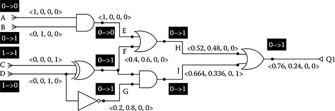
Figure 6.2 Example of the propagation of STPs through the gates of a logic circuit.
Table 6.2
Example DDPM for AND, XOR, INV

- Net E: There is no output change, which implies that E has the STP <1,0,0,0>.
- Net F: The output changes due to IN1 (net D) of XOR. There is a DDP of 0.4. It implies that, with a probability of 0.4, the output will stay at LOW value (i.e., the STP for net F is <0.4,0.6,0,0>).
- Net G: Output changes due to IN0 (net D) of INV (i.e., the STP for net G is <0.2,0.8,0,0>).
- Net H: Output changes due to IN1 (net F) of OR.
- If IN1 stays at LOW, output does not change. Therefore, the STP for net H is0.4 • <1,0,0,0>, where • denotes the dot product;
- If IN1 goes to HIGH, output changes with a DDP of 0.2 (i.e., the STP for net H is 0.6 • <0.2,0.8,0,0>);
- Combining all the preceding cases, the STP for net H is <0.52,0.48,0,0>.
- Net J: Output changes due to both IN0 (net F) and IN1 (net G) of AND (both required).
- If both stay at LOW, output does not change, which implies the STP for net J is 0.4 • 0.2 • <1,0,0,0>;
- If one stays at LOW, output does not change (i.e., the STP for net J is 0.4 • 0.8 • <1,0,0,0> + 0.6 • 0.2 • <1,0,0,0>);
- If both go to HIGH, the output changes with a DDP. Since both inputs change, we use the maximum DDP (i.e., the STP for net J is 0.6 • 0.8 • <0.3,0.7,0,0>);
- Combining all the preceding cases, the STP for net J is <0.664,0.336,0,0>.
- Net Q1: The output changes due to only one of the inputs of OR. We need to calculate the deviation for both cases and select the one that causes maximum deviation at the output (Q1).
- For IN0 (net H) of OR:
- − If IN0 stays at LOW, the output does not change (i.e., the STP for net Q1 is 0.52 • <1,0,0,0>);
- − If IN0 goes to HIGH, the output changes with a DDP (i.e., the STP for net Q1 is 0.48 • <0.5,0.5,0,0>);
- − Combining all the preceding cases, the STP for net Q1 is <0.76,0.24,0,0>.
- For IN1 (net J) of OR:
- − If IN1 stays at LOW, the output does not change (i.e., the STP for net Q1 is 0.664 • <1,0,0,0>);
- − If IN1 goes to HIGH, the output changes with a DDP (i.e., the STP for net Q1 is 0.336 • <0.2,0.8,0,0>);
- − Combining all the preceding cases, the STP for net Q1 is <0.7312,0.2688,0,0>.
- Since IN0 provided the higher deviation, we finally conclude that the STP for net Q1 is <0.76,0.24,0,0>.
Hence, the deviation on Q1 is 0.76.
6.3.1.3 Implementation of Algorithm for Propagating Signal Transition Probabilities
We use a depth-first procedure to compute STPs for large circuits. A depth-first algorithm processes only the nets required to find the output deviation on a specific observation point. In this way, less gate pointer stacking is required relative to simulating the deviations starting from INs and tracing forward.
We first assign STPs to all INs. Then, we start from the observation points (outputs) and backtrace until we find a processed net (PN). A PN has all the STPs assigned. Figure 6.3 gives the pseudocode for the algorithm.
If the number of test patterns is Ns and the number of nets in the circuit is Nn, the worst-case time complexity of the algorithm is O(NsNn). However, we could easily make the algorithm multithreaded because the calculation for each pattern is independent of other patterns (we assume full-scan designs in this chapter). In this case, if the number of threads is T, the complexity of the algorithm is reduced to O((NsNn)/T).

Figure 6.3
Signal transition probability propagation algorithm for calculating output deviations.
6.3.1.4 Pattern-Selection Method
In this section, we describe how to use output deviations to select high-quality patterns from an n-detect transition fault pattern set. The number of test patterns to select is a user input (e.g., S). The user can set the parameter S to the number of 1-detect timing-unaware patterns, the number of timing-aware patterns, or any other value that fits the user’s test budget.
In our pattern selection method, we target topological coverage as well as long-path coverage. As a result, we attempt to select patterns that sensitize a wide range of distinct long paths. In this process, we also discard low-quality patterns to find a small set of high-quality patterns.
For each test observation point POj, we keep a list of Np most effective patterns in EFFj (Figure 6.4, lines 1–3). The patterns in EFFj are the best unique-pattern candidates for exciting a long path through POj. During deviation computation, no pattern ti is added to EFFj if the output deviation at POj is smaller than a limit ratio DLIMIT of the maximum instantaneous output deviation (Figure 6.4, line 10). We can use DLIMIT to discard low-quality patterns. If the output deviation is larger than this limit, we first check whether we have added a pattern to EFFj with the same deviation (Figure 6.4, line 11). It is unlikely that two different patterns will create the same output deviation on the same output POj while exciting different nonredundant paths. Since we want higher topological path coverage, we skip these cases (Figure 6.4, line 11). Although this assumption might not necessarily be true, we assume for the sake of completeness that it holds for most cases.
If we observed a unique deviation on POj, we first check whether EFFj is full (whether it already includes Np patterns; see Figure 6.4, line 12). Pattern ti is added to EFFj along with its deviation if EFFj is not full or if ti has a greater deviation than the minimum deviation stored in EFFj (Figure 6.4, lines 12–17). We measure the effectiveness of a pattern by the number of occurrences of this pattern in EFFj for all values of j. For instance, if—at the end of deviation computation—pattern A was included in the EFF list for 10 observation points and pattern B was listed in the EFF list for 8 observation points, we conclude that pattern A is more effective than pattern B.

Figure 6.4
Deviation computation algorithm for pattern selection.
Once the deviation computation is completed, this approach generates the list of pattern effectiveness and carries out the final pattern filtering and selection (Figure 6.5). First, pattern effectiveness is generated (Figure 6.5, lines 1–9). Since Max_Dev updates on the fly, we could miss some low-quality patterns. As a result, we need to filter by Max_Dev (DLIMIT) again to discard low-quality patterns from the final pattern list (Figure 6.5, line 5). Setting DLIMIT to a high value might result in discarding most of the patterns, leaving only the best few patterns. Depending on DLIMIT, the number of remaining patterns might be less than S.
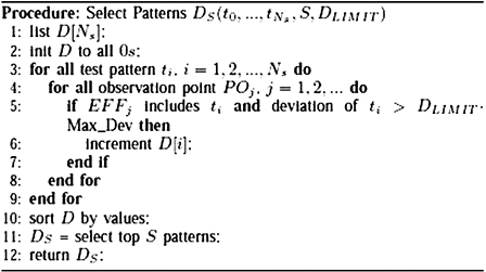
Figure 6.5
Pattern selection algorithm.
In the next stage, this approach re-sorts the patterns by their effectiveness (Figure 6.5, line 10). Finally, until the selected pattern number reaches S or this approach selects all patterns, the top patterns are selected (Figure 6.5, line 11). The computational complexity of the selection algorithm is O(Nsp), where Ns is the number of test patterns, and p is the number of observation points. This procedure is very fast since it only includes two nested for loops and a simple list item existence check.
6.3.2 Practical Aspects and Adaptation to Industrial Circuits
We need to revisit the input data required to compute output deviations to ensure provision of appropriate information, and we can use the proposed approach with the data available in an industrial project.
The two most significant inputs required by the previously proposed output deviations method are the gate and interconnect delay variations and TCRT for gates and interconnects. Typically, a timing group computes delay variations for library gates based on design-for-manufacturability (DfM) rules. The available data are the input-to-output delay values for worst, nominal, and best conditions. Delay variations for interconnects are computed based on DfM rules defining the range of resistance and capacitance variations for different metal layers and vias.
The main challenge in practice is finding a specific TCRT for gates and interconnects. Defining a TCRT for individual gates and interconnects is not feasible for industrial circuits because allowed delay ranges are defined at the circuit or subcircuit levels. Due to this limitation, it was not possible to generate DDPM tables for gates and interconnects. As a result, we redefined the manner in which this approach computed output deviations.
We first assumed independent Gaussian delay distributions for each path segment (i.e., gates and interconnects), where nominal delay was used as the mean, and the worst-case delay was used as $3sigma$. Instead of using specific probability values in DDPMs, we used mean delay and variances for each gate instance and interconnect. An example of the new DDPM (with entries chosen arbitrarily) for a two-input OR gate is shown in Table 6.1b. The rows in the matrix correspond to each input-to-output timing arc, and the columns correspond to the mean μ and variance σ2 of the corresponding L → H (rising) or H → L (falling) output transition.
Similarly, instead of propagating the STPs, we propagated the mean delay and variance on each path using the central limit theorem (CLT) [Trivedi, 2001], similar to the method proposed by Park et al. [Park 1989].
Since we assumed independent Gaussian distributions, we can use the following equations to calculate the mean value and standard deviation of the path probability density function [Trivedi 2001].
where μi and σi are the probability density function mean value and standard deviation of segment i, respectively; μc and σc are the path probability density function mean value and standard deviation, respectively; and N is the number of path segments.
Even if we do not assume Gaussian distributions for each delay segment, as long as segment delays are independent distributions with finite variances, the CLT ensures that the path delay—which is the sum of segment delays—converges to a Gaussian distribution [Trivedi 2001].
We defined TCRT for the circuit as a fraction of the functional clock period Tfunc of the circuit. In our experiments, we used the values 0.7 * Tfunc, 0.8 * Tfunc, 0.9 * Tfunc, and Tfunc. For each case, the output deviation is the probability that the calculated delay on an observation point (scan flip-flops or primary outputs) is larger than TCRT.
We also adapted the pattern selection method by introducing a degree of path enumeration to the pattern selection procedure. We implemented this change to ensure selection of all patterns exciting the delay-sensitive paths. We developed an in-house tool to list all the sensitized paths for a TDF pattern, in addition to each segment of the sensitized paths. This tool enumerates all paths sensitized by a given test pattern. The steps in this flow are as follows:
Use commercial tools for ATPG and fault simulation.
For each pattern, the ATPG tool reports the detected TDFs. This report includes the net name as well as the type of signal transition (i.e., falling or rising).
Our in-house tool finds the active nets (i.e., nets that have a signal transition on them) in the circuit under test. This step has O(log N) worst-case time complexity.
Starting from scan flip-flops and primary inputs, trace forward each net with a detected fault. Note that, if a fault is detected, it means this net reaches a scan flip-flop through other nets with detected faults. If the sensitized path has no branching on it, the complexity of this step is O(N). However, if there are K branches on the sensitized net, and if all these branches create a different sensitized path, the complexity of this step is O(NK).
Note that, although unlikely, if a test pattern could test all nets at the same time, the run time of the sensitized path search procedure would be very high. However, our simulations on academic benchmarks and industrial circuits showed that, for most cases, a single test pattern can test a maximum of 5–10% of the nets for transition faults, and the sensitized paths (except clock logic cones) had a small amount of branching. Our analysis showed that the number of fan-out pins was three or fewer for 95% of all instances. Although we found some cases in which the number of fan-outs was high, the majority of them were on clock logic cones. In our sensitized path analysis, we excluded clock cones. As a result, the run time of the sensitized path search procedure was considerably shorter than the ATPG run time.
Our simulations showed that for the given AMD circuit blocks, there were no sensitized paths longer than Tfunc. As a result, setting TCRT to Tfunc led to selection of no patterns. Thus, we do not present results for TCRT = Tfunc.
To minimize total run time, we integrated the deviation computation procedure into our sensitized path search tool, which we named Pathfinder. As a result, Pathfinder computes the output deviations and finds all sensitized paths at the same time. In the next step, it assigns all sensitized paths a weight equal to the output deviation of their endpoints. We define the weight of a test pattern as the sum of the weights of all the paths sensitized by this pattern.
The weights of test patterns drive pattern selection. This approach selects patterns with the greatest weights first. However, it is possible that some of the sensitized paths of two different patterns are the same. If the selected patterns have already detected a path, it is not necessary to use it for evaluating the remaining patterns. The objective of this method is to minimize the number of selected patterns while still sensitizing most delay-sensitive paths.
The proposed pattern selection procedure orders the largest weighted pattern first. After selecting this pattern, we recalculate the weight of all the remaining patterns by excluding paths detected by the selected pattern. Then, this approach selects the pattern with the greatest weight in the remaining pattern set and repeats this procedure until it meets some stopping criterion (e.g., the number of selected patterns or the minimum allowed pattern weight). Since this approach sorts the selected patterns based on effectiveness, there is no need to re-sort the final set of patterns.
The final stage of the proposed method is to run top-off TDF ATPG to recover TDF coverage. In all cases, top-off ATPG generated much fewer patterns than the 1-detect TDF pattern count. Since the main purpose of this chapter is to show the application of pattern selection on industrial circuits, we do not present results for this step.
6.3.3 Comparison to SSTA-Based Techniques
The proposed method is comparable to SSTA-based techniques (e.g., [Chao 2004], [Lee 2005]). Table 6.3 illustrates the summary of this comparison, including both the original method of output deviations and the new method. Both the work of Chao et al. [Chao 2004] and the proposed work present a transition test pattern quality metric for the detection of SDDs in the presence of process variations. The focus of the work of Lee et al. [Lee 2005], on the other hand, was to present a timing hazard-aware SSTA-based technique for the same target defect group. The work of Chao et al. [Chao 2004] and the proposed work do not cover timing hazards. The formulation is different in these methods. Chao and coworkers [Chao 2004] run dynamic timing analysis multiple times for each test pattern to create a delay distribution, using simple operators (e.g., +/-) while propagating the delay values. Lee et al. [Lee 2005] run statistical dynamic timing analysis once for each test pattern, using simple operators for delay propagation (similar to [Chao 2004]), but the analysis of timing hazards adds complexity to their formulation. Both of these methods assume a Gaussian delay distribution.
On the other hand, in the original proposed work, there was no assumption regarding the shape of the delay distribution. This is because we use probability values instead of distributions. We compute the metric using probability propagation. The drawback of the original proposed method is that its effectiveness drops if the combinational depth of the circuit is very large (i.e., greater than 10). The new proposed method overcomes this limitation. Similarly, both previous studies [Chao 2004; Lee 2005] and the new proposed method can handle large combinational depths; using CLT, it could be argued that their accuracy might increase with the increased combinational depth. We expect the run time of SSTA-based WHAT [Chao 2004; Lee 2005] to limit its applicability to industrial-size designs. Further optimization might eliminate this shortcoming. On the other hand, the proposed method is quick, and its run time increases less rapidly with increase in circuit size. Since the new proposed method uses a path enumeration procedure, the run time could be a limiting factor if the number of sensitized paths is very large. However, our simulations showed that this limitation was not observed on the tested circuit blocks.
6.4 Simulation Results
In this section, we present experimental results obtained for four industrial circuit blocks. We provide details for the designs and the experimental setup in Section 6.4.1, then present simulation results in Sections 6.4.2 and 6.4.3.
Table 6.3
Comparison of SSTA-Based Approaches
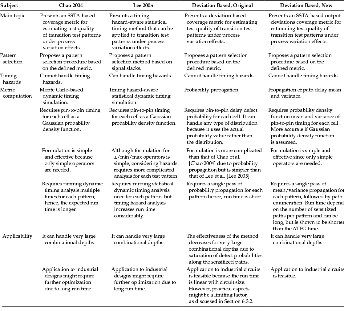
Table 6.4
Description of the Circuit Blocks
Benchmark |
Functionality |
Circuit A |
Cache block |
Circuit B |
Execution unit |
Circuit C |
Execution unit |
Circuit D |
Load-store unit |
6.4.1 Experimental Setup and Benchmarks
We performed all experiments on a pool of state-of-the-art servers running Linux with at least four processors available at all times and 16 GB of memory. We used Pathfinder to compute output deviations and find sensitized paths and implemented select patterns using C++. We used a commercial ATPG tool to generate $n$-detect TDF test patterns and timing-aware TDF patterns for these circuits. We forced the ATPG tool to generate launch-off-capture (LOC) transition fault patterns. We prevented the primary input change during capture cycles and the observation of primary outputs to simulate realistic test environments. We performed all ATPG runs and other simulations in parallel on four processors.
We selected blocks from functional units of state-of-the-art AMD microprocessor designs. Each block has a different functionality. Table 6.4 shows the functionality of each block.
While generating n-detect (n = 5 and n = 8) TDF patterns, we placed no limits on the number of patterns generated and set no target for fault coverage. We allowed the tool to run in automatic optimization mode. In this mode, the ATPG tool sets compaction and ATPG efforts, determines ATPG abort limits, and controls similar user-controlled options. While generating timing-aware ATPG patterns, we used two different optimization modes. In ta-1 mode, we forced the tool to sensitize the longest paths to obtain the highest-quality test patterns, at the expense of increased CPU run time and pattern count. In ta-2 mode, we relaxed the optimization criteria to decrease run time and pattern count penalty.
We obtained timing information for gate instances from a timing library, as described in Section 6.3.2. Both the ATPG and Pathfinder tools used the same timing data. The ATPG tool used nominal delay values because it was not designed to use delay variations. We did not model interconnect delays, leaving that for future work. We allowed the pattern selection in Pathfinder to continue until it selected all nonzero weight patterns.
6.4.2 Simulation Results
We grouped the simulations for generating patterns into three main categories:
n-detect TDF ATPG: We generated patterns for a range of multiple-detect values. We used n = 1, 3, 5, and 8. The results for n = 5 and n = 8 are shown in this section. We used the n-detect TDF pattern set because we needed a pattern repository that was likely to sensitize many long paths, comparable to the number of long paths sensitized by timing-aware ATPG. Using a large number of patterns and n-detect TDF ATPG satisfied this requirement.
Timing-aware ATPG using different optimization modes: We generated timing-aware patterns for optimization modes ta-1 and ta-2, as described previously.
Selected patterns: We used our in-house Pathfinder tool to select high-quality patterns from both n-detect and timing-aware pattern sets.

Figure 6.6
Normalized number of test patterns for n-detect ATPG, timing-aware ATPG (ta-1 and ta-2), and the proposed pattern selection method (dev). TCRT was set to 0.8 * Tfunc and 0.9 * Tfunc for the proposed method. All values were normalized by the result for n = 1.
We observed the pattern count for timing-aware ATPG was much greater than the TDF ATPG pattern count. As n increased, the number of patterns in the n-detect pattern set also increased. Figure 6.6 shows the number of test patterns generated by n-detect ATPG and timing-aware ATPG and the number of patterns selected by the proposed method (while retaining the long-path coverage provided by the much larger test set). Figure 6.6 shows results for TCRT = 0.8 * Tfunc and TCRT = 0.9 * Tfunc. We find that, for all cases, the number of patterns selected by the proposed method was only a very small fraction of the overall pattern set. When TCRT = 0.8 * Tfunc, the proposed scheme selected only 7% of the available patterns for circuit A from the timing-aware pattern set ta-1. We obtained similar results for other benchmarks. As expected, as TCRT increased, the number of selected patterns dropped as low as 3% of the original pattern set.

Figure 6.7
Normalized CPU time usage for n-detect ATPG, timing-aware ATPG (ta-1 and ta-2), and the proposed pattern-grading and pattern selection method (dev). TCRT was set to 0.8 * Tfunc for the proposed method. All values were normalized by the result for n = 1.
The results for CPU runtime usage were as striking as the pattern count results. Figure 6.7 shows the normalized CPU runtime usage results for n-detect ATPG, timing-aware ATPG (ta-1 and ta-2), and the proposed pattern grading and pattern selection method (dev). As seen, the complete processing time (pattern grading and pattern selection) for the proposed scheme was only a fraction of the ATPG run time. For instance, for circuit C, n = 8, ATPG run time was 10 times longer than the pattern grading and selection time. For circuit B, the time spent for pattern grading and selection was only 2.5% of the ta-1 timing-aware ATPG run time. Note that the CPU run time of the proposed method depended on the applied TCRT. Very low TCRT values could increase the run time because the number of paths discarded on the fly will be lower.
Since the proposed scheme allowed us to select as many patterns as needed to cover all high-risk paths, the patterns selected by the proposed scheme sensitized all of the long paths that can be excited by the given base pattern set using only a fraction of the test patterns. Note that the effectiveness of the base pattern set bound the effectiveness of our method.
The long-path coverage ramp up for the selected patterns was also significantly better than both n-detect and timing-aware ATPG patterns. Figure 6.8 presents the results for the long-path coverage ramp up with respect to the number of applied patterns. For all cases, the selected and sorted patterns covered the same number of long paths much faster and used far fewer patterns.

Figure 6.8
The long-path coverage ramp up using the base 8-detect TDF ATPG (n = 8), timing-aware ATPG in modes ta-1 and ta-2, selected patterns from 8-detect TDF ATPG [n = 8 (dev)] and timing-aware ATPG [ta-1 (dev), ta-2 (dev)]. TCRT was 0.8 * Tfunc for the proposed method: (a) circuit A, (b) circuit B, and (c) circuit C.
6.4.3 Comparison of the Original Method to the Modified Method
In this section, we compare the original deviation-based method [Yilmaz 2008c] to the new method proposed. We used three ASIC-like IWLS benchmark circuits for this comparison. Note that, although the Register Transfer Level (RTL) codes of these benchmarks were the same as the ones used by Yilmaz and coworkers [Yilmaz 2008c], the synthesized net lists were different due to library and optimization differences. To make a fair comparison, we reimplemented the original method [Yilmaz 2008c] to use the same pattern selection method proposed in this chapter. The only difference between those methods was this new procedure to calculate metrics. We ran all simulations on servers with similar configurations.
Figure 6.9 shows a comparison of CPU run time between the original and the modified method. As seen, for all cases, the new method had a superior CPU run time compared with the original method. The main reason for the difference between CPU run times is that the original method consumed more time to evaluate patterns due to the larger number of selected patterns. Depending on the benchmark, the impact of this effect on the overall CPU run time might be considerable, as in the case of aes_core, or it might be negligible, as in the case of systemcaes.
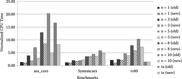
Figure 6.9
Normalized CPU run time for the selected n-detect ATPG and timing-aware ATPG patterns for the original method (old) and the modified method (new). All values were normalized by the result for n = 1 (new).
Figure 6.10 presents the normalized number of sensitized long paths for the original and the modified methods. Although the modified method consistently sensitized more long paths than the original method, the difference was rather small. We can better analyze Figure 6.10 if we consider Figure 6.11. Figure 6.11 shows the normalized number of selected patterns for each method. As seen, the modified method consistently selected fewer patterns than the original method. The difference was significant for benchmarks systemcaes and tv80. Although the number of sensitized long paths was similar for these methods, the number of selected patterns was significantly different. This result shows that the modified method was more efficient than the original method in selecting high-quality patterns. The main reason for the difference in the number of selected patterns was that, due to deviation saturation on long paths, the original method was unable to distinguish between long paths and shorter paths. As a result, the original method selected more patterns to cover all of these paths.

Figure 6.10
Normalized number of sensitized long paths for the selected n-detect ATPG and timing-aware ATPG patterns for the original method (old) and the modified method (new). All values were normalized by the result for n = 1 (new).
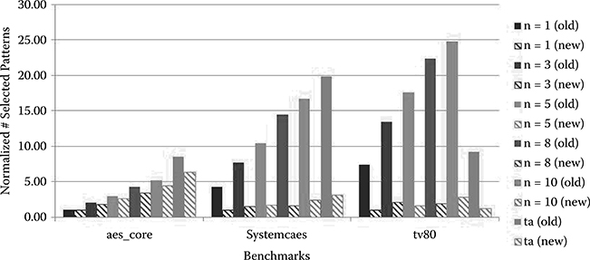
Figure 6.11
Normalized number of selected patterns from the base n-detect ATPG and timing-aware ATPG patterns for the original method (old) and the modified method (new). All values were normalized by the result for n = 1 (new).
6.5 Conclusions
We have presented a test-grading technique based on output deviations for SDDs and applied it to industrial circuits. We have redefined the concept of output deviations to apply it to industrial circuit blocks and have shown we can use it as an efficient surrogate metric to model the effectiveness of TDF patterns for SDDs. Experimental results for the industrial circuits showed the proposed method intelligently selected the best set of patterns for SDD detection from an n-detect or timing-aware TDF pattern set, and it excited the same number of long paths compared with a commercial timing-aware ATPG tool using only a fraction of the test patterns and with negligible CPU runtime overhead.
6.6 Acknowledgments
Thanks are offered to Prof. Krishnendu Chakrabarty of Duke University and Prof. Mohammad Tehranipoor and Ke Peng of the University of Connecticut for their contributions to this chapter. Colleagues at AMD are thanked for valuable discussions.
References
[Ahmed 2006b] N. Ahmed, M. Tehranipoor, and V. Jayram, Timing-based delay test for screening small delay defects, in Proceedings IEEE Design Automation Conference, 2006.
[Chao 2004] C.T.M. Chao, L.C. Wang, and K.T. Cheng, Pattern selection for testing of deep sub-micron timing defects, in Proceedings IEEE Design Automation and Test in Europe, 2004, vol. 2, pp. 1060–1065.
[Cheng 2000] K.T. Cheng, S. Dey, M. Rodgers, and K. Roy, Test challenges for deep sub-micron technologies, in Proceedings IEEE Design Automation Conference, 2000, pp. 142–149.
[Ferhani 2006] F.F. Ferhani and E. McCluskey, Classifying bad chips and ordering test sets, in Proceedings IEEE International Test Conference, 2006.
[Forzan 2007] C. Forzan and D. Pandini, Why we need statistical static timing analysis, in Proceedings IEEE International Conference on Computer Design, 2007, pp. 91–96.
[Keller 2004] B. Keller, M. Tegethoff, T. Bartenstein, and V. Chickermane, An economic analysis and ROI model for nanometer test, in Proceedings IEEE International Test Conference, 2004, pp. 518–524.
[Lee 2005] B.N. Lee, L.C. Wang, and M. Abadir, Reducing pattern delay variations for screening frequency dependent defects, in Proceedings IEEE VLSI Test Symposium, 2005, pp. 153–160.
[Nitta 2007] I. Nitta, S. Toshiyuki, and H. Katsumi, Statistical static timing analysis technology, Journal of Fujitsu Science and Technology 43(4), pp. 516–523, October 2007.
[Padmanaban 2004] S. Padmanaban and S. Tragoudas, A critical path selection method for delay testing, in Proceedings IEEE International Test Conference, 2004, pp. 232–241.
[Park 1989] E.S. Park, M.R. Mercer, and T.W. Williams, A statistical model for delay-fault testing, IEEE Design and Test of Computers 6(1), pp. 45–55, 1989.
[Trivedi 2001] K. Trivedi, Probability and Statistics with Reliability, Queuing, and Computer Science Applications, 2nd edition, Wiley, New York, 2001.
[Waicukauski 1987] J.A. Waicukauski, E. Lindbloom, B.K. Rosen, and V.S. Iyengar, Transition fault simulation, IEEE Design and Test of Computer 4(2), pp. 32–38, April 1987.
[Wang 2008a] Z. Wang and K. Chakrabarty, Test-quality/cost optimization using output-deviation-based reordering of test patterns, IEEE Transactions on Computer-Aided Design of Integrated Circuits and Systems 27, pp. 352–365, February 2008.
[Yilmaz 2008b] M. Yilmaz, K. Chakrabarty, and M. Tehranipoor, Interconnect-aware and layout-oriented test-pattern selection for small-delay defects, in Proceedings International Test Conference [ITC’08], 2008.
[Yilmaz 2008c] M. Yilmaz, K. Chakrabarty, and M. Tehranipoor, Test-pattern grading and pattern selection for small-delay defects, in Proceedings IEEE VLSI Test Symposium, 2008, pp. 233–239.
[Yilmaz 2010] M. Yilmaz, K. Chakrabarty, and M. Tehranipoor, Test-pattern selection for screening small-delay defects in very-deep sub-micrometer integrated circuits, IEEE Transactions on Computer-Aided Design of Integrated Circuits and Systems 29(5), pp. 760–773, 2010.
[Zolotov 2010] V. Zolotov, J. Xiong, H. Fatemi, and C. Visweswariah, Statistical path selection for at-speed test, IEEE Transactions on Computer-Aided Design of Integrated Circuits and Systems 29(5), pp. 749–759, May 2010.