
CHAPTER FOUR
Coding Style: Best-Known Method for Synthesis
Coding style plays a very important role for an ASIC design flow. “Bad” HDL (either Verilog or VHDL) code does not allow efficient optimization during synthesis. Logic that is generated from synthesis tools depends highly on the code that is written. A badly formed code would generally create bad logic. As the saying goes, “garbage in, garbage out.”
There are certain general guidelines to follow when it comes to coding style. By following these guidelines, a constant, good coding style can be attained. By having a good coding style, synthesis results are optimal.
4.1 NAMING CONVENTION
For a design project, a good naming convention is necessary. Naming convention is normally the most overlooked guideline when coding in HDL. Having a well-defined naming convention does not seem to sound important, but not having one can cause a lot of problems in the later stages of design, especially during the fullchip integration. It would be difficult for the designer to connect all the signals between modules of a fullchip if the signal names do not match.
By defining a naming convention, a set of rules is applied when the designer names the ports of a module. If each module in fullchip is based on the same set of naming rules, then it becomes much easier to connect these signals together in the fullchip level.
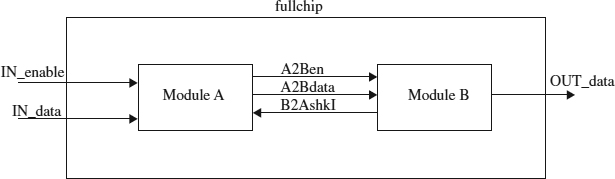
FIGURE 4.1. Diagram showing two submodules connected on a fullchip level.
Figure 4.1 is a diagram showing the fullchip level consisting of two modules, Module A and Module B. For this fullchip, let's assume the following rules for naming convention:
- The first three characters of the signal name must be capitalized.
- The first character must represent the name of the module on which the signal is an output from.
- The third character must represent the name of the module on which the signal is an input to.
- The second character must be the number 2.
- The fourth character and beyond for a signal name is the signal name. It must be in lowercase letters.
- Signals that propagate to the output at the fullchip level must have the first four characters “OUT_”. The signal's name after the first four characters is in lowercase letters.
- Signals that propagate from the input of the fullchip to a module must have the first three characters “IN_”. The signal's name after the first three characters is in lowercase letters.
- Any signal that is active low must end with the letter “I”. The character must be in uppercase.
Based on these naming rules, the names of the signals “IN_enable,” “IN_data,” and “OUT_data” are input and output signals at the fullchip level. The names of signals that are interconnects between Module A and Module B are “A2Ben,” “A2Bdata,” and “B2AshkI.”
The naming rules used here are just an example. A real design project may use naming rules that are similar to those shown here or they may be different.
Example 4.1 shows the Verilog code for Module A, Module B, and fullchip interconnect of both these modules.
Example 4.1 Verilog Example of Module A, Module B, and Fullchip Interconnect
module module_A (IN_enable, IN_data, B2AshkI, A2Ben, A2Bdata);
input IN_enable, IN_data, B2AshkI;
output A2Ben, A2Bdata;
// your Verilog code for module_A
endmodule

module module_B (A2Ben, A2Bdata, B2AshkI, OUT_data);
input A2Ben, A2Bdata;
output B2AshkI, OUT_data;
// your Verilog code for module_B
endmodule

module fullchip (IN_enable, IN_data, OUT_data);
input IN_enable, IN_data;
output OUT_data;
wire A2Ben, A2Bdata, B2AshkI;
module_A module_A_instance (IN_enable, IN_data, B2AshkI, A2Ben, A2Bdata);
module_B module_B_instance (A2Ben, A2Bdata, B2AshkI,
OUT_data);
endmodule
4.2 DESIGN PARTITIONING
It is good practice for the designer to partition a design into different modules. Each module should be partitioned with its own set of functionality or features. By having a good partitioning, the designer is able to break a complex design into smaller modules, thus giving more manageability to those modules. By following this method, the designer is able to localize the functionality of each module and write the HDL code for each module individually.
However, the designer needs to be careful when partitioning a design. Each module cannot be too small or too large. Partitioning modules that are too small will not be able to yield good synthesis optimization. Modules that are too large are difficult to be coded as well as synthesized to obtain optimal synthesis results. An acceptable module size that is manageable and allows good synthesis optimization, from a coding standpoint, would be around 5,000 to 15,000 gates.
Another point to keep in mind during design partitioning is the creation of additional interblock signaling. By partitioning into many blocks, a situation may occur whereby a need arises to create more signals for interfacing between these blocks. These additional signals may cause congestion in the layout phase as too many routing tracks are required. Therefore, it is important for the designer to fully understand the architecture and microarchitecture of a design before attempting to partition a design. Good partitioning brings advantages such as ease of manageability on each block. Bad partitioning brings disadvantages such as congestion on routing and increasing the die-size. Bad partitioning of a design also makes manageability of the design blocks a lot harder.
4.3 CLOCK
Most ASIC designs consist of at least one clock. Some may have more than one, some will only have one. Whether a design is a single clock design or multi-clock design, the designer needs to treat these clocks as global clocks. Global means that each clock is routed across all modules in the design, with the clock signal originating from a clock module.
A clock module that generates the global clock (or clocks) is nonsynthesizable. It is designed using conventional schematic capture. Analog blocks are integrated with the other logic blocks at the fullchip level.
Note: Analog blocks cannot be synthesized. In ASIC design flow, analog blocks are designed independently and integrated with logic blocks during fullchip integration. The reader must take note that only logic blocks can be coded into synthesizable HDL.
Referring to Figure 4.2, module A to module F are synthesizable logic modules. Each module is coded in HDL, verified using HDL testbench, and synthesized. During fullchip integration, the analog clock module is connected to the other logic modules.

FIGURE 4.2. Diagram showing a fullchip level of global clock interconnect.
When the designer codes logic modules A to F, he/she assumes the clock input is a global clock input that is able to meet the required clock skew. The global clock input is also assumed to have the clock period that is specified in the design specification. With these assumptions in mind, the designer cannot buffer the clock signal internally in the module. In other words, the clock signal must be considered as golden.
Treating the clock signal as a golden signal is a good practice when it comes to good coding style in HDL. By not buffering the clock signal, the designer is making the assumption that the clock signal is able to meet all the required specifications, which might not be the case. Clock skew is dependent on placement of cells (that has clock connected to it) and routing of the clock signals. Therefore, during coding and synthesis, clock should always be treated as golden, meaning that no buffering of any kind can be done on a clock during coding and synthesis. Any buffering on the clock signal to fix the clock skew should only be performed during clock tree synthesis (clock tree synthesis can be considered as part of APR in ASIC design methodology flow). Furthermore, tweaking of the clock signal to obtain the required clock period and clock duty cycle affects only the analog clock module, not the logic blocks of module A to F.
Figure 4.3 shows a diagram of an ideal design condition whereby the clock signal is directly connected to the clock's ports of the flip-flops used in the design without any logic gates or buffering on the clock signal. The designer should try to achieve this ideal condition in HDL coding whenever possible.
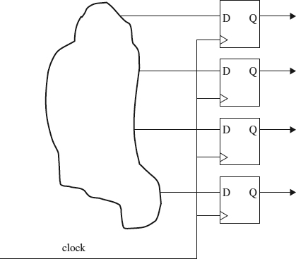
FIGURE 4.3. Diagram showing ideal connectivity of clock signal in a design.
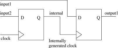
FIGURE 4.4. Diagram showing an output flip-flop driving another flip-flop.
The main advantage of having such a design is to allow the APR tool to perform its clock tree synthesis and insert clock buffers into the clock tree if needed. By doing so, the variable of clock skew can be ignored by the designer during HDL coding phase.
4.3.1 Internally Generated Clock
An internally generated clock should be used as little as possible. Ideally, synthesized designs should not have clocks that are internally generated.
Having synthesized designs that have flops or latches that are clocked internally complicates timing analysis. It is difficult to constrain the internal generated clock signal during synthesis.
Figure 4.4 is a diagram showing the output of a flip-flop being used to clock another flip-flop. Such a design can complicate the timing constraint process. Most synthesis and timing analysis tools have difficulties in identifying the type of internally generated clock design in Figure 4.4. Example 4.2 shows the Verilog code for the design in Figure 4.4.
Example 4.2 Verilog Code for the Design of Figure 4.4
module internal_clock (input1, input2, clock, output1);
input input1, input2, clock;
output output1;
reg internal,output1;

always @ (posedge clock)
begin
     internal <= input1;
end

always @ (posedge internal)
begin
     output1 <= input2;
end
endmodule
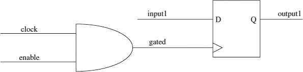
FIGURE 4.5. Diagram showing a gated clock driving a flip-flop.
4.3.2 Gated Clock
A design that has an enable signal to enable an internal clock, based on a global clock is called “gated clock.” The term refers to the fact that the global clock is gated with a signal to generate the internal clock.
Gated clock designs are normally used when a designer wishes to switch off the clock signal under certain conditions. This could be for the purpose of power-saving features. Figure 4.5 shows an example of a design that has a flip-flop being clocked by a gated clock signal generated from an AND condition of “enable” and “clock.”
Referring to the example in Figure 4.5, several ways can be used to code the design. The most common method is using boolean assignment and gate instantiation. Example 4.3 shows the Verilog code using boolean assignment. Example 4.4 shows the Verilog code using the gate instantiation method.
Example 4.3 Verilog Code for Gated Clock Design Using BOOLEAN Assignment
module gated_clock (input1, enable, clock, output1);
input input1, clock, enable;
output output1;
wire gated;
reg output1;

assign gated = clock & enable;
always @ (posedge gated)
begin
   output1 <= input1;
end

endmodule
Example 4.4 Verilog Code for Gated Clock Design Using Gate Instantiation

Note: Example 4.4 assumes of a precompiled AND gate with inputs “I1” and “I2” and output “O”. Another method to instantiate an AND gate is to use the built-in Verilog primitive “and” (refer to Section 3.2): and AND_instance (O, I1, I2).
Of the two methods, gate instantiation is the preferred method to handle gated clock. This is advisable, as instantiating the gate for the gated clock would allow the designer more control on the fanout of the signal gated. For example, let's assume that the signal gated is to drive the clock of 32 flip-flops (Figure 4.6).
Referring to Figure 4.6, a fanout of 32 on signal gated is most likely to create a loading that is too heavy on the AND gate. As a result, the skew on the signal gated may be too large. Of course the designer can buffer up the signal gated during synthesis. However, buffering the signal gated is not recommended because it is a clock signal. Therefore, any buffering on the signal gated should be done only in APR (auto-place-route).
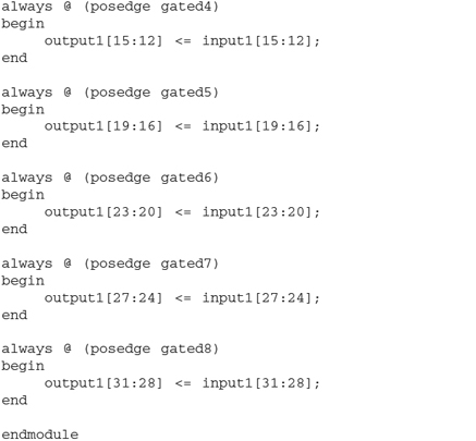
Therefore, a better approach would be the gate instantiation method. This method allows the designer to control the loading on the AND gate that drives the signal gated. Using the same example of Figure 4.6, the designer can break the signal gated into several signals. And each signal would drive only a limited amount of flip-flops (refer to Fig. 4.7).
Referring to Figure 4.7, the signal clock and signal enable are used to create eight separate signals gated, ranging from gated1 to gated8. Each gated signal only drives four flip-flops. To achieve this, the designer instantiates eight separate AND gates to create eight different gated signals. This method reduces the loading on each of the gated signal and allows the designer to achieve the required clock skew on signal gated. Example 4.5 shows the Verilog code for the gate instantiation method that allows a controlled clock skew on the signal gated (Fig. 4.7).

FIGURE 4.6. Diagram showing signal gated driving clock of 32 flip-flops.

FIGURE 4.7. Diagram showing multiple gated signal to drive 32 flip-flops.
Example 4.5 Verilog Code for Gated Clock Design Using Gate Instantiation to Drive 32 Flip-flops

4.4 RESET
Every design has some form of reset. It is a common requirement to allow a design to be “reset” to a certain known state during certain conditions.
There are two types of reset: asynchronous reset and synchronous reset. Both reset a design but their implications are very different.
4.4.1 Asynchronous Reset
Asynchronous reset is a reset that can occur at anytime. There is no reference of timing on this reset to any other signal. It can occur independent of any condition or other signal values. Figure 4.8 shows a simple design with a reset flip-flop. The output value of the flip-flop is a logical zero whenever the reset of the flip-flop is at a logical one. Example 4.6 is the Verilog code for a design example of asynchronous reset.

FIGURE 4.8. Diagram showing a design with an asynchronous reset flip-flop.
Example 4.6 Verilog Code for an Asynchronous Reset Design

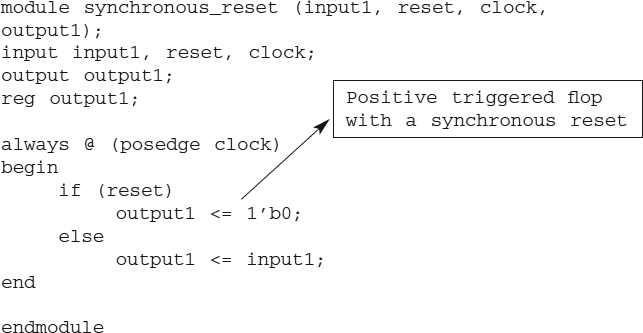
4.4.2 Synchronous Reset
Synchronous reset is a reset that can only occur at the rising edge of clock for a positive clock-triggered flip-flop and falling edge of clock for a negative clock-triggered flip-flop. This means that synchronous reset is only recognized during rising edge or falling edge of clock. In other words, synchronous reset is referenced to the clock signal. It cannot occur independent of the clock. Figure 4.9 shows a simple synchronous reset design. The output value of the flip-flop is updated during the rising edge of clock. The output value of the flip-flop is a logical zero, if during the rising edge of clock, reset is at logical one. The output value of the flip-flop is the logical value of the input data of the flip-flop, if reset is at logical zero during rising edge of clock. Example 4.7 shows the Verilog code for a design example of synchronous reset.

FIGURE 4.9. Diagram showing a design with a synchronous reset flip-flop.
Example 4.7 Verilog Code for a Synchronous Reset Design
4.5 TIMING LOOP
Timing loops are loops in a design that have an output from combinational logic being looped back to be part of the input of the combinational logic.
For designs that are synthesized, it is important that they do not have timing loops. If a design has such loops, timing analysis is made complicated because the output is being looped back to the input. Figure 4.10 shows an example of a design having timing loop. Notice how the output of the inverter is being looped back as an input to the AND gate.
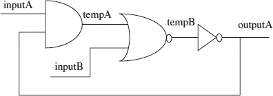
FIGURE 4.10. Diagram showing a design with timing loop.
When a design has timing loops, it is advisable that it be broken by a sequential element. This ensures that the timing loop, which may cause timing glitches, is broken into two timing paths: presequential and postsequential element path.
Note: The Verilog code for the logic circuit in Figure 4.10 uses outputA to be looped back to generate tempA.
module timingloop (inputA, inputB, outputA);
input inputA, inputB;
output outputA;
wire tempA, tempB;
assign tempA = inputA & outputA;
assign tempB = ~ (inputB | tempA);
assign outputA = ~tempB;
endmodule
It is not advisable for a designer to write Verilog code that uses timing loop. Logic circuits that have timing loops complicate timing analysis and have potential for causing timing glitches.
4.6 BLOCKING AND NONBLOCKING STATEMENTS
Blocking and nonblocking are two types of procedural assignments that are used in Verilog coding. Both of these types are used in sequential statements. Each of these blocking and nonblocking statements have different characteristics and behaviors.
Blocking statements are represented by the symbol “=”. When a blocking statement is used, the statement is executed before the simulator moves forward to the next statement. In other words, a blocking statement is truly sequential.
Nonblocking statements are represented by the symbol “<=”. When a nonblocking statement is used, that statement is scheduled and executed together with the other nonblocking assignments. What this means is that nonblocking allows several assignments to be scheduled and executed together, resulting in nonblocking statements that do not have dependence on the order in which the assignments occur (Examples 4.8 to 4.15 explain the difference between blocking and nonblocking statements in detail).
Do note that blocking and nonblocking statements refer only to Verilog code. VHDL code does not require concept of blocking and nonblocking.
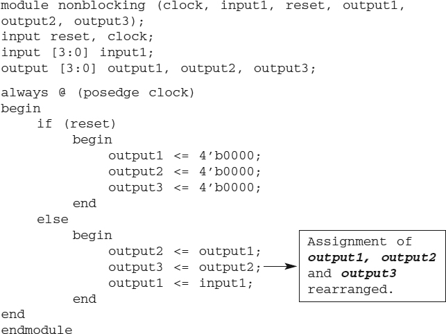
Example 4.8 shows Verilog code for a simple design using nonblocking statements. The module “non-blocking” is basically a synchronous reset register-based design.
Example 4.8 Verilog Code Showing Use of Nonblocking Statement
module nonblocking (clock, input1, reset, output1, output2, output3);
input reset, clock;
input [3:0] input1;
output [3:0] output1, output2, output3;

always @ (posedge clock)
begin
     if (reset)
          begin
               output1 <= 4'b0000;
               output2 <= 4'b0000;
               output3 <= 4'b0000;
          end
     else
          begin
               output1 <= input1;
               output2 <= output1;
               output3 <= output2;
          end
end
endmodule
Using the Verilog code of Example 4.8, Example 4.9 and Example 4.10 shows two other Verilog codes using nonblocking statements. Each Verilog code of Example 4.8, 4.9, and 4.10 uses a different order to assign values to output1, output2, and output3.
Example 4.9 Verilog Code for Example 4.8 with the Output Assignment Rearranged
![]()

Example 4.10 Verilog Code for Example 4.9 with the Output Assignment Rearranged
Notice how the Verilog code of Examples 4.8, 4.9, and 4.10 are basically the same except for the arrangement of sequence of assignment for output1, output2, and output3. A simple test bench is written to simulate all three of these examples. Example 4.11 shows the Verilog code for the test bench.
Example 4.11 Verilog Code for Test Bench for Simulation of Examples 4.8, 4.9, and 4.10
module nonblocking_tb ();

reg [3:0] input1;
reg clock, reset;
wire [3:0] output1, output2, output3;

initial
begin
     clock = 0;
     input1 = 0;
     forever #50 clock = ~clock;
end

initial
begin
     #10;
     reset = 0;
     #10;
     reset = 1;
     #10;
     reset = 0;
     #10;
     input1 = 1;
     #50;
     input1 = 2;
     #200;
     $finish;
end

nonblocking nonblocking_instance (clock, input1, reset, output1, output2, output3);

endmodule
Using the test bench shown in Example 4.11, the Verilog code for Examples 4.8, 4.9, and 4.10 is simulated. The simulation results are shown in Figures 4.11, 4.12, and 4.13.

FIGURE 4.11. Diagram showing simulation results of Verilog code in Example 4.8.

FIGURE 4.12. Diagram showing simulation results of Verilog code in Example 4.9.
Notice the simulation results shown in Figures 4.11, 4.12, and 4.13 are the same. Although the sequence of statement assignments of output1, output2, and output3 are different for the Verilog code of Examples 4.8, 4.9, and 4.10, the simulation results are the same. Changing the arrangement of the sequence of statement assignments does not affect simulation because the three examples uses nonblocking statements. This would mean that the assignment of “output1 ![]() input1,” “output2
input1,” “output2 ![]() output1, and “output3
output1, and “output3 ![]() output2” are executed together. Therefore, when using nonblocking statements, order dependence does not affect simulation results.
output2” are executed together. Therefore, when using nonblocking statements, order dependence does not affect simulation results.
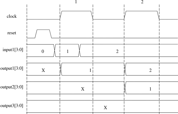
FIGURE 4.13. Diagram showing simulation results of Verilog code in Example 4.10.

FIGURE 4.14. Diagram showing simulation results of Verilog code in Example 4.12.
Referring to Figures 4.11, 4.12, and 4.13,
- The Verilog codes in Examples 4.8, 4.9, and 4.10 use a synchronous reset. Therefore, when reset is at logical “1”, output1, output2, and output3 are not reset to a value of “0” because a positive edge of clock did not occur.
- On the rising edge of the first clock, output1 is assigned the value of input1, which is decimal 1. Output2 is assigned the value of output1, which is X. Similarly output3 is assigned the value of output2, which is also X.
- On the rising edge of the second clock, output1 is assigned the value of input1, which is decimal 2. Output2 is assigned the value of output1, which is decimal 1. And output3 is assigned the value of output2, which is X.
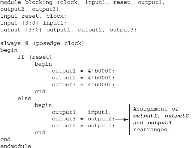
Examples 4.12, 4.13, and 4.14 are the same pieces of Verilog code as Examples 4.8, 4.9, and 4.10, but blocking statements are used instead of nonblocking statements.
Example 4.12 Verilog Code Showing Example 4.8 Using a Blocking Statement
module blocking (clock, input1, reset, output1, output2, output3);
input reset, clock;
input [3:0] input1;
output [3:0] output1, output2, output3;

always @ (posedge clock)
begin
     if (reset)
          begin
               output1 = 4'b0000;
               output2 = 4'b0000;
               output3 = 4'b0000;
          end
     else
          begin
               output1 = input1;
               output2 = output1;
               output3 = output2;
          end
end
endmodule
Example 4.13 Verilog Code Showing Example 4.9 Using a Blocking Statement
Example 4.14 Verilog Code Showing Example 4.10 Using Blocking Statement


Notice how the Verilog code of Examples 4.12, 4.13, and 4.14 are basically the same except for the arrangement of sequence of assignment for output1, output2, and output3. A testbench is written to simulate all three of these examples. Example 4.15 shows the Verilog code for the testbench. Also take note that the stimulus used in the testbench of Example 4.15 is the same set of stimulus used in the testbench of Example 4.11.
Example 4.15 Verilog Code for Testbench for Simulation of Examples 4.12, 4.13, and 4.14
module blocking_tb ();

reg [3:0] input1;
reg clock, reset;
wire [3:0] output1, output2, output3;

initial
begin
     clock = 0;
     input1 = 0;
     forever #50 clock = ~clock;
end

initial
begin
     #10;
     reset = 0;
     #10;
     reset = 1;
     #10;
     reset = 0;
     #10;
     input1 = 1;
     #50;
     input1 = 2;
     #200 ;
     $finish;
end
blocking blocking_instance (clock, input1, reset, output1, output2, output3);

endmodule
Using the test bench shown in Example 4.15, the Verilog code for Examples 4.12, 4.13, and 4.14 are simulated. The simulation results are shown in Figures 4.14, 4.15, and 4.16.
Referring to the simulation waveform in Figure 4.14:
- The Verilog code in Example 4.12 uses a synchronous reset. Therefore, when the reset is at logical “1”, output1, output2, and output3 are not reset to value of “0” because a positive edge of clock did not occur.
- On the rising edge of the first clock, output1 is assigned the value of input1, which is decimal 1. Output2 is assigned the value of output1. Because this is a blocking statement, the assignment of “output2 = output1” will only occur after the assignment of “output1 = input1” has completed. Thus, output2 has a value of decimal 1. Similarly, the assignment of “output3 = output2” only occurs after the assignment of “output2 = output1”. Because output2 has a value of decimal 1, output3 is also assigned a value of decimal 1.
- On the rising edge of the second clock, output1 is assigned the value of input1, which is a decimal 2. Output2 is assigned the value of output1. Because this is a blocking statement, the assignment of “output2 = output1” will only occur after the assignment of “output1 = input1” has completed. Thus, output2 has a value of decimal 2. Similarly, the assignment of “output3 = output2” only occurs after the assignment of “output2 = output1.” Because output2 has a value of decimal 2, output3 is also assigned a value of decimal 2.

FIGURE 4.15. Diagram showing simulation results of Verilog code in Example 4.13.

FIGURE 4.16. Diagram showing simulation results of Verilog code in Example 4.14.
Referring to the simulation waveform in Figure 4.15:
- The Verilog code in Example 4.13 uses a synchronous reset. Therefore, when reset is at logical “1,” output1, output2, and output3 are not reset to value of “0” because a positive edge of clock did not occur.
- On the rising edge of the first clock, output1 is assigned the value of input1, which is a decimal 1. Output3 is assigned the value of output2. Because this is a blocking statement, at the moment when the assignment of “output3 = output2” occurs, output2 is at X. Thus, output3 is also assigned X. For the assignment of “output2 = output1,” this blocking statement occurs after the assignments of “output1 = input1” and “output3 = output2” have occurred. Because output1 has already been assigned the value of decimal 1, output2 is also assigned the value of decimal 1.
- On the rising edge of the second clock, output1 is assigned the value of input1, which is a decimal 2. Output3 is assigned the value of output2, which is a decimal 1. For the assignment of “output2 = output1,” which is a blocking statement, this statement assignment only occurs after “output1 = input1” and “output3 = output2” have occurred. Therefore, output2 is assigned the value of decimal 1.
Referring to the simulation waveform in Figure 4.16:
- The Verilog code in Example 4.14 uses a synchronous reset. Therefore, when reset is at logical “1,” output1, output2, and output3 are not reset to value of “0” because a positive edge of clock did not occur.
- On the rising edge of the first clock, output2 is assigned the value of output1, which is X. Output3 is assigned the value of output2. At the moment when the assignment of “output3 = output2” occurs, output2 is at X. Therefore, output3 is also assigned X. For the assignment of “output1 = input1,” because input1 has a value of decimal 1, output1 is also assigned the value of decimal 1.
- On the rising edge of the second clock, output2 is assigned value of output1, which is a decimal 1. Output3 is assigned the value of output2, which is a decimal 1. For the assignment of “output1 = input1,” because input1 has a value of decimal 2, output1 is assigned the value of decimal 2.
Referring to simulation waveforms of Examples 4.12, 4.13, and 4.14 (Figs. 4.14, 4.15, and 4.16), it is obvious that use of a blocking statement within an “always @ (posedge” block gives different simulation results when the order of statement assignment is changed. In other words, use of a blocking statement is order dependent.
Referring to simulation waveforms of Examples 4.8, 4.9, and 4.10 (Figs. 4.11, 4.12, and 4.13), use of a nonblocking statement within an “always @ (posedge” block gives the same simulation results when the order of statement assignment is changed. In other words, use of a nonblocking statement is not order dependent.
From the exercise of Examples 4.8 to 4.15, it is concluded that nonblocking statements must be used when coding for registers. When coding for combinational logic, blocking statements are used. This ensures that when a designer is writing code to synthesize registers, the order in which the nonblocking statements are written will not affect simulation.
Note: When writing Verilog code that involves more than one register assignment, always use nonblocking statements. This will ensure that the order in which the register assignments is made does not affect the simulation results.
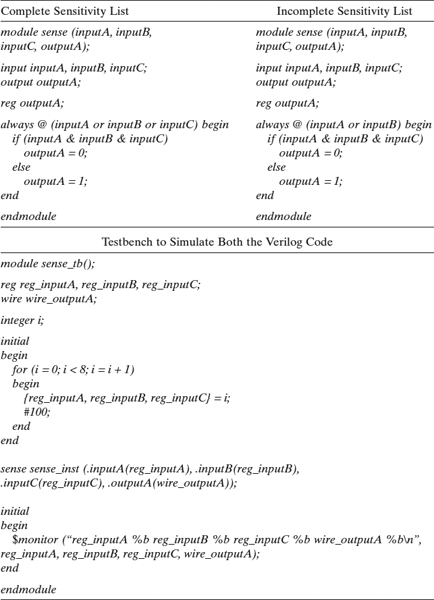
4.7 SENSITIVITY LIST
Verilog uses a sensitivity list to determine if a block of sequential statements needs to be evaluated by the simulator during certain simulation cycles. For Verilog, a sensitivity list is required for the always statement.
Example 4.16 shows a Verilog code for a design module that has an “always” block. This block is to be evaluated by the simulator whenever there is a change in the signals corresponding to the sensitivity list of the “always” block.
Example 4.16 Verilog Example Showing Sensitivity List for “always” Block

Referring to Example 4.16, the sensitivity list consists of three signals, X, Y, and Z. The block of sequential statements within the “always” block is evaluated by the simulator whenever there is a change of values in either signal X, Y, or Z.
An incomplete signal list in the sensitivity list for an “always” block may cause simulation results to be inaccurate. It may also cause a mismatch between the synthesis results of the Verilog code and the simulation results. It is therefore important to always keep note that signals evaluated in an “always” block needs to be included in the sensitivity list.
Table 4.1 is an example of the differences in simulation that may occur due to an incomplete senstivity list.
Notice how the simulation results for the modules differ. The result of outputA for the module that has incomplete sensitivity list has a logic value of “1” for all combinations of inputs inputA, inputB, and inputC. The module that has complete sensitivity list has the results of outputA at logic “0” when inputs inputA, inputB, and inputC are at a combination of “111.”
Both of the modules, although having different simulation results, when synthesized will generate a NAND gate. In this case, it is clear that that synthesized logic will never match the simulation result of the module with incomplete sensitivity list. It is therefore very important for a designer to always use a complete sensitivity list when using an always statement in Verilog.
TABLE 4.1. Differences in simulation resulting from an incomplete sensitivity list

4.8 VERILOG OPERATORS
Verilog allows the use of a large number of operators. Operators form the very basic components when coding for a design. It allows the designer to use these operators to achieve different functionalities and operations.
All Verilog operators are synthesizable. These operators can be grouped into different types, with each type having its own set of functionality.
4.8.1 Conditional Operators
Conditional operators are commonly used to model combinational logic designs that behave as a switching device. A conditional operator consists of three operands: (a) the input expression; (b) the select control signal that selects which input expression is to be passed through to the output; (c) the output expression.
The syntax for a conditional operator is as follows:
assign output_signal = control_signal ? input1 : input2;
whereby output_signal is the output of the conditional statement, control_signal is the signal that chooses whether input1 or input2 is passed to output_signal (if control_signal is true, input1 is passed to output_signal, otherwise, input2).
TABLE 4.2. Truth table showing functionality for module “conditional”
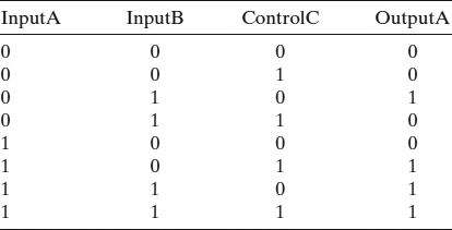
Table 4.2 is a truth table that shows the functionality of a module called “conditional,” which can be modeled in Verilog using the conditional operator.
Example 4.17 shows the Verilog code for module “conditional,” which has the functionality of Table 4.2.
Example 4.17 Verilog Code for Module “conditional”
module conditional (inputA, inputB, controlC, outputA);

input inputA, inputB, controlC;
output outputA;

wire outputA;

assign outputA = controlC ? inputA : inputB;

endmodule
When Example 4.17 is synthesized, Figure 4.17 is obtained. The logic synthesized from Example 4.17 is a multiplexer. Therefore, when coding for synthesis, a good method to code for multiplexers is to use conditional operators.
4.8.2 Bus Concatenation Operator
Multiple signals can be concatenated to form a bus. This can be achieved by using the bus concatenation operator. The syntax on using this operator is
assign signal_bus = {signal1, signal2, signal3};

FIGURE 4.17. Diagram showing synthesized logic for module “conditional.”
whereby signal_bus is the name of the three-bit concatenated bus and signal1, signal2, and signal3 are the signals concatenated together.
Example 4.18 Verilog Example Showing a Three-Bit and Four-Bit Bus Concatenation

Example 4.18 shows a Verilog code that concatenates three signals, inputA, inputB, and inputC, into a three-bit bus outputA and the concatenation of four signals, inputA, inputB, inputC, and inputD into a four-bit bus outputB.
4.8.3 Shift Operator
Shift operations can be performed in Verilog by using the shift left operator for shifting a bus to the left or a shift right operator for shifting a bus to the right.
Example 4.19 shows a Verilog code that uses the shift left operator to shift the three-bit bus signal tempA by one bit to the left.
Example 4.19 Verilog Code Using the Shift Left Operator

When the Verilog code of Example 4.19 is synthesized, the logic obtained is illustrated in Figure 4.18.
Example 4.20 shows the Verilog code for a test bench that can be used to simulate the Verilog code of module “shift_left” to verify that the logic obtained is as shown in Figure 4.18.
Example 4.20 Verilog Code for Test Bench to Simulate Module “shift_left”


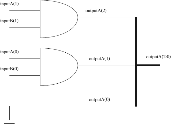
FIGURE 4.18. Diagram showing synthesized logic for module “shift_left.”
Example 4.21 shows the simulation results of the test bench module “shift_left_tb”.
Example 4.21 Simulation Results of Test Bench Module “shift_left_tb”
inputA 000 inputB 000 tempA 000 outputA 000
inputA 000 inputB 001 tempA 000 outputA 000
inputA 000 inputB 010 tempA 000 outputA 000
inputA 000 inputB 011 tempA 000 outputA 000
inputA 000 inputB 100 tempA 000 outputA 000
inputA 000 inputB 101 tempA 000 outputA 000
inputA 000 inputB 110 tempA 000 outputA 000
inputA 000 inputB 111 tempA 000 outputA 000
inputA 001 inputB 000 tempA 000 outputA 000
inputA 001 inputB 001 tempA 001 outputA 010
inputA 001 inputB 010 tempA 000 outputA 000
inputA 001 inputB 011 tempA 001 outputA 010
inputA 001 inputB 100 tempA 000 outputA 000
inputA 001 inputB 101 tempA 001 outputA 010
inputA 001 inputB 110 tempA 000 outputA 000
inputA 001 inputB 111 tempA 001 outputA 010
inputA 010 inputB 000 tempA 000 outputA 000
inputA 010 inputB 001 tempA 000 outputA 000
inputA 010 inputB 010 tempA 010 outputA 100
inputA 010 inputB 011 tempA 010 outputA 100
inputA 010 inputB 100 tempA 000 outputA 000
inputA 010 inputB 101 tempA 000 outputA 000
inputA 010 inputB 110 tempA 010 outputA 100
inputA 010 inputB 111 tempA 010 outputA 100
inputA 011 inputB 000 tempA 000 outputA 000
inputA 011 inputB 001 tempA 001 outputA 010
inputA 011 inputB 010 tempA 010 outputA 100
inputA 011 inputB 011 tempA 011 outputA 110
inputA 011 inputB 100 tempA 000 outputA 000
inputA 011 inputB 101 tempA 001 outputA 010
inputA 011 inputB 110 tempA 010 outputA 100
inputA 011 inputB 111 tempA 011 outputA 110
inputA 100 inputB 000 tempA 000 outputA 000
inputA 100 inputB 001 tempA 000 outputA 000
inputA 100 inputB 010 tempA 000 outputA 000
inputA 100 inputB 011 tempA 000 outputA 000
inputA 100 inputB 100 tempA 100 outputA 000
inputA 100 inputB 101 tempA 100 outputA 000
inputA 100 inputB 110 tempA 100 outputA 000
inputA 100 inputB 111 tempA 100 outputA 000
inputA 101 inputB 000 tempA 000 outputA 000
inputA 101 inputB 001 tempA 001 outputA 010
inputA 101 inputB 010 tempA 000 outputA 000
inputA 101 inputB 011 tempA 001 outputA 010
inputA 101 inputB 100 tempA 100 outputA 000
inputA 101 inputB 101 tempA 101 outputA 010
inputA 101 inputB 110 tempA 100 outputA 000
inputA 101 inputB 111 tempA 101 outputA 010
inputA 110 inputB 000 tempA 000 outputA 000
inputA 110 inputB 001 tempA 000 outputA 000
inputA 110 inputB 010 tempA 010 outputA 100
inputA 110 inputB 011 tempA 010 outputA 100
inputA 110 inputB 100 tempA 100 outputA 000
inputA 110 inputB 101 tempA 100 outputA 000
inputA 110 inputB 110 tempA 110 outputA 100
inputA 110 inputB 111 tempA 110 outputA 100
inputA 111 inputB 000 tempA 000 outputA 000
inputA 111 inputB 001 tempA 001 outputA 010
inputA 111 inputB 010 tempA 010 outputA 100
inputA 111 inputB 011 tempA 011 outputA 110
inputA 111 inputB 100 tempA 100 outputA 000
inputA 111 inputB 101 tempA 101 outputA 010
inputA 111 inputB 110 tempA 110 outputA 100
inputA 111 inputB 111 tempA 111 outputA 110
Note: Notice from the simulation results that the (LSB) is always a zero? This occurs because, when shifting left, the LSB is always tagged with logic zero. This causes the synthesized logic for module shift_left to have the outputA(0) grounded.
Example 4.22 shows a Verilog code that uses the shift right operator to shift the three-bit bus signal tempA by one bit to the right.
Example 4.22 Verilog Code Using the Shift Right Operator

When the Verilog code of Example 4.22 is synthesized, the logic obtained is illustrated in Figure 4.19.

FIGURE 4.19. Diagram showing synthesized logic for module “shift_right.”
Example 4.23 shows the Verilog code for a test bench that can be used to simulate the verilog code of module “shift_right” to verify that the logic obtained is as shown in Figure 4.19.
Example 4.23 Verilog Code for Test Bench to Simulate Module “shift_right”
module shift_right_tb();

reg [2:0] reg_inputA, reg_inputB;
wire [2:0] wire_outputA;

integer i,j;

initial
begin
    for (i=0; i<8; i=i+1)
        begin
            // to force input stimulus for inputA
            reg_inputA = i;
            for (j=0; j<8; j=j+1)
                begin
                    // to force input stimulus for inputB
                    reg_inputB = j;
                    #10;
                end
        end
end

shift_right shift_right_inst (.inputA(reg_inputA), .inputB(reg_inputB), .outputA(wire_outputA));

initial
begin
     $monitor ("inputA %b%b%b inputB %b%b%b tempA %b%b%b outputA %b%b%b",reg_inputA[2], reg_inputA[1], reg_inputA[0], reg_inputB[2], reg_inputB[1], reg_inputB[0], shift_right_inst.tempA[2], shift_right_inst.tempA[1], shift_right_ inst.tempA[0], wire_outputA[2], wire_outputA[1], wire_outputA[0]);
end

endmodule
Example 4.24 shows the simulation results of the test bench module “shift_right_tb.”
Example 4.24 Simulation Results of Verilog Test Bench Module “shift_right_tb”
inputA 000 inputB 000 tempA 000 outputA 000
inputA 000 inputB 001 tempA 000 outputA 000
inputA 000 inputB 010 tempA 000 outputA 000
inputA 000 inputB 011 tempA 000 outputA 000
inputA 000 inputB 100 tempA 000 outputA 000
inputA 000 inputB 101 tempA 000 outputA 000
inputA 000 inputB 110 tempA 000 outputA 000
inputA 000 inputB 111 tempA 000 outputA 000
inputA 001 inputB 000 tempA 000 outputA 000
inputA 001 inputB 001 tempA 001 outputA 000
inputA 001 inputB 010 tempA 000 outputA 000
inputA 001 inputB 011 tempA 001 outputA 000
inputA 001 inputB 100 tempA 000 outputA 000
inputA 001 inputB 101 tempA 001 outputA 000
inputA 001 inputB 110 tempA 000 outputA 000
inputA 001 inputB 111 tempA 001 outputA 000
inputA 010 inputB 000 tempA 000 outputA 000
inputA 010 inputB 001 tempA 000 outputA 000
inputA 010 inputB 010 tempA 010 outputA 001
inputA 010 inputB 011 tempA 010 outputA 001
inputA 010 inputB 100 tempA 000 outputA 000
inputA 010 inputB 101 tempA 000 outputA 000
inputA 010 inputB 110 tempA 010 outputA 001
inputA 010 inputB 111 tempA 010 outputA 001
inputA 011 inputB 000 tempA 000 outputA 000
inputA 011 inputB 001 tempA 001 outputA 000
inputA 011 inputB 010 tempA 010 outputA 001
inputA 011 inputB 011 tempA 011 outputA 001
inputA 011 inputB 100 tempA 000 outputA 000
inputA 011 inputB 101 tempA 001 outputA 000
inputA 011 inputB 110 tempA 010 outputA 001
inputA 011 inputB 111 tempA 011 outputA 001
inputA 100 inputB 000 tempA 000 outputA 000
inputA 100 inputB 001 tempA 000 outputA 000
inputA 100 inputB 010 tempA 000 outputA 000
inputA 100 inputB 011 tempA 000 outputA 000
inputA 100 inputB 100 tempA 100 outputA 010
inputA 100 inputB 101 tempA 100 outputA 010
inputA 100 inputB 110 tempA 100 outputA 010
inputA 100 inputB 111 tempA 100 outputA 010
inputA 101 inputB 000 tempA 000 outputA 000
inputA 101 inputB 001 tempA 001 outputA 000
inputA 101 inputB 010 tempA 000 outputA 000
inputA 101 inputB 011 tempA 001 outputA 000
inputA 101 inputB 100 tempA 100 outputA 010
inputA 101 inputB 101 tempA 101 outputA 010
inputA 101 inputB 110 tempA 100 outputA 010
inputA 101 inputB 111 tempA 101 outputA 010
inputA 110 inputB 000 tempA 000 outputA 000
inputA 110 inputB 001 tempA 000 outputA 000
inputA 110 inputB 010 tempA 010 outputA 001
inputA 110 inputB 011 tempA 010 outputA 001
inputA 110 inputB 100 tempA 100 outputA 010
inputA 110 inputB 101 tempA 100 outputA 010
inputA 110 inputB 110 tempA 110 outputA 011
inputA 110 inputB 111 tempA 110 outputA 011
inputA 111 inputB 000 tempA 000 outputA 000
inputA 111 inputB 001 tempA 001 outputA 000
inputA 111 inputB 010 tempA 010 outputA 001
inputA 111 inputB 011 tempA 011 outputA 001
inputA 111 inputB 100 tempA 100 outputA 010
inputA 111 inputB 101 tempA 101 outputA 010
inputA 111 inputB 110 tempA 110 outputA 011
inputA 111 inputB 111 tempA 111 outputA 011
Note: Notice from the simulation results that the (MSB) is always a zero? This occurs because when shifting right, the MSB is always tagged with logic zero. This causes the synthesized logic for module shift_right to have the outputA(2) grounded.
4.8.4 Arithmetic Operator
Verilog allows for five different arithmetic operators that can be used for different operations. They are as follows:
- addition operator
- subtraction operator
- multiplication operator
- division operator
- modulus operator
When using these operators, the designer needs to be aware that the logic solution obtained from synthesis may differ if different design constraints are used.
4.8.4.1 Addition operator As the name implies, the addition operator allows an addition operation. It is coded in Verilog by using the symbol “+”.
Example 4.25 Verilog Code Using an Addition Operator
module addition (inputA, inputB, outputA);

input inputA, inputB;
output [1:0] outputA;

wire [1:0] outputA;

assign outputA = inputA + inputB;

endmodule
Figure 4.20 shows a diagram of the synthesized logic module “addition” in Example 4.25.
Example 4.26 is a Verilog test bench that can be used to simulate the Verilog code of module “addition.” The simulation results are shown in Example 4.27.
Example 4.26 Verilog Test Bench to Simulate Verilog Code for Module “addition”
module addition_tb ();

reg reg_inputA, reg_inputB;

wire [1:0] wire_outputA;

integer i,j;

initial
begin
     for (i=0; i<2; i=i+1)
     begin
          reg_inputA = i;
          for (j=0; j<2; j=j+1)
               begin
                    reg_inputB = j;
                    #10;
              end
     end
end
addition addition_inst (.inputA(reg_inputA),
.inputB(reg_inputB), .outputA(wire_outputA));

initial
begin
     $monitor ("inputA %b inputB %b outputA %b%b", reg_inputA, reg_inputB, wire_outputA[1], wire_outputA[0]);
end

endmodule

Figure 4.20. Diagram showing synthesized logic for module “addition.”
Example 4.27 Simulation Results for Verilog Test Bench Module “addition_tb”
inputA 0 inputB 0 outputA 00
inputA 0 inputB 1 outputA 01
inputA 1 inputB 0 outputA 01
inputA 1 inputB 1 outputA 10
Appendix A.1 shows the Verilog code for a two-bit by two-bit adder design that uses an addition operator. It also includes a Verilog test bench, simulation results, and the synthesized logic circuit.
4.8.4.2 Subtraction operator As the name implies, the subtraction operator allows a subtract operation. It is coded in Verilog by using the symbol “−”.
Example 4.28 Verilog Code Using a Subtraction Operator
module subtraction (inputA, inputB, outputA);

input inputA, inputB;
output [1:0] outputA;

wire [1:0] outputA;

assign outputA = inputA - inputB;

endmodule
Figure 4.21 shows a diagram of the synthesized logic module “subtraction” in Example 4.28.
Example 4.29 is a Verilog test bench that can be used to simulate the Verilog code of module “subtraction.” The simulation results are shown in Example 4.30.
Example 4.29 Verilog Test Bench to Simulate Verilog Code for Module “subtraction”
module subtraction_tb ();

reg reg_inputA, reg_inputB;

wire [1:0] wire_outputA;

integer i,j;
initial
begin
     for (i=0; i<2; i=i+1)
          begin
               reg_inputA = i;
               for (j=0; j<2; j=j+1)
                   begin
                         reg_inputB = j;
                         #10;
                   end
          end
end

subtraction subtraction_inst (.inputA(reg_inputA),
.inputB(reg_inputB), .outputA(wire_outputA));

initial
begin
     $monitor ("inputA %b inputB %b outputA %b%b", reg_inputA, reg_inputB, wire_outputA[1], wire_outputA[0]);
end

endmodule

Figure 4.21. Diagram showing synthesized logic for module “subtraction.”
Example 4.30 Simulation Results for Verilog Test Bench Module “subtraction_tb”

Appendix A.2 shows the Verilog code for a two-bit by two-bit subtractor design that uses a subtraction operator. It also includes a Verilog test bench, simulation results, and the synthesized logic circuit.
4.8.4.3 Multiplication Operator As the name implies, the multiplication operator allows a multiplication operation. It is coded in Verilog by using the symbol “*”.
Example 4.31 Verilog Code Using a Multiplication Operator
module multiplication (inputA, inputB, outputA);

input [1:0] inputA, inputB;
output [3:0] outputA;

wire [3:0] outputA;

assign outputA = inputA * inputB;

endmodule
Figure 4.22 shows a diagram of the synthesized logic module “multiplication” in Example 4.31.
Example 4.32 is a Verilog test bench that can be used to simulate the Verilog code of module “multiplication.” The simulation results are shown in Example 4.33.

Figure 4.22. Diagram showing synthesized logic for module “multiplication”.
Example 4.32 Verilog Test Bench to Simulate Verilog Code for Module “multiplication”
module multiplication_tb ();

reg [1:0] reg_inputA, reg_inputB;

wire [3:0] wire_outputA;

integer i,j;

initial
begin
     for (i=0; i<4; i=i+1)
          begin
               reg_inputA = i;
               for (j=0; j<4; j=j+1)
                   begin
                         reg_inputB = j;
                         #10;
                   end
          end
end

multiplication multiplication_inst
(.inputA(reg_inputA), .inputB(reg_inputB),
.outputA(wire_outputA));

initial
begin
     $monitor ("inputA %h inputB %h outputA %h", reg_inputA, reg_inputB, wire_outputA);
end

endmodule
Example 4.33 Simulation Results for Verilog Test Bench Module “multiplication_tb”
inputA 0 inputB 0 outputA 0
inputA 0 inputB 1 outputA 0
inputA 0 inputB 2 outputA 0
inputA 0 inputB 3 outputA 0
inputA 1 inputB 0 outputA 0
inputA 1 inputB 1 outputA 1
inputA 1 inputB 2 outputA 2
inputA 1 inputB 3 outputA 3
inputA 2 inputB 0 outputA 0
inputA 2 inputB 1 outputA 2
inputA 2 inputB 2 outputA 4
inputA 2 inputB 3 outputA 6
inputA 3 inputB 0 outputA 0
inputA 3 inputB 1 outputA 3
inputA 3 inputB 2 outputA 6
inputA 3 inputB 3 outputA 9
Appendix A.3 shows the Verilog code for a four-bit by four-bit multiplier design that uses a multiplication operator. It also includes a Verilog test bench and simulation results.
4.8.5 Division Operator
As the name implies, the division operator allows a division operation. It is coded in Verilog by using the symbol “/”. The designer needs to be careful when using the division operator in synthesizable Verilog. The division operator can only be used on constants and not on variables. If the division operator is being used on a value that is not a constant, the synthesis tool will not be able to synthesize the logic.
Example 4.34 Verilog Code Using a Division Operator


Figure 4.23. Diagram showing synthesized logic for design module “division.”
Figure 4.23 shows a diagram for synthesized logic module “division.”
Example 4.35 is a Verilog test bench that can be used to simulate the Verilog code of module “division”. The simulation results are shown in Example 4.36.
Example 4.35 Verilog Test Bench to Simulate Verilog Code for Module “division”
module division_tb ();

reg [3:0] reg_inputA, reg_inputB;

wire [3:0] wire_outputA, wire_outputB;

integer i,j;

initial
begin
for (i=1; i<16; i=i+1)
          begin
               reg_inputA = i;
               for (j=1; j<16; j=j+1)
                    begin
                         reg_inputB = j;
                         #10;
                    end
          end
end

division division_inst (.inputA(reg_inputA),
.inputB(reg_inputB), .outputA(wire_outputA),
.outputB(wire_outputB));

initial
begin
     $monitor ("inputA %h inputB %h outputA %h outputB %h", reg_inputA, reg_inputB, wire_outputA, wire_outputB);
end

endmodule
Example 4.36 Simulation Results for Verilog Test Bench Module “division”


Note: Only constant values can be used when using the division operator in synthesizable Verilog code. Values obtained using the division operator are in integer format and do not have any fractions.
4.8.6 Modulus Operator
Modulus operator allows an arithmetic operation that returns a value of the remainder of a division (the operator is coded in Verilog by using the symbol “%”). For example, a modulus operation of “5 % 3” would return a value of 2, which is the remainder of the division operation of “5/3”.
The designer needs to be careful when using the modulus operator in synthesizable Verilog. The operator can only be used on constants and not on variables. If the modulus operator is being used on a value that is not a constant, the synthesis tool will not be able to synthesize the logic.
Example 4.37 Verilog Code Using a Modulus Operator
module modulus (inputA, inputB, outputA, outputB);

input [3:0] inputA;
input [3:0] inputB;
output [3:0] outputA, outputB;

reg [3:0] outputA, outputB;

always @ (inputA or inputB)
begin
     if (inputA == 4'b1010)
          outputA = 2 % 5;
     else
          outputA = 0;
     if (inputB == 4'b0011)
          outputB = 8 % 5;
     else
          outputB = 0;
end
endmodule
Figure 4.24 shows a diagram of the synthesized logic module “modulus.”
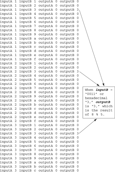
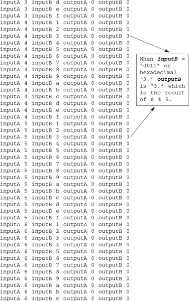
Example 4.38 is a verilog test bench that can be used to simulate the verilog code of module “ modulus”. The simulation results are shown in Example 4.39.
Example 4.38 Verilog Test Bench to Simulate Verilog Code for Module “modulus”
module modulus_tb ();

reg [3:0] reg_inputA, reg_inputB;

wire [3:0] wire_outputA, wire_outputB;

integer i,j;

initial
begin
      for (i=1; i<16; i=i+1)
           begin
                reg_inputA = i;
                for (j=1; j<16; j=j+1)
                     begin
                           reg_inputB = j;
                           #10;
                      end
           end
end
modulus modulus_inst (.inputA(reg_inputA), .inputB(reg_inputB), .outputA(wire_outputA), .outputB(wire_outputB));

initial
begin
     $monitor ("inputA %h inputB %h outputA %h outputB %h", reg_inputA, reg_inputB, wire_outputA, wire_outputB);
end
endmodule

Figure 4.24. Diagram showing synthesized logic for design module “modulus.”
Example 4.39 Simulation Results for Verilog Test Bench Module “modulus”


4.8.7 Logical Operator
Logical operators operate on a group of operands and return the result of the operation as a single-bit result of either 1 or 0. The operands can be single bit or multiple bit, but the result of the operation is always in single bit of 1 (true condition) or 0 (false condition). There are three different logical operators that can be used in Verilog:
- && This is a logical-AND operator. It performs an AND function on the operands to return a single-bit value.
 This is a logical-OR operator. It performs an OR function on the operands to return a single-bit value.
- ! This is a logical-NOT operator. It performs an inversion (NOT function) on the operand to return a single-bit value.
Example 4.40 shows a Verilog code that uses logical operators. The diagram in Figure 4.25 shows the synthesized logic for the Verilog code of module “logical” in Example 4.40.

FIGURE 4.25. Diagram showing synthesized logic for verilog code module “logical.”
Example 4.40 Verilog Code Using Logical Operators

Referring to Figure 4.25, notice how the output bus outputD(2:0) has bits (2:1) grounded whereas bit (0) is connected to logical gates. The outputD(2:1) is grounded because the logical operator returns a result that is only one bit wide, which represents either a true (logic 1) or false (logic 0) condition. Although inputD is a three-bit bus operand,
assign outputD = {inputA, inputB, inputC} && inputD;
concatenation of inputA, inputB, and inputC is also a three-bit bus, the result of outputD is only a single bit. The two upper bits of 1 and 2 are grounded.
Example 4.41 is a Verilog test bench that can be used to simulate the design module “logical” in Example 4.40. Example 4.42 shows the simulation results from the test bench.
Example 4.41 Verilog Test Bench for Simulating Module “logical”
module logical_tb ();

reg inputA, inputB, inputC;
reg [2:0] inputD;

integer i,j;

initial
begin
     for (i=0; i<8; i=i+1)
          begin
               {inputA, inputB, inputC} = i;
               for (j=0; j<8; j=j+1)
                    begin
                         inputD = j ;
                         #10;
                    end
          end
end
logical logical_inst (.inputA(inputA), .inputB(inputB), .inputC(inputC), .inputD(inputD), .outputA(outputA), .outputB(outputB), .outputC(outputC), .outputD(outputD));

initial
begin
     $monitor ("inputA %b inputB %b inputC %b inputD %h outputA %b outputB %b outputC %b outputD %h",inputA, inputB, inputC, inputD, outputA, outputB, outputC, outputD);
end

endmodule
Example 4.42 Simulation Results for Verilog Test Bench Module “logical_tb”
inputA 0 inputB 0 inputC 0 inputD 0 outputA 0 outputB 0 outputC 1 outputD 0
inputA 0 inputB 0 inputC 0 inputD 1 outputA 0 outputB 0 outputC 1 outputD 0
inputA 0 inputB 0 inputC 0 inputD 2 outputA 0 outputB 0 outputC 1 outputD 0
inputA 0 inputB 0 inputC 0 inputD 3 outputA 0 outputB 0 outputC 1 outputD 0
inputA 0 inputB 0 inputC 0 inputD 4 outputA 0 outputB 0 outputC 1 outputD 0
inputA 0 inputB 0 inputC 0 inputD 5 outputA 0 outputB 0 outputC 1 outputD 0
inputA 0 inputB 0 inputC 0 inputD 6 outputA 0 outputB 0 outputC 1 outputD 0
inputA 0 inputB 0 inputC 0 inputD 7 outputA 0 outputB 0 outputC 1 outputD 0
inputA 0 inputB 0 inputC 1 inputD 0 outputA 0 outputB 0 outputC 0 outputD 0
inputA 0 inputB 0 inputC 1 inputD 1 outputA 0 outputB 0 outputC 0 outputD 1
inputA 0 inputB 0 inputC 1 inputD 2 outputA 0 outputB 0 outputC 0 outputD 1
inputA 0 inputB 0 inputC 1 inputD 3 outputA 0 outputB 0 outputC 0 outputD 1
inputA 0 inputB 0 inputC 1 inputD 4 outputA 0 outputB 0 outputC 0 outputD 1
inputA 0 inputB 0 inputC 1 inputD 5 outputA 0 outputB 0 outputC 0 outputD 1
inputA 0 inputB 0 inputC 1 inputD 6 outputA 0 outputB 0 outputC 0 outputD 1
inputA 0 inputB 0 inputC 1 inputD 7 outputA 0 outputB 0 outputC 0 outputD 1
inputA 0 inputB 1 inputC 0 inputD 0 outputA 0 outputB 1 outputC 1 outputD 0
inputA 0 inputB 1 inputC 0 inputD 1 outputA 0 outputB 1 outputC 1 outputD 1
inputA 0 inputB 1 inputC 0 inputD 2 outputA 0 outputB 1 outputC 1 outputD 1
inputA 0 inputB 1 inputC 0 inputD 3 outputA 0 outputB 1 outputC 1 outputD 1
inputA 0 inputB 1 inputC 0 inputD 4 outputA 0 outputB 1 outputC 1 outputD 1
inputA 0 inputB 1 inputC 0 inputD 5 outputA 0 outputB 1 outputC 1 outputD 1
inputA 0 inputB 1 inputC 0 inputD 6 outputA 0 outputB 1 outputC 1 outputD 1
inputA 0 inputB 1 inputC 0 inputD 7 outputA 0 outputB 1 outputC 1 outputD 1
inputA 0 inputB 1 inputC 1 inputD 0 outputA 0 outputB 1 outputC 0 outputD 0
inputA 0 inputB 1 inputC 1 inputD 1 outputA 0 outputB 1 outputC 0 outputD 1
inputA 0 inputB 1 inputC 1 inputD 2 outputA 0 outputB 1 outputC 0 outputD 1
inputA 0 inputB 1 inputC 1 inputD 3 outputA 0 outputB 1 outputC 0 outputD 1
inputA 0 inputB 1 inputC 1 inputD 4 outputA 0 outputB 1 outputC 0 outputD 1
inputA 0 inputB 1 inputC 1 inputD 5 outputA 0 outputB 1 outputC 0 outputD 1
inputA 0 inputB 1 inputC 1 inputD 6 outputA 0 outputB 1 outputC 0 outputD 1
inputA 0 inputB 1 inputC 1 inputD 7 outputA 0 outputB 1 outputC 0 outputD 1
inputA 1 inputB 0 inputC 0 inputD 0 outputA 0 outputB 1 outputC 1 outputD 0
inputA 1 inputB 0 inputC 0 inputD 1 outputA 0 outputB 1 outputC 1 outputD 1
inputA 1 inputB 0 inputC 0 inputD 2 outputA 0 outputB 1 outputC 1 outputD 1
inputA 1 inputB 0 inputC 0 inputD 3 outputA 0 outputB 1 outputC 1 outputD 1
inputA 1 inputB 0 inputC 0 inputD 4 outputA 0 outputB 1 outputC 1 outputD 1
inputA 1 inputB 0 inputC 0 inputD 5 outputA 0 outputB 1 outputC 1 outputD 1
inputA 1 inputB 0 inputC 0 inputD 6 outputA 0 outputB 1 outputC 1 outputD 1
inputA 1 inputB 0 inputC 0 inputD 7 outputA 0 outputB 1 outputC 1 outputD 1
inputA 1 inputB 0 inputC 1 inputD 0 outputA 0 outputB 1 outputC 0 outputD 0
inputA 1 inputB 0 inputC 1 inputD 1 outputA 0 outputB 1 outputC 0 outputD 1
inputA 1 inputB 0 inputC 1 inputD 2 outputA 0 outputB 1 outputC 0 outputD 1
inputA 1 inputB 0 inputC 1 inputD 3 outputA 0 outputB 1 outputC 0 outputD 1
inputA 1 inputB 0 inputC 1 inputD 4 outputA 0 outputB 1 outputC 0 outputD 1
inputA 1 inputB 0 inputC 1 inputD 5 outputA 0 outputB 1 outputC 0 outputD 1
inputA 1 inputB 0 inputC 1 inputD 6 outputA 0 outputB 1 outputC 0 outputD 1
inputA 1 inputB 0 inputC 1 inputD 7 outputA 0 outputB 1 outputC 0 outputD 1
inputA 1 inputB 1 inputC 0 inputD 0 outputA 1 outputB 1 outputC 1 outputD 0
inputA 1 inputB 1 inputC 0 inputD 1 outputA 1 outputB 1 outputC 1 outputD 1
inputA 1 inputB 1 inputC 0 inputD 2 outputA 1 outputB 1 outputC 1 outputD 1
inputA 1 inputB 1 inputC 0 inputD 3 outputA 1 outputB 1 outputC 1 outputD 1
inputA 1 inputB 1 inputC 0 inputD 4 outputA 1 outputB 1 outputC 1 outputD 1
inputA 1 inputB 1 inputC 0 inputD 5 outputA 1 outputB 1 outputC 1 outputD 1
inputA 1 inputB 1 inputC 0 inputD 6 outputA 1 outputB 1 outputC 1 outputD 1
inputA 1 inputB 1 inputC 0 inputD 7 outputA 1 outputB 1 outputC 1 outputD 1
inputA 1 inputB 1 inputC 1 inputD 0 outputA 1 outputB 1 outputC 0 outputD 0
inputA 1 inputB 1 inputC 1 inputD 1 outputA 1 outputB 1 outputC 0 outputD 1
inputA 1 inputB 1 inputC 1 inputD 2 outputA 1 outputB 1 outputC 0 outputD 1
inputA 1 inputB 1 inputC 1 inputD 3 outputA 1 outputB 1 outputC 0 outputD 1
inputA 1 inputB 1 inputC 1 inputD 4 outputA 1 outputB 1 outputC 0 outputD 1
inputA 1 inputB 1 inputC 1 inputD 5 outputA 1 outputB 1 outputC 0 outputD 1
inputA 1 inputB 1 inputC 1 inputD 6 outputA 1 outputB 1 outputC 0 outputD 1
inputA 1 inputB 1 inputC 1 inputD 7 outputA 1 outputB 1 outputC 0 outputD 1
Referring to the simulation results shown in Example 4.42, note that the bus assignment to create outputD (assign outputD = {inputA, inputB, inputC} && inputD;) has a logical function that has outputD(0) at a logical 1 when any of inputA, inputB, inputC is a logical 1 AND any of the three bits of inputD is a logical 1.
4.8.8 Bitwise Operator
Bitwise operators are similar to logical operators except that bitwise operators operate on buses and return the logic result in bus form. For example, if a bitwise operator is used on two three-bit operands, the result of the operation would be a three-bit result. There are four types of bitwise operators:
- & This is a bitwise-AND operator. It performs an AND function on the operands to return a value that is equivalent in bus width to the operands.
- | This is a bitwise-OR operator. It performs an OR function on the operands to return a value that is equivalent in bus width to the operands.
- ~ This is a bitwise-NOT operator. It performs an inversion (NOT function) on the operand to return a value that is equivalent in bus width to the operands.
 This is a bitwise-XOR operator. It performs an XOR function on the operands to return a value that is equivalent in bus width to the operands.
Example 4.43 shows a Verilog code that uses bitwise operators. The diagram in Figure 4.26 shows the synthesized logic for the Verilog code of Example 4.43.
Example 4.43 Verilog Code Using Bitwise Operators


FIGURE 4.26. Diagram showing synthesized logic for verilog code module “bitwise.”
Notice how the Verilog code of module “logical” in Example 4.40 that uses logical operators (&&, ||, and ! operators) are somewhat similar to the Verilog code of module “bitwise” in Example 4.43 that uses bitwise operators (&, |, and ~ operators)? Although both the Verilog codes are identical (except the operators), both would simulate and synthesize to relatively different results for outputD(2:0). The functionality for outputA, outputB, and outputC remains the same for both Verilog codes in Examples 4.40 and Example 4.43.
Note: Logical operators (Example 4.40) do not have XOR function. Only bitwise operators (Example 4.43) have XOR function. To obtain the bitwise operator of XNOR, the symbol ~![]() or
or ![]() ~ can be used.
~ can be used.
Referring to Figure 4.26, outputD(2:1) is not grounded, as is the case of the synthesized logic for logical operator shown in Figure 4.25. Therefore, it is important for the designer to note that use of a bitwise operator (assign outputD = {inputA, inputB, inputC} & inputD;) would create a result that has the same bus width as the operands.
Example 4.44 is a Verilog test bench that can be used to simulate the Verilog code of module “bitwise” in Example 4.43. Example 4.45 shows the simulation results.
Example 4.44 Verilog Test Bench for Simulation of Verilog Code Module “bitwise”
module bitwise_tb ();

reg inputA, inputB, inputC;
reg [2:0] inputD;
wire outputA, outputB, outputC;
wire [2:0] outputD;

integer i,j;

initial
begin
     for (i=0; i<8; i=i+1)
          begin
               {inputA, inputB, inputC} = i;
               for (j=0; j<8; j=j+1)
                     begin
                         inputD = j;
                         #10;
                     end
          end
end
bitwise bitwise_inst (.inputA(inputA), .inputB(inputB), .inputC(inputC), .inputD(inputD), .outputA(outputA),  .outputB(outputB), .outputC(outputC), .outputD(outputD));

initial
begin
     $monitor ("inputA %b inputB %b inputC %b inputD %h outputA %b outputB %b outputC %b outputD %h",inputA, inputB, inputC, inputD, outputA, outputB, outputC, outputD);
end

endmodule
Example 4.45 Simulation Results for Verilog Test Bench Modulus “bitwise_tb”
inputA 0 inputB 0 inputC 0 inputD 0 outputA 0 outputB 0 outputC 1 outputD 0
inputA 0 inputB 0 inputC 0 inputD 1 outputA 0 outputB 0 outputC 1 outputD 0
inputA 0 inputB 0 inputC 0 inputD 2 outputA 0 outputB 0 outputC 1 outputD 0
inputA 0 inputB 0 inputC 0 inputD 3 outputA 0 outputB 0 outputC 1 outputD 0
inputA 0 inputB 0 inputC 0 inputD 4 outputA 0 outputB 0 outputC 1 outputD 0
inputA 0 inputB 0 inputC 0 inputD 5 outputA 0 outputB 0 outputC 1 outputD 0
inputA 0 inputB 0 inputC 0 inputD 6 outputA 0 outputB 0 outputC 1 outputD 0
inputA 0 inputB 0 inputC 0 inputD 7 outputA 0 outputB 0 outputC 1 outputD 0
inputA 0 inputB 0 inputC 1 inputD 0 outputA 0 outputB 0 outputC 0 outputD 0
inputA 0 inputB 0 inputC 1 inputD 1 outputA 0 outputB 0 outputC 0 outputD 1
inputA 0 inputB 0 inputC 1 inputD 2 outputA 0 outputB 0 outputC 0 outputD 0
inputA 0 inputB 0 inputC 1 inputD 3 outputA 0 outputB 0 outputC 0 outputD 1
inputA 0 inputB 0 inputC 1 inputD 4 outputA 0 outputB 0 outputC 0 outputD 0
inputA 0 inputB 0 inputC 1 inputD 5 outputA 0 outputB 0 outputC 0 outputD 1
inputA 0 inputB 0 inputC 1 inputD 6 outputA 0 outputB 0 outputC 0 outputD 0
inputA 0 inputB 0 inputC 1 inputD 7 outputA 0 outputB 0 outputC 0 outputD 1
inputA 0 inputB 1 inputC 0 inputD 0 outputA 0 outputB 1 outputC 1 outputD 0
inputA 0 inputB 1 inputC 0 inputD 1 outputA 0 outputB 1 outputC 1 outputD 0
inputA 0 inputB 1 inputC 0 inputD 2 outputA 0 outputB 1 outputC 1 outputD 2
inputA 0 inputB 1 inputC 0 inputD 3 outputA 0 outputB 1 outputC 1 outputD 2
inputA 0 inputB 1 inputC 0 inputD 4 outputA 0 outputB 1 outputC 1 outputD 0
inputA 0 inputB 1 inputC 0 inputD 5 outputA 0 outputB 1 outputC 1 outputD 0
inputA 0 inputB 1 inputC 0 inputD 6 outputA 0 outputB 1 outputC 1 outputD 2
inputA 0 inputB 1 inputC 0 inputD 7 outputA 0 outputB 1 outputC 1 outputD 2
inputA 0 inputB 1 inputC 1 inputD 0 outputA 0 outputB 1 outputC 0 outputD 0
inputA 0 inputB 1 inputC 1 inputD 1 outputA 0 outputB 1 outputC 0 outputD 1
inputA 0 inputB 1 inputC 1 inputD 2 outputA 0 outputB 1 outputC 0 outputD 2
inputA 0 inputB 1 inputC 1 inputD 3 outputA 0 outputB 1 outputC 0 outputD 3
inputA 0 inputB 1 inputC 1 inputD 4 outputA 0 outputB 1 outputC 0 outputD 0
inputA 0 inputB 1 inputC 1 inputD 5 outputA 0 outputB 1 outputC 0 outputD 1
inputA 0 inputB 1 inputC 1 inputD 6 outputA 0 outputB 1 outputC 0 outputD 2
inputA 0 inputB 1 inputC 1 inputD 7 outputA 0 outputB 1 outputC 0 outputD 3
inputA 1 inputB 0 inputC 0 inputD 0 outputA 0 outputB 1 outputC 1 outputD 0
inputA 1 inputB 0 inputC 0 inputD 1 outputA 0 outputB 1 outputC 1 outputD 0
inputA 1 inputB 0 inputC 0 inputD 2 outputA 0 outputB 1 outputC 1 outputD 0
inputA 1 inputB 0 inputC 0 inputD 3 outputA 0 outputB 1 outputC 1 outputD 0
inputA 1 inputB 0 inputC 0 inputD 4 outputA 0 outputB 1 outputC 1 outputD 4
inputA 1 inputB 0 inputC 0 inputD 5 outputA 0 outputB 1 outputC 1 outputD 4
inputA 1 inputB 0 inputC 0 inputD 6 outputA 0 outputB 1 outputC 1 outputD 4
inputA 1 inputB 0 inputC 0 inputD 7 outputA 0 outputB 1 outputC 1 outputD 4
inputA 1 inputB 0 inputC 1 inputD 0 outputA 0 outputB 1 outputC 0 outputD 0
inputA 1 inputB 0 inputC 1 inputD 1 outputA 0 outputB 1 outputC 0 outputD 1
inputA 1 inputB 0 inputC 1 inputD 2 outputA 0 outputB 1 outputC 0 outputD 0
inputA 1 inputB 0 inputC 1 inputD 3 outputA 0 outputB 1 outputC 0 outputD 1
inputA 1 inputB 0 inputC 1 inputD 4 outputA 0 outputB 1 outputC 0 outputD 4
inputA 1 inputB 0 inputC 1 inputD 5 outputA 0 outputB 1 outputC 0 outputD 5
inputA 1 inputB 0 inputC 1 inputD 6 outputA 0 outputB 1 outputC 0 outputD 4
inputA 1 inputB 0 inputC 1 inputD 7 outputA 0 outputB 1 outputC 0 outputD 5
inputA 1 inputB 1 inputC 0 inputD 0 outputA 1 outputB 1 outputC 1 outputD 0
inputA 1 inputB 1 inputC 0 inputD 1 outputA 1 outputB 1 outputC 1 outputD 0
inputA 1 inputB 1 inputC 0 inputD 2 outputA 1 outputB 1 outputC 1 outputD 2
inputA 1 inputB 1 inputC 0 inputD 3 outputA 1 outputB 1 outputC 1 outputD 2
inputA 1 inputB 1 inputC 0 inputD 4 outputA 1 outputB 1 outputC 1 outputD 4
inputA 1 inputB 1 inputC 0 inputD 5 outputA 1 outputB 1 outputC 1 outputD 4
inputA 1 inputB 1 inputC 0 inputD 6 outputA 1 outputB 1 outputC 1 outputD 6
inputA 1 inputB 1 inputC 0 inputD 7 outputA 1 outputB 1 outputC 1 outputD 6
inputA 1 inputB 1 inputC 1 inputD 0 outputA 1 outputB 1 outputC 0 outputD 0
inputA 1 inputB 1 inputC 1 inputD 1 outputA 1 outputB 1 outputC 0 outputD 1
inputA 1 inputB 1 inputC 1 inputD 2 outputA 1 outputB 1 outputC 0 outputD 2
inputA 1 inputB 1 inputC 1 inputD 3 outputA 1 outputB 1 outputC 0 outputD 3
inputA 1 inputB 1 inputC 1 inputD 4 outputA 1 outputB 1 outputC 0 outputD 4
inputA 1 inputB 1 inputC 1 inputD 5 outputA 1 outputB 1 outputC 0 outputD 5
inputA 1 inputB 1 inputC 1 inputD 6 outputA 1 outputB 1 outputC 0 outputD 6
inputA 1 inputB 1 inputC 1 inputD 7 outputA 1 outputB 1 outputC 0 outputD 7
The simulation results in Example 4.45 show that the bitwise operation performed on the operands is done bit-by-bit. Basically, the Verilog code for the vector format operation:
assign outputD = {inputA, inputB, inputC} & inputD;
is equivalent to:
assign outputD[2] = = inputA & inputD [2];
assign outputD[1] = = inputB & inputD [1];
assign outputD[0] = = inputC & inputD [0];
4.8.9 Equality Operator
The equality operators are used for comparison of operands for equality. In Verilog, there are two types of equality operators:
- Logical equality is represented by the symbols “==” for equal and “!=” for not equal. These symbols are often used in Verilog coding. The logical equality can produce results that are either 0 (false), 1 (true), or X (unknown). The result of X may occur when any of the operands used have either an X (unknown) or Z (tri-state). If an operand A has a fourbit value of “1001” and another operand B has a four-bit value of “1010,” an operation of “A == B” would give a result of “0” (false). On the other hand, an operation of “A != B” would give a result of “1” (true).
- Case equality is represented by the symbols “===” for equal and “!==” for not equal. The case equality always produces results that are either a logic 1 (true) or logic 0 (false). It cannot produce a result that is X (unknown). Case equality operators treat operands that have X or Z as values just as it treats 0 and 1. If an operand A has a four-bit value of “1xz0” and another operand B has a 4 bit value of “1xz0,” an operation of “A === B” would give a result of “1” (true). On the other hand, an operation of “A !== B” would give a result of “0” (false). Designers need to take note that case equality operators are nonsynthesizable, as it would be impossible to create logic that has the functionality of detecting X (unknown) or Z (tristate) in the operands.

FIGURE 4.27. Diagram showing synthesized logic for verilog code module “logicequal.”
Example 4.46 is a Verilog code that uses the logic equality operators. Figure 4.27 shows the synthesized logic for the Verilog code in Example 4.46.
Example 4.46 Verilog Code Using Logic Equality Operators
module logicequal (inputA, inputB, inputC, inputD, outputA, outputB);

input inputA, inputB, inputC, inputD;
output outputA, outputB;

wire outputA, outputB;

assign outputA = (inputA == inputB);
assign outputB = (inputC != inputD);

endmodule
Example 4.47 shows a Verilog test bench that can be used to simulate the Verilog code module “logicequal” of Example 4.46 that uses logic equality operators. Example 4.48 shows the simulation results of the Verilog test bench module “logicequal_tb.”
Example 4.47 Verilog Test Bench to Simulate Module “logicequal”
module logicequal_tb();

reg inputA, inputB, inputC, inputD;
wire outputA, outputB;

integer i;

initial
begin
     for (i=0; i<16; i=i+1)
          begin
               {inputA, inputB, inputC, inputD} = i;
               #10;
          end
end
logicequal logicequal_inst (.inputA(inputA), .inputB(inputB), .inputC(inputC), .inputD(inputD), .outputA(outputA), .outputB(outputB));

initial
begin
     $monitor ("inputA %b inputB %b inputC %b inputD %b outputA %b outputB %b", inputA, inputB, inputC, inputD, outputA, outputB);
end

endmodule
Example 4.48 Simulation Results of Verilog Test Bench Module “logicequal_tb”
inputA 0 inputB 0 inputC 0 inputD 0 outputA 1 outputB 0
inputA 0 inputB 0 inputC 0 inputD 1 outputA 1 outputB 1
inputA 0 inputB 0 inputC 1 inputD 0 outputA 1 outputB 1
inputA 0 inputB 0 inputC 1 inputD 1 outputA 1 outputB 0
inputA 0 inputB 1 inputC 0 inputD 0 outputA 0 outputB 0
inputA 0 inputB 1 inputC 0 inputD 1 outputA 0 outputB 1
inputA 0 inputB 1 inputC 1 inputD 0 outputA 0 outputB 1
inputA 0 inputB 1 inputC 1 inputD 1 outputA 0 outputB 0
inputA 1 inputB 0 inputC 0 inputD 0 outputA 0 outputB 0
inputA 1 inputB 0 inputC 0 inputD 1 outputA 0 outputB 1
inputA 1 inputB 0 inputC 1 inputD 0 outputA 0 outputB 1
inputA 1 inputB 0 inputC 1 inputD 1 outputA 0 outputB 0
inputA 1 inputB 1 inputC 0 inputD 0 outputA 1 outputB 0
inputA 1 inputB 1 inputC 0 inputD 1 outputA 1 outputB 1
inputA 1 inputB 1 inputC 1 inputD 0 outputA 1 outputB 1
inputA 1 inputB 1 inputC 1 inputD 1 outputA 1 outputB 0
4.8.10 Reduction Operator
Reduction operators have the same functionality as that of logical operators except that reduction operators operate on the bits of the operand itself. The results obtained from reduction operators are single bit. The different types of reduction operators allowed in Verilog:
- & – reduction AND operation
- | – reduction OR operation
- – reduction XOR operation
- ~& – reduction NAND operation
- ~| – reduction NOR operation
- ~∧ – reduction XNOR operation
Example 4.49 is a Verilog code that uses reduction operators. Figure 4.28 shows the synthesized logic for the Verilog code in Example 4.49.
FIGURE 4.28. Diagram showing synthesized logic for verilog code module “reduction.”
Example 4.49 Verilog Code Using Reduction Operators
module reduction (inputA, inputB, inputC, outputA, outputB, outputC);

input [3:0] inputA, inputB, inputC;
output outputA, outputB, outputC;

wire outputA, outputB, outputC;

// for reduction AND
assign outputA = &inputA;

// for reduction OR
assign outputB = |inputB;

// for reduction XOR
assign outputC = ∧inputC;

endmodule
Example 4.50 shows a Verilog test bench that can be used to simulate the Verilog code module “reduction” of Example 4.49. Example 4.51 shows the simulation results.
Example 4.50 Verilog Test Bench for Simulating Module “reduction”
module reduction_tb ();

reg [3:0] inputA, inputB, inputC;
wire outputA, outputB, outputC;

integer i;

initial
begin
     for (i=0; i<16; i=i+1)
          begin
               inputA = i;
               inputB = i;
               inputC = i;
               #10;
         end
end
reduction reduction_inst (.inputA(inputA), .inputB(inputB), .inputC(inputC), .outputA(outputA), .outputB(outputB), .outputC(outputC));

initial
begin
     $monitor ("inputA %h inputB %h inputC %h outputA %b outputB %b outputC %b", inputA, inputB, inputC, outputA, outputB, outputC);
end

endmodule
Example 4.51. Simulation Results of Verilog Test Bench Module “reduction_tb”
inputA 0 inputB 0 inputC 0 outputA 0 outputB 0 outputC 0
inputA 1 inputB 1 inputC 1 outputA 0 outputB 1 outputC 1
inputA 2 inputB 2 inputC 2 outputA 0 outputB 1 outputC 1
inputA 3 inputB 3 inputC 3 outputA 0 outputB 1 outputC 0
inputA 4 inputB 4 inputC 4 outputA 0 outputB 1 outputC 1
inputA 5 inputB 5 inputC 5 outputA 0 outputB 1 outputC 0
inputA 6 inputB 6 inputC 6 outputA 0 outputB 1 outputC 0
inputA 7 inputB 7 inputC 7 outputA 0 outputB 1 outputC 1
inputA 8 inputB 8 inputC 8 outputA 0 outputB 1 outputC 1
inputA 9 inputB 9 inputC 9 outputA 0 outputB 1 outputC 0
inputA a inputB a inputC a outputA 0 outputB 1 outputC 0
inputA b inputB b inputC b outputA 0 outputB 1 outputC 1
inputA c inputB c inputC c outputA 0 outputB 1 outputC 0
inputA d inputB d inputC d outputA 0 outputB 1 outputC 1
inputA e inputB e inputC e outputA 0 outputB 1 outputC 1
inputA f inputB f inputC f outputA 1 outputB 1 outputC 0
4.8.11 Relational Operator
Relational operators are similar to equality operators except that relational operators return the compared result of relational value of equality. The result from using a relational operator is one bit. There are four types of relational operators:
- Greater than This is represented by the symbol “>”. It returns a result of value “1” (true) if an operand is conditionally greater in value than the other. If operand A has a value of 5, the condition “A > 3” would yield a result of 1, because the operand A is greater than 3.
- Less than This is represented by the symbol “<”. It returns a result of value “1” (true) if an operand is conditionally lesser in value than the other. If operand A has a value of 5, the condition “A < 3” would yield a result of 0, because the operand A is greater than 3.
- Greater than or equal This is represented by the symbol “>=”. It returns a result of value “1” (true) if an operand is conditionally greater or equal in value compared with the other. If operand A has a value of 3, the condition “A >= 3” would yield a result of 1, because the operand A is 3.
- Less than or equal This is represented by the symbol “<=”.It returns a result of value “1” (true) if an operand is conditionally lesser or equal in value compared with the other. If operand A has a value of 3, the condition “A <= 3” would yield a result of 1, because the operand A is 3.
Example 4.52 is a Verilog code that uses relational operators and Example 4.53 is a Verilog test bench that can be used for simulation.
Example 4.52 Verilog Code Using Relational Operators
module relational (inputA, inputB, inputC, inputD, outputA, outputB, outputC, outputD, outputE, outputF, outputG, outputH);

input [1:0] inputA, inputB, inputC, inputD;
output outputA, outputB, outputC, outputD, outputE, outputF, outputG, outputH;

wire outputA, outputB, outputC, outputD, outputE, outputF, outputG, outputH;

assign outputA = (inputA > 1);
assign outputB = (inputB < 2);
assign outputC = (inputC >= 1);
assign outputD = (inputD <= 2);

assign outputE = (inputA > inputB);
assign outputF = (inputB < inputC);
assign outputG = (inputC >= inputD);
assign outputH = (inputB <= inputD);

endmodule
Example 4.53 Verilog Test Bench for Simulation of Module “relational”
module relational_tb();

reg [1:0] inputA, inputB, inputC, inputD;
wire outputA, outputB, outputC, outputD, outputE,
outputF, outputG, outputH;

integer i,j;

initial
begin
     for (i=0; i<4; i=i+1)
     begin
          inputA = i;
          inputB = (3-i);
          for (j=0; j<4; j=j+1)
          begin
               inputC = j;
               inputD = (3-j);
               #10;
          end
     end
end

relational relational_inst (.inputA(inputA),
.inputB(inputB), .inputC(inputC), .inputD(inputD),
.outputA(outputA), .outputB(outputB),
.outputC(outputC), .outputD(outputD),
.outputE(outputE), .outputF(outputF),
.outputG(outputG), .outputH(outputH));

endmodule
Figure 4.29 shows the waveforms from the Verilog test bench simulation module “relational_tb.”
Referring to the waveform in Figure 4.29:
- assign outputA = (inputA > 1); outputA is at logic “1” (clock 9 to clock 16) when inputA has a value of either “2” or “3”. This means that outputA is a logic “1” when the values at inputA is greater than “1”, which is “2” or “3”.
- assign outputB = (inputB < 2); outputB is at logic “1” (clock 9 to clock 16) when inputB has a value of either “0” or “1”. This means that outputB is a logic “1” when the values at inputB is less than “2”, which is “1” or “0”.
- assign outputC = (inputC >= 1); outputC is at logic “1” when inputC has a value of either “1”, “2”, or “3”. This means that outputC is a logic “1” when the values at inputC is greater than or equal to “1”.
FIGURE 4.29. Diagram showing simulation results of Verilog test Bench module “relational_tb.”
- assign outputD = (inputD <= 2); outputD is at logic “1” when inputD has a value of either “0”, “1”, or “2”. This means that outputD is a logic “1” when the values at inputD is less then or equal to “2”.
- assign outputE = (inputA > inputB); outputE is at logic “1” (clock 9 to clock 16) when:
- inputA has a value of “2” and inputB has a value of “1” (clock 9 to clock 12)
- inputA has a value of “3” and inputB has a value of “0” (clock 13 to clock 16)
This means that outputE is a logic “1” when inputA is greater than inputB.
- assign outputF = (inputB < inputC); outputF is at logic “1” when:
- inputB has a value of “2” and inputC has a value of “3” (clock 8)
- inputB has a value of “1” and inputC has a value of “2” or “3” (clock 11, clock 12)
- inputB has a value of “0” and inputC has a value of “1”, “2”, or “3” (clock 14, clock 15, clock 16)
This means that outputF is a logic “1” when inputB is less than inputC
- assign outputG = (inputC >= inputD); outputG is at logic “1” when:
- inputC has a value of “2” and inputD has a value of “1” (clock 3, clock 7, clock 11, clock 15)
- inputC has a value of “3” and inputD has a value of “0” (clock 4, clock 8, clock 12, clock 16)
This means that outputG is a logic “1” when inputC is greater than inputD. However, the relational symbol used is “>=” (greater than or equal), but the Verilog test bench does not have a stimulus vector that tests for the condition of inputC = inputD. This is a good example of an incomplete test bench because the test bench does not have stimulus to check for all conditions. It is important for the designer to note that, when writing Verilog test bench to check for a design, it is crucial that the designer tests for all the possible conditions that may occur.
- assign outputH = (inputB <= inputD); outputH is at logic “1” when:
- inputB has a value of “3” and inputD has a value of “3” (clock 1)
- inputB has a value of “2” and inputD has a value of “3” (clock 5)
- inputB has a value of “2” and inputD has a value of “2” (clock 6)
- inputB has a value of “1” and inputD has a value of “3” (clock 9)
- inputB has a value of “1” and inputD has a value of “2” (clock 10)
- inputB has a value of “1” and inputD has a value of “1” (clock 11)
- inputB has a value of “0” and inputD has a value of “3” (clock 13)
- inputB has a value of “0” and inputD has a value of “2” (clock 14)
- inputB has a value of “0” and inputD has a value of “1” (clock 15)
- inputB has a value of “0” and inputD has a value of “0” (clock 16)

This means that outputH is a logic “1” when inputB is less than or equal to inputD.
4.9 LATCH INFERENCE
When coding in Verilog, the designer needs to be careful to ensure that unwanted latches are not inferred. The condition of inferring unwanted latches often occurs when the designer uses “if “ or “case” statements that are incomplete.
Example 4.54 is a Verilog code that uses an “if” statement to create combinational logic. However, because not all possible conditions are defined in the “if” statement, the value of outputA is maintained or latched for these undefined conditions. This is referred to as “inference of an unwanted latch.”
Example 4.54 Verilog Code Using “if” Statement Inferring Unwanted Latch

Figure 4.30 shows a diagram for the synthesized logic module “latch_infer” in Example 4.54. The unwanted latch is inferred because the “if” statement that was used in Example 4.54, “if (inputA & inputB),” does not specify all other possible conditions. Therefore, the Verilog code executes the nested “if” statement when “inputA” and “inputB” are both at logical “1”. But if either “inputA” or “inputB” is not at logical “1”, there are no Verilog statements to direct the output signal outputA. This means that the previous output value at outputA is maintained. In other words, a latch is inferred.

FIGURE 4.30. Diagram showing synthesized logic for module “latch_infer.”
Example 4.55 shows a Verilog code that is the same as the code for module “latch_infer” in Example 4.54 except it has an “else” statement to direct the output value of outputA if either “inputA” or “inputB” is not at logical “1”.
Example 4.55 Verilog Code Using “if” Statement That Does Not Infer Unwanted Latch

The Verilog code for module “latch_noninfer” does not infer an unwanted latch, because all the possible conditions are specified. Therefore, the designer needs to remember that when coding in Verilog for synthesis, all possible conditions need to be specified. Figure 4.31 shows a diagram for the synthesized logic module “latch_noninfer” in Example 4.55.
Referring to Figures 4.30 and 4.31, notice how both the Verilog codes are synthesized to relatively different logic with only an additional “else” statement.
Apart from “if” statements, “case” statements may also cause conditions where unwanted latch is inferred. If a “case” statement is used, but does not declare all the possible conditions of the case statement, a latch will be inferred. Example 4.56 shows a Verilog code for module “case_infer,” which uses the “case” statement but does not define all the possible conditions of the “case” statement.

FIGURE 4.31. Diagram showing synthesized logic of module “latch_noninfer.”
Example 4.56 Verilog Code for Incomplete “case” Statement

Figure 4.32 shows a diagram for the synthesized logic module “case_infer.” Notice how a latch is inferred at outputA.
The inferred latch occurs in module “case_infer” because the Verilog code of the “case” statement does not specify the output signal value of outputA when select is a value other than “00” or “01”. This would cause the previous value of outputA to be kept when select is neither “00” or “01”.
A simple solution to the Verilog code of module “case_infer” would be to add a “default” condition in the “case” statement. The “default” condition would have outputA driven at logic “0” when select is neither “00” or “01”.
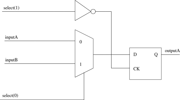
FIGURE 4.32. Diagram showing synthesized logic for module “case_infer.”
Example 4.57 Verilog Code Utilizing “default” Condition for “case” Statement

Figure 4.33 shows a diagram of the synthesized logic module “case_uninfer_diff.” Notice that the synthesized logic no longer has a latch.
FIGURE 4.33. Diagram showing synthesized logic for module “case_uninfer_diff.”
Apart from using the “default” condition as shown in the Verilog code of module “case_uninfer_diff” inference of a latch can also be avoided by specifing all the possible conditions of “select”
Example 4.58 Verilog Code Using “case” Statement with All Conditions Specified

Module “case_uninfer” of Example 4.58 and module “case_uninfer_diff” of Example 4.57 both synthesizes to the same logic and has the same functionality.
The Verilog code shown in Examples 4.56, 4.57, and 4.58 uses the “case” statement to obtain multiplexer functionality within an “always” block. The same functionality can be obtained by using a conditional operator.
Example 4.59 Verilog Code to Obtain Multiplexer Functionality Using Conditional Operator
module case_uninfer_assign (inputA, inputB, select, outputA);

input inputA, inputB ;
input [1:0] select;
output outputA;

wire outputA;

assign outputA = select[1] ? 1'b0 : select[0] ? inputB : inputA;

endmodule
4.10 MEMORY ARRAY
When coding in Verilog for synthesis, sometimes a designer may want to code a memory array. Coding a memory array is common in behavioral coding and synthesizable coding, but for synthesis, the memory array may be limited to only a small array.
In synthesis, when a one-bit memory cell is coded, it is synthesized to a multiplexer and a flip-flop. Representation of a one-bit memory cell with a multiplexer and a flip-flop is definitely a waste of silicon real estate. However, even though a memory cell is rather large in terms of die area, it is still common for a designer to code a memory array provided that the array is small. A good example would be when a designer needs a small set of registers to store certain values. Or a designer may also code a memory array for synthesis when designing a microcontroller or microprocessor that may need a small register file.
Figure 4.34 shows a diagram of a synthesized logic for a one-bit memory cell. Synthesizing a large array of memory cells is a waste of silicon area. However, synthesizing memory cells is rather simple when coding in synthesizable Verilog compared with schematic capturing of the same array.
Example 4.60 shows a Verilog code for a 1-kilobyte memory module that is synthesizable. However, the designer can take note that, although the Verilog code is simple and easy, synthesis of the code may take several minutes longer than it does on other simple Verilog code, because this short piece of code synthesizes to 1 kilobyte of memory.
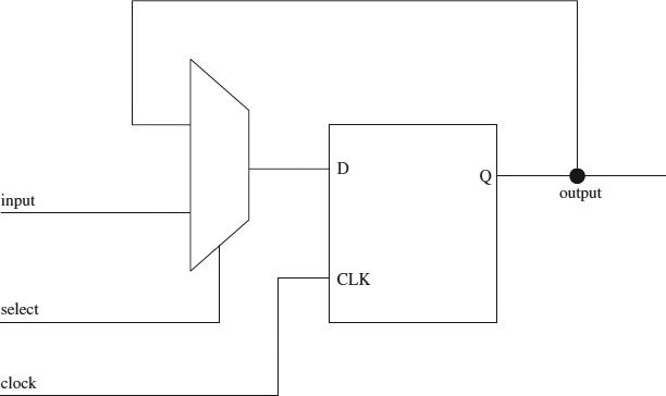
FIGURE 4.34. Diagram showing synthesis representation of a one-bit memory cell.
Example 4.60 Verilog Code for a 1-kilobyte Memory Array
module memory (addr, data_in, data_out, write, read, clock, reset);

// 1kbyte memory module - 128 address x 8 bits

input [6:0] addr;
input [7:0] data_in;
input write, read, clock, reset;
output [7:0] data_out;

reg [7:0] data_out;
reg [7:0] memory [127:0];

integer i;

// asynchronous reset
always @ (posedge clock or posedge reset)
begin
     if (reset)
          begin
              data_out = 0;
              // to initialize all memory to zero
              for (i=0; i<128; i=i+1)
               memory[i] <= 0;
          end
     else
          begin
               if (read)
                    data_out <= memory [addr];
               else if (write)
               begin
                        data_out <= 0;
                        memory [addr] <= data_in;
                   end
          end
end

endmodule
Example 4.61 shows a Verilog test bench that can be used to simulate the memory module shown in Example 4.60.
Example 4.61 Verilog Test Bench Module “memory_tb” to Simulate Module “memory”


Figure 4.35 is a diagram showing the waveform results of Verilog test bench module “memory_tb.”
Referring to Figure 4.35:
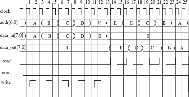
FIGURE 4.35. Diagram showing simulation waveform for Verilog test bench module “memory_tb”
- On rising edge of clock 1, 3, 5, 6, 8,10,11, and 13, read and write is at logical “0”. No reading or writing to memory occurs.
- On rising edge of clock 2, 4, 7, 9, and 12, write is at a logical “1”. A memory write occurs at address addr(6:0) with data data_in(7:0).
- On rising edge of clock 2, addr(6:0) = “A”, data_in(7:0) = “A”, write = ‘1’ → memory write at address “A” with data “A”.
- On rising edge of clock 4, addr(6:0) = “B”, data_in(7:0) = “B”, write = “1” → memory write at address “B” with data “B”.
- On rising edge of clock 7, addr(6:0) = “C”, data_in(7:0) = “C”, write = “1” → memory write at address “C” with data “C”.
- On rising edge of clock 9, addr(6:0) = “D”, data_in(7:0) = “D”, write = “1” → memory write at address “D” with data “D”.
- On rising edge of clock 12, addr(6:0) = “E”, data_in(7:0) = “E”, write = “1” → memory write at address “E” with data “E”.
- On rising edge of clock 15,16,18,20,21,23, and 25 read and write is at logical “0”. No reading or writing to memory occurs.
- On rising edge of clock 14,17,19, 22, and 24, read is at a logical “1”. A memory read occurs at address addr(6:0) and output data_out(7:0) is driven with data from the memory module.
- On rising edge of clock 14, addr(6:0) = “E”, read = “1” → memory read at address “E”. Data read is “E” and is shown on data_out(7:0).
- On rising edge of clock 17, addr(6:0) = “D”, read = “1” → memory read at address “D”. Data read is “D” and is shown on data_out(7:0).
- On rising edge of clock 19, addr(6:0) = “C”, read = “1” → memory read at address “C”. Data read is “C” and is shown on data_out(7:0).
- On rising edge of clock 22, addr(6:0) = “B”, read = “1” → memory read at address “B”. Data read is “B” and is shown on data_out(7:0).
- On rising edge of clock 24, addr(6:0) = “A”, read = “1” → memory read at address “A”. Data read is “A” and is shown on data_out(7:0).
4.11 STATE MACHINE DESIGN
A frequent design found in almost all types of digital design is a state machine. It is easy to design and gives the designer great flexibility when the designer needs to tweak the design either for speed or area optimization. Most synthesis tools in the market have special options to allow a designer to synthesize a state machine design. These options allow the designer to easily choose the form of state machine implementation, whether a binary encoding, gray encoding, or one hot encoding.
A state machine is always coded using a “case” statement. This statement allows for multiple conditions to be made for different decisions.
Designs that normally consist of a state machine are designs that have a fixed amount of known states, meaning that there is a fixed amount of states, with each state having its own functionality to perform.
Note: Most synthesis tools, such as Synopsys's Design Compiler, have special built-in algorithms for synthesizing state machine design (Synopsys's Design Compiler has a built-in Finite State Machine Compiler that is specially used for synthesizing and tweaking state machine). These special algorithm allow the designer to choose different types of encoding as well as different types of optimization to obtain the most optimal synthesis result, either in the form of area or performance. To have a better understanding of how Synopsys's Design Compiler (or rather Finite State Machine Compiler) can be used for optimizing state machine-based designs, please refer to VHDL Coding and Logic Synthesis with Synopsys, by Weng Fook Lee, published by Academic Press.
4.11.1 Intelligent Traffic Control System
A good example of a design that can be coded in state machine format is that of an intelligent traffic control system. A traffic control system has only certain fixed conditions to fulfill in order to control the traffic lights that control traffic flow.
Figure 4.36 shows an interchange junction of four roads. Traffic crossing the interchange junction needs to be regulated by a traffic light system in order to enable a smooth and safe interchange crossing for motorized vehicles. Now, assume that a design is needed to control the traffic light system.
FIGURE 4.36. Diagram showing an interchange junction traffic light.
Referring to Figure 4.36, the interchange junction has four sets of traffic lights, S1_S3, S2_S4, S1T_S3T, and S2T_S4T. These four sets of traffic lights allow four different passes on the interchange junction.
Figure 4.37 shows a possible scenario whereby the traffic lights of set S1_S3 are GREEN while all others are RED.
Figure 4.38 shows a possible second scenario whereby the traffic lights of set S2_S4 are GREEN while all others are RED.
Figure 4.39 shows a possible third scenario whereby the traffic lights of set S1T_S3T are GREEN while all others are RED.
Figure 4.40 shows a possible fourth scenario whereby the traffic lights of set S2T_S4T are GREEN while all others are RED.
Figures 4.37 through 4.40 show the possible passes through the interchange junction. Apart from the four sets of traffic lights of S1_S3, S2_S4, S1T_S3T, and S2T_S4T, there are present eight sensors, M1S, M1T, M2S, M2T, M3S, M3T, M4S, and M4T. Each sensor is strategically located in each road to sense whether there are any cars in queue. For example, if there are cars queuing to turn from road S2T or road S4T (as shown in Fig. 4.40), the sensor M2T would sense that cars are queuing at road S2T (or cars are queuing at road S4T, respectively). Similarly, the same for the other sensors. Sensors M1S would sense for cars queuing at road S1, M1T would sense for cars queuing at road S1T, sensor M2S would sense for cars queuing at road S2 and so forth. These eight sensors together with an external timer would allow for the building block of an “intelligent” traffic light system.
FIGURE 4.37. Diagram showing possible pass scenario whereby S1_S3 is GREEN.
FIGURE 4.38. Diagram showing possible pass scenario whereby S2_S4 is GREEN.

FIGURE 4.39. Diagram showing possible pass scenario whereby S1T_S3T is GREEN.
Based on the requirements stated, an interface block is created that defines the input and output signals of the traffic system controller. Figure 4.41 shows a figure of the input and outputs signals for the traffic light controller. Table 4.3 shows a description of the functions of each interface signal.
FIGURE 4.40. Diagram showing possible pass scenario whereby S2T_S4T is GREEN.

FIGURE 4.41. Diagram showing interface signals for traffic light controller.
TABLE 4.3. Interface Signal Description for Traffic Light Controller

Note: The inputs timerGreen, timerYellow, and timerRed are assumed to be generated from an external timer module that allows the traffic light controller to “know” that the allocated time period for the traffic lights at GREEN, YELLOW, or RED is exhausted and the traffic lights are to switch colors. It is also assumed that this timer module takes the inputs from the eight sensors to allow it to automatically determine if a certain traffic light should be at GREEN, YELLOW, or RED for a longer or shorter period of time before switching to another color.
Based on the interface signals as shown in Table 4.3 as well as the different conditions shown in Figures 4.37 through 4.40, a state diagram is drawn to reflect all the possible conditions or situations that may happen. The traffic light state machine controller must be able to handle all of the possible conditions. Figure 4.42 shows the state diagram for the traffic light state machine controller.
From Figure 4.42, each of the state transitions are represented by the following conditions:
A = timerRed=1 & (M3S=1 | M1S=1)
B = timerRed=1 & M1S=0 & M3S=0 & (M1T=1 | M3T=1)
C = timerRed=1 & M1S=0 & M3S=0 & M1T=0 & M3T=0 &
(M2S=1 | M4S=1)
D = timerRed=1 & M1S=0 & M3S=0 & M1T=0 & M3T=0 &
M2S = 0 & M4S = 0 & (M2T=1 | M4T=1)
E = timerRed=1 & (M1T=0 & M3T=0) &(M2S=0 & M4S=0) &
(M2T=1 | M4T=1)
F = timerRed=1 & (M1T=0 & M3T=0 & M2S=0 & M4S=0 &
M2T=0 & M4T=0 & (M1S=1 | M3S=1))
G = timerRed=1 & (M1T=0 & M3T=0) & (M2S=1 | M4S=1)
H = timerRed=1 & (M1T=1 | M3T=1)
I = timerRed=1 & M2S=0 & M4S=0 & M2T=0 & M4T=0 &
M1S = 0 & M3S = 0 & (M1T=1 | M3T=1)
J = timerRed=1 & M2S=0 & M4S=0 & M2T=0 & M4T=0 &
(M1S=1 | M3S=1)
K = timerRed=1 & (M2S=1 | M4S=1)
L = timerRed=1 & M2S=0 & M4S=0 & (M2T=1 | M4T=1)
M = timerRed=1 & (M2T=1 | M4T=1)
N = timerRed=1 & M2T=0 & M4T=0 & (M1S=1 | M3S=1)
P = timerRed=1 & M2T=0 & M4T=0 & M1S=0 & M3S=0 &
(M1T=1 | M3T=1)
Q = timerRed=1 & M2T=0 & M4T=0 & M1S=0 & M3S=0 &
M1T=0 & M3T=0 & (M2S = 1 | M4S = 1)

FIGURE 4.42. State diagram for traffic light state machine controller.
Referring to Figure 4.42:
- STATE1, STATE4, STATE7, STATE10 – all traffic lights are RED.
- In STATE1, there are four possible state transitions:
- State transition A occurs when timerRed is at logic “1” AND either sensor M1S OR M3S is at logic “1” (timerRed=1 & (M3S=1 | M1S=1)). This means that state transition A occurs when the allocated period for the traffic lights at RED is exhausted and there are cars queuing either at road S1 or S3.
- State transition B occurs when timerRed is at logic “1” AND sensor M1S, M2S is at logical “0” AND either sensor M1T OR M3T is at logic “1” (timerRed=1 & M1S=0 & M3S=0 & (M1T=1 | M3T=1). This means that state transition B occurs when the allocated period for the traffic lights at RED is exhausted and there are cars queuing either at road S1T or S3T and there are no cars queuing at road S1 and S3.
- State transition C occurs when timerRed is at logic “1” AND sensor M1S, M3S, M1T, M3T is at logical “0” AND either sensor M2S or M4S at logic “1” (timerRed=1 & M1S=0 & M3S=0 & M1T=0 & M3T=0 & (M2S=1 | M4S=1)). This means that state transition C occurs when the allocated period for the traffic lights at RED is exhausted and there are cars queuing either at road S2 or S4 and there are no cars queuing at road S1, S3, S1T, and S3T.
- State transition D occurs when timerRed is at logic “1” AND sensors M1S, M3S, M1T, M3T, M2S, and M4S are at logic “0” AND either sensor M2T OR M4T is at logic “1” (timerRed=1 & M1S=0 & M3S=0 & M1T=0 & M3T=0 & M2S=0 & M4S=0 & (M2T=1 | M4T=1)). This means that state transition D occurs when the allocated period for the traffic lights at RED is exhausted and there are cars queuing either at road S2T or S4T and there are no cars queuing at road S1, S3, S1T, S3T, S2, and S4.
- In STATE2, the traffic lights on road S1 and road S3 are GREEN. STATE2 will transition to STATE3 when timerGreen is at logical “1” (the allocated period for the traffic lights at GREEN is exhausted).
- In STATE3, the traffic lights on road S1 and road S3 is YELLOW. STATE3 will transition to STATE4 when timerYellow is at logical “1” (the allocated period for the traffic lights at YELLOW is exhausted).
- In STATE4, there are four possible state transitions.
- State transition E occurs when timerRed is at logic “1” AND sensor M1T, M3T, M2S, M4S is at logic “0” AND either sensor M2T OR M4T is at logic “1” (timerRed=1 & (M1T=0 & M3T=0) & (M2S=0 & M4S=0) & (M2T=1 | M4T=1)). This means that state transition E occurs when the allocated period for the traffic lights at RED is exhausted and there are cars queuing either at road S2T or road S4T and there are no cars queuing at road S1T, S3T, S2, and S4.
- State transition F occurs when timerRed is at logic “1” AND sensor M1T, M3T, M2S, M4S, M2T, and M4T is at logic “0” AND either sensor M1S OR M3S is at logic “1” (timerRed=1 & (M1T=0 & M3T=0 & M2S=0 & M4S=0 & M2T=0 & M4T=0 & (M1S=1 | M3S=1)). This means that state transition F occurs when the allocated period for the traffic lights at RED is exhausted and there are cars queuing either at road S1 or road S3 and there are no cars queuing at road S1T, S3T, S2, S4, S2T, and S4T.
- State transition G occurs when timerRed is at logic “1” AND sensor M1T and M3T is at logic “0” AND either sensor M2S OR M4S is at logic “1” (timerRed=1 & (M1T=0 & M3T=0) & (M2S=1 | M4S=1)). This means that state transition G occurs when the allocated period for the traffic lights at RED is exhausted and there are cars queuing either at road S2 or road S4 and there are no cars queuing at road S1T and S3T.
- State transition H occurs when timerRed is at logic “1” AND either sensor M1T OR M3T is at logic “1” (timerRed=1 & (M1T=1 | M3T=1)). This means that state transition H occurs when the allocated period for the traffic lights at RED is exhausted and there are cars queuing at road S1T or road S3T.
- In STATE5, the traffic lights on road S1T and road S3T are GREEN. STATE5 will transition to STATE6 when timerGreen is at logical “1” (the allocated period for the traffic lights at GREEN is exhausted).
- In STATE6, the traffic lights on road S1T and road S3T is YELLOW. STATE6 will transition to STATE7 when timerYellow is at logical “1” (the allocated period for the traffic lights at YELLOW is exhausted).
- In STATE7, there are four possible state transitions.
- State transition I occurs when timerRed is at logic “1” AND sensor M2S, M4S, M2T, M4T, M1S, and M3S is at logic “0” AND either sensor M1T OR M3T is at logic “1” (timerRed=1 & M2S=0 & M4S=0 & M2T=0 & M4T=0 & M1S=0 & M3S=0 & (M1T=1 | M3T=1)). This means that state transition I occurs when the allocated period for the traffic lights at RED is exhausted and there are cars queuing at road S1T or road S3T and there are no cars queuing at road S2, S4, S2T, S4T, S1, and S3.
- State transition J occurs when timerRed is at logic “1” AND sensor M2S, M4S, M2T and M4T is at logic “0” AND either sensor M1S OR M2S is at logic “1” (timerRed=1 & M2S=0 & M4S=0 & M2T=0 & M4T=0 & (M1S=1 | M3S=1)). This means that state transition J occurs when the allocated period for the traffic lights at RED is exhausted and there are cars queuing at road S1 or road S3 and there are no cars queuing at road S2, S4, S2T, and S4T.
- State transition K occurs when timerRed is at logic “1” AND either sensor M2S OR M4S is at logic “1” (timerRed=1 & (M2S=1 | M4S=1)). This means that state transition K occurs when the allocated period for the traffic lights at RED is exhausted and there are cars queuing at road S2 or road S4.
- State transition L occurs when timerRed is at logic “1” and sensor M2S and M4S is at logic “0” AND either sensor M2T OR M4T is at logic “1” (timerRed=1 & M2S=0 & M4S=0 & (M2T=1 | M4T=1)). This means that state transition L occurs when the allocated period for the traffic lights at RED is exhausted and there are cars queuing at road S2T or road S4T and there are no cars queuing at road S2 and S4.
- In STATE8, the traffic lights on road S2 and road S4 are GREEN. STATE8 will transition to STATE9 when timerGreen is at logical “1” (the allocated period for the traffic lights at GREEN is exhausted).
- In STATE9, the traffic lights on road S2 and road S4 is YELLOW. STATE9 will transition to STATE10 when timerYellow is at logical “1” (the allocated period for the traffic lights at YELLOW is exhausted).
- In STATE10, there are four possible state transitions:
- State transition M occurs when timerRed is at logic “1” AND either sensor M2T OR M4T is at logic “1” (timerRed=1 & (M2T=1 | M4T=1)). This means that state transition M occurs when the allocated period for the traffic lights at RED is exhausted and there are cars queuing at road S2T or road S4T.
- State transition N occurs when timerRed is at logic “1” AND sensor M2T and M4T is at logic “0” AND either sensor M1S OR M3S is at logic “1” (timerRed=1 & M2T=0 & M4T=0 & (M1S=1 | M3S=1)). This means that state transition N occurs when the allocated period for the traffic lights at RED is exhausted and there are cars queuing at road S1 or road S3 and there are no cars queuing at road S2T and road S4T.
- State transition P occurs when timerRed is at logic “1” AND sensor M2T, M4T, M1S, and M3S are at logic “0” AND either sensor M1T OR M3T is at logic “1” (timerRed=1 & M2T=0 & M4T=0 & M1S=0 & M3S=0 & (M1T=1 | M3T=1)). This means that state transition P occurs when the allocated period for the traffic lights at RED is exhausted and there are cars queuing at road S1T or road S3T and there are no cars queuing at road S2T, S4T, S1, and S3.
- State transition Q occurs when timerRed is at logic “1” AND sensor M2T, M4T, M1S, M3S, M1T, and M3T are at logic “0” AND either sensor M2S or M4S is at logic “1” (timerRed=1 & M2T=0 & M4T=0 & M1S=0 & M3S=0 & M1T=0 & M3T=0 & (M2S=1 | M4S=1)). This means that state transition Q occurs when the allocated period for the traffic lights at RED is exhausted and there are cars queuing at road S2 or road S4 and there are no cars queuing at road S2T, S4T, S1, S3, S1T, or S3T.
- In STATE11, the traffic lights on road S2T and road S4T are GREEN. STATE11 will transition to STATE12 when timerGreen is at logical “1” (the allocated period for the traffic lights at GREEN is exhausted).
- In STATE12, the traffic lights on road S2T and road S4T are YELLOW. STATE12 will transition to STATE1 when timerYellow is at logical “1” (the allocated period for the traffic lights at YELLOW is exhausted).
Based on the state diagram shown in Figure 4.42 and the interface pins shown in Figure 4.41 and described in Table 4.3, synthesizable Verilog code is written. Example 4.62 shows the Verilog code.
Example 4.62 Synthesizable Verilog Code for Traffic Light State Machine Controller
module state_machine (timerGreen, timerYellow,
timerRed, M1S, M2S, M3S, M4S, M1T, M2T, M3T, M4T,
clock, reset, S1_S3, S2_S4, S1T_S3T, S2T_S4T);

input timerGreen, timerYellow, timerRed, M1S, M2S,
M3S, M4S;
input M1T, M2T, M3T, M4T;
input clock, reset;
parameter [1:0] GREEN = 1,
                YELLOW = 2,
                RED = 3;

output [1:0] S1_S3, S2_S4, S1T_S3T, S2T_S4T;

parameter [3:0] STATE1 = 1,
                STATE2 = 2,
        STATE3 = 3,
        STATE4 = 4,
        STATE5 = 5,
        STATE6 = 6,
        STATE7 = 7,
        STATE8 = 8,
        STATE9 = 9,
        STATE10 = 10
        STATE11 = 11
        STATE12 = 12

reg [3:0] present_state, next_state;

always @ (timerGreen or timerYellow or timerRed or M1S
or M2S or M3S or M4S or M1T or M2T or M3T or M4T)
begin

        case (present_state)
        STATE1:
                begin
                    if (timerRed & (M3S | M1S))
               next_state = STATE2;
            else if (timerRed & ∼M1S & ∼M3S &
            (M1T | M3T))
                next_state = STATE5;
            else if (timerRed & ∼M1S & ∼M3S &
            ∼M1T & ∼M3T & (M2S | M4S))
                next_state = STATE8;
            else if (timerRed & ∼M1S & ∼M3S &
            ∼M1T & ∼M3T & ∼M2S & ∼M4S & (M2T
            | M4T)) next_state = STATE11;
            else
                        next_state = STATE1;
               end
           STATE2:
               begin
           if (timerGreen)
                  next_state = STATE3;
else
                   next_state = STATE2;
            end
        STATE3:
            begin
                if (timerYellow)
                   next_state = STATE4;
                else
                    next state = STATE3;
             end
        STATE4:
             begin
                 if (timerRed & ∼M1T & ∼M3T & ∼M2S
         & ∼M4S & (M2T | M4T))
                     next_state = STATE11;
         else if (timerRed & ∼M1T & ∼M3T &
         ∼M2S & ∼M4S & ∼M2T & ∼M3T & (M1S |
         M3S)) next_state = STATE2;
         else if (timerRed & ∼M1T & ∼M3T &
         (M2S | M4S))
                     next_state = STATE8;
         else if (timerRed & (M1T | M3T))
             next_state = STATE5;
                 else
                     next state = STATE4;
              end
          STATE5:
              begin
                  if (timerGreen)
                     next_state = STATE6;
                  else
                     next state = STATE5;
          end
              STATE6:
                  begin
                      if  (timerYellow)
                          next_state = STATE7;
              else
                          next_state = STATE6;
                   end
           STATE7:
                   begin
                       if (timerRed & ∼M2S & ∼M4S & ∼M2T
               & ∼M4T & ∼M1S & ∼M3S & (M1T |
               M3T)) next_state = STATE5;
else if (timerRed & ∼M2S & ∼M4S &
                   ∼M2T & ∼M4T & (M1S | M3S))
                    next_state = STATE2;
            else if (timerRed & (M2S | M4S))
                next_state = STATE8;
            else if (timerRed & ∼M2S & ∼M4S &
                (M2T | M4T))
                next_state = STATE11;
            else
                next_state = STATE7;
            end
                    STATE8:
                        begin
                if (timerGreen)
                               next_state = STATE9;
                           else
                   next_state = STATE8;
                           end
                       STATE9:
                           begin
                               if (timerYellow)
                       next_state = STATE10;
                   else
                       next_state = STATE9;
                            end
                       STATE10:
                           begin
                               if (timerRed & (M2T | M4T))
                      next_state = STATE11;
                   else if (timerRed & ∼M2T & ∼M4T &
                       (M1S | M3S))
                   next_state = STATE2;
                   else if (timerRed & ∼M2T & ∼M4T &
                       ∼M1S & ∼M3S & (M1T | M3T))
                       next_state = STATE5;
                   else if (timerRed & ∼M2T & ∼M4T &
                   ∼M1S & ∼M3S & ∼M1T & ∼M3T &
                  (M2S | M4S)) next_state = STATE8;
                  else
                      next_state = STATE10;
                          end
                     STATE11:
                 begin
                             if (timerGreen)
                    next state = STATE12;
else
                    next_state = STATE11;
                         end
            STATE12:
                begin
                            if (timerYellow)
                               next_state = STATE1;
                           else
                               next_state = STATE12;
               end
                  default:
              next_state = STATE1;
              endcase
end

// creation of state flops

always @ (posedge clock or posedge reset)
begin
        if (reset)
            present_state <= STATE1;
        else
                present_state <= next_state;
end

// assignment of output signals

assign S1_S3 = (present_state == STATE2) ? GREEN :
(present_state == STATE3) ? YELLOW : RED;

assign S1T_S3T = (present_state == STATE5) ? GREEN :
(present_state == STATE6) ? YELLOW : RED;

assign S2_S4 = (present_state == STATE8) ? GREEN :
(present_state == STATE9) ? YELLOW : RED;

assign S2T_S4T = (present_state == STATE11) ? GREEN :
(present_state == STATE12) ? YELLOW : RED;

endmodule
With the synthesizable Verilog code as shown in Example 4.62, a Verilog test bench is written to simulate the design module state_machine.
Example 4.63 Verilog Test Bench to Simulate Design Module state_machine


FIGURE 4.43. Diagram showing simulation results of test bench module state_machine_tb.
Note: The Verilog test bench is written to show the reader how a test bench can be written to simulate the design module state_machine. It can always be written in some other manner that can achieve the same objective. Also take note that the test bench only simulates a small portion of the conditions of the traffic light state machine controller.
Figure 4.43 shows the simulation waveform result of the test bench state_machine_tb.