
CHAPTER FIVE
Design Example of Programmable Timer
Chapter 3 explained the basic concept of Verilog, and Chapter 4 showed some common known coding methods that are used in synthesis. Chapter 5 shows an example of how a real-life practical design can be achieved, beginning from design specification, architectural definition, coding, and verification.
The example discussed in Chapter 5 is a design of a programmable timer. Timers are common design modules in almost all types of system. The design of the programmable timer begins with a design specification for its features and capabilities.
5.1 PROGRAMMABLE TIMER DESIGN SPECIFICATION
The programmable timer is an eight-bit timer that allows three different modes, a one-shot timer, a pulse generator, and a 50% duty cycle waveform generator. For each mode, a certain value can be loaded into the timer before the timer begins clocking. The timer can determine which mode to operate in by using an internal register. This internal register is referred to as “control word register.” The control word register is a three-bit register with the MSB bit representing “timer enable” and bit 1 and bit 0 represents the mode of operation.
Referring to Figure 5.1:
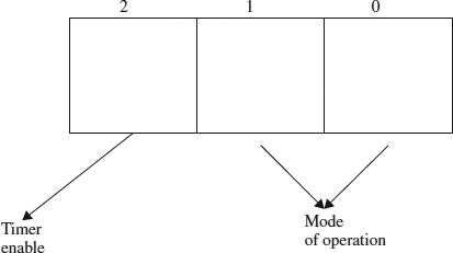
FIGURE 5.1. Diagram showing bits of control word register.
- Timer enable—this bit if set to a “1” would enable the timer.
- Mode of operation:
- Mode “00”—one-shot timer. In this mode, the timer is loaded with an eight-bit binary value. A three-bit value of “100” (timer enable and operate in mode 0) is written into the control word register of the timer. The timer then begins to count up through each rising edge of clock. When the timer reaches a hex value of “FF”, the output of the timer generates a one-clock-width pulse. The timer would then overwrite its MSB of the control word register to a “0” and the timer would stop. To continue the one-shot timer, the MSB of the control word register would need to be rewritten to a value of “1”.
- Mode “01”—pulse generator. In this pulse generator mode, the timer is loaded with an eight-bit binary value. A three-bit value of “101” (timer enable and operation in mode 1) is written into the control word register of the timer. The timer then begins to count up through each rising edge of clock. When the timer reaches a hex value of “FF”, the output of the timer would generate a one-clock-width pulse. The timer is then automatically reloaded again with the initial value that was loaded into the timer and the count begins again. Unlike mode 0, the MSB of the control word register is not overwritten with a “0”. The timer in this mode does not stop unless the user writes a “0” to the MSB of the control word register or if ceb is pulled to a logic “1”.
- Mode “10”—50% duty cycle waveform generator. In this waveform generator mode, the timer is loaded with an eight-bit binary value. A three-bit value of “110” (timer enable and operation in mode 2) is written into the control word register of the timer. Unlike mode 0 or 1, the timer would count down and not count up. When the timer reaches a hex value that is half of the loaded value, the output of the timer would generate a logic “1”. The timer continues to count down and when it reaches a hexadecimal value of “00”, the timer would be reloaded automatically with the initial loaded value and count down again. Similar to mode 1, the timer in this mode does not stop unless the user writes a “0” to the MSB of the control word register or if ceb is pulled to a logic “1”.
In mode 2 of operation, the output of the timer would oscillate between 0 and 1 whenever the timer reaches half of the value loaded into the timer. This would create a waveform generator that has 50% duty cycle.
- Mode “11”—not used.
Apart from the control word register, the programmable timer has an eightbit latch and an eight-bit counter. The eight-bit latch allows a user to latch in a certain binary value. This value is then loaded into the eight-bit counter when the programmable timer is enabled.
With these requirements in mind, an interface specification is defined for the input and output signals.
Table 5.1 shows the signal description for each of the input and output port for the programmable timer design as shown in Figure 5.2.
5.2 MICROARCHITECTURE DEFINITION FOR PROGRAMMABLE TIMER
Based on the design specification from Section 5.1, a microarchitecture can be derived for the design. The requirements of a control word register would point to the need of a three-bit register, with each bit being able to control the programmable timer. Because the programmable timer is eight bits wide, there must be an eight-bit counter that is able to count up or count down depending on the mode of execution. A decoder is also needed to decode the output of the eight-bit counter (depending on the mode of execution) to generate an output waveform for the programmable timer. Figure 5.3 shows a microarchitectural block diagram of the programmable timer design.
TABLE 5.1. Signal description for programmable timer design
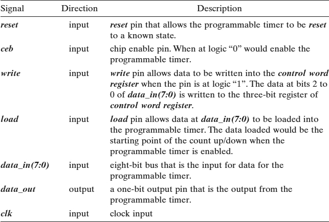

FIGURE 5.2. Diagram showing the interface signals for programmable timer design.
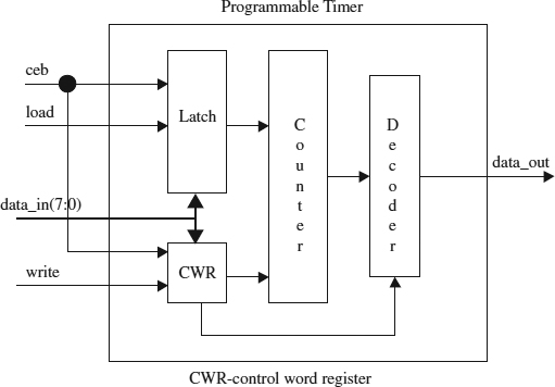
FIGURE 5.3. Microarchitectural block diagram of the programmable timer design.
Referring to Figure 5.3, the programmable timer microarchitecture is partitioned into four major portions:
- latch. This is an eight-bit latch to latch in the value that is loaded into the counter as the starting point for the counter to count up/down.
- CWR. This is the control word register, which is a three-bit register that determines if the counter is enabled and what mode to enable the counter in.
- counter. This is an eight-bit counter that counts up/down depending on which mode the programmable timer is operating in.
- decoder. This is a decoder that decodes the output of the counter to generate the output for the programmable timer.
5.3 FLOW DIAGRAM DEFINITION FOR PROGRAMMABLE TIMER
Before synthesizable Verilog code is written for the programmable timer, a designer should always spend some time drawing a flow diagram to represent the process flow of the design. Such a diagram can be very useful when the designer starts to write the Verilog code for the design.
The designer does not need to restrict himself/herself to only using flow diagrams. The designer can choose to draw state diagrams, bubble diagrams, or even pseudocode, depending on which is more suitable.
Figure 5.4 shows a flow diagram that covers the conditions that the user can use to load binary data into the programmable timer or writing data into the control word register.
Referring to Figure 5.4:
- When ceb and load are at logic “0” while write is at logic “1”, the data from data_in bits 2 to 0 are written into the control word register.
FIGURE 5.4. Flow diagram for loading data into programmable timer and writing data into control word register.
- When ceb and write are at logic “0” while load is at logic “1”, the data from data_in are written into latch_counter. This is an eight-bit register in the programmable timer that is used to store the value that is loaded into the counter. The counter in the programmable timer will count up or down (depending on mode of operation) using this value in the latch_counter as the starting count. Furthermore, in mode 1 and mode 2 operation of the programmable timer, automatic reload of the counter is required. Therefore, some form of storage is required for the initial data.
- When ceb is at logic “1”, latch_counter and control word register are reset.

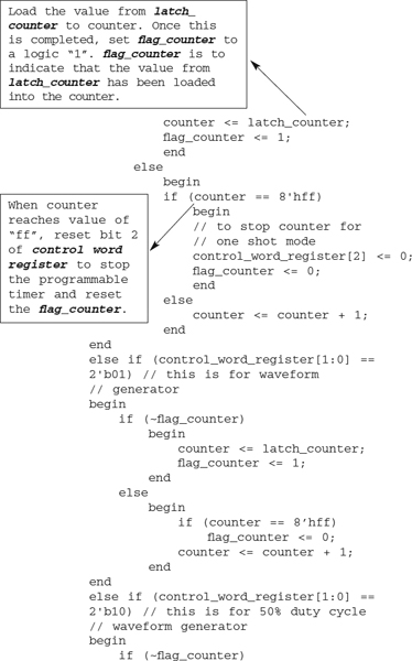
Figure 5.5 shows the flow diagram for resetting the programmable timer when a rising edge is detected at the reset signal. Notice that during reset, the variables flag_counter, counter, and flag_half_counter are reset. These variables are flags used in the design of the programmable timer for different modes that it is able to operate in. How these variable are used is shown in the flow diagrams in Figures 5.6, 5.7, and 5.8.
Referring to Figure 5.6:
- At positive edge of clk, bit 2 of control word register is checked for a logic value of “1” (logic value “1” on bit 2 indicates the programmable timer is enabled). If it is, then bit 1 and 0 of control word register is checked for a value of “00” (bits 1 and 0 indicates the mode of operation for the programmable timer). If it is, a flag called flag_counter is checked for a logic value of “0” (flag_counter is used to indicate that the value in the latch_counter register is loaded into the counter). If it is, the value in the latch_counter registers are loaded into the counter and the flag_counter is set to a logic “1”.
FIGURE 5.5. Flow diagram for reset of programmable timer.
FIGURE 5.6. Flow diagram for mode 0 operation.
- If control word register is detected at a value of “100” and flag_counter is at logic “1”, the counter is checked for a value of “ff”. If it is, then bit 2 of control word register is reset and flag_counter is also reset. If the counter is at a value other than “ff”, the counter is incremented by 1.

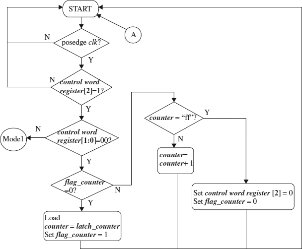
Figure 5.7 shows a flow diagram (continue from flow diagram of Figure 5.6) for programmable timer at mode 1 execution.
Referring to Figure 5.7:
- From the connecter for Mode1 from Figure 5.6, bits 1 and 0 of control word register are checked for logic value of “01” (bits 1 and 0 indicate the mode of operation for the programmable timer). If the logic value is “01”, a flag called flag_counter is checked for a logic value of “0” (flag_counter is used to indicate that the value in the latch_counter register is loaded into the counter). If it is, the value in the latch_counter registers are loaded into the counter and flag_counter is set to a logic “1”.
FIGURE 5.7. Flow diagram for mode 1 operation.
- If control word register is detected at a value of “101” and flag_counter is at logic “1”, the counter is checked for a value of “ff”. If it is, flag_counter is reset. The counter would then be incremented by 1. If the counter has a value other than “ff”, the counter is incremented by 1.

Figure 5.8 shows a flow diagram (continue from flow diagram of Figure 5.7) for a programmable timer at mode 2 execution.
Referring to Figure 5.8:

FIGURE 5.8. Flow diagram for mode 2 operation.
- From the connecter for mode 2 from Figure 5.7, bits 1 and 0 of control word register are checked for a logic value of “10” (bits 1 and 0 indicate the mode of operation for the programmable timer). If the logic value is “10”, a flag called flag_counter is checked for a logic value of “0” (the flag_counter is used to indicate that the value in the latch_counter register has been loaded into the counter). If it is, the value in the latch_counter registers is loaded into the counter and flag_counter is set to logic “1”.
- If control word register is detected at a value of “110” and flag_counter is at logic “1”, the counter is checked for a value that is half of the value stored in latch_counter. If it is, flag_half_counter is set to the inverse of its previous value. The counter would then be decremented by 1. If the counter has a value other than half of the value stored in latch_counter, the counter is then checked for a value of 0. If it is not 0, then the counter would be decremented by 1. However if the counter is at a value of 0, then flag_counter is reset.
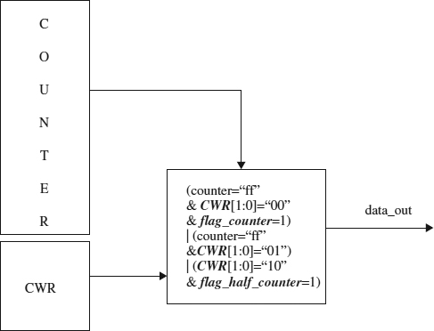
FIGURE 5.9. Diagram showing decoding of control word register and counter for output generation.
The flow diagrams in Figures 5.6, 5.7, and 5.8 show three different flow diagrams that allow the programmable timer to execute its three different modes. Figure 5.9 shows the conditions of decodings of the counter to create the necessary output for the programmable timer.
Referring to Figure 5.9, decoding to obtain the output data_out as a logic “1” occurs:
- a. when the counter reaches a value of “ff” and bits 1 and 0 of control word register are decoded as “00” and flag_counter is “1”;
- b. when the counter reaches a value of “ff” and bits 1 and 0 of control word register are decoded as “01”;
- c. when the control word register is decoded as “10” and flag_half_counter is decoded as “1”.
Note: Decoding to generate the output data_out uses signal flag_counter only when the programmable timer is in mode 0 execution. During mode 0 execution (one-shot mode), the programmable timer only creates one pulse and then is disabled. For this reason, the data_out is decoded with flag_counter, which is reset to logic “0” when the counter reaches a value of “ff”.
5.4 VERILOG CODE FOR PROGRAMMABLE TIMER
Based on the specifications and flow diagrams shown in Sections 5.1, 5.2 and 5.3, Verilog code is written for the programmable timer (as shown in Example 5.1).
Note: The Verilog code shown in Example 5.1 is not entirely synthesizable. However, the code shown is a simulation that will give the correct results with reference to the requirements of the programmable timer based on the specification in Section 5.1, the microarchitecture definition in Section 5.2, and the flow diagrams in Section 5.3. What this example is trying to point out is that designers need to be careful when writing Verilog code (or VHDL code) for synthesis. Very often, inexperienced designers write code that would simulate to give the right simulation results but would synthesize to some garbage circuits or, even worse, would not synthesize at all. Example 5.1 is one such example. It is a piece of Verilog code that looks correct and simulates correctly but will not synthesize. Why Example 5.1 is not synthesizable is discussed in detail in Section 5.5. Can you detect which part of the code in Example 5.1 is causing the code to be nonsynthesizable? For the time being, let's assume that the code in Example 5.1 is synthesizable.
Example 5.1 Verilog Code for Programmable Timer


Example 5.2 shows a test bench that is used to simulate the Verilog code of the programmable timer executing in mode 0.
Example 5.2 Verilog Test Bench to Simulate Programmable Timer Executing in Mode 0
![]()
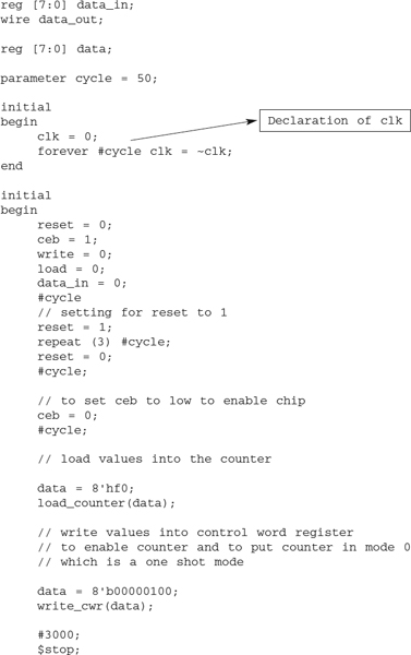

Figure 5.10 shows the simulation waveform for the Verilog test bench used to simulate the programmable timer at mode 0 execution.
Referring to Figure 5.10:
- In clock 1 and clock 2, reset signal is at logic “1”. This resets the counter, flag_counter, and flag_half_counter.
- In clock 3, ceb goes to logic “0” to enable the programmable timer.
- In clock 4, load signal is at logic “1”. This would load the value “f0” at the data_in bus to the latch_counter.
- In clock 5, write signal is at logic “1”. This will write the value “4” at the data_in bus to the control word register.
- In clock 6, write and load is at logic “0”, while control word register is at a value of “100”. Bits 1 and 0 decode the operation of programmable timer in mode 0. Bit 2 decodes the enabling of the programmable timer.Therefore, at clock 6, the value of latch_counter is loaded into the counter, thereby having the counter at a value of “f0”. During clock 6, the signal flag_counter is driven to logic “1”.
FIGURE 5.10. Diagram showing simulation results of Verilog test bench for mode 0.
- From clock 7 to clock 20, the counter would increment by 1 during every rising edge of clock.
- In clock 21, the counter reaches a value of “ff”. This is decoded to create an output on data_out with a logic “1”.
- In clock 22, bit 2 of control word register is reset to a logic “0”. This would disable the programmable timer. At the same time flag_counter is also reset.

Note: The signal flag_counter is created as a flag to signify that the counter has already been loaded with the value from the latch_counter. This flag is then used together with the counter value and control word register bits 1 and 0 to decode for the output data_out.
Also, note that in mode 0, the programmable timer functions as a one-shot device. Once the output data_out drives a pulse, it would then stop. The programmable timer will need to be enabled again by writing a command to the control word register to enable the programmable timer.
Example 5.3 shows a test bench that is used to simulate the Verilog code of the programmable timer executing in mode 1.
Example 5.3 Verilog Test Bench to Simulate Programmable Timer Executing in Mode 1
module prog_counter_tb ();

reg reset, ceb, write, clk, load;
reg [7:0] data_in;
wire data_out;

reg [7:0] data;

parameter cycle = 50;

initial
begin
     clk = 0;
     forever #cycle clk = ~clk;
end

initial
begin
     reset = 0;
     ceb = 1;
     write = 0;
     load = 0;
     data_in = 0;
     #cycle
     // setting for reset to 1
     reset = 1;
     repeat (3) #cycle;
     reset = 0;
     #cycle;

     // to set ceb to low to enable chip
     ceb = 0;
     #cycle;

     // load values into the counter

     data = 8'hfa;
     load_counter(data);
// write values into control word register
     // to enable counter and to put counter in mode 1
     // which is a pulse waveform generator

     data = 8'b00000101;
     write_cwr(data);

     #3000;
     $stop;
end

task write_cwr;
input [7:0] data;
begin
     write = 1;
     data_in = data;
     repeat (2) #cycle;
     write = 0;
     data_in = 0;
     #cycle;
end
endtask

task load_counter;
input [7:0] data;
begin
     load = 1;
     data_in = data;
     repeat (2) #cycle;
     load = 0;
     data_in = 0;
     #cycle;
end
endtask

prog_counter prog_counter_inst (reset, ceb, write,
data_in, clk, load, data_out);

endmodule
Figure 5.11 shows the simulation waveform for the Verilog test bench used to simulate the programmable timer at mode 1 execution.
Referring to Figure 5.11:
- In clock 1 and clock 2, reset signal is at logic “1”. This resets the counter, flag_counter, and flag_half_counter.
FIGURE 5.11. Diagram showing simulation results of Verilog test bench for mode 1.
- In clock 3, ceb goes to logic “0” to enable the programmable timer.
- In clock 4, load signal is at logic “1”. This would load the value “fa” at the data_in bus to the latch_counter.
- In clock 5, write signal is at logic “1”. This will write the value “5” at the data_in bus to the control word register.
- In clock 6, write and load is at logic “0”, while control word register is at a value of “101”. Bits 1 and 0 decode the operation of the programmable timer in mode 1. Bit 2 decodes to enabling of programmable timer. At clock 6, the value of latch_counter is loaded into the counter, thereby having the counter at a value of “fa”. During clock 6, the signal flag_counter is driven to logic “1”.
- From clock 7 to clock 11, the counter would increment by 1 during every rising edge of clock.
- At clock 11, the counter reaches the value of “ff”. This counter value is decoded to create the output data_out to be at logic “1”. During this clock, the signal flag_counter is reset to 0. However, the flag_counter does not go to a logic “0” immediately in clock 11, but instead would go to a logic “0” in clock 12. This occurs because in clock 11, when the counter is at the value of “ff”, the flag_counter is assigned the value of logic “0”. And this assignment will take place on the next clock (the signal is flopped).
- Clock 12 have the flag_counter at a logic value of “0”.
- In clock 13, the counter is automatically reloaded with the value “fa” in the latch_counter. Signal flag_counter is at logic value of “1” and the steps from clock 7 is repeated. This will continue until:
- a. a reset happens
- b. ceb goes back to logic “1”
- c. a new value is written into the control word register

Note: For mode 1 of operation, the timer automatically reloads the counter everytime flag_counter switches from logic “0” to logic “1”. Therefore, the output waveform at data_out is a pulse generator.
Example 5.4 shows a test bench that is used to simulate the Verilog code of the programmable timer executing in mode 2.
Example 5.4 Verilog Test Bench to Simulate Programmable Timer Executing in Mode 2
module prog_counter_tb ();

reg reset, ceb, write, clk, load;
reg [7:0] data_in;
wire data_out;

reg [7:0] data;

parameter cycle = 50;

initial
begin
     clk = 0;
     forever #cycle clk = ~clk;
end

initial
begin
     reset = 0;
     ceb = 1;
     write = 0;
     load = 0;
     data_in = 0;
     #cycle
// setting for reset to 1
     reset = 1;
     repeat (3) #cycle;
     reset = 0;
     #cycle;

     // to set ceb to low to enable chip
     ceb = 0;
     #cycle;

     // load values into the counter

     data = 8'h05;
     load_counter(data);

     // write values into control word register
     // to enable counter and to put counter in mode 2
     // which is a 50% duty cycle waveform generator

     data = 8'b00000110;
     write_cwr(data);

     #3000;
     $stop;
end

task write_cwr;
input [7:0] data;
begin
     write = 1;
     data_in = data;
     repeat (2) #cycle;
     write = 0;
     data_in = 0;
     #cycle;
end
endtask

task load_counter;
input [7:0] data;
begin
     load = 1;
     data_in = data;
     repeat (2) #cycle;
     load = 0;
data_in = 0;
     #cycle;
end
endtask

prog_counter prog_counter_inst (reset, ceb, write,
data_in, clk, load, data_out);

endmodule
Figure 5.12 shows the simulation waveform for the Verilog test bench used to simulate the programmable timer at mode 2 execution.
Referring to Figure 5.12:
- In clock 1 and clock 2, reset signal is at logic “1”. This resets the counter, flag_counter, and flag_half_counter.
- In clock 3, ceb goes to logic “0” to enable the programmable timer.
- In clock 4, load signal is at logic “1”. This would load the value “5” at the data_in bus to the latch_counter.
- In clock 5, write signal is at logic “1”. This will write the value “6” at the data_in bus to the control word register.
- In clock 6, write and load is at logic “0”, while control word register is at a value of “110”. Bits 1 and 0 decode the operation of programmable timer in mode 2. Bit 2 decodes the enabling of the programmable timer. At clock 6, the value of latch_counter is loaded into the counter, thereby having the counter at a value of “5”. During clock 6, the signal flag_counter is driven to logic “1” to indicate that the values in the latch_counter have been loaded into the counter.
FIGURE 5.12. Diagram showing simulation results of Verilog test bench for mode 2.
- From clock 7 to clock 11, the counter would decrement by 1 during every rising edge of clock.
- In clock 9, the counter reaches a value of “2”. Because the counter was initially loaded with the value 5, half of 5 is 2 (rounded from 2.5). Therefore in clock 9, the flag_half_counter is assigned to a logic value of “1”. This assignment value on flag_half_counter is not seen at clock 9 but only seen at clock 10. The reason for this is again because in clock 9, when the assignment of logic “1” to flag_half_counter occurs, the rising edge of clock 9 has already occurred. On the rising edge of clock 9, the counter is decremented by one to a value of “2”. The decoding of this value “2” for the counter causes the assignment of logic “1” to flag_half_counter, but the rising edge of clock 9 has already occurred. Therefore, flag_half_counter would only have the value of logic “1” on the rising edge of clock 10.
- At clock 11, the counter reaches the value of “00”. When this occurs, flag_counter is reset. Again, similarly as in clock 9, assignment of logic “0” to flag_counter is not seen until clock 12. This is due to the fact that when the counter is decremented to a value of “00” (during rising edge of clock 11), the decoding of this counter value causes the assignment of logic “0” to flag_counter. However, because it is no longer the rising edge of clock 11, the assignment of the value would occur on the rising edge of clock 12.
- At clock 13, flag_counter reset and the counter is reloaded with the value from latch_counter and the whole counting process repeats. However, note that in clock 16, when counter reaches the value of “2” (half of 5), flag_half_counter goes to logic “0” in clock 17. The design basically has flag_half_counter toggling between logic “1” and “0” every time the counter reaches half the value stored in latch_counter.
- Output data_out follows the waveform of flag_half_counter.

Note: Mode 2 of operation is similar to mode 1 of operation whereby the counter in the programmable timer is automatically reloaded when the counter reaches a value of “00”. This would create an output waveform data_out that is a 50% duty cycle waveform generator.
The synthesizable Verilog code shown in Example 5.1 for the programmable timer has the assignment statements flag_counter and flag_half_counter within the always statement that detects a rising edge of clock. This method of coding flops both the signals. As a result, assignment of values to the signal flag_counter and flag_half_counter always happens one clock later (because it is flopped). A designer should always note that when a signal is assigned a value within an always statement that detects for a rising edge or falling edge, that signal will be flopped.
5.5 SYNTHESIZABLE VERILOG CODE FOR PROGRAMMABLE TIMER
Based on the simulation waveform results shown in Figures 5.10, 5.11 and 5.12, the Verilog code of Example 5.1 gives the correct and expected simulation results. However, when the Verilog code is synthesized, an error will occur. Do you know where the error is?
Referring to the Verilog code in Example 5.1, there are two always statements. The first always statement is
always @ (ceb or write or reset or load)
begin
     if (~ceb & write & ~load & ~reset)
          control_word_register = data_in [2:0];
     else if (~ceb & ~write & load & ~reset)
          latch_counter = data_in;
     else if (ceb & ~reset)
          begin
               // reset the control word counter
           control_word_register = 0;
               // reset the latch_counter
           latch_counter = 0;
          end
end
which creates a set of latches for latch_counter and control_word register. This is the statement that sets the assignments for the signal control_word_register as well as latch_counter.
The second always statement is
always @ (posedge clk or posedge reset)
begin
     if (reset)
     begin
          flag_counter <= 0;
          counter <= 0;
          flag_half_counter <= 0;
     end
     else
     begin
if (control_word_register[2]) // counter is enabled
          begin
               if (control_word_register[1:0] == 2'b00)
               // this is
               // for one shot mode
               begin
                    if (~flag_counter)
                         begin
                         counter <= latch_counter;
                         flag_counter <= 1;
                         end
                    else
                         if (counter == 8'hff)
                            begin
                            // to stop counter for one shot
                            // mode
                            control_word_register[2] <= 0;
                            flag_counter <= 0;
                            end
                         else
…
…
…
             end
      end
end
which creates a set of flip-flops triggered by rising edge of clk for signals flag_counter, flag_half_counter, and counter. However, in this second always statement, during the execution of the programmable timer at mode 0, assignment of value to the control word register occurs to disable the timer when the one shot pulse has been generated by the timer:
control_word_register[2] <= 0;
This causes a conflicting problem in the sense that the first always statement drives a value on the control word register while the second always statement also drives a value on the control word register. During synthesis, the synthesis tool is confused and would not know which circuit to synthesize. There are multiple drivers on the node and the synthesis tool would not know which driver is allowed to drive the node (as contention occurs). If the design is coded in such a way as to create the control word register as a tri-state register, it is possible to have different circuits to drive a node. However, in this case, the control word register is a logic register that cannot have two separate circuits driving a node.
In synthesis, a synthesis tool would need to know the logic that is required to drive a node before being able to synthesize the necessary circuit to drive a node.
There are many ways to fix this problem. The Verilog code in Example 5.5 shows one method of coding to resolve this problem.
Example 5.5 Synthesizable Verilog Code for Programmable Timer

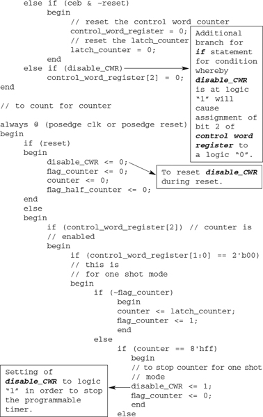

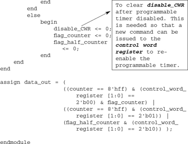
The Verilog code in Example 5.5 is different from Example 5.1 in that a new signal called disable_CWR is introduced. In Example 5.5, this signal is used to assign a logic “0” to the most significant bit of control word register. In other words, the signal disable_CWR acts as a qualifier signal for enabling or disabling the MSB of control word register. By so doing, the driver for control word register is limited to only the first always statement. And, therefore, there is no longer a situation in which contention may happen.
The Verilog code in Example 5.5 can be simulated using the same test bench in Example 5.2, 5.3, and 5.4. The simulation results are the same as that for the simulation of Verilog code for Example 5.1.
This comparison between Verilog code of Example 5.1 and 5.5 shows a very important difference between writing Verilog code for simulation and for synthesis. A piece of code that simulates correctly does not necessarily mean that it would synthesize. Therefore, it is important for a designer to understand the limitations of writing code for synthesizability.