
4.3 Issues Related to CMOS Scaling
4.4 Porphyrin SAMs as Copper Diffusion Barriers
4.4.1 Copper/Low-k Technologies in ULSI Metallization
4.4.2 Cu Diffusion Barriers in ULSI Metallezation
4.4.3 Porphyrin SAMs as Cu Diffusion Barriers in ULSI Metallization
4.4.3.1 Bias–Temperature–Stress Analysis
4.4.3.2 Secondary Ion Mass Spectrometry
4.5 Porphyrin SAMs For Metal Gate Work Function Tuning
4.5.1 Potential Gate Electrodes for Work Function Engineering
4.5.2 Porphyrin SAMs for Work Function Engineering
4.6.2 Electrical Transport Modification in RGO FETs Using Porphyrin SAMs
To date, feature sizes in complementary metal–oxide–semiconductor (CMOS) technologies have been scaled from 3 μm to sub-nanometers using the “top-down” scaling techniques [1]. In the sub-nanometers regime, miniaturization with the top-down techniques is not only becoming complex and expensive but also it is limited by the spatial resolution of lithography, variability, and longer fabrication turnaround times [2, 3 and 4]. To overcome these issues, “bottom-up” nanotechnologies or the combination of bottom-up and top-down fabrication methodologies can be used to fabricate devices [5, 6, 7 and 8]. This approach provides a way to fabricate devices with feature sizes smaller than 10 nm, three-dimensional complex nanostructures and to make devices with novel functionalities (Figure 4.1).
In the bottom-up self-assembly, self-assembled monolayers (SAMs) of molecules are used to build well-ordered structures with novel electronic, optical, and magnetic properties [9,10]. SAMs show the feasibility to change surface chemical and physical properties at the molecular level. Thus, they have been widely used for modifying the surface wetting/adhesion properties, sensor applications, corrosion resistance, and molecular electronics [11,12]. SAMs with atomic thickness and spacing are used as ultra-thin resists and passivating layers [13]. For example, SAMs of 1H,1H,2H,2H-perfluorodecyltrichlorosilane [CF3(CF2)7(CH2)2SiCl3, FDTS] have been used as release and antistiction coatings in MEMS (microelectromechanical systems) technology [14].
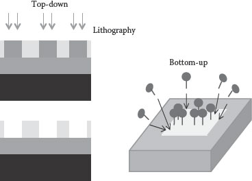
FIGURE 4.1 Top-down fabrication involving patterning, lithography, and etching versus bottom-up self-assembly process.
This chapter describes the potential applications of metalloporphyrin SAMs in nano-CMOS scaling and in modifying electronic properties of graphene field effect transistors (FETs). First, an introduction to the SAMs and the formation of SAMs are discussed followed by porphyrins and their applications in nanoelectronics. Later, a few issues related to CMOS scaling are discussed. In this chapter, the applications of porphyrin SAMs as copper diffusion barriers, for gate electrode work function tuning, and in modifying the electronic properties of graphene FETs have been discussed.
Self-assembly is the spontaneous organization of molecules into higher-ordered patterns or structures [15]. The molecules that form SAM are called surfactants, which comprising of a headgroup which adsorbs on the substrate, an end-group that constitutes the outer surface of the film, and a backbone that connects the head- and the end-group. The idea of SAMs was first explained by Sagiv et al. [16] who show that the adsorption from organic solutions on polar solid surfaces can be used to produce homogeneous, compact monolayers. It was observed that the adsorption is always limited to the completion of a single monolayer, which is adsorbed directly on the surface of the substrate. Monolayer systems with many technological applications are the structures of silanes on hydroxylated surfaces (siloxane chemistry). SAM preparation involves the use of alkylchlorosilanes, alkylalkoxysilanes, and alkylaminosilanes to form monolayers [17,18]. Besides silanes (R-SiX3, where X = Cl, OMe, OEt), organometallics (R-Li or R-MgX) and alcohols (R-OH) are also used for the formation of SAMs (where −R is the surface group). Self-assembly of silanes takes place through surface silanol groups (–SiOH) via Si–O–Si bonds. In this process, silanol groups on hydroxylated surfaces act as a support for monolayer formation or convert to highly reactive sites such as Si–Cl or Si–Br for SAM development. In case of surfaces activated with Si–Cl bonds, monolayer formation happens via Si–O or Si–N linkages when exposed to alcohol or amine molecules [19]. Figure 4.2 depicts the monolayer formation on oxide surfaces using chlorine chemistry. Instead of the two-step chlorination/attachment process, direct R-OH condensation reaction with the −OH-terminated SiO2 surface results in SAM deposition. Gao et al. [20] prepared highly ordered monolayers by the adsorption of octadecylphosphonic acid (ODPA) onto metal oxides such as zirconium oxide (ZrO), aluminum oxide (AlO), titanium dioxide (TiO), and zirconated silica powders. Here, the covalent attachment occurs via the formation of P–O–Si ester linkage [21]. Using molecular self-assembly, Angst and Simmons [22], deposited monolayers of octadecyltrichlorosilane (OTS) and dimethyl octadecylchlorosilane (DMODCS) onto the thermal oxide of silicon. They found that close packed, high-quality monolayers were formed in the case of OTS on the hydrated oxide surface.
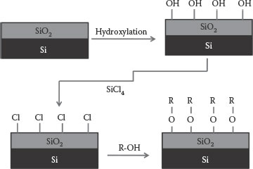
FIGURE 4.2 Formation of SAM on SiO2 involving the initial chlorination of the surface followed by reaction with R-OH.
Porphyrins are derived from the tetrapyrrole porphin molecule. They are aromatic conjugated molecules and can bind to all metals of the periodic table to form metalloporphyrins. In the real world, chlorophyll contains porphyrin with a magnesium central metal ion, and the Fe(II)porphyrin complex is a part of the hemoglobins and myoglobins, which transport oxygen in living beings [23]. Porphyin derivatives have numerous applications in pressure-sensitive paints, biosensors, gas sensors, and thin-film transistors [24, 25, 26 and 27]. Moreover, combining porphyrins with other organic semiconductors or devices interestingly led to novel concepts for sensing applications. For example, poly(3-hexylthiophene) (P3HT) and Cu(II)tetraphenyl porphyrin composite-based OFETs were demonstrated as sensors for the nitro-based explosive compounds [28]. Iron(III)porphyrin coated on an SU-8 micro cantilever probe with an integrated piezoresistive readout was shown as a carbon monoxide (CO) sensor [29]. Imahori and Fukuzumi [30] developed molecular photovoltaic devices by self-assembly of porphyrins and fullerenes on Au and indium tin oxide (ITO) electrodes. In these systems, porphyrins act as electron donors and fullerenes (C60) as electron acceptors. In their work, thiol chemistry was used for porphyrin monolayer formation on gold and porphyrin-C60 dyads were combined with SAMs on ITO.
4.3 ISSUES RELATED TO CMOS SCALING
Miniaturization of CMOS devices has major advantages like increased processing power, higher transistor density, and reduced cost per transistor. But, the scaling also leads to short-channel effects (SCEs) like increased leakage currents, hot-carrier injections, and increased source–drain resistance [31,32]. Besides SCEs, in the nano-CMOS regime, there are challenges in the back-end-of-line (BEOL) processes such as increased line resistance. Though low-k dielectrics enable interconnect scaling, they pose leakage and reliability problems [33,34]. Coming to front-end-of-line (FEOL), for the 45 nm node and beyond, high-k/metal-gate technologies have been explored to reduce leakage currents and reliable high-speed operation [35]. For this, high-k materials, including hafnium oxide (HfO2) and Al2O3, are investigated to replace the silicon dioxide gate dielectric. Concurrently, mid-gap metals and dual work function metals are suggested to eliminate effects such as poly-silicon depletion and poly-silicon dopant penetration. To achieve acceptable threshold voltage (Vt), gate electrodes must have appropriate work functions. In this scenario, metal gate work function tuning is an important process step to optimize device performance in nanoscale technologies.
New channel materials with improved transport properties (heterogeneous integration), such as SiGe, Ge, III–V semiconductors, and contemporary device structures, are being investigated to endorse CMOS scaling [36]. Graphene draws immense interest because of its electronic properties such as ballistic carrier transport and quantum Hall effect, thus making it a promising material and building block of future electronic devices and as a possible channel material for CMOS scaling. In spite of graphene’s amazing properties, there are some hurdles to surmount before it could be considered as a viable candidate to replace silicon. The most important challenges with graphene are the absence of band gap and ambipolar conduction that must be addressed to facilitate graphene’s use in logic devices and digital electronics [37].
In the following sections, we discuss the applications of metalloporphyrin SAMs as copper diffusion barriers, for work function tuning, and for tuning carrier injection in graphene FETs by forming zinc–porphyrin SAMs at the source–drain interface.
4.4 PORPHYRIN SAMS AS COPPER DIFFUSION BARRIERS
This section presents the application of zinc–porphyrin SAMs as Cu diffusion barriers for advanced back-end CMOS technologies. The SAM layers are integrated with various inter-layer dielectrics (ILDs) such as SiO2, hydrogen silsesquioxane (HSQ), and black diamond (BD).
4.4.1 COPPER/LOW-k TECHNOLOGIES IN ULSI METALLIZATION
Resistor–capacitor (RC) parasitics play a prominent role in overall chip performance in ultra-large scale integration (ULSI) technologies. That is why, in current technologies, copper metallization is used due to its lower resistivity (1.8 μΩ cm) as compared with traditional Al metallization (3.3 μΩ cm) [38,39]. In addition, the low-k dielectric between interconnects results in a significant reduction in RC delay, extending the performance enhancement curve for at least one technology generation [40]. Among various low-k materials, silsesquioxane (elementary unit (R–SiO3/2)n)-based dielectrics, with a k value less than that of SiO2’s relative permittivity, such as HSQ and methyl-silsesquioxane (CH3–SiO3/2 (MSQ)), have been widely explored [41,42]. Amorphous carbon and polymers have also been explored for BEOL purposes [43,44]. Lowering the k values in silica-based materials can be achieved by doping with fluorine or carbon or by introducing CH3 groups [45]. Also, BD is a low-k film from Applied Materials, consisting of PECVD organosilicate material with a changeable organic phase [46]. Though Cu/low-k technologies provide solutions to CMOS scaling, there are reliability issues such as copper diffusion through ILD, copper drift, poor adhesion, and thermal stability [47,48].
Thus, Cu needs an appropriate diffusion barrier which is scalable along with other device dimensions [49,50].
4.4.2 CU DIFFUSION BARRIERS IN ULSI METALLEZATION
Present CMOS technology node is 22 nm and following the 32 nm node. Future CMOS technology nodes are 15 nm, 14 nm etc., need ultrathin Cu diffusion barriers [51]. Sputtered TaN or ternary nitride alloys, such as W–Ge–N, Ta–Si–N, and Ta–W–N, deposited using reactive sputtering, can act as diffusion barriers [52, 53, 54 and 55], but we realize that thinner barriers are problematic with this kind of deposition. Barrier layers deposited by atomic layer deposition (ALD) are thinner as compared to sputtered films, but they tend to have high-defect densities and grain boundaries [56]. On the other hand, self-forming diffusion barriers reduce the overall Cu conductivity [57, 58 and 59]. Alternately, SAMs with step coverage can be used as diffusion barriers. They are formed either by vapor-phase self-assembly or by wet chemical methods. Organosilane monolayers can inhibit Cu diffusion into SiO2 and it was observed that the size and configuration of the terminal functional group and molecular chain length play an important role in the barrier properties. SAMs with long-chain lengths screen Cu atoms from the influence of the substrate and the aromatic rings sterically hinder Cu diffusion between the molecules through the SAM layer [6061, 62 and 63].
The following subsection presents the application of 5-(4-hydroxyphenyl)-10, 15, 20-tri (p-tolyl) zinc(II) porphyrin (Zn(II)TTPOH) SAMs as Cu diffusion barriers for advanced back-end CMOS technologies.
4.4.3 PORPHYRIN SAMS AS CU DIFFUSION BARRIERS IN ULSI METALLIZATION
4.4.3.1 Bias–Temperature–Stress Analysis
Cu diffuses through ILDs under high bias–temperature conditions [64]. The diffused charge leads to a lateral shift of voltage in the capacitance–voltage (CV) curves. Bias-temperature stress (BTS) studies were carried out on Cu/SiO2/p-Si and Cu/SAM/SiO2/p-Si MOSCAP (metal–oxide–silicon capacitors) test structures to characterize the Cu diffusion (device fabrication procedure, SAM formation can be found in ref. 65). Figure 4.3 shows the schematic representation of MOSCAP used in this study and the Zn(II)TTPOH molecule used for SAM preparation.
Figure 4.4a describes the pre-stress and post-stress C−V characteristics for the MOS capacitors (EOT = 40 nm) with and without the porphyrin SAM, obtained at 50 kHz frequency, using the Agilent 4284-A precision LCR meter. In this study, a Cu/SiO2/p-Si MOS capacitor was subjected to 2.5 MV/cm electric field stress at 100°C for 30 min, whereas the Cu/SAM/SiO2/p-Si MOS capacitor was subjected to 4.5 MV/cm electric field stress at 100°C for 30 min. Comparing the C−V plots, it is evident that the C−V curve shift is less in the case of the Cu/SAM/SiO2/Si MOS structure compared to that of the MOS structure without SAM [65]. This shows the effectiveness of Zn porphyrin SAM as a Cu diffusion barrier. Figure 4.4b shows the HFCV (hydrogen fuel-cell vehicle) characteristics of the Cu/HSQ/p-Si and Cu/SAM/HSQ/p-Si MIS test structures [66]. Comparing the CV plots in Figure 4.4b, it is clear that the C−V curve shift is less in the case of the Cu/SAM/HSQ/Si MIS structure compared to that of the MIS structure without SAM.
BTS studies (to evaluate barrier performance) were also performed on the MIS capacitor structures with BD as the dielectric. The devices were subjected to a stress of 1.25 MV/cm at 100°C. The CV curves obtained for devices without SAM and with SAM are shown in Figure 4.5. After stress, devices without SAM degraded to a higher extent as compared to devices with SAM [67].
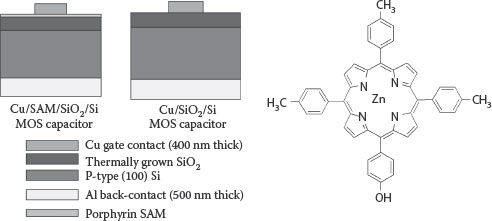
FIGURE 4.3 Device schematic and 5-(4-hydroxyphenyl)-10, 15, 20-tri (p-tolyl) zinc(II) porphyrin molecule.
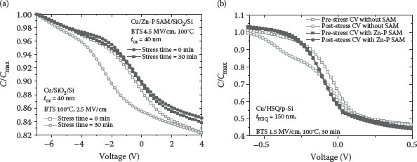
FIGURE 4.4 (a) Pre-stress and post-stress C−V characteristics for the Cu MOS capacitors with and without the porphyrin SAM. (M. A. Khaderbad et al., Metallated porphyrin self assembled monolayers as Cu diffusion barriers for the nano-scale CMOS technologies, 8th IEEE Conference on Nanotechnology, 2008. NANO ’08. Arlington, Texas, pp. 167–170. © (2008) IEEE. With permission.) (b) Pre-stress and post-stress C−V characteristics for the MIS capacitors with and without the porphyrin SAM. U. Roy et al., Hydroxy-phenyl Zn(II) porphyrin self-assembled monolayer as a diffusion barrier for copperlow k interconnect technology, Electron Devices and Semiconductor Technology, 2009. IEDST ’09. 2nd International Workshop on, pp. 1–5. © (2009) IEEE. With permission.)
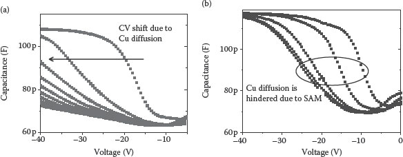
FIGURE 4.5 BTS C−V characteristics (a) for the Cu/BD/Si MIS capacitors. (b) BTS CV with porphyrin SAM. (M. A. Khaderbad et al., Porphyrin Self-assembled monolayer as a copper diffusion barrier for advanced CMOS technologies, Electron. Dev., IEEE Trans., 99, 1–7. © (2012) IEEE. With permission.)
4.4.3.2 Secondary Ion Mass Spectrometry
To observe the diffusion of Cu in ILD, the time-of-flight secondary ion mass spectrometry (ToFSIMS) was acquired using a TRIFT V nano-TOF instrument manufactured by Physical Electronics, MN, USA. Figure 4.6a shows the SIMS depth profile of Cu in the Cu/SiO2/Si and Cu/SAM/SiO2/Si samples, annealed at 400°C in N2 atmosphere for 1 h. The ILD thickness is around 150 nm. It can be clearly observed that the Cu has penetrated more into the sample in which there is no SAM barrier [67]. This shows the effectiveness of the Zn(II)TTPOH monolayer as a good barrier layer to copper diffusion into SiO2. Similar results are observed in samples with BD ILD (Figure 4.6b) samples, annealed at 300°C, for 30 min in N2 atmosphere.
The observed BTS and SIMS analysis trends indicate that zinc porphyrin monolayers act as efficient copper diffusion barriers for porous low-k ILDs. Besides, no change in bulk permittivity or the bulk mechanical properties of the ILD were observed after SAM integration. This work clearly shows that the bottom-up grown monolayers on ILDs improve the device reliability by hindering Cu diffusion without affecting the ILD film bulk properties [6566 and 67].
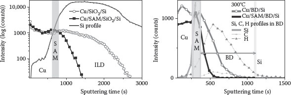
FIGURE 4.6 SIMS depth profile of copper is obtained with the Cu/SiO2/Si and Cu/SAM/SiO2/Si structures after annealing for 1 h in N2 atmosphere. Si profile (Cu-ILD interface) can also be seen in the figure SIMS depth profile of copper obtained with the Cu/BD/Si and Cu/SAM/BD/Si structures after annealing for 1 h in N2 atmosphere. (M. A. Khaderbad et al., Porphyrin Self-assembled monolayer as a copper diffusion barrier for advanced CMOS technologies, Electron. Dev., IEEE Trans., 99, 1–7. © (2012) IEEE. With permission.)
The following section presents a technique for the tuning of the gate metal work function (Φmetal) using SAMs of metalloporphyrins.
4.5 PORPHYRIN SAMS FOR METAL GATE WORK FUNCTION TUNING
Among various components, the MOSFET gate is an important entity in the overall transistor design and scaling. New technical challenges and SCEs arise with the scaling of feature sizes in the sub-nanometer technological regime [68,69]. The demand for gate engineering has been driven by various technical concerns [70]. For example, p-type metal-oxide-semiconductor (PMOS) and n-type metal-oxide-semiconductor (NMOS) need low and symmetrical threshold voltages (Vt) for proper switching, high-performance, and for low-power applications. In the case of polysilicon gates, this was achieved by different threshold-adjustment implants for n-type and p-type devices [71]. But, boron penetration, which is a side effect of gate doping, causes charge trapping at the gate–oxide interface, impurity diffusion into gate oxide, and uncontrollable transistor threshold voltages. Moreover, high doping levels in the polysilicon gate result in polydepletion effects for ultra-thin oxide MOSFETs due to the serial connection of the smaller polydepletion capacitance with oxide capacitance. This leads to the degradation of inversion gate capacitance and transconductance, and drive currents [72,73]. One alternate method to solve the above problems is to use metal gates instead of polysilicon [74,75]. Also, the thickness of the silicon dioxide (SiO2) dielectric or its Si–O–N analogue is becoming sufficiently thin that the direct gate tunnelling currents through the dielectrics are posing reliability problems, increased power dissipation, and eventually deteriorate the device performance and circuit stability for VLSI circuits [76,77]. A solution to the problem is the replacement of SiO2 by an alternative insulator with a higher dielectric constant, so that the physical thickness of the dielectric could be increased [7879 and 80].
4.5.1 POTENTIAL GATE ELECTRODES FOR WORK FUNCTION ENGINEERING
The Vt of a MOSFET mainly depends on the gate work function. For bulk devices, the required metal work functions for replacing the conventional n- and p-polysilicon gates are about 4 and 5 eV, respectively, to control Vt swings. In other words, for NMOS and PMOS devices to have low and symmetric threshold voltages, two gate electrodes with different work functions are needed. This calls for the integration of multiple metals on a single substrate. In such processes, transition metals such as W, Ti, Ta, Mo, and Ru, and their metallic derivatives, WN, TiN, TaN, MoN, TaSiN, and MoSiN are used as metal gates. These transition metals are known to possess some desirable properties such as mid-gap work function, high melting point, low resistivity, and high thermal stability [8182 and 83].
However, the use of two different metals for PMOS and NMOS devices may require a complicated, selective deposition and etching process for integration onto the same silicon substrate. However, in another approach, a single metal with a tunable work function can be used. Using a single metal is simpler from a process integration perspective. This tuning has been successfully implemented using various techniques, including alloying, metal inter-diffusion, dopant implantation, silicidation, and nitridation [8485 and 86]. Also, SAMs of dipolar organic molecules at the metal electrode and gate dielectric interface can be used to selectively tune the work function. Molecules in SAM create an effective dipole at the interface, which enables the change in metal work function [87,88]. By means of first principles study, Heimel et al. [89] had shown that the local ionization potential and electron affinity, together with the interface dipole, determine the work function modification.
4.5.2 PORPHYRIN SAMS FOR WORK FUNCTION ENGINEERING
Here, TTPOH molecules with different central metal ions have been used to form SAMs on SiO2, HfO2, and Al2O3 gate dielectrics. Moreover, dipolar properties of porphyrin macrocycles can be tuned by incorporating various metal species in them or by using various subgroups. This allows work-function tuning for different technological applications. The Kelvin probe force microscopy (KPFM) characterizations of SAMs show local changes in the surface potential induced by the alignment of molecular dipole moments. Figure 4.7a depicts KPFM imaging of patterned Zn(II) TTPOH SAM on Si, showing higher potential with respect to Si substrate. Figure 4.7b shows the surface potential of Mg, Fe, Co, and Zn TTPOH SAMs on Si. Figure 4.7c shows the estimated dipole moments of metallo-TTPOH molecules using DFT (density functional theory) calculations (performed using the DMol3 module in the Accelrys Materials Studio [91]). It can be clearly seen that TTPOH with Co has less dipole moment as compared to that with Zn central metal.
The chemical structure of TTPOH with different central metal ions for SAM preparation is shown in Figure 4.8a.
For work-function tuning experiments, Al/SiO2/Si and Al/SAM/SiO2/Si MOSCAP test structures were fabricated (fabrication procedure can be found in ref. [92]). HFCV technique was used to measure the flat-band voltage (Vfb), the work function difference (Φms), and other important electrical parameters. The C–V curves for bare SiO2 (3–4 nm thick) and the SiO2 surface covered with TTPOH SAM with various metal derivatives are presented in Figure 4.8. The dipolar SAM layer at the metal–oxide interface modifies the potential, thereby changing the effective metal work function. This can be given as below
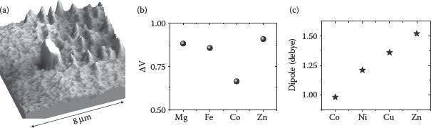
FIGURE 4.7 (a) KPFM image showing 30 mV potential corresponding to the SAM dipole [90]. (b) Surface potential measured for TTPOH SAMs with different transition metal atoms. (c) Dipole moment estimated from DFT calculations.
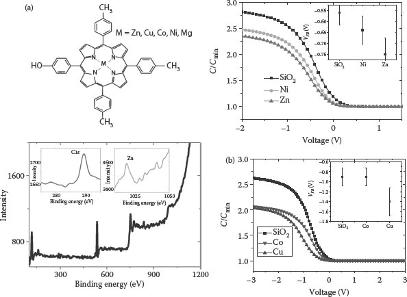
FIGURE 4.8 (a) 5-(4-Hydroxyphenyl)-10,15,20-tri(p-tolyl) porphyrin with different central metal ions and an XPS spectrum of Zn(II)TTPOH SAM on SiO2. (b) HFCV plots Al/SiO2/p-Si, Al/(Zn/Ni) porphyrin SAM/SiO2/p-Si MOS CAPs (tox = 3 nm), and Al/SiO2/p-Si, Al/(Cu, Co) porphyrin SAM/SiO2/p-Si MOS CAPs (tox = 3.5 nm). (M. A. Khaderbad et al., Variable interface dipoles of metallated porphyrin self-assembled monolayers for metal-gate work function tuning in advanced CMOS technologies, IEEE Trans. Nanotechnol., 9(3), 335–337. © (2010) IEEE. With permission.)
(4.1) |
where Φms,mod is the modified metal work function due to SAM.
For work-function tuning experiments on high-k dielectrics, HfO2 was deposited on a p-type (100) Si wafer using an AMAT gate stack cluster tool with an integrated CVD chamber for MOCVD of high-k materials. Tetrakis(diethylamino)hafnium (TDEAH) was used as a precursor in thin-film deposition with oxygen as the oxidant gas [79,93].
Figure 4.9a illustrates the ground state UV–Vis reflection spectra of the Zn(II)TTPOH SAM on HfO2, clearly showing the presence of Zn(II)TTPOH. Figure 4.9b shows the C–V curves of bare HfO2 (EOT~5.46 nm) and the HfO2 surface covered with Zn-TTPOH SAM (EOT~5.59 nm) [94]. Figure 4.9b also shows the hysteresis analysis on the above MOSCAPs.
Further, similar experiments were performed on devices with high-k Al2O3 [94]. Al2O3 deposition was done by reactive sputtering using a pulsed DC power supply [95,96]. Figure 4.10a shows the XPS spectrum of Zn(II)TTPOH SAM on Al2O3 and in the UV–Vis spectra of SAM on Al2O3, and the peak around 429 nm clearly shows the presence of Zn(II)TTPOH porphyrin (Figure 4.10b).
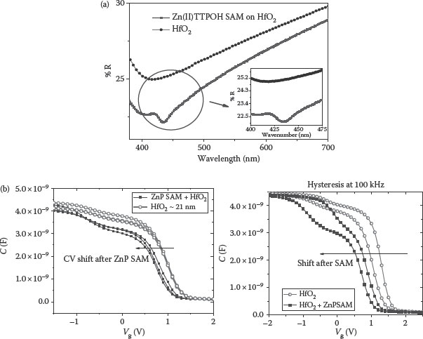
FIGURE 4.9 (a) UV reflection spectra SAM on HfO2. (b) HFCV plots (tHfO2~21 nm) showing a shift due to ZnP SAM formation on HfO2 and hysteresis analysis on MOSCAPs (tHfO2~21 nm) showing a shift due to ZnP SAM formation on HfO2. (M. A. Khaderbad et al., Bottom-up method for work function tuning in high-k/metal gate stacks in advanced CMOS technologies, 11th IEEE Conference on, Nanotechnology, 2011. NANO ’11. Portland, Oregon, pp. 269–273. © (2011) IEEE. With permission.)
Figure 4.11 shows the HFCV curves of bare Al2O3 (~15 nm thick and k~7) and Al2O3 with Cu and Ni TTPOH SAMs. As seen in the figure, the metal-gate work function was modified successfully by the adsorbed molecules and Cu(II)TTPOH SAM shows a higher shift as compared to Ni(II)TTPOH SAM. Figure 4.11b shows HFCV curves for the 5.22 nm Al2O3 MOSCAP with and without Cu(II) TTPOH SAM, with EOTs of 3.32 and 2.91 nm, respectively (shift~−0.79 V).
Figure 4.12a presents the flat-band voltage values for Al2O3 thicknesses. A constant shift in the presence of Cu(II)TTPOH SAM shows that the change in the magnitude of work function (|ΔΦms| ~ 0.8 V) arises from the dipole moment associated with the organic monolayer. To see the effect of temperature, the devices were exposed to annealing conditions of 400°C for an hour in ambient N2. CV characteristics were obtained for these devices before and after annealing and are shown in Figure 4.12b. HFCV curves show that the devices are intact after exposure to these processing conditions of temperature. This shows that the above technique can be very effective in advanced CMOS technologies involving gate-last CMOS processes.
Thus, in porphyrins, central metal ion, substituents, their position, monolayer assembly, and intramolecular interactions have an effect on the value of dipole and subsequent electronic properties.
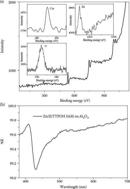
FIGURE 4.10 (a) XPS spectrum of the UV reflection spectra SAM on HfO2. (b) UV reflection spectra of SAM on Al2O3. (M. A. Khaderbad et al., Bottom-up method for work function tuning in high-k/metal gate stacks in advanced CMOS technologies, 11th IEEE Conference on, Nanotechnology, 2011. NANO ’11. Portland, Oregon, pp. 269–273. © (2011) IEEE. With permission.)
4.6 UNIPOLAR GRAPHENE FIELD EFFECT TRANSISTORS BY MODIFYING SOURCE AND DRAIN ELECTRODE INTERFACES WITH ZN(II)TTPOH
This section refers to the unipolar operation of reduced graphene oxide (RGO) FETs by modification of source–drain (S–D) electrode interfaces with SAMs of Zn(II)TTPOH molecules.
Graphene, a two-dimensional network of carbon atoms, has sparked interest in the research community because of its unique electrical and mechanical properties. It has a large specific surface area, high intrinsic mobility, high Young’s modulus, and thermal conductivity [95]. Reduced graphene oxide (RGO), which is a solution processed form of graphene, is being considered in electrical, energy, and sensor applications [96]. The lower carrier mobilities in RGO FETs (in comparison to pristine graphene) [97] are due to the presence of defects and a disconnected network of π-delocalized regions in the carbon atom arrangement. The ambipolar conductance in RGO makes it unsuitable for fabricating logic gates or circuits. This is because the power consumption is higher in such circuits compared to unipolar logic. Previous attempts to achieve unipolar transport in graphene include nitrogen doping or the utilization of cobalt electrodes in graphene FETs, resulting in asymmetric electron hole currents in the devices [98,99].
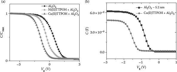
FIGURE 4.11 HFCV curves for Al2O3 as a gate dielectric with (a) thickness = 15 nm and (b) thickness = 5.22 nm. (M. A. Khaderbad et al., Bottom-up method for work function tuning in high-k/metal gate stacks in advanced CMOS technologies, 11th IEEE Conference on Nanotechnology, 2011. NANO ’11. Portland, Oregon, pp. 269–273. © (2011) IEEE. With permission.)
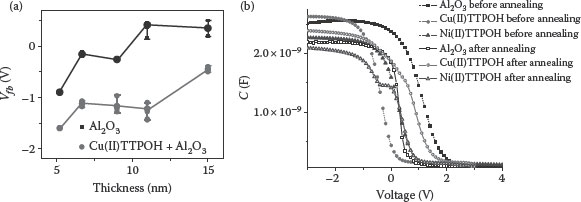
FIGURE 4.12 (a) Plot of flatband voltage versus the thickness with the corresponding error bars and (b) CV curves obtained before and after annealing at 400°C.
4.6.2 ELECTRICAL TRANSPORT MODIFICATION IN RGO FETS USING PORPHYRIN SAMS
Interface or surface modification through molecular self-assembly provides a way to modify the electronic properties of devices at lower costs [100]. In general, the hole and electron injection barrier heights are determined by the differences between the metal electrode work function (φ) and the highest occupied molecular orbital (HOMO) or the lowest unoccupied molecular orbital (LUMO) of the semiconductor. However, through the integration of dipoles at metal–semiconductor interfaces, the barrier heights can be modulated, significantly affecting the charge injection [101]. Chen et al. have used self-assembled functionalized aromatic thiols to tune the hole injection barrier (φh) of copper(II) phthalocyanine on Au(111) [102].
Here, controlling carrier injection in graphene FETs with the integration of Zn(II)TTPOH SAM at the electrode interfaces of RGO transistors has been reported. SAM and device fabrication havebeen reported elsewhere [103]. Figure 4.13 shows the SEM images of the fabricated devices.
Figure 4.14a shows the interface energy level diagram of RGO with Pt electrodes before and after SAM modification. As shown in this figure, barrier heights required for charge injection from a metal to the semiconductor with Zn(II)TTPOH interfacial modification can be expressed as [104]
(4.2) |
(4.3) |
where φM is the work function of the electrode, χ is the electron affinity (LUMO), and Eg is the band gap of the Zn-porphyrin; Δ φdipole is the barrier change due to the interface dipole.
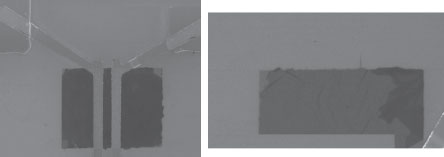
FIGURE 4.13 SEM images of the fabricated devices. (Reprinted with permission from M. A. Khaderbad et al., Fabrication of unipolar graphene field effect transistors by modifying source and drain electrode interfaces with Zn-porphyrin, ACS Appl. Mater. Interfaces, 4(3), 1434–1439. Copyright 2012, American Chemical Society.)
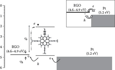
FIGURE 4.14 Schematic representation of the SAM-modified source (drain) interface (inset shows the RGO-Pt interface). (Reprinted with permission from M. A. Khaderbad et al., Fabrication of unipolar graphene field effect transistors by modifying source and drain electrode interfaces with Zn-porphyrin, ACS Appl. Mater. Interfaces, 4(3), 1434–1439. Copyright 2012, American Chemical Society.)
In this work, energy levels of Zn(II)TTPOH were measured using cyclic voltammetry. In a cyclic voltammogram, the onset of oxidation is related to the HOMO energy level and the LUMO energy level can be estimated from the reduction potential. For Zn(II)TTPOH, first oxidation occurs at 0.68 V and first reduction occurs at −1.41 V. These values correspond to the HOMO level of 5.1 eV and LUMO level of 2.97 eV, respectively. Zn(II)TTPOH dipole (Δ φdipole) was estimated from the surface potential measurements of Zn(II)TTPOH SAM on RGO using KPFM. From the KPFM values and the HOMO–LUMO levels of Zn(II)TTPOH calculated from CV, φe and φh can be calculated (from Equations 4.2 and 4.3) as 2.2 and 0.11 eV, respectively, showing a higher barrier for electrons as compared to holes. At the metal–organic interfaces, the injection current I is described as follows [105]:
(4.4) |
where A is the injecting area, Ψ is a slowly varying function of the electric field, N0 is the density of the unoccupied sites in the semiconductor, μ is the bulk mobility of the injected charge carriers in the organic semiconductor, E is the electric field, φB is the height of the injection barrier, kB is the Boltzmann’s constant, and T is the temperature.
As injection current I α exp(− φB/kBT), a higher injection barrier for electrons as compared to that of holes is the source of unipolar behavior in Zn porphyrin-modified graphene FETs. This is clearly observed in the IV characteristics of Zn porphyrin-modified graphene FETs (Figure 4.15). The fabrication of these devices is explained elsewhere [103].
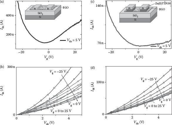
FIGURE 4.15 (a) Transfer characteristics of the RGO FET for Vds = 5 V (a schematic of the device is shown in the inset). (b) Output characteristics of RGO FETs. (c) Transfer characteristics of the RGO-SAM FET for Vds = 5 V. (d) Output characteristics of RGO-SAM FETs for different gate voltages. (Reprinted with permission from M. A. Khaderbad et al., Fabrication of unipolar graphene field effect transistors by modifying source and drain electrode interfaces with Zn-porphyrin, ACS Applied Materials & Interfaces, 4(3), 1434–1439. Copyright 2012, American Chemical Society.)
Figure 4.15b shows the output characteristics of the graphene device showing the electron modulation and the hole transport by the applied gate voltage.
This chapter explains the bottom-up approaches for CMOS scaling in the nanoscale era. In the BEOL processes, it has been shown that porphyrin SAMs can be used as effective copper diffusion barriers, thus improving the device performance and lifetime. BTS and SIMS studies confirm the effectiveness of zinc-porphyrin SAM as a good copper diffusion barrier. No change in permittivity of the ILD was observed with SAM integration. Nanoindentation measurements on BD films show that there is no effect on the bulk mechanical properties of BD because of SAM integration.
In the front-end-of-line (FEOL), a technique to modify the magnitude of metal work function is demonstrated by changing the central metal ion (Zn, Co, Cu, Ni) in the porphyrin SAM on SiO2, HfO2, and Al2O3 gate dielectrics. KPFM and DFT simulations of porphyrin SAMs and porphyrins show that the variation in dipole moment in porphyrins can be achieved by changing the central metal ion. HFCV analysis on MOSCAPs with different EOTs shows that the shift in flat-band voltage is due to the dipole moment associated with central metal ion in the porphyrin ring. Hence, this technique has a potential for applications in CMOS technologies involving the gate last processes.
Also, bottom-up fabrication methods can be used for interface engineering of nanoelectronic devices. Zn(II)TTPOH treatment of RGO at the source–drain interface inhibits electron injection by increasing the barrier height for electrons at the RGO–Pt interface. This work clearly demonstrates that relevant interface modifications using SAM provide a powerful approach to improve the performance of RGO FETs and are critical for applications such as logic gates and integrated circuitry.
1. E. J. Nowak, Maintaining the benefits of CMOS scaling when scaling bogs down, IBM J. Res. Dev., 46(2–3), 169–180, 2002.
2. Y. Ando, K. Miyake, A. Mizuno, A. Korenaga, M. Nakano, and H. Mano, Fabrication of nanostripe surface structure by multilayer film deposition combined with micropatterning, Nanotechnology, 21, 095304, 2010.
3. S. Samukawa, Ultimate top-down etching processes for future nanoscale devices: Advanced neutralbeam etching, Jpn. J. Appl. Phys., 45(4A), 2395–2407, 2006.
4. J. Lian, L. Wang, X. Sun, Q. Yu, and R. C. Ewing, Patterning metallic nanostructures by ion-beam-induced dewetting and Rayleigh instability, Nano Letters, 6(5), 1047–1052, 2006.
5. W. Lu and C. M. Lieber, Nanoelectronics from the bottom-up, Nat. Mater., 6, 841–850, 2007.
6. N. Nuraje, S. Mohammed, L. Yang, and H. Matsui, Biomineralization nanolithography: Combination of bottom-up and top-down fabrication to grow arrays of monodisperse gold nanoparticles along peptide lines, Angew. Chem. Int. Ed., 48, 2546–2548, 2009.
7. T. Kamins, Beyond CMOS electronics: Self-assembled nanostructures, Springer Ser. Mater. Sci., 106, Part III, 227–256, 2009.
8. B. Yu and M. Meyyappan Nanotechnology: Role in emerging nanoelectronics, Solid-State Electron., 50, 536–544, 2006.
9. Y. Huang, X. F. Duan, Y. Cui, L. J. Lauhon, K.-Ha Kim, and C. M. Lieber, Logic gates and computation from assembled nanowire building blocks, Science, 294(5545), 1313–1317, 2001.
10. M. A. Khaderbad, A. Kushagra, M. Ravikanth, and V. Ramgopal Rao, Bottom-up approaches for nanoelectronics, Cutting Edge Nanotechnology, D. Vasileska (Ed.), 2010, ISBN: 978-953-7619-93-0, INTECH, Croatia.
11. K. Nayak, P. Kulkarni, A. Deepu, V. Sitaraman, S. Punidha, A. Saha, M. Ravikanth, S. Mitra, S. Mukherji, and V. R. Rao, Patterned microfluidic channels using self-assembled hydroxy-phenyl porphyrin monolayer, Proceedings of the 7th IEEE International Conference on Nanotechnology, August 2–5, Hong Kong, 2007.
12. G. M. Whitesides and B. Grzybowski, Self-assembly at all scales, Science, 295, 5564, 2418, 2002.
13. Y. Xia, X. Zhao, and G. M. Whitesides, Pattern transfer: Self-assembled monolayers as ultrathin resists, Microelectron. Eng., 32(1–4), Nanotechnology, 255–268, 1996.
14. U. Srinivasan, M. R. Houston, R. T. Howe, and R. Maboudian, Alkyltrichlorosilane based self-assembled monolayer films for stiction reduction in silicon micromachines, J. Microelectromech. Syst, 7, 252–60, 1998.
15. F. Schreiber, Structure and growth of self-assembling monolayers, Progr. Surf. Sci., 65, 151–256, 2000.
16. J. Sagiv, Organized monolayers by adsorption. 1. Formation and structure of oleophobic mixed monolayers on solid surfaces, J. Am. Chem. Soc., 102(1), 92–98, 1980.
17. A. Ulman, Formation and structure of self-assembled monolayers, Chem. Rev. 96, 1533–1554, 1996.
18. D. K. Aswal, S. Lenfant, D. Guerin, J. V. Yakhmi, and D. Vuillaume, Self assembled monolayers on silicon for molecular electronics, Anal. Chim. Acta, 568, 84–108, 2006.
19. R. C. Major and X.-Y. Zhu, Two-step approach to the formation of organic monolayers on the silicon oxide surface, Langmuir, 17(18), 5576–5580, 2001.
20. W. Gao, L. Dickinson, C. Grozinger, F. G. Morin, and L. Reven, Self-assembled monolayers of alkylphosphonic acids on metal oxides, Langmuir, 12(26), 6429–6435, 1996.
21. A. Raman, M. Dubey, I. Gouzman, and E. S. Gawalt, Formation of self-assembled monolayers of alkylphosphonic acid on the native oxide surface of SS316 L, Langmuir, 22(15), 6469–6472, 2006.
22. D. L. Angst and G. W. Simmons, Moisture absorption characteristics of organosiloxane self-assembled monolayers, Langmuir, 7(10), 2236–2242, 1991.
23. D. Dolphin, The porphyrins, Physical Chemistry, Part C, Academic Press, New York, 1978.
24. S. Grenoble, M. Gouterman, G. Khalil, J. Callis, and L. Dalton, Pressure-sensitive paint (PSP): Concentration quenching of platinum and magnesium porphyrin dyes in polymeric films, Elsevier J. Lumin. 113, 33–44, 2005.
25. D. B. Papkovsky, T. O’Riordan, and A. Soini, Phosphorescent porphyrin probes in biosensors and sensitive bioassays, Biochem. Soc. Trans., 28, 74–77, 2000.
26. S. Tao and G. Li, Porphyrin-doped mesoporous silica films for rapid TNT detection, Colloid Polym Sci., 285, 721–728, 2007.
27. P. Checcoli, G. Conte, S. Salvatori, R. Paolesse, A. Bolognesi, M. Berliocchi, F. Brunetti, A. D’Amico, A. Di Carlo, and P. Lugli, Tetra-phenyl porphyrin based thin film transistors, Synth. Metals, 138(1–2), 261–266, 2003.
28. R. S. Dudhe, S. P. Tiwari, H. N. Raval, M. A. Khaderbad, J. Sinha, M. Yedukondalu, M. Ravikanth, A. Kumar, and V. R. Rao, Explosive vapour sensor using poly (3-hexylthiophene) and Cu-tetraphenyl-porphyrin composite based organic field effect transistors, Appl. Phys. Lett., 93, 263306, 2008.
29. C. Vijaya Bhaskar Reddy, M. A. Khaderbad, S. Gandhi, M. Kandpal, S. Patil, K. Narasaiah Chetty, K. Govinda Rajulu, P. C. K. Chary, M. Ravikanth and V. Ramgopal Rao, Piezoresistive SU-8 cantilever with Fe(III)porphyrin coating for CO sensing, Nanotechnology, IEEE Transactions on, PP(99), 1, 2012.
30. H. Imahori and S. Fukuzumi, Porphyrin- and fullerene-based molecular photovoltaic devices, Adv. Funct. Mater., 14(6), 525–536, 2004.
31. D. J. Frank, R. H. Dennard, E. K. Nowak, P. M. Solomon, Y. Taur, and H-S. P. Philip Wong, Device scaling limits of Si MOSFETs and their application dependencies, Proceedings of the IEEE, 89(3), 259–287, 2001.
32. B. P. Wong, A. Mittal, Y. Cao, and G. Starr, Nano-CMOS Circuit and Physical Design, Chapter 1, Wiley, New Jersey, 2004, ISBN: 978-0-471-46610-9.
33. K. Maex, M. R. Baklanov, D. Shamiryan, F. lacopi, S. H. Brongersma, and Z. S. Yanovitskaya, Low dielectric constant materials for microelectronics, J. Appl. Phys., 93(11), 8793–8841, 2003.
34. C. D. Hartfield, E. T. Ogawa, Y-J. Park, T-C. Chiu, and H. Guo, Interface reliability assessments for copper/low-k products, Device Mater. Reliab., IEEE Trans., 4(2), 129–141, 2004.
35. R. Chau, S. Datta, M. Doczy, B. Doyle, J. Kavalieros, and M. Metz, High-K/metal-gate stack and its MOSFET characteristics, IEEE Electron Dev. Lett., 25(6), 408–410, June 2004.
36. T. Skotnicki, J. A. Hutchby, T-J. King, H-S, P. Wong, and F. Boeuf, Toward the introduction of new materials and structural changes to improve MOSFET performance, 2005, Circuits Dev. Mag., IEEE, 21(1), 16–26.
37. S. K. Banerjee, L. F. Register, E. Tutuc, D. Basu, S. Kim, D. Reddy, and A. H. MacDonald, Graphene for CMOS and beyond CMOS applications, Proc. IEEE, 98(12), 2032–2046, 2010.
38. H. Havemann and J. A. Hutchby, High-performance interconnects: An integration overview, Proc. IEEE, 89(5), 586–601, 2001.
39. S. P. Murarka, Multilevel interconnections for ULSI and GSI era, Mater. Sci. Eng. R: Reports, 19(3–4), 87–151, 1997.
40. B. Li, T. D. Sullivan, T. C. Lee, and D. Badami, Reliability challenges for copper interconnects, 2004, Microelectron. Reliab., 44(3), 365–380.
41. E. S. Moyer, K. Chung, M. Spaulding, T. Deis, R. Boisvert, C. Saha, and J. Bremmer, Ultra low dielectric constant silsesquioxane based resin [ILDs], Interconnect Technology, IEEE International Conference, San Francisco, CA, pp. 196–197, 1999.
42. H-J. Lee, E. K. Lin, H. Wang, W. Wu, W. Chen, and E. S. Moyer, Structural comparison of hydrogen silsesquioxane based porous low-k thin films prepared with varying process conditions, Chem. Mater., 14(4), 1845–1852, 2004.
43. D. T. Price, R. J. Gutmann, and S. P. Murarka, Damascene copper interconnects with polymer ILDs, Thin Solid Films, 308–309, 31, 523–528, 1997.
44. Jeremy A. Theil, Fluorinated amorphous carbon films for low permittivity interlevel dielectrics, J. Vac. Sci. Technol. B, 17, 2397, 1999.
45. K. J. Chao, P. H. Liu, A. T. Cho, K. Y. Huang, Y. R. Lee, and S. L. Chang, Preparation and characterization of low-k mesoporous silica films, Stud. Surf. Sci. Catal., Elsevier, 154, Part 1, 94–101, 2004.
46. W. H. Teh, C. F. Tsang, A. Trigg, K. W. Teoh, R. Kumar, N. Balasubramanian, D. L. Kwong, S. E. Ong, Farah Malik, and C. L. Gan, Adhesion studies of Ta/Low-k (black diamond) interface using thermocompressive wafer bonding and four-point bend, J. Electrochem. Soc., 153(9), G795–G798, 2006.
47. Y. Shacham-Diamond, D. A. Hoffstetter, and W. G. Oldham, Reliability of copper metallization on silicon-dioxide, VLSI Multilevel Interconnection Conference, IEEE, Santa Clara, CA, pp. 109–115, 1991.
48. G. B. Alers, K. Jow, R. Shaviv, G. Kooi, and G. W. Ray, Interlevel dielectric failures in copper/low-k structures, Dev. Mater. Reliab., IEEE Trans., 4(2), 148–152, June 2004.
49. Zs. Tokei, Y-L. Li, and G. P. Beyer, Reliability challenges for copper low-k dielectrics and copper diffusion barriers, Microelectron. Reliab., 45(9–11), 1436–1442, September 2005.
50. A. E. Kaloyeros and E. Eisenbraun, Ultrathin diffusion barriers/liners for gigascale copper metallization, Ann. Rev. Mater. Sci., 30, 363–385, 2000.
51. A. E. Kaloyerosa, E. T. Eisenbrauna, K. Dunna, and O. van der Straten, Zero thickness diffusion barriers and metallization liners for nanoscale device applications, Chem. Eng. Commun., 198(11), 1453–1481, 2011.
52. S. R. Burgess, H. Donohue, K. Buchanan, N. Rimmer, and P. Rich, Evaluation of Ta and TaN-based Cu diffusion barriers deposited by Advanced Hi-Fill (AHF) sputtering onto blanket wafers and high aspect ratio structures, Microelectron. Eng., 64(1–4), 307–313, October 2002.
53. J. Li, H-S. Lu, Y-W. Wang, X-P. Qu, Sputtered Ru-Ti, Ru-N, and Ru-Ti-N films as Cu diffusion barrier, Microelectron. Eng., 88(5), 635–640, May 2011.
54. S. Rawal, D. P. Norton, T. J. Anderson, and L. McElwee-White, Properties of W–Ge–N as a diffusion barrier material for Cu, Appl. Phys. Lett., 87, 111902, 2005.
55. M-A. Nicolet, Ternary amorphous metallic thin films as diffusion barriers for Cu metallization, Appl. Surf. Sci., 91(1–4), 269–276, October 1995.
56. C. H. Peng, C. H. Hsieh, C. L. Huang, J. C. Lin, M. H. Tsai, M. W. Lin, C. L. Chang, W. S. Shue, and M. S. Liang, A 90 nm generation copper dual damascene technology with ALD TaN barrier, IEDM, 603–606, 2002.
57. J. Koike and M. Wada Self-forming diffusion barrier layer in Cu-Mn alloy metallization, Appl. Phys. Lett., 87, 041911, 2005.
58. D-C. Perng, K-C. Hsu, and J-B. Yeh, A 3 nm self-forming InOx diffusion barrier for advanced Cu/porous low-k interconnects, Jpn. J. Appl. Phys., 49, 05FA04, 2010.
59. J. Koike, M. Haneda, J. Iijima, Y. Otsuka, H. Sako, and K. Neishi, Growth kinetics and thermal stability of a self-formed barrier layer at Cu-Mn/SiO2 interface, J. Appl. Phys., 102, 043527, 2007.
60. A. Krishnamoorthy, K. Chanda, S. P. Murarka, G. Ramanath, and J. G. Ryan, Self-assembled near-zero-thickness molecular layers as diffusion barriers for Cu metallization,, Appl. Phys. Lett., 78, 2467–2469, 2001.
61. A. M. Caro, G. Maes, G. Borghs, and C. M. Whelan, Screening self-assembled monolayers as Cu diffusion barriers, 2008, Microelectron. Eng., 85(10), 239–242.
62. N. Mikami, N. Hata, T. Kikkawa, and H. Machida, Robust self-assembled monolayer as diffusion barrier for copper metallization, Appl. Phys. Lett. 83(25), 5181–5183, 2003.
63. P. G. Ganesan, A. P. Singh, and G. Ramanath, Diffusion barrier properties of carboxyl- and amineterminated molecular nanolayers, Appl. Phys. Lett., 85, 579–581, 2004.
64. J. Cluzel, F. Mondon, D. Blachier, Y. Morand, L. Martel, and G. Reimbold, Electrical characterization of copper penetration effects in silicon dioxide, Annual International Reliability Physics Symposium, IEEE, Dallas, Texas, pp. 431–432, 2002.
65. M. A. Khaderbad, K. Nayak, M. Yedukondalu, M. Ravikanth, S. Mukherji, and V. R. Rao, Metallated porphyrin self assembled monolayers as Cu diffusion barriers for the nano-scale CMOS technologies, 8th IEEE Conference on Nanotechnology, 2008. NANO ’08. Arlington, Texas, pp. 167–170.
66. U. Roy, M. A. Khaderbad, M. Yedukondalu, M. G. Walawalkar, M. Ravikanth, S. Mukherji, and V. R. Rao, Hydroxy-phenyl Zn(II) porphyrin self-assembled monolayer as a diffusion barrier for copper-low k interconnect technology, Electron Devices and Semiconductor Technology, 2009. IEDST ’09. 2nd International Workshop on, pp. 1–5.
67. M. A. Khaderbad, R. Pandharipande, S. Madhu, M. Ravikanth, and V. R. Rao, Porphyrin Self-assembled monolayer as a copper diffusion barrier for advanced CMOS technologies, Electron. Dev., IEEE Trans., 99, 1–7, 2012.
68. Y. Taur, D. A. Buchanan, W. Chen, D. J. Frank, K. E. Ismail, S-H. Lo, G. A. Halasz, R. G. Viswanathan, H. -J. C. Wann, S. J. Wind, and H-S. Wong, CMOS scaling into the nanometer regime, Proc. IEEE, 85(4), 486–504, 1997.
69. C. Hu, Future CMOS scaling and reliability, Proc. IEEE, 81(5), 682–689, 1993.
70. B. Yu, D-H. Ju, W-C. Lee, N. Kepler, T-J. King, and C. Hu, Gate engineering for deep-submicron CMOS transistors, Electron. Dev., IEEE Trans., 45(6), 1253–1262, 1998.
71. G. J. Hu and R. H. Bruce, Design tradeoffs between surface and buried channel FET’s, IEEE Trans. Electron. Dev., 32(3), 584–588, 1985.
72. H. J. Oguey and B. Gerber, MOS voltage reference based on polysilicon gate work function difference, Solid-State Circuits, IEEE J., 15(3), 264–269, 1980.
73. C-H. Choi, P. R. Chidambaram, R. Khamankar, C. F. Machala, Z. Yu, and R. W. Dutton, Dopant profile and gate geometric effects on polysilicon gate depletion in scaled MOS, Electron. Dev., IEEE Trans., 49(7), 1227–1231, 2002.
74. Y-C. Yeo, Q. Lu, P. Ranade, H. Takeuchi, K. J. Yang, I. Polishchuk, T-J. King, C. Hu, S. C. Song, H. F. Luan, and D-L. Kwong, Dual-metal gate CMOS technology with ultrathin silicon nitride gate dielectric, Electron. Dev. Lett., IEEE, 22(5), 227–229.
75. I. Polishchuk, P. Ranade, T-J. King, and C. Hu, Dual work function metal gate CMOS technology using metal interdiffusion, Electron. Dev. Lett., IEEE, 22(9), 444–446.
76. D. J. DiMaria and E. Cartier, Mechanism for stress-induced leakage currents in thin silicon dioxide films, J. Appl. Phys., 78(6), 3883–3894, 1995.
77. R. Moazzami and C. Hu Stress-induced current in thin silicon dioxide films, 1992, Electron Devices Meeting, IEDM, 139–142.
78. N. R. Mohapatra, M. P. Desai, S. G. Narendra, and V. R. Rao, The effect of high-k gate dielectrics on deep submicrometer CMOS device and circuit performance, Electron. Dev., IEEE Trans., 49(5), 826–831, 2002.
79. G. D. Wilk, R. M. Wallace, and J. M. Anthony, High-k gate dielectrics: Current status and materials properties considerations, J. Appl. Phys., 89(10), 5243–5275, 2001.
80. B. Cheng, M. Cao, V. Ramgopal Rao, A. Inani, P. V. Voorde, W. Greene, Z. Yu, H. Stork, and J. C. S. Woo, The impact of high-k gate dielectrics and metal gate electrode on sub 100 nm MOSFETs, Electron. Dev., IEEE Trans., 46, 1537–1544.
81. H. D. B. Gottlob, T. Echtermeyer, M. Schmidt, T. Mollenhauer, J. K. Efavi, T. Wahlbrink, M.C. Lemme et al., 0.86-nm CET gate stacks with epitaxial Gd2O3 High-k dielectrics and FUSI NiSi metal electrodes, IEEE Electron. Dev. Lett., 27(10), 814–816, 2006.
82. T. Li, C. Hu, W. Ho, H. Wang, and C. Chang, Continuous and precise work function adjustment for integratable dual metal gate CMOS technology using Hf–Mo binary alloys, IEEE Trans. Electron. Dev., 52, 1172–1179, 2005.
83. K. Shiraishi, K. Yamada, K. Torii, Y. Akasaka, K. Nakajima, M. Kohno, T. Chikyo, H. Kitajima, and T. Arikado, Physics in Fermi level pinning at the PolySi/Hf-based high-k oxide interface, Tech. Dig-Symp. VLSI Technol., 108–109.
84. X. P. Wang, A. Lim, M-F. Li, C. Ren, W. Y. Loh, C. X. Zhu, A. Chin et al., Work function tunability of refractory metal nitrides by lanthanum or aluminum doping for advanced CMOS devices, IEEE Trans. Electron Dev., 54(11), 2871–2877, 2007.
85. J. H. Sim, H. C. Wen, J. P. Lu, and D. L. Kwong, Work function tuning of fully silicided NiSi metal gates using a TiN capping layer, Electron. Dev. Lett., IEEE, 25(9), 610–612.
86. D. S. Yu, A. Chin, C. H. Wu, M. – F. Li, C. Zhu, S. J. Wang, W. J. Yoo, B. F. Hung, and S. P. McAlister, Lanthanide and IR-based dual metal-gate/HfAlON CMOS with large work-function difference, Electron Devices Meeting, 2005. IEDM Technical Digest. IEEE International, pp. 634–637, 2005.
87. B. de Boer, A. Hadipour, M. M. Mandoc, T. van Woudenbergh, and P. W. M. Blom, Tuning the metal work function with self-assembled monolayers, Adv. Mater., 17(5), 621–625, 2005.
88. K. Asadi, F. Gholamrezaie, E. C. P. Smits, P. W. M. Blom, and B. Boer, Manipulation of charge carrier injection into organic field-effect transistors by self-assembled monolayers of alkanethiols, J. Mater. Chem., 17, 1947–1953, 2007.
89. G. Heimel, L. Romaner, E. Zojer, and J-L. Brédas, Toward control of the metal–organic interfacial electronic structure in molecular electronics: A first-principles study on self-assembled monolayers of π-conjugated molecules on noble metals, Nano Letters, 7(4), 932–940, 2007.
90. M. A. Khaderbad, M. Rao, K. B. Jinesh, R. Pandharipande, S. Madhu, M. Ravikanth, and V. R. Rao, Effect of central metal ion on molecular dipole in porphyrin self-assembled monolayers, Nanosci. Nanotechnol. Lett., 4(7), 729–732(4).
91. B. Delley, From molecules to solids with the DMol3 approach, J. Chem. Phys., 113, 7756–7764, 2000.
92. M. A. Khaderbad, U. Roy, M. Yedukondalu, M. Rajesh, M. Ravikanth, and V. R. Rao, Variable interface dipoles of metallated porphyrin self-assembled monolayers for metal-gate work function tuning in advanced CMOS technologies, IEEE Trans. Nanotechnol., 9(3), 335–337, 2010.
93. S. V. Elshocht, R. Carter and M. Caymax et. al, Scalability of MOCVD-deposited hafnium oxide, Mat. Res. Soc. Symp. Proc., 765, D2.7.1–D2.7.6, 2003.
94. M. A. Khaderbad, R. Pandharipande, A. Gautam, A. Mishra, M. Bhaisare, A. Kottantharayil, Y. Meesala, M. Ravikanth, and V. R. Rao, Bottom-up method for work function tuning in high-k/metal gate stacks in advanced CMOS technologies, 11th IEEE Conference on Nanotechnology, 2011. NANO ’11. Portland, Oregon, pp. 269–273.
95. J. C. Meyer, A. K. Geim, M. I. Katsnelson, K. S. Novoselov, T. J. Booth, and S. Roth, The structure of suspended graphene sheets, Nature, 446(7131), 60–63, 2007.
96. Y. Si and E. T. Samulski, Synthesis of water soluble graphene, Nano Letters, 8(6), 1679–1682, 2008.
97. K. A. Mkhoyan, A. W. Contryman, J. Silcox, D. A. Stewart, G. Eda, C. Mattevi et al., Atomic and electronic structure of graphene-oxide, Nano Letters, 9(3), 1058–1063, 2009.
98. X. Wang, X. Li, L. Zhang, Y. Yoon, P. K. Weber, H. Wang et al., N-doping of graphene through electrothermal reactions with ammonia, Science, 324(5928), 768–771, 2009.
99. R. Nouchi, M. Shiraishi, and Y. Suzuki, Transfer characteristics in graphene field-effect transistors with Co contacts, Appl. Phys. Lett., 93(15), 152104–3, 2008.
100. Y. Selzer and D. Cahen, Fine tuning of Au/SiO2/Si diodes by varying interfacial dipoles using molecular monolayers, Adv. Mater., 13(7), 508–11, 2001.
101. X. Cheng, Y. Y. Noh, J. Wang, M. Tello, J. Frisch, and R. P. Blum et al., Controlling electron and hole charge injection in ambipolar organic field-effect transistors by self-assembled monolayers, Adv. Funct. Mater., 19(15), 2407–2415, 2009.
102. W. Chen, C.n Huang, X. Y. Gao, L. Wang, C. G. Zhen, D. Qi, S. Chen, H. L. Zhang, K. P. Loh, Z. K. Chen, et al., Tuning the hole injection barrier at the organic/metal interface with self-assembled functionalized aromatic thiols, J. Phys. Chem. B, 110(51), 26075–26080, 2006.
103. M. A. Khaderbad, V. Tjoa, M. Rao, R. Phandripande, S. Madhu, J. Wei, M. Ravikanth, N. Mathews, S. G. Mhaisalkar, and V. R. Rao, Fabrication of unipolar graphene field effect transistors by modifying source and drain electrode interfaces with Zn-porphyrin, ACS Appl. Mater. Interfaces, 4(3), 1434–1439, 2012.
104. H. Ishii, K. Sugiyama, E. Ito, and K. Seki, Energy level alignment and interfacial electronic structures at organic/metal and organic/organic interfaces, Adv. Mater., 11(8), 605–25, 1999.
105. J. C. Scott and G. G. Malliaras, Charge injection and recombination at the metal–organic interface, Chem. Phys. Lett., 299(2), 115–9, 1999.