Chapter 5
Performance of Microwave Photonic Links
5.1. Microwave photonic links: diagrams and definitions
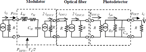
5.1.1. Direct modulation link diagram and definitions
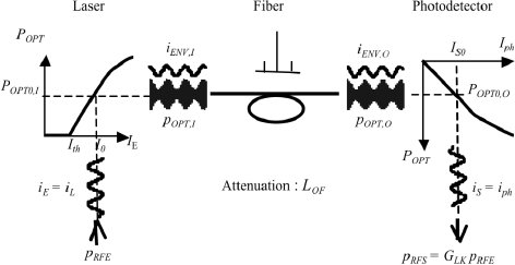
Figure 5.1 helps to define the principal parameters of a microwave photonic link with direct laser modulation without a command amplifier and without an amplifier after photodetection.
The laser is biased by an average current, I0, which determines the average optical power generation POPT0. The RF or microwave pRFE power applied at the input generates a peak alternating current in the laser, which has a peak amplitude iE. At the laser output this alternating current leads to amplitude modulation of the optical power with a power amplitude defined by a peak value pOPT,I. This is a double sideband modulation, as shown in Figure 5.1.
The modulated optical power (average power POPT,I and alternative amplitude power pOPT,I) is injected into an optical fiber where it undergoes an attenuation LOF. In the case of double sideband modulation, the chromatic dispersion of the fiber can induce an additional attenuation. The phenomenon will be examined in detail later. Similarly, the coupling between the laser and fiber in one part and the coupling between the fiber and photodetector in the other part are not perfect and hence introduce attenuations. For the moment, it will be considered that LOF regroups all these attenuations.
The modulated optical power is now injected into a photodetector. The continuous power POPT0,O component produces a continuous current, IS0, at the photodiode output, whereas the microwave modulation power, pOPT,O, produces an alternating current having a peak amplitude, iS. This current iS produces an RF or microwave power at the output:
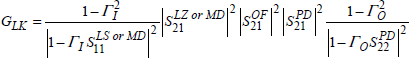
where GLK is the total gain of the link.
Figure 5.1. Parameters of a direct amplitude modulation microwave optical link (diagram of Figure 1.1). I and P are continuous amplitudes; i and p are peak amplitudes of alternating values
With these parameters, it is now possible to consider a fundamental concept in optical links: the relation between optical and electrical attenuation.
If the input microwave power, pRFE, is divided by four (−6 dB), the current applied to the laser is divided by two, which corresponds to an optical power divided by two (−3 dB). The photodetected current is, in turn, divided by two, corresponding to an output power divided by four (−6 dB).
In another way, an optical attenuation of 3 dB becomes an electrical attenuation of 6 dB or the fibers that attenuate 0.2 dB/km actually introduce an electrical attenuation of 0.4 dB/km.
Conversely, an optical gain of 10 dB becomes an electrical gain of 20 dB. This last remark explains the great benefit and success of optical amplifiers.
In Figure 5.1, the laser can be considered as an electrical-optical transducer and the photodetector can be considered as an optical-electrical transducer. The succession of these two transducers highlights another fundamental concept. If the optical power at a laser output is proportional to the current at laser input (nonlinear relation) and if the current detected by a photodetector is proportional to the optical power at the photodetector input (nonlinear relation), then the photodetected current is directly proportional to the current at the laser input (linear relation). Similarly, the photodetected electrical power is proportional to electrical power at the laser input (linear relation). Alternately, under normal conditions, it is two nonlinear relations inversed one from the other that produces a linear relation.
With the definitions above, the relation between small signal electrical and optical parameters can be detailed.
At the laser output:
[5.2] ![]()
where:
h is Planck’s constant;
q is electron charge;
v is optical frequency;
ηL is laser quantum efficiency;
iL is the current at laser input.
At the optical fiber output, the optical power was attenuated:
[5.3] ![]()
with:
– LOF = fiber losses including usual losses as a function of the optical wavelength and coupling losses but also the possible effects of chromatic dispersion;
– and:
![]()
where:
ωRF = microwave angular frequency;
L = fiber length;
vg = fiber group velocity.
Similarly, at the photodetector output:
[5.4] ![]()
where ηP is the photodiode quantum efficiency.
Another important definition concerns the optical wave modulation signal. Regarding the optical signal power variation, the majority of authors prefer to speak of optical signal envelope, such as that detected by a perfect photodetector. The current due to a photodetector with quantum efficiency ηP = 1 is thus spoken of. Laser diode envelope current is expressed as:
[5.5] ![]()
where iL is the laser input current.
Hence only envelope current is accounted for. Using equations [5.2], [5.3], and [5.4], the envelope current along the link is written:
[5.6] ![]()
[5.7] ![]()
[5.8] ![]()
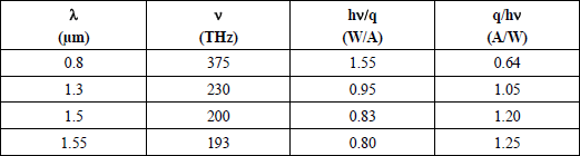
For example, Table 5.1 lists several example values for hv/q and q/hv as a function of light wavelengths.
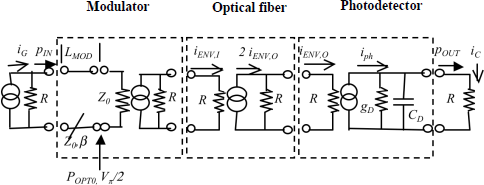
5.1.2. External modulation link diagram and definitions
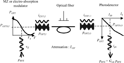
The diagram of Figure 5.2 shows an external modulation optical link (Figure 1.2). A light source (laser) inserts an optical power into a Mach-Zehnder or electro-absorption amplitude modulator. The modulator is biased by a voltage, V0, which determines an average output optical power, POPT0,I. Once the device is biased, it is controlled by a microwave power, pRFE, which means an alternating voltage having an amplitude, vE, across the control electrodes. This voltage modulates the optical power according to an amplitude pOPT,I. The relation between voltage vE and the amplitude of optical power is given by function f(vE) defined later:
The modulated optical power (double sideband) is injected into the optical fiber. From here, the optical power and its modulation follow the same steps as direct modulation. Equations giving pOPT,O and iph are the same as equations [5.3] and [5.4]:
It can also be considered that the optical power in the fiber is represented by the current detected by a perfect detector.
This leads to expressions below corresponding to parameters found in Figure 5.2.
Figure 5.2. Parameters of an external amplitude modulation microwave optical link (diagram of Figure 1.2). I and P are continuous amplitudes. i and p are peak amplitudes of alternative quantities
[5.12] ![]()
5.1.3. Simplified link diagram and first gain computation
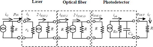
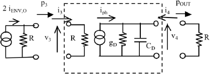
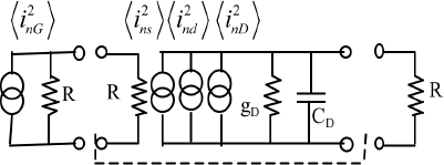
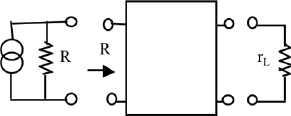
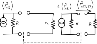
Figure 5.3 represents a simplified diagram of a direct modulation microwave optical link from the microwave signal viewpoint. As a result, only the optical signal envelope is considered. The source has an internal resistance R. The laser is simply represented by resistance rL. The modulated optical signal envelope at the laser output can be represented by an optical power peak amplitude pOPT,I or by an envelope of current detected by a perfect detector: iENV,I. At the optical fiber output, the power envelope is pOPT,O or the current envelope is iENV,O. The photodetector is represented by a conductance, gD, and a parallel capacitance, CD. The amplitude of the photodetected current is iph. This current generates a load current amplitude, iC. This load is the input of a transimpedance amplifier or of a receiver and for the moment, its resistance is R.
Figure 5.3. Simplified diagram of a direct modulation microwave photonic link
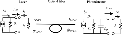
A computation from a similar diagram was presented in [FRI 02]. The peak current iG source has an internal resistance R.
The maximum power delivered by this source will be considered as the incidental microwave power of the optical link. It is given by the following equation where pIN is the maximum power available from the source:
from which current iG can be deduced:
Input current is given by:
Laser current is given by:
[5.18] ![]()
The amplitude of optical wave envelope currents and photodetected currents are defined by equations [5.5], [5.6], [5.7], and [5.8].
Load current iC is (to simplify computation: G = 1/R):
and output power (power delivered to the load) is:
[5.20] 
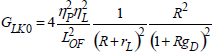
By introducing [5.4] to [5.8] and also [5.18] in [5.20], link gain, which is the transducer power gain, is obtained:
[5.21] 
From this expression, several remarks can be made:
– for a value of R = 50 Ω, a conductance gD of 1 mS and a capacitance CD of 0.2 pF, the cutoff frequency (frequency for which the gain is divided by two) of this gain is 16 GHz;
– when ![]() or when at low frequency or when the capacitance is compensated to a frequency point, for example, by an inductance, the link gain becomes:
or when at low frequency or when the capacitance is compensated to a frequency point, for example, by an inductance, the link gain becomes:
5.2. Optomicrowave S-parameters and gains of each photonic link component
5.2.1. Introduction
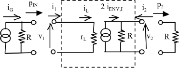
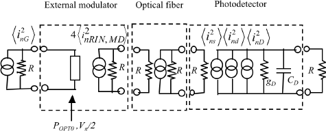
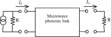
Knowledge of the overall amplitude behavior of a link is essential but it is also useful to know the contribution of each element in amplitude and phase. The useful signal being in microwaves, a good solution involves having access to S-parameters of each link part. The first stage consists of presenting the link in the form of component-level model boxes for the system-level simulations and for which input and output matching impedances can be defined. This is done in Figure 5.4.
Figure 5.4. Diagram of a direct modulation optical link showing component-level model boxes that can be defined by S-parameters
The laser output, the fiber input and output, as well as the photodiode input, have a resistance, R, in order to avoid all optical reflections. In reality, the laser output reflections affects its performance, but this is not yet taken into account in the models. The laser output, as well as the fiber output, has a current source 2iENV,I and 2iENV,O which induces envelope currents identical to those in Figure 5.3 at the optical fiber and photodiode inputs.
Each of these units is now defined by an input and output resistance, which allows the definition of laser, optical fiber, and photodiode optomicrowave S-parameters.
5.2.2. Optomicrowave laser S-parameters and optomicrowave gain
Starting with the laser unit, Y parameters from Figure 5.4 will be computed. This unit is detailed in Figure 5.5 and parameters Y11, Y12 and Y22 are defined by:
Parameter Y21 is defined by expression:
[5.24] ![]()
As for v2 = 0, (short-circuit output) by accounting for [5.12] and [5.18]:
[5.25] ![]()
Figure 5.5. Laser box diagram
and by combining equations [5.24] and [5.25]:
It is now possible to apply the equation in section 5.10.1 to calculate the laser box S-parameters by recalling that y = RY:
As for laser transducer gain, it becomes:
[5.31] 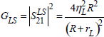
The laser model used above is very simplified. It is always possible to implement more complex linear laser models, which allow the computation of phase S21 and the laser relaxation frequency (Chapter 2).
5.2.3. Optomicrowave optical fiber S-parameters and optomicrowave gain
Microwave optical links can be used as delay lines [JAC 85] and for this, it is essential to know the fiber group time and corresponding phase. The current envelope relations (signal detected in a perfect photodetector) are:
Fiber S-parameters can be deduced:
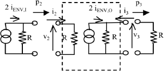
Optical fiber transducer gain is written:
5.2.4. Photodiode optomicrowave S-parameters and gain
It is also possible to establish photodiode S-parameters whose box diagram is given in Figure 5.7.
If the output is short-circuited:
from which the following can be extracted:
and directly:
Figure 5.7. Photodetectorbox diagram
from which the following parameters can be extracted:
Photodiode gain is written:
5.2.5. Localized component external modulator optomicrowave S-parameters and gain
As seen in more detail in Chapter 2 on external modulators, such a modulator is composed of electrodes placed on an electro-optic material. A voltage applied on these electrodes varies the refraction index of the material and, hence, the optical carrier phase. The phase combination in a Mach-Zehnder interferometer configuration allows the control and, hence, the modulation of the amplitude of the optical carrier via a microwave signal applied to the electrodes. If the electrode length is small in comparison to the microwave signal wavelength, it is a localized modulator. In this case, from the microwave input point, the electrodes can be represented by a capacitance.
If the electrode length is in the region of the microwave signal wavelength, the electrodes behave as a propagation line. This is a distributed external modulator whose performance shall be examined in the following paragraph.
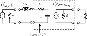
The electro-optic diagram of a localized modulator is represented in Figure 5.8. In this diagram, it is assumed that the modulator is used at a unique microwave frequency, allowing the neutralization of capacitance, CM, from the modulator by an inductance LM placed at the modulator input. This inductance corresponds to the real use of these modulators but also permits the simplification of computations.
The approach used corresponds to the approach developed in the laser section (5.2.2). Y parameters must first be computed, then the y normalized parameters, and finally, the S-parameters must be deduced from the equations given above.
Figure 5.8. Localized external modulator box diagram
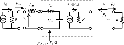
By recalling that for resonance angular frequency, ωRF0, inductance LM compensates the capacitance CM and by accounting for the material optomicrowave coupling, Y parameters for a modulator, biased at a voltage Vπ /2, and considered linear, are defined by expressions:
By recalling equation [2.71], the relation between ![]() (for short-circuit output) and v1 of Figure 5.8 is:
(for short-circuit output) and v1 of Figure 5.8 is:
where:
POPT0 represents continuous optical power at the modulator input;
Vπ is the modulator extinction voltage.
By recalling that y = R Y, it is now possible to apply the transposition expressions of Y parameters in S-parameters (section 5.10.1):
From these expressions, it is possible to deduce the modulator power transducer gain:
[5.50] ![]()
5.2.6. Distributed component external modulator optomicrowave S-parameters and gain
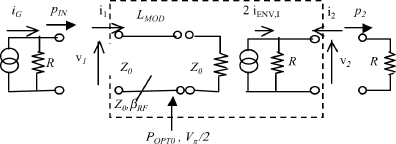
This time, the Mach-Zehnder modulator electrode lengths are in the region of the microwave wavelength, and these electrodes are considered as a propagation line. It is a distributed modulator type. This line shows the characteristics of a transmission line: characteristic impedance, Z0, a propagation constant, βRF, and a length, LMOD.
To ensure a constant voltage along the length of this line, it must finish in a matched load, Z0. Its diagram is represented in Figure 5.9. The continuous optical power at optical input is: POPT0 and the modulator is biased at an average voltage Vπ/2. Vπ is the modulator extinction voltage (equation [2.55]). The expressions below account for the material optomicrowave coupling. As long as it is a simplified diagram, the equivalent circuit of Figure 5.9 can also be used for an electro-absorption modulator.
Figure 5.9. Distributed externally modulated box diagram
The following step is the same as in the previous section. By considering the two-port network framed by dots in Figure 5.9, its Y parameters are evaluated first:
For the computation of Y21, it can be established that [FRI 02]:
with:
POPT0: continuous optical power at modulator input;
Ψ=βRF LMOD (nc-n)/2: phase difference between optical and electrical waves introduced along the propagation line;
![]() : propagation constant in the microwave modulator line;
: propagation constant in the microwave modulator line;
v: propagation velocity in the line;
LMOD: length of modulator line;
nc: modulator microwave line refraction index;
n: modulator optical guide refraction index.
and now:
Then by applying the transformations of Y-parameters to S-parameters (section 5.10.1):
The modulator transducer gain is written:
5.2.7. Summary of all S-parameters and optomicrowave gain
Table 5.2 summarizes the optomicrowave S-parameters of the different elements of localized or distributed, external or direct modulation microwave photonic links. It highlights both the propagated microwave signal amplitude and phase variations.
Table 5.2. Summary of link components S-parameters
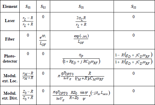
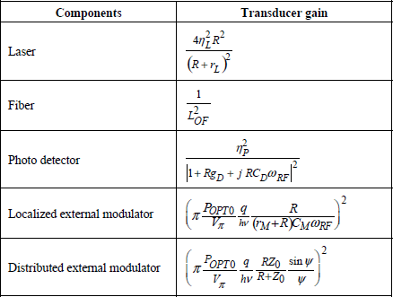
Table 5.3 summarizes optomicrowave gains of these same components. It establishes the transducer gain of a link as a function of its configuration and hence aids configuration choices.
Table 5.3. Summary of link components transducer gains
5.3. Microwave photonic links optomicrowave S-parameters and gains
5.3.1. Direct modulation microwave photonic link S-parameters
By accounting for the fact the boxes are matched between each other and that:
![]()
The S-parameters of the whole link can be written:
The S-parameters give access to the link amplitude and phase. From the amplitude of these S-parameters, different gains can be defined.
5.3.2. Direct modulation microwave photonic link gains
If the link input and output are directly connected to resistance R and in the measurement where: S12 = 0, it is the transducer gain which gives link gain:
[5.62] 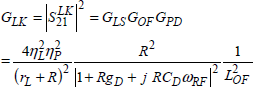
Obviously, this expression is identical to equation [5.21]. If the input is matched, it is the matched input transducer gain or power gain that gives the gain:
[5.63] 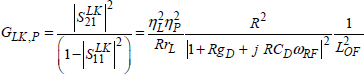
If the output is matched, it is the matched output transducer gain or available gain:
[5.64] 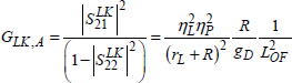
If the input and output are simultaneously matched, it is the maximum gain:
[5.65] 
5.3.3. Localized external modulator microwave photonic link S-parameters
Figure 5.10 represents the diagram of a localized external modulator microwave photonic link. As for a direct modulation link, the fact that the boxes are matched and that: ![]() is taken into account The S-parameters of the external modulation link are as follows:
is taken into account The S-parameters of the external modulation link are as follows:
Figure 5.10. Diagram of a localized external modulator microwave photonic link
As for a direct modulation link, the S-parameters give access to the link amplitude and phase. From the amplitude of these S-parameters, different gains can also be defined.
5.3.4. Localized external modulator microwave photonic link gains
These gains concerning a localized external modulation, have GLKXL type indices. If the link input and output are directly connected to a resistance, R, and in so far as S12 = 0, it is the transducer gain which gives the link gain:
[5.70] ![]()
If the input is matched, it is the matched input transducer gain orpower r gain:
If the output is matched, it is the matched output transducer gainor r available gain:
If the input and output are simultaneously matched, it is thmaximum um gain:
[5.73] ![]()
5.3.5. Distributed external modulator microwave photonic link S-parameters
Figure 5.11 represents the diagram of a distributed externamodulator or microwave photonic link. As for the direct modulation link, units that are matched can be accounted for and:
![]()
The S-parameters of the external modulation link are as follows:
Figure 5.11. Diagram of a distributed external modulator microwave photonic link
As for the direct modulation link, the S-parameters give access to the link amplitude and phase. From the amplitude of these S-parameters, different gains can also be defined.
5.3.6. Distributed external modulator microwave photonic link gains
To distinguish direct modulation gains, the gains have a GLKXD index type. If the link input and output are directly connected to resistance, R, and as so far: S12 = 0it is the transducer gain that gives the link gain:
[5.78] ![]()
If the input is matched, it is the transducer power gain with matched input or power gain:
If the output is matched, it is the transducer gain with matched output or available gain:
If the input and output are simultaneously matched, it is the maximum gain:
[5.81] ![]()
5.3.7. Link gain computation generalization
Generally where each link box is defined by its optomicrowave parameters, each box is subjected to R at the input and output, and the S12 parameters are zero, the link gain is given by the expression:
If the laser or modulator control amplifier has a different output impedance from R and the photodiode is connected to a receiver whose input resistance can also be different from R, for example RA as in Figure 5.12, then the expression giving the link gain becomes:
Figure 5.12. Link diagram with a laser, optical fiber, and photodiode
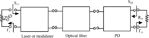
where:
Г1 is the reflection figure due to the amplifier output impedance amplifier ![]() ;
;
Г0 is the reflection coefficient due to load RA.
Figure 5.13 demonstrates the case where the link computation includes the input amplifier and a receiver or an output transimpedance amplifier. In this case, it is no longer possible to calculate the link gain from the products of |S21|2. The S’ parameters corresponding to the unit amplifier connection and laser unit must be computed first [GUP 81]:
But it should be noted there is no optical reflection in the laser. So ![]() and the expressions above become:
and the expressions above become:
Then the S’’ parameters corresponding to the photodiode box connection and the receiver box are computed. For this computation, ![]() is directly accounted for:
is directly accounted for:
Figure 5.13. Diagram of a microwave optical link with an amplifier and receiver
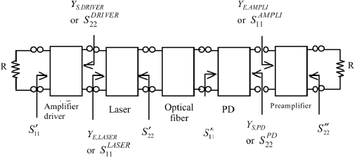
and the link gain becomes equal to:
5.4. Comparison of different link gains
5.4.1. Direct modulation link gain computation
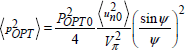
The first evaluation of direct modulation link gain can be done by taking the elemental values [FRI 02]: ηL = ηP = 1, R =1/G = 50 Ω, rL = 5 Ω, gD = 1 mS and zero losses: LOF = 1. The optical wavelength is 1.55 μm. The hypothesis also assumes ωRF is low. The gains can thus take different values as a function of input and output matching:
– if there is no input and output matching, transducer gain [5.62] must be used, giving a gain of 4.8 dB;
– if the input is matched and the output is directly coupled, the power gain [5.63] must be used, giving a gain of 9.6 dB;
– if the output is matched and the input is directly coupled, the available gain [5.64] must be used, giving a gain of 12.1 dB;
– if the input and output are simultaneously matched, the maximum gain [5.65] must be used, giving a gain of 17 dB.
If a resistance of 45 Ω is connected in series at the input and a second resistance of 52.6 Ω is connected in parallel at the output, showing a resistance of 50 Ω (resistive matching), the transducer gain must be used once again but with rL = 1/gD = 50 Ω. The gain is equal to -6 dB. This result shows the small benefit of this solution.
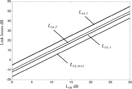
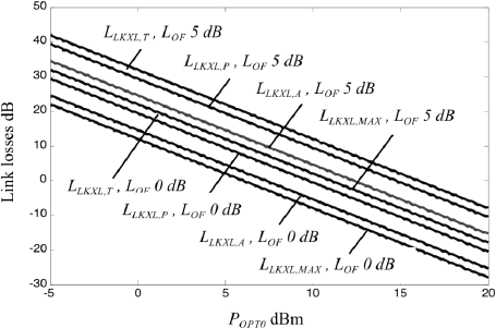
Figure 5.14 shows electrical losses (inverse of gain) in decibels as a function of the attenuation in the optical fiber for a direct modulation link obtained with the same values as above.
Several comments can be made regarding these curves:
– these curves clearly demonstrate that an optical attenuation variation of 10 dB turns into an electrical loss of 20 dB;
– the loss values for a zero attenuation fiber are negative in decibels for all gain types. It goes without saying that for a real link, the optical coupling between the laser and between the fiber in one part and the fiber and the photodetector in the other introduce optical losses of at least 5 dB, so 10 dB electrical losses. By waiting for the coupling improvements, the curves of Figure 5.14 must be read from an optical attenuation of 5 dB;
– on the curves, losses LLK,A and LLK,MAX correspond to an input and output matching, after the photodetector. This is only possible in the case of a fixed microwave frequency transmission and hence with a low bandwidth. In other cases, a wideband matching is not possible and output impedance in the order of 50 Ω after the photodetector is expected. The losses to consider are hence LLK,T and LLK,P.
Figure 5.14. Losses of a direct modulation link as a function of the optical loss
5.4.2. Localized external modulator link gain computation
The curves of Figure 5.15 are plotted from equations [5.70] and [5.73] for the following values: ηP = 1, CM = 20 pF, rM = 10 Ω, gD = 1 mS, CD = 1 pF, fRF = 100 MHz. The optical wavelength is 1.55 μm.
These curves show electrical losses are reduced as the square of applied optical power increase. It must be recalled that for this modulator, an inductance was placed at the input to compensate for the capacitance due to the electrodes. The input has a low resistance rM as it corresponds to the electrode losses and can be the object of matching. The curves describe the losses inverse to the transducer gain, power gain (input matching), available gain (output matching) and maximum gain (output and input matching). These losses are plotted for an optical attenuation of 0 dB and also for a more realistic value, the present state of optical connections, 5dB.
In Figure 5.15, losses without matching (transducer gain) with an optical attenuation of 0 dB and input and output matching losses (maximum gain) with an optical attenuation of 5 dB are merged. This shows it is possible to save 10 dB of electrical attenuation by adapting the link input and output impedances. This is possible with a localized modulator, generally used at low frequencies (100 MHz) and also with a low frequency band, facilitating this matching.
Figure 5.15. Electrical losses of a localized external modulator (Mach-Zehnder) link as a function of optical power at modulator input; the optical losses are 0 or 5 dB
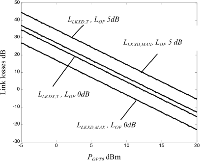
5.4.3. Distributed external modulator link gain computations
The loss curves of Figure 5.16 are plotted from equations [5.78] to [5.81] and are valid for a distributed Mach-Zehnder modulator. These curves are plotted for the following values: ηP = 1, gD = 1 mS, CD = 0.2 pF, fRF = 2 GHz. This has no relaxation frequency due to the very simplified laser model. Impedance Z0 of the modulator line is 50 Ω. As for Figure 5.15, these losses are plotted for an optical attenuation of 0 dB and also for a more realistic value of the actual state of optical connection, of 5 dB.
Equations [5.78] to [5.81] in section 5.4.2 show that electrical losses are reduced as a function of the square of applied optical power square. The losses have the same general appearance as in Figure 5.15, but as the input is matched, only losses LLKXD,T and LLKXLD,MAX are different.
It must also be noted that at high frequencies, wideband matching is often desired, which excludes the output impedance matching over the whole band. In these circumstances, it is not possible to attain the maximum link gain. For this reason a localized external modulation link matched for a narrow ban, has fewer losses than a distributed external modulation link.
Figure 5.16. Electrical losses of a distributed external modulation link (Mach-Zehnder) as a function of optical power at modulator input; the losses are 0 or 5 dB
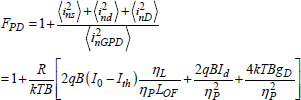
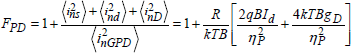
5.5. Direct modulation microwave photonic link optomicrowave noise figures
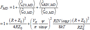
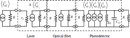
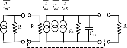
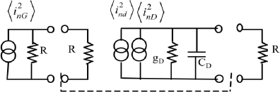
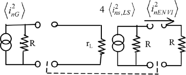
5.5.1. Link noise figure diagram and computation method
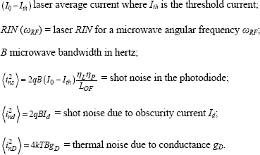
Figure 5.17 recalls the general diagram of a direct modulation link. The different noise sources are represented by random signal current sources, it will be assumed that they can be ordered between each other in the form of an average quadratic value sum. These currents are listed below:
[5.96] ![]()
with:
(I0 − Ith)is the average current in the laser where Ith is the threshold current;
RIN (ωRF)is laser RIN for a microwave angular frequency ωRF;
B is the microwave band width in Hz.
Figure 5.17. Direct modulation link diagram for noise figure computation
Section 5.10.2 recalls the steps leading to the choice of a microwave photonic link noise figure computation. The chosen method establishes the optomicrowave photonic link noise values for each link component, but the optical fiber is considered to have no noise. The Friis formula (see equation [5.103]) can thus be used as long as the value of fiber noise is FOF = 1.
The establishment of expressions giving the noise values of each component, and of the overall link for the simplified direct modulation microwave photonic link presented in Figure 5.17, corresponds to the computation presented in section 5.10.2.3.4. This computation will not be used here and only the results are considered.
5.5.2. Laser noise figure
The detailed evaluation of the noise figure is presented in section 5.10.2.3.1. It is carried out from the diagram presented in Figure 5.18.
Figure 5.18. Noises in the laser
The laser noise figure is defined by equation [5.147]:
[5.100] 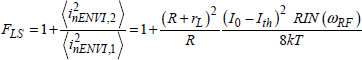
5.5.3. Optical fiber noise figure
As no noise is added to the fiber, the value of noise for the optical fiber is written:
5.5.4. Photodiode noise figure
The computation diagram for the value of photodiode noise figure is given in Figure 5.19. In this diagram, it is considered that thermal noise is applied by resistance R to the left of the input. However, resistance R to the right of the input is considered noiseless.
Figure 5.19. Noises in the photodiode
The resulting computation is defined by equation [5.151]:
5.5.5. Direct modulation link noise figure
The value of link noise figure is computed by using the Friis formula:
[5.103] ![]()
giving:
[5.104] 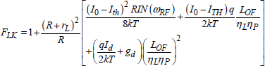
5.5.6. Matching effect at the input of a direct modulation link
As the laser input impedance is very low, it is possible to match the input. By doing this, the gain increases, as recalled in section 5.4.1 for the overall link, but at the same time, the noise figure diminishes. The diagram of Figure 5.20 symbolizes this matching by a purely reactive biport. The laser and link noise figure is given by equations [5.100] and [5.103] with laser transducer gain GLS; this gain must be replaced by the matched input laser gain. This gain is recalled below and values ![]() and
and ![]() can be found in Table 5.3.
can be found in Table 5.3.
Figure 5.20. Matching at laser input
[5.105] 
By introducing this new gain into [5.100] and [5.103], the new value of link noise figure is expressed as:
[5.106] 
The difference with equation [5.104] is the figure value of term 4rL. For R = 50 Ω and rL = 5 Ω, the ratio of the two terms is approximately 3. If the initial value of noise figure is considerably higher than 1, this introduces a very significant improvement to the value of the noise figure.
5.5.7. Generalization of a link noise figure computation
5.5.7.1. Laser, optical fiber, and photodiode link
This link is sketched in Figure 5.12. If the values of the noise figure and S21 optomicrowave parameters for each component are evaluated by an analytical computation or simulation, the value of the link noise figure can be deduced from equation [5.103].
NOTE:- This expression is the same regardless of the photodiode load resistance.
5.5.7.2. Link with driver and preamplifier
In this case, the reference diagram is that of Figure 5.13. The link noise figure becomes:
In this expression, the driver amplifier input resistance is always 50 Ω, so the circuit noise figure does not change. However, two term series are new. In one part FLS (YAD,O) and FPA (YPD,O) are the laser and preamplifier noise figures. They depend on the admittances presented at the input, in other words the amplifier and photodiode output admittances.
The new noise figure values can be evaluated by simulation and their variation can be considerable.
Elsewhere GAD,A and GPD,A, the amplifier and photodiode available gains (matched gain), equally vary with input and output matching. The figure for link noise figure will be as close as possible to the amplifier if it and preamplifier gains are high.
5.6. External modulation microwave photonic link optomicrowave noise figure
5.6.1. Equivalent diagram and steps recall
The steps followed to calculate external modulation microwave photonic link noise figure is validated in section 5.10.2 and previously used above. The diagram used for the link is that of Figure 5.21, in which the first box is that of the external modulator seen in sections 5.3.3 and 5.3.5 which can be localized or distributed.
Figure 5.21. External modulation link diagram for noise figure computation
It is hence necessary to determine the noise figure associated with the modulator optomicrowave, FMD. The link noise figure is then computed by using equation [5.103] in which FLS is replaced by FMD. Regarding the photodetector, the shot noise is now induced by the average optical power coming from the modulator. Its expression is different to that used in section 5.10.2.3.3. A new expression is established.
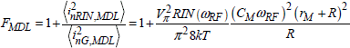
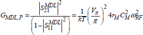
5.6.2. Localized external modulator noise figure
The equivalent diagram used for localized external modulator noise figure is that of Figure 5.22. The optical power applied at the modulator input is POPT0 and this modulator is biased at Vπ/2 in its linear operational zone.
Figure 5.22. Localized external modulator optomicrowave noise figure diagram
The output thermal noise due to the source is:
By introducing the expression of GMDL (see [5.50]):
Current at the modulator output due to laser RIN can be written (see [5.96] for the definitions):
and the localized external modulator noise figure can be written:
5.6.3. Distributed external modulator noise figure
The equivalent diagram used for noise evaluation is that of Figure 5.23. The optical power at the modulator input is always POPT0 and the modulator is biased at Vπ/2. However, the matching resistance Z0 of the LMOD line portion is itself a noise source.
Figure 5.23. Distributed external modulator optomicrowave noise figure diagram
The noise current entering the modulator due to resistance R is:
At the modulator output, the voltage due to this noise current is:
and the corresponding optical power is:
The square of the current at the modulator output due to input noise is:
Load Z0 at the end of the line, composed of the distributed electrodes, sends a noise power in the line of impedance Z0. At this line input, resistance R induces a reflection, introducing a standing wave on the line. As this line has a length of several wavelengths, the average line voltage along the line is regarded the same as in the case of matching. The expression obtained is a worst case as the propagation in the line is in the inverse direction of the optical wave, so the coupling is very weak. The noise contribution due to Z0 is hence:
With definitions identical to above, the current at the modulator output due to laser RIN can be written:
Giving the distributed modulator optomicrowave noise figure:
In this expression, if R = Z0, the second term is simply equal to 1 and the minimum value of the noise figure is 2 or 3 dB, recalling that this result is a worst case scenario.
5.6.4. New evaluation of photodetector noise figure
The computation is the same as that in section 5.5.4, but the shot noise term is a little different as the average optical power at modulator output is expressed differently. This computation is the same for the two types of external modulators. This term is now written:
from which the new equation for the evaluation of photodiode optomicrowave noise figure is:
5.6.5. Localized external modulator microwave photonic link noise figure
It is now possible to apply equation [5.103] but by accounting for the new link diagram:
[5.121] ![]()
Localized external modulator microwave photonic link noise figure is expressed as:
[5.122] 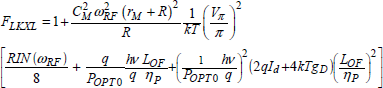
5.6.6. Matched input localized external modulator microwave photonic link noise figure
By following the same steps as in section 5.5.5, it is possible to calculate localized external modulator microwave photonic link noise figure when the input is matched. For this, the modulator gain, with matched input, must be computed by considering the S-parameters of Table 5.2:
Then the modulator noise figure (equations [5.103] and [5.105]) and, finally, the new link noise figure is computed (equation [5.121]):
[5.124] 
5.6.7. Distributed external modulator microwave photonic link noise figure
For a distributed external modulator, the following equation is applied:
[5.125] ![]()
from which the following equation can be produced:
[5.126] 
As it contains the term for distributed external modulator noise figure, it once again appears in the expression that for Z0 = R, the second term is equal to 1, which leads to a minimum noise figure of 2 (or 3 dB) for this link. It is also notable that the terms in brackets are identical to those of equation [5.124].
5.7. Comparisons of different link noise figures
5.7.1. Evaluation of direct modulation link noise figure
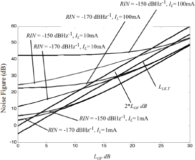
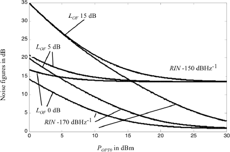
Evaluation of direct modulation link noise is computed with the same values of the link components as for the loss curves of Figure 5.14 and using equation [5.104], with optical losses in the fiber varying from 0 to 30 dB. Noise figure is computed for three “RIN-laser current” couples. The results are presented in Figure 5.24.
Several comments can be made:
– in this example, the values kept for the link elements are: rL = 5 Ω, gD = 1 mS, Id = 10 nA, R = 50 Ω. The RIN values are −150 and −170 dB/Hz, the current values IL = I0−Ithare 1, 10, and 100 mA;
– it must not be forgotten that in this present state, the laser-fiber and fiber-photodetector optical couplings introduce optical losses of at least 5 dB. The effect of these losses can be directly seen on the curves of Figure 5.24 by affecting the value of this optical loss (for example, 5 dB) for a fiber length of zero;
– the abscissa is optical losses. The relation between these losses and fiber length depends on the optical wavelength. The optical losses vary between 0.3 and 0.2 dB/km for wavelengths of 1.3 to 1.65 μm to which the coupling losses evoked above must be added;
– it is interesting to note that the plots depend on the biasing of the laser. For these high currents, the RIN then the “shot noise” term play an important role. For low currents, the noise figure also diminishes because of RIN and shot noise. As discussed in the following section, this also reduces the link dynamic range;
– it must also be noted that for low laser current values and high optical attenuations, the noise figure becomes inferior to electrical losses, whether expressed in the form of double the optical losses or even in the form of link losses (inverse of the gain). This very interesting phenomenon was confirmed by measurements carried out on real links [BIL 09];
– the above curves are given with a link that is not matched at the input or output. If a link with an optical loss of zero and with the input matched by a device without loss is considered, the link gain becomes the power gain and increases by 4.8 dB, whereas the noise figure (see the link between [5.104] and [5.106]), is reduced by 4.8 dB. This point is extremely important for the design of microwave photonic links.
Figure 5.24. Noise figure as a function of electrical losses of a direct modulation link
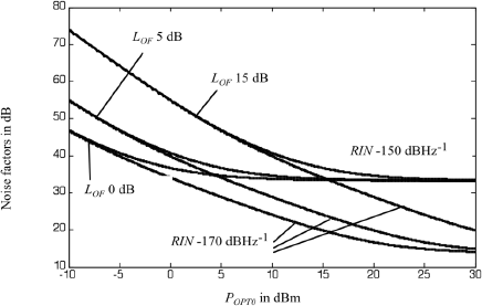
5.7.2. Evaluation of localized external modulator link noise figure
By using equation [5.122], it is possible to use the plots of Figure 5.25 to evaluate the noise figure produced by a localized external modulator link. These noise figures are given for three optical attenuation values (as indicated above, the value of 0 dB is not realistic) and for the two RIN values corresponding to a semiconductor laser (−150 dB/Hz) and a solid state laser (−170 dB/Hz). The values of the link elements taken for this plot are:
rM =5 Ω
CM = 10 pF
fRF = 100 MHz
Vπ =3 V
Id =10 nA
gD =1 mS
Figure 5.25. Noise figure for a localized external modulator link figure for two RIN values and three optical loss values LOF
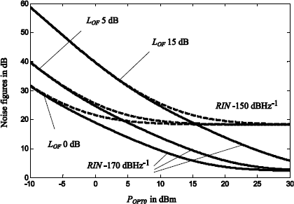
As for electrical losses, the noise figure is linked to the average optical power in the external modulator. In light of these curves, several remarks can be made:
– when the average optical power is sufficiently increased (it was applied up to 400 mW or 26 dB), the value of the link noise figure subsequently depends on laser RIN, which feeds the external modulator as shown by the noise figure as a function of Popt0, no matter the level of losses in the link;
– however, to obtain a low noise figure, a laser with a low RIN must be used. A RIN of 170 dB/Hz corresponds to a solid state laser, whereas a RIN of 150 dB/Hz corresponds to a semiconductor laser;
– to account for the optical loss due to coupling (minimum of 5 dB), the curves with LOF = 5 dB must be used;
– the results below must be refined by accounting for the fact that, in one part, the RIN varies considerably with the microwave frequency and also, the laser RIN tends to decrease when the optical power increases.
5.7.3. Evaluation of matched input localized external modulator link noise figure
The results of Figure 5.25 can be further improved by accounting for evaluating the matched input noise (equation [5.124]). This is presented in Figure 5.26 where the applied optical power values have been restricted to better show the possible minimum noise figures.
Figure 5.26. Noise figures for input matched localized external modulator links for two RIN values and three optical loss values LOF
5.7.4. Evaluation of distributed external modulator link noise figures
By using equation [5.126], it is possible to establish the curves giving external modulator link noise.
As for electrical losses, the noise figure is linked to the average optical power of the external modulator. For the same component values, Figure 5.27 gives a noise figure example as a function of the optical power at a Mach-Zehnder modulator input. In light of these plots several remarks can be made:
– when the average optical power is sufficiently increased, the link noise figure depends on the laser RIN, which feeds the external modulator;
– however, to obtain a low noise figure, a laser with a very low RIN must be used. This RIN (−170 dB/Hz) is only possible with solid state lasers;
– to account for optical losses due to coupling (minimum of 5 dB), the two curves with LOF =5 dB are to be used.
Figure 5.27. Evaluation of distributed external modulator link noise figure for two RIN values and three values of optical loss LOF
Equation [5.125] is composed of three terms. The first term is the modulator noise figure FMDD due to RIN, the second term is zero, and the third term is partly composed of shot noise named NF1 and partly thermal noise induced by gD named NF2, (with the values above, obscurity noise is negligible). From equation [5.126], it is possible to see the influence of each of these terms on the noise figure of an external modulation link. This is represented in Figure 5.28 for an RIN of -170dB/Hz.
Figure 5.28. Different noise components of a distributed external modulator for a RIN of -170 dB/Hz and two values optical loss LOF
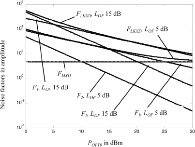
In this figure, it appears the modulator noise figure is constant as a function of optical power and, obviously, does not depend on optical losses. The gD (F2) thermal noise is predominant only for low applied optical powers (POPT0). For high optical powers, it is sometimes RIN (5 dB LOF) and sometimes shot noise (15 dB LOF) that prevails.
5.7.5. Output noise power
Expressions giving link gain and noise figures allow the estimation of noise at the link output. For a direct modulation link, power NS is given by the expression below:
where GLK and FLK are given for a direct link by equation [5.62] and [5.104].
For another link type (external modulation), the gain and noise figure are replaced by corresponding expressions. When measuring the noise of an optical link, the noise in the output resistance can add itself to the link noise. The noise in this resistance must then be estimated.
Figure 5.29 can help to make this estimation. The noise power, in the output resistance R, is defined as follows:
Figure 5.29. Diagram of a direct modulation link output noise powers
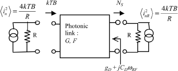
Figure 5.30. Direct modulation link output noise powers
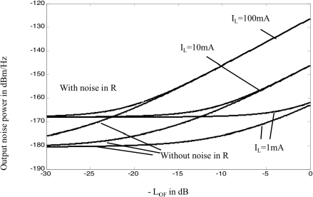
Total output noise is given by the sum of the two preceding noises. However, if an amplifier with a high gain and a low noise is placed at the output, the noise in resistance R behind the amplifier becomes negligible and, in this case, the output noise no longer includes the load resistance noise. This leads to two different output noise evaluations as represented in Figure 5.30, where the output noise is evaluated in the same direct modulation link as for Figure 5.24, for three laser biased currents. Output noise is evaluated in decibel per hertz as a function of the inverse of fiber losses (−LOF in dB) with and without noise in the output resistance. It is important to note that for the plots of Figure 5.30, the RIN noise is considered constant.
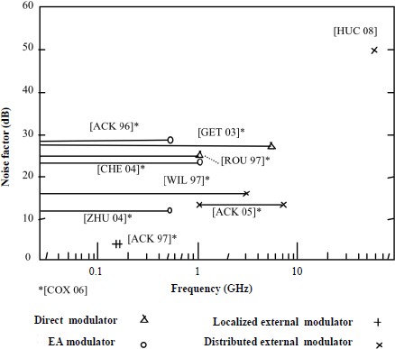
5.7.6. Some effectively measured noise figure values
Numerous results of the evaluation of microwave photonic link noise figure have been published. Figure 5.31 gives an outline of development in this domain. In this figure, a first series of results (the references with an asterisk are from [COX 06]) show different microwave photonic link noise figures below 10 GHz which can transmit digital signals at several megabits per second. These link modulations are carried out either externally or directly. In external modulation, localized or distributed Mach-Zehnder and electro-absorption modulators appear. In these results, a very low link noise figure is shown, which is due to matching at the modulator input [ACK 97].
Another photonic link type appears now. It is intended to serve as an extension to 60 GHz microwave links. A link example in which the authors have reported the optical noise power is presented in Figure 5.31 [HUC 08]. Due to the microwave frequency, the noise figure of these links is higher but these links enter into another category as they are intended to transmit signals at rates in the order of gigabits per second.
In this category, several optical links are proposed in systems composed of microwave links including a 60 GHz microwave carrier. These links are intended to transmit digital signals, the link quality is found by measuring the bit error rate (BER) or the error vector magnitude (EVM) of the transmitted digital signal. This evaluation includes the microwave link, which is the most penalizing and generally does not allow the separation of photonic link effects. For a frequency of 60 GHz, it shall be shown in Chapters 6 and 8 (Figure 8.7) that with a double sideband modulation, the signal completely disappears over a distance of 1 km. So with this modulation, the fiber length cannot be larger than a few hundred meters.
Figure 5.31. Examples of microwave photonic link noise figure
To counter this phenomenon, one of the sidebands or carriers must be removed. All 60 GHz systems have optical carrier suppression by using an external modulator biased at Vπ (see section 6.2.3) or a unique sideband transmission through the suppression of one of the two sidebands by optical filtering. These systems are all based on 1.55 μm wavelengths. Some examples of these links are demonstrated later. In all these examples, the wireless link is at 60 GHz.
A first realization allows the transmission of a 156 Mb/s signal in an 85 km fiber and a wireless link of 5 m [KUR 99]. Another achievement was the transmission of a 155 Mb/s signal over a 25 km fiber and a 2.6 m wireless link [KIM 04]. Another link transmitted 37 high-definition television channels 27 Mb/s each, or 1 Gb/s in total over a 20 km fiber and a 4 m wireless link [CHU 07]. In these examples, the effect of the photonic link on noise figure and dynamic range from the wireless part. This is why they are not presented on Figure 5.3.1.
The example given in Figure 5.31 transmits a 1 Gb/s signal over a 50 m fiber and a 15 m wireless link [HUC 08]. Finally, a signal of 15.5 Gb/s was transmitted over a 50 m erbium-doped optical fiber and a 3.1 m wireless link [WEI 08].
5.8. Microwave photonic link nonlinearity: distortion phenomena
5.8.1. Single microwave signal nonlinearity
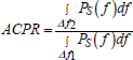
Knowing the value of link noise figure and saturation levels, it is possible to deduce the dynamic range. The first expression of saturation (output signal nonlinearity) appears when a single signal is applied to the link. The signal response is no longer proportional to the amplitude of the signal applied at the input. This behavior is similar to all analog responses in electronic circuits, such as amplifiers. The subset response is characterized by a curve, such as that represented in Figure 5.32. It appears an output saturation signal can be quantified by an output power level for a compression of 1 or 3 dB (systems composed of a constant envelope modulation) or for a compression of 0.1 dB (systems simultaneously transmitting numerous channels). In Figure 5.32, these levels are found by ps1dB or ps0.1dB values.
Figure 5.32. Microwave photonic link nonlinear response with a single input frequency
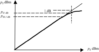
Outside of complex linearization techniques used for photonic links, another method consists of applying a reduction based on the experiment and not exceeding a certain input level signal so as to not induce a compression superior to that desired, e.g. 0.1 dB or 1 dB.
Figure 5.33. Diagram of second harmonic effect as long as the system bandwidth is inferior or superior to 2F0
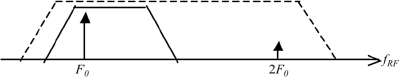
In addition to the fundamental frequency distortion, nonlinearity can introduce harmonics. If the signal bandwidth is inferior to the octave, the signal of the second harmonic is outside the band and eliminated. However, if the signal bandwidth is superior to the octave (fiber optic transmission of a ultra-wideband (UWB) signal within the 3.1-10.6 GHz band or high-bitrate communications: 12, 40, or 80 Gb/s) the signal upon the second harmonic must be accounted for and even upon the third harmonic. This is shown in Figure 5.33.
5.8.2. Several input microwave signals nonlinearity
In the case of several microwave signals at the system input, intermodulations appear, potentially creating undesirable interference. To prevent cumbersome terms, these microwave signals shall be called f1, f2 or 2f1,2f2 instead of fRF1, fRF2 or 2 fRF1,2 fRF2.
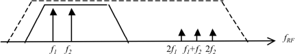
The first intermodulation is second order. In this case, the interference is around the second harmonic of the two input signals and the amplitude of their disruption depends on the system bandwidth as above. This is schematized in Figure 5.34.
Figure 5.34. Schematization of the second harmonic effect according to the inferior or superior system bandwidth at 2f2 in the case of two input signals
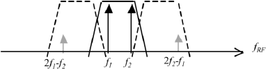
The second intermodulation is third order. This time, interference signals appear in proximity to the applied input signals. Figure 5.35 schematizes these in the case of an operation with several channels. This diagram shows in this configuration, the signals distort the adjacent channels. In all cases the capability of imposing an amplitude limit is necessary.
Figure 5.35. Schematization of the third-order intermodulation effect in the case of two input signals
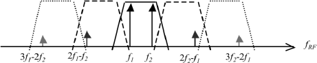
The third intermodulation to take into account is the fifth-order intermodulation. Again, interference signals appear in proximity to the applied signal frequencies and these interferences must be controlled. This is schematized in Figure 5.36.
Figure 5.36. Schematization of third and fifth-order intermodulation effects in the case of two input signals
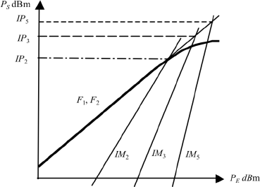
These intermodulation signals give rise to interference signals with amplitudes comparable to the signal amplitude of the fundamental frequency.
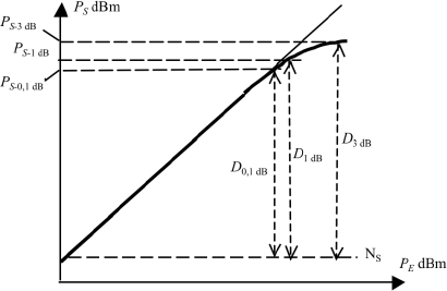
This is schematized in Figure 5.37 where the different intermodulation signals described above are represented as well as the corresponding second, third, and fifth-order interception points, which define the intermodulation level for a given system.
Figure 5.37. Second, third, and fifth-order intermodulations and corresponding interception points
5.8.3. Wideband input signal nonlinearity
If the input signals are no longer defined by one or several unique frequencies but by a spectrum in a given band (channel), the third and fifth-order intermodulations appear as in Figure 5.38 [CRI 99].
Figure 5.38. Non-sinusoidal signal intermodulation spectrum
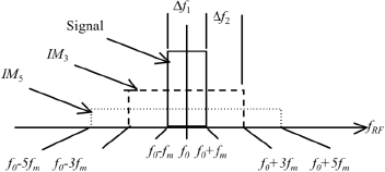
In this figure, the signal part appears as a microwave signal modulation in a 2fm frequency band around a central frequency, fRF, called f0 for simplification, and which defines a transmission channel.
Recalling in this case, the intermodulation, e.g. third order, is defined as a ratio between the adjacent channel power and the power in the signal band called adjacent channel power ratio or ACPR defined by:
5.8.4. Nonlinearity combination of microwave photonic link components
To summarize, each of the microwave photonic link components is able to generate interference signals corresponding to the different intermodulations described above. These signals then combine to give intermodulation levels of the whole link. Depending on the signals combining in phase or not, the final result will be different and only a complete simulation produces an accurate result. It is nonetheless possible to have the worst case of these combinations (combination in phase) as a result of the following equation giving the n order interception points of a link composed of m components [MAA 88; MAA 95]:
[5.130] ![]()
where:
IPn,M is the n order interception point of unit M;
GM is the unit M gain.
With equation [5.130], it is possible to calculate the second, third, or fifth-order interception points. For example, the interception point for a third-order (n = 3) intermodulation for a link composed of three units (M = 3), the expression above becomes:
In the present state of the models, the interception points of all link components are given by corresponding nonlinear model simulations.
5.9. Microwave photonic link interference-free dynamic range
5.9.1. Single input signal microwave photonic link interference-free dynamic range
In the case of a single input frequency (distribution of a reference signal), there is no intermodulation and only a signal compression. The maximum acceptable signal is only limited by the maximum compression rate. Even with a unique signal, there can be link linearity constraints.
A compression point of 0.1 dB guarantees good linearity. A compression point of 1 dB corresponds to an acceptable value, e.g. phased-array antennas. Finally, certain “constant envelope” telecommunication protocols can have 3 dB compression points. The minimum authorized signal is the noise floor (Ns in Figure 5.39).
Figure 5.39. Single input signal link dynamic range
This noise floor is expressed in decibels referenced to 1 milliwatt (dBm) in a 1 MHz band:
with GLK, FLK in decibels.
It is thus possible to express a compression point-dependent dynamic range given by the expressions below for the three compression points in Figure 5.37:
In these expressions:
![]()
B in megahertz;
GLK, FLK in decibels.
In these expressions, another manner of interpreting the dynamic range is to consider it as a maximum signal to noise (S/N) ratio. It goes without saying that the dynamic range deduced for a given S/N ratio is much lower.
5.9.2. Several-input signal microwave photonic link interference-free dynamic range
According to the steps recalled in section 5.10.2, it is possible to extract the second, third, or fifth-order interference-free dynamic ranges. These dynamic ranges are given by the expression below and are schematized in Figure 5.40:
In these expressions:
IP2, IP3, IP5 in dBm
−114=10log(kT106)+30 in dBm
B in MHz
GLK, FLK in dB
Figure 5.40. Two input signal link second, third, and fifth-order dynamic ranges
Several remarks can be made from these equations and Figure 5.40:
– as for the dynamic ranges with a single input signal, the noise floor of Figure 5.40 involves a S/N ratio of 0 dB. If the S/N ratio must be superior, the dynamic range becomes reduced;
– in the expressions corresponding to second, third, or fifth-order interference-free dynamic ranges, the frequency powers are 1/2, 2/3, or 4/5. This must be accounted for when comparing the dynamic ranges of different bandwidths;
– concerning second-order intermodulation, recalling that it is simply the second signal harmonic and this is of concern only for systems with bandwidths larger than one octave;
– Figure 5.40 shows how dynamic ranges D2, D3,or D5 can be indiscriminately read on the input power (PE) or output power (PS) axes;
– when the fifth-order dynamic range is considered, it is assumed that the third-order intermodulation is eliminated (system linearization). In this case, frequencies f1and f2 are less compressed than on Figure 5.40.
5.9.3. Some effectively measured interference-free dynamic range values
A remarkable collection of results was carried out in [COX 06] and numerous interference-free dynamic range examples are presented within. The modulations are classified into direct modulation and narrow or wideband band external modulation (inferior to the octave). The corresponding dynamic ranges are third-order dynamic ranges. The external modulators can also be linearized (this technique involving several external modulators is described in [COX 04]). In this case, the third-order intermodulation is attenuated and the induced dynamic range is a fifth-order dynamic range. All the presented dynamic ranges are for 1 Hz.
A first group of results are between 0.1 and 1 GHz. The direct modulation and wideband external modulation give a dynamic range of 120 dB/Hz2/3. The linearized wideband external modulations give 122 dB/Hz4/5 and linearized wideband external modulators attain a dynamic range of 130 dB/Hz4/5.
These dynamic ranges then decrease down to 10 GHz. So, the direct modulation has a dynamic range of 100 dB/Hz2/3, the wideband external modulators have a dynamic range of 105 dB/Hz2/3, and the narrowband external modulators have a dynamic range of 110 dB/Hz2/3. Linearized narrowband external modulators offer a dynamic range from 120 to 125 dB/Hz4/5.
For 60 GHz links, the dynamic range is included in the bit error rate (BER) on the transmitted digital signal and even in this case the microwave wireless component of the link weighs more than the optical fiber component.
5.10. Appendix
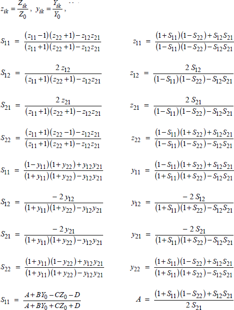
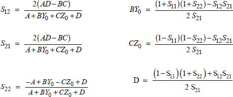
5.10.1. Relation between parameters S, Z, Y, and ABCD
The expressions below give the cross-relations between parameters S, Y, Z, and ABCD of a two-port network:
5.10.2. Equation choice for the computation of microwave photonic link optomicrowave noise figure
5.10.2.1. Possible evaluation methods for link noise
The evaluation of microwave photonic link noise figure is confronted by several questions:
– is the value of the noise figure of the link at least equal to the optical loss LOF or electrical loss, ![]() ?
?
– Is the computation method for the noise figure the same in the optical domain and the microwave domain?
– What is the contribution of each link component to the value of overall link noise figure?
– Is there the possibility of computing the noise figure values for each link component and combine them via the Friis expression?
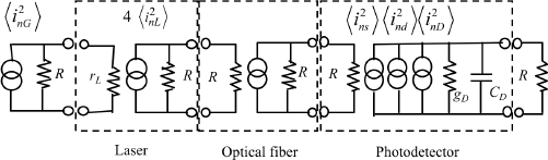
In order to answer these questions developments presented in this section were detailed by [BDE 08]. By using the diagram from Figure 5.4, it is possible to add to it noise sources (current variances) corresponding to thermal noises due to resistances from the source and photodiode, laser RIN, and shot noises due to the optical power and obscurity current of the photodiode (Figure 5.17). In this list, the possible polarization noises due to the optical fiber are discounted. This diagram is presented in Figure 5.41.
Figure 5.41. Noise figure computation link diagram
In this diagram, the different sources are represented by random signals presented in section 5.5.1, but which are recalled below for the clarity:
with:
NOTE:- The RIN definition used to define current ![]() above is taken from equation [5.96] and hence introduces a 1/2 figure that does not feature in [BDE 08]. This changes nothing to the demonstration below.
above is taken from equation [5.96] and hence introduces a 1/2 figure that does not feature in [BDE 08]. This changes nothing to the demonstration below.
From this diagram and noise sources, one method of evaluation consists of directly calculating the overall link noise figure. This computation was performed in [FRI 02; BDE 08] and is not presented here.
Another method consists of separately calculating the noise figures of each component of Figure 5.41 and combining them to obtain the overall noise figure. However, one part of the link is electric and another is optical, raising questions on the computation steps. In the following, an analysis is proposed which is derived from the microwave domain and this analysis will be compared to that used in optoelectronic domain. It will be demonstrated that they lead to the same results.
A first computation to obtain the contribution of each component consists of defining the optomicrowave noise figures and assuming that no noise comes from the optical fiber. This leads to the fact that the Friis formula can be used to calculate overall values of link noise figure.
To obtain the noise figures of each component, a second calculation can be performed by using a step used in the optoelectronic domain, and a characteristic example is given in [BAN 00]. This step consists of separately accounting for the shot noise effect in the optical fiber (the optical fiber shows a noise figure equal to optical losses) and the other noise sources by computing the noise figures of each element. Unfortunately, in this case, the overall noise figure cannot be obtained by combining the noise figures of each unit according to the Friis formula.
This second calculation gives an identical value of overall noise to that obtained by the first calculation. These two calculations are themselves identical to the overall noise figure calculation, not performed here but presented in [FRI 02; BDE 08]. This hence shows that the first method proposed is valid.
5.10.2.2. Recall of the noise figure calculation of a two-port network
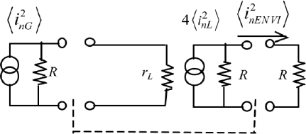
To calculate the noise figure, the noise sources can be taken back to input, output, or to the two-port network interior. The choice is only guided by the difficulty of the calculation. The second or third method is chosen as a function of the link components.
The parameters corresponding to the second method are represented in Figure 5.42 showing a two-port network, the noise of which is characterized by an output current source ![]() . It is fed by a source of resistance R, characterized by a current source with a mean squared value
. It is fed by a source of resistance R, characterized by a current source with a mean squared value ![]() and a power of 4 kTB. The incident power at the two-port network input is kTB and the output power is GTkTB with GT, transducer gain of this two-port network.
and a power of 4 kTB. The incident power at the two-port network input is kTB and the output power is GTkTB with GT, transducer gain of this two-port network.
The corresponding output current is:
Figure 5.42. Noises in the two-port network reported at the output
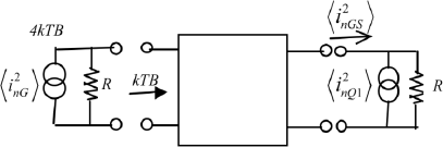
In these conditions, the two-port network noise figure is given by:
The same method is used to calculate the values of laser and modulator noise figures.
Another solution consists of restoring all the noise sources into the two-port network as in Figure 5.43. In this case, the current sources corresponding to the noises are placed before the admittance output Y of the two-port network. The squared current corresponding to the input thermal noise is hence expressed:
Figure 5.43. Noise placed just before the two-port network output admittance
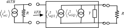
This time the noise figure is expressed as:
It is this expression that is used for calculation of photodetector noise figure.
5.10.2.3. First calculation of link noise figure
This step consists of considering that the shot noise appears in the photodiode and that in this case, the optical fiber does not introduce noise. In these conditions, the calculation of noise figure for each component is detailed below.
5.10.2.3.1. Laser noise figure
The appropriate diagram is that of Figure 5.44. In this diagram, the output resistance is considered noiseless. The current at the laser box output is composed of a term due to the input thermal noise and of a term due to RIN:
The available noise power in source resistance R is 4 kTB and the laser incident noise power is kTB. At the output, the noise in load R is expressed ![]() . It can hence be written according to expression [5.31] and by taking GLS as the laser gain:
. It can hence be written according to expression [5.31] and by taking GLS as the laser gain:
The following can be extracted:
Laser noise can be written:
The laser noise figure is hence written:
[5.147] 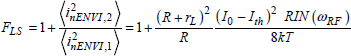
Figure 5.44. Laser noise
5.10.2.3.2. Optical fiber noise figure
As no noise is added in the fiber itself its noise figure is written:
5.10.2.3.3. Photodiode noise figure
The diagram for the calculation of photodiode noise figure is given in Figure 5.45. In this diagram, it is assumed that a thermal noise is applied by resistance R to the left of the input. However, resistance R to the right of the input is assumed to be noiseless. At the photodiode input, the current due to thermal noise in R is expressed:
and in the photodiode circuit:
Figure 5.45. Photodiode noise in the first computation
For the shot noise, the obscurity current noise and thermal noise due to gD, the values are given by expressions at the beginning of section 5.10.2.1. The photodiode noise figure can hence be expressed:
[5.151] 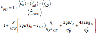
5.10.2.3.4. First expression of link noise figure
Now, the calculation of link noise figure can be undertaken using the Friis formula:
[5.152] ![]()
With FOF = 1, gives:
[5.153] 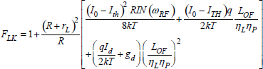
This result is to be compared to that obtained with the analysis of the next section which is commonly used in optoelectronics.
5.10.2.4. Second calculation of link noise figure
5.10.2.4.1. Presentation of the second calculation
This analysis, taken from the procedure used in [BAN 00], consists of calculating noise figure for each link component, as well as obscurity and thermal noises in the photodiode. The combination of these noise figures by the Friis formula gives a first link noise figure. As this is done in optoelectronics, shot noise is considered separately. A noise figure specific to shot noise is calculated for the laser, for the optical fiber, and for the photodiode. However, for these calculations, it is the definition of optical noise figures which are considered, in other words at each component output, only the excess noise is accounted for. Thus the link shot noise figure can be computed and associated to the previous. This time, the association cannot be performed by the Friis formula, preventing its wide use.
5.10.2.4.2. Laser noise figure
This calculation is the same as that given by equation [5.147].
5.10.2.4.3. Photodiode noise figure
The diagram for the calculation of photodiode noise is given in Figure 5.46. In this diagram, it is considered that a thermal noise is applied by resistance R situated to the left of the input. However, resistance R situated to the right of the input is considered as noiseless. At the photodiode input, the current due to thermal noise in R is expressed:
Figure 5.46. Photodiode noise in the second computation
and in the photodiode circuit:
For the obscurity noise current and the thermal noise due to gD, the values are given by expressions at the beginning of section 5.10.2.1. The photodiode noise figure can thus be expressed:
5.10.2.4.4. First part of the laser and photodiode noise figures
The combination of equations [5.147] and [5.152] by the Friis formula for the three components: laser, optical fiber (FOF = 1), and photodiode gives:
[5.158] 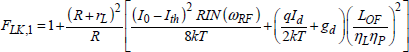
5.10.2.4.5. Noise figure due to shot noise
The calculation of noise figure is performed by the input signal to noise power ratio divided by the output signal to noise power ratio by assuming that thermal noise occurs at the input and shot noise occurs at the output.
Laser (shot) noise figure
The parameters evoked correspond to Figure 5.47. Between the input and output, the current square value is simply multiplied by ![]() .
.
The input noise is:
![]()
and at the output:
![]()
where noise figure is expressed as:
Figure 5.47. Shot noise at laser output
Optical fiber (shot) noise figure
With the same steps as above, it is found that:
For shot noise, and only for this noise, the fiber noise figure is equal to its optical loss.
Photodiode (shot) noise figure
Similarly, the noise figure between the photodiode input and the photodiode noise current is:
The shot noise part of the link noise figure:
[5.162] ![]()
It is noted that this noise figure is no longer obtained with the Friis formula.
5.10.2.4.6. Second expression of link noise figure
The combination of the two noise figures of equations [5.158] and [5.162], is simply obtained by adding them. The resultant noise figure is hence written:
This noise figure is identical to that obtained in equation [5.153], showing that the two analysis converge.
5.10.3. Calculation of a two-input signal microwave photonic link interference-free dynamic range
5.10.3.1. Introduction
The computations below are not specific to a microwave photonic link and are classical enough for third-order intermodulation [HA 81]. However, they are much less common for second and fifth orders. It is hence useful to remember these calculations to know where powers 1/2, 2/3 or 4/5 come from for the frequencies.
An electrical current IE is applied at the input of the link defined in Figure 5.48.
Figure 5.48. Parameters in a microwave photonic link
In the expressions below, the electrical angular frequencies considered are ω1 and ω2. If the input is composed of two identical amplitude signals, IE can be written:
[5.164] ![]()
The output current is IS. To show the second, third, and fifth-order nonlinearity, the relation between IE and Is develops in a Taylor series:
[5.165] ![]()
5.10.3.2. Third-order intermodulation interference-free dynamic range
By combining the two equations [5.164] and [5.165] and neglecting the fifth order terms, the output current is composed, amongst others, of ω1, ω2, (2 ω1 − ω2) and (2 ω2 − ω1) terms. By only considering the term with these variables, current IS is expressed:
Referring to Figure 5.49, the different powers in dBm dissipated by current IS in output resistance R can be established:
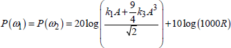
[5.168] ![]()
[5.169] 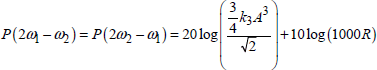
Figure 5.49. Output power of a third-order intermodulation microwave photonic link
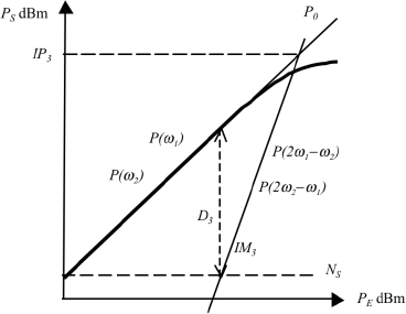
The third-order interception point is obtained by equaling powers P0 and P(2ω1− ω 2) or P(2 ω2− ω1):
[5.170] ![]()
By combining equations [5.168], [5.169], and [5.170] the following can be written:
For the low intermodulation levels considered, the approximation below can be made:
[5.172] ![]()
giving:
The dynamic range is thus defined by an acceptable intermodulation level P(2ω1− ω2), defining a maximum power P(ω1):
However, the acceptable interference level is fixed by the noise level NS at the link output in a frequency band B. This noise is expressed as:
with B in megahertz and k = Boltzmann constant.
Whereas the interference-free dynamic range due to the third-order intermodulation is written:
In this expression D3 is expressed in dB/MHz2/3. The ratio between the link dynamic range with a bandwidth of 100 MHz and a dynamic range corresponding to a bandwidth of 1 GHz is 4.6 in amplitude and 6.6 in dB.
5.10.3.3. Fifth-order intermodulation interference-free dynamic range
This time, by combining the two equations [5.164] and [5.165], the output current is composed amongst others of terms in ω1, ω2, (3ω1 − 2ω2) and (3ω2 − 2ω1). By only considering the terms containing these variables, current IS is expressed:
The fifth-order interception point is obtained by equaling powers P0 and P(3ω1−2 ω2) or P(3 ω2−2 ω1):
With approximation [5.172], the following can be written:
This allows the fifth-order interference-free dynamic range expression for a given intermodulation power:
and by writing that the intermodulation level must not be greater than the noise level the following is true:
This time, D5 is expressed in dB/MHz4/5. The ratio between a link dynamic range with a bandwidth of 100 MHz and a dynamic range corresponding to a bandwidth of 1 GHz is 6.3 in amplitude and 8 in dB.
5.10.3.4. Second-order intermodulation interference-free dynamic range
This time it is no longer truly an intermodulation, as now the frequency considered is on the second harmonic. By combining the two equations [5.164] and [5.165] in which the terms above IE2 are neglected, the output current is composed, amongst others, of terms in ω1, ω2, 2 ω1 and 2 ω2.
By considering the terms containing these variables, current IS is expressed:
from where the following can be deduced by equaling the power on the fundamental and second harmonic:
from where the expression:
giving the second-order dynamic range:
This time D2 is expressed in dB/MHz1/2. The connection between a link dynamic range with a bandwidth of 100 MHz and a dynamic range with a bandwidth of 1 GHz is 3.16 in amplitude and 5 in dB.