INSTRUCTION CYCLE TIMINGS
D.1. USING THE INSTRUCTION CYCLE TIMING TABLES
D.2. ARM7TDMI INSTRUCTION CYCLE TIMINGS
D.3. ARM9TDMI INSTRUCTION CYCLE TIMINGS
D.4. STRONGARM! INSTRUCTION CYCLE TIMINGS
D.5. ARM9E INSTRUCTION CYCLE TIMINGS
D.6. ARM10E INSTRUCTION CYCLE TIMINGS
This appendix lists the instruction cycle timings for some common ARM implementions. Timings can vary between different revisions of an implementation and are also affected by external events such as interrupts, memory speed, and cache misses. You should treat these numbers as a guide only and verify performance measurements on real hardware. Refer to the manufacturer’s data sheets for the latest timing information.
ARM cores use pipelined implementations. The number of cycles that an instruction takes may depend on the previous and following instructions. When you optimize code, you need to be aware of these interactions, described in the “Notes” column of the timing tables.
D.1 USING THE INSTRUCTION CYCLE TIMING TABLES
Use the following steps to calculate the number of cycles taken by an instruction:
![]() Use Table C.3 in Appendix C to find which ARM core you are using. For example, ARM7xx parts usually contain an ARM7TDMI core; ARM9xx parts, an ARM9TDMI core; and ARM9xxE, parts an ARM9E core.
Use Table C.3 in Appendix C to find which ARM core you are using. For example, ARM7xx parts usually contain an ARM7TDMI core; ARM9xx parts, an ARM9TDMI core; and ARM9xxE, parts an ARM9E core.
![]() Find the table in this appendix for the ARM core you are using.
Find the table in this appendix for the ARM core you are using.
![]() Find the relevant instruction class in the left-hand column of the table. The class “ALU” is shorthand for all of the arithmetic and logical instructions: ADD, ADC, SUB, RSB, SBC, RSC, AND, ORR, BIC, EOR, CMP, CMN, TEQ, TST, MOV, MVN, CLZ.
Find the relevant instruction class in the left-hand column of the table. The class “ALU” is shorthand for all of the arithmetic and logical instructions: ADD, ADC, SUB, RSB, SBC, RSC, AND, ORR, BIC, EOR, CMP, CMN, TEQ, TST, MOV, MVN, CLZ.
![]() Read the value in the “Cycles” column. This is the number of cycles the instruction usually takes, assuming the instruction passes its condition codes and there are no interactions with other instructions. The cycle count may depend on one of the abbreviations in Table D.1.
Read the value in the “Cycles” column. This is the number of cycles the instruction usually takes, assuming the instruction passes its condition codes and there are no interactions with other instructions. The cycle count may depend on one of the abbreviations in Table D.1.
Table D.1
| Abbreviation | Meaning |
| B | The number of busy-wait cycles issued by a coprocessor. This depends on the coprocessor design. |
| M | The number of multiplier iteration cycles. This depends on the value in register Rs. Each implementation section contains a table showing how to calculate M from Rs for that implementation. |
| N | The number of words to transfer in a load or store multiple. This includes pc if it is in the register list. N must be at least one. |
![]() If the “Notes” column contains any notes of the form +k if condition, then add on to your cycle count all the additions that apply.
If the “Notes” column contains any notes of the form +k if condition, then add on to your cycle count all the additions that apply.
![]() Look for interlock conditions that will cause the processor to stall. These are occasions where an instruction attempts to use the result of a previous instruction before it is ready. Unless otherwise stated, input registers are required on the first cycle of the instruction and output results are available at the end of the last cycle of the instruction. However, implementations with multiple execute stage pipelines can require input operands early and produce output operands later. Table D.2 defines the statements we use in the “Notes” sections to describe this.
Look for interlock conditions that will cause the processor to stall. These are occasions where an instruction attempts to use the result of a previous instruction before it is ready. Unless otherwise stated, input registers are required on the first cycle of the instruction and output results are available at the end of the last cycle of the instruction. However, implementations with multiple execute stage pipelines can require input operands early and produce output operands later. Table D.2 defines the statements we use in the “Notes” sections to describe this.
Table D.2
| Statement | Meaning |
| Rd is not available for k cycles. | The result register Rd of the instruction is not available as the input to another instruction for k cycles after the end of the instruction. If you attempt to use Rd earlier, then the core will stall until the k cycles have elapsed. |
| Rn is required k cycles early. | The input register Rn of the instruction must be available k cycles before the start of the instruction. If it was the result of a later operation, then the core will stall until this condition is met. |
| Rn is not required until the kth cycle. | The input register Rn is not read on the first cycle of the instruction. Instead it is read on the kth cycle of the instruction. Therefore the core will not stall if Rn is available by this point. |
| You cannot start a type X instruction for k cycles. | The instruction uses a resource also used by type X instructions. Moreover the instruction continues to use this resource for k cycles after the last cycle of the instruction. If you attempt to execute a type X instruction before k cycles have elapsed, then the core will stall until k cycles have elapsed. |
![]() If your instruction fails its condition codes, then it is not executed. Usually this costs one cycle. However, on some implementations, instructions may cost multiple cycles even if they are not executed. Look for a note of the form “[k cycles if not executed].”
If your instruction fails its condition codes, then it is not executed. Usually this costs one cycle. However, on some implementations, instructions may cost multiple cycles even if they are not executed. Look for a note of the form “[k cycles if not executed].”
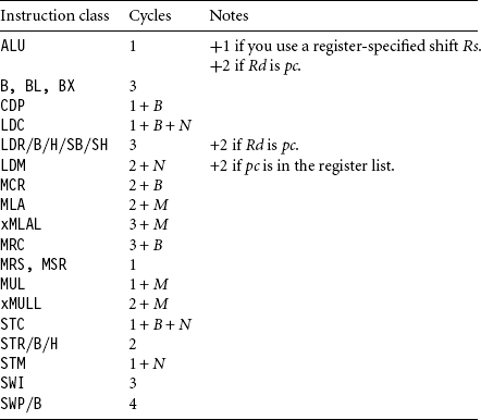
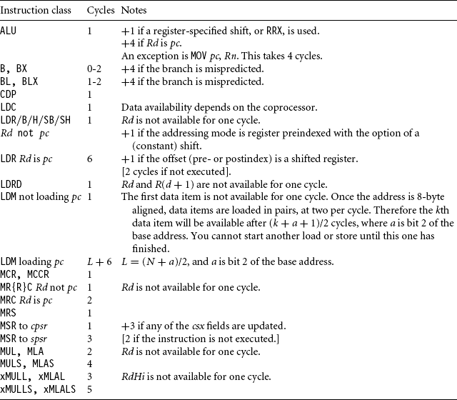
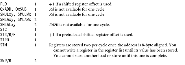
D.2 ARM7TDMI INSTRUCTION CYCLE TIMINGS
The ARM7TDMI core is based on a three-stage pipeline with a single execute stage. The number of cycles an instruction takes does not usually depend on preceding or following instructions. The multiplier circuit uses a 32-bit by 8-bit multiplier array with early termination. The number of multiply iteration cycles M depends on the value of register Rs according to Table D.3. Table D.4 gives the ARM7TDMI instruction cycle timings.
Table D.3
ARM7TDMI multiplier early termination.
| M | Rs range (use the first applicable range) | Rs bitmap s = sign bit x = wildcard-bit |
| 1 | −28 ≤ x < 28 | ssssssss ssssssss ssssssss xxxxxxxx |
| 2 | −216 ≤ x < 216 | ssssssss ssssssss xxxxxxxx xxxxxxxx |
| 3 | −224 ≤ x < 224 | ssssssss xxxxxxxx xxxxxxxx xxxxxxxx |
| 4 | remaining x | xxxxxxxx xxxxxxxx xxxxxxxx xxxxxxxx |
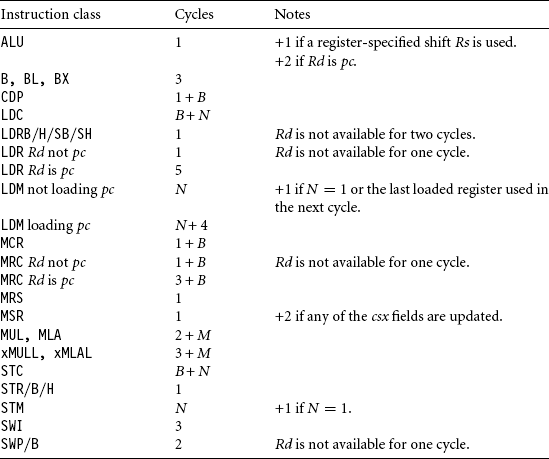
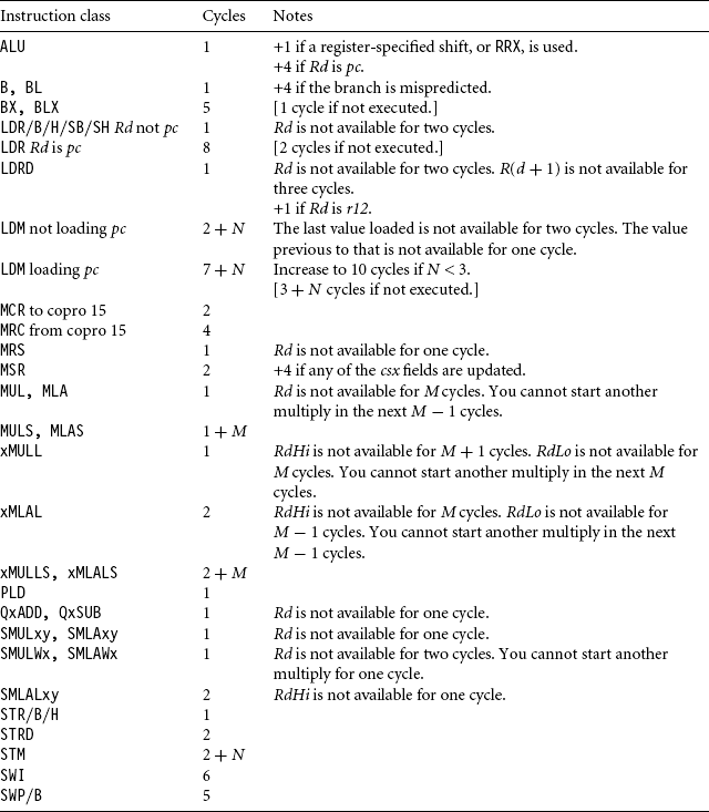
D.3 ARM9TDMI INSTRUCTION CYCLE TIMINGS
The ARM9TDMI core is based on a five-stage pipeline with a single execute stage and two memory fetch stages. There is usually a one- or two-cycle delay following a load instruction before you can use the data. Using data immediately after a load will add interlock cycles. The multiplier circuit uses a 32-bit by 8-bit multiplier array with early termination. The number of multiply iteration cycles M depends on the value of register Rs according to Table D.5. Table D.6 gives the ARM9TDMI instruction cycle timings.
Table D.5
ARM9TDMI multiplier early termination.
| M | Rs range (use the first applicable range) | Rs bitmap s = sign bit x = wildcard-bit |
| 1 | −28 ≤ x < 28 | ssssssss ssssssss ssssssss xxxxxxxx |
| 2 | −216 ≤ x < 216 | ssssssss ssssssss xxxxxxxx xxxxxxxx |
| 3 | −224 ≤ x < 224 | ssssssss xxxxxxxx xxxxxxxx xxxxxxxx |
| 4 | remaining x | xxxxxxxx xxxxxxxx xxxxxxxx xxxxxxxx |
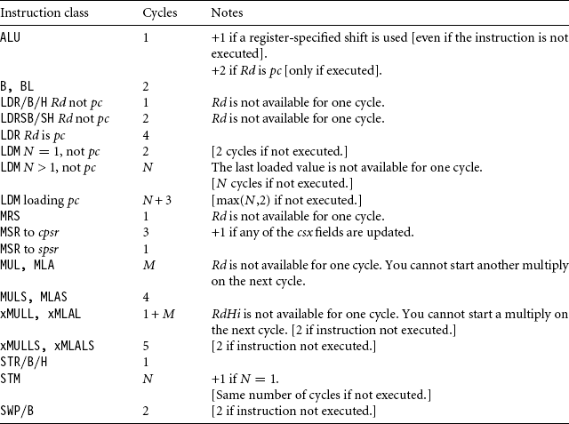
D.4 STRONGARM1 INSTRUCTION CYCLE TIMINGS
The StrongARM1 core is based on a five-stage pipeline. There is usually a one-cycle delay following a load or multiply instruction before you can use the data. Additionally, there is often a one-cycle delay if you start a new multiply instruction immediately following a previous multiply instruction. The multiplier circuit uses a 32-bit by 12-bit multiplier array with early termination. The number of multiply iteration cycles M depends on the value of register Rs according to Table D.7. Table D.8 gives the StrongARM1 instruction cycle timings.
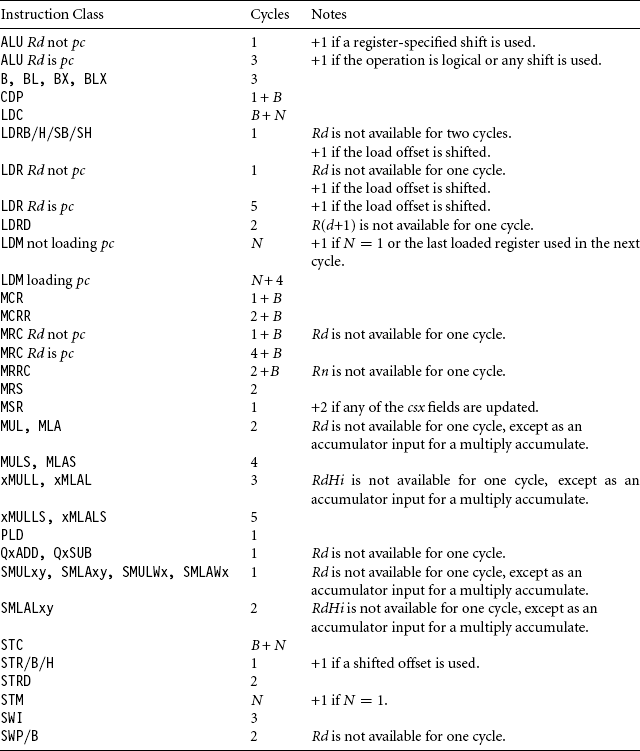
D.5 ARM9E INSTRUCTION CYCLE TIMINGS
The ARM9E core is based on a five-stage pipeline. There is usually a one- or two-cycle delay following a load or multiply instruction before you can use the data. The multiplier circuit uses a 32-bit by 16-bit multiplier array. The multiplier does not terminate early. Table D.9 gives the ARM9E instruction cycle timings.
D.6 ARM10E INSTRUCTION CYCLE TIMINGS
The ARM10E core is based on a five-stage pipeline with branch prediction. There is usually a one-cycle delay following a load or multiply instruction before you can use the data. The ARM10E uses a 64-bit-wide data bus, so load and store instructions can transfer 64 bits per cycle. The multiplier does not use early termination. Table D.10 gives the ARM10E instruction cycle timings.
D.7 INTEL XSCALE INSTRUCTION CYCLE TIMINGS
The Intel XScale is based on a seven-stage pipeline. There is usually a two-cycle delay following a load instruction before you can use the data. Multiply instructions usually issue in a fixed number of cycles, but then the result is not available for a variable number of cycles, depending on the value of Rs. Table D.11 shows how the number of multiply iteration cycles M depends on the value of Rs. Table D.12 gives the Intel XScale instruction cycle timings.
D.8 ARM11 CYCLE TIMINGS
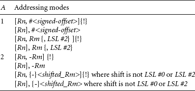
The ARM11 core uses an eight-stage pipeline with three execute stages. There is usually a two-cycle delay following a load instruction before you can use the data. Some operations such as shift, multiply, and address calculations require their input registers a cycle early.
For example, the following code sequence will stall the core for three cycles because the result of the load is not available for two cycles, and the input to the shift is required one cycle early:
![]()
The ARM11 core has a separate address generation unit that can calculate simple addresses in one cycle. More complicated addresses take two cycles. Table D.13 defines the number of address calculation cycles A for each addressing mode.
The ARM11 core uses prediction to minimize the number of cycles caused by a change in program flow. To enable prediction, set bit 11 of CP15 register c1. There are three branch predictors.
A static predictor predicts relative branches that are not recorded in the branch prediction cache. This is the case the first time the processor sees a given branch. The static predictor predicts forward conditional branches as taken and backward conditional branches as not taken.
A dynamic predictor predicts relative branches that are recorded in the branch prediction cache. The branch prediction cache has 128 entries based on the branch instruction address. Each cache entry predicts the branch destination and if the branch is taken. A cache entry has four states: strongly not taken, weakly not taken, weakly taken, strongly taken. Each time the branch is taken, the state moves one to the right in this list (if it can), and each time the branch is not taken, the state moves one to the left in this list (if it can).
A return stack predicts unconditional subroutine return instructions. The stack has three entries storing the return address from the three deepest BL, BLX subroutine calls.
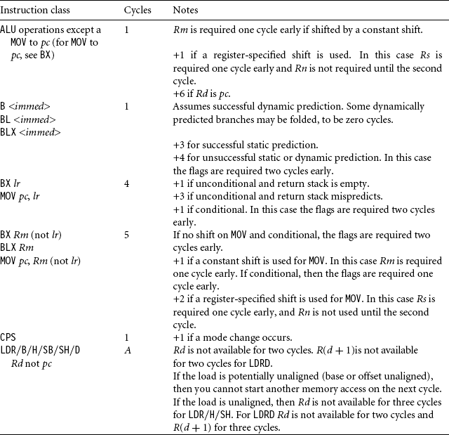
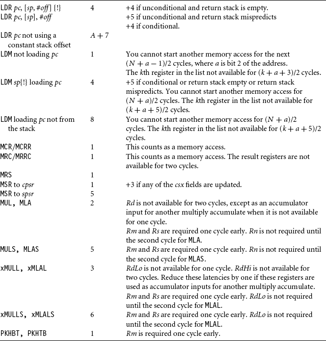
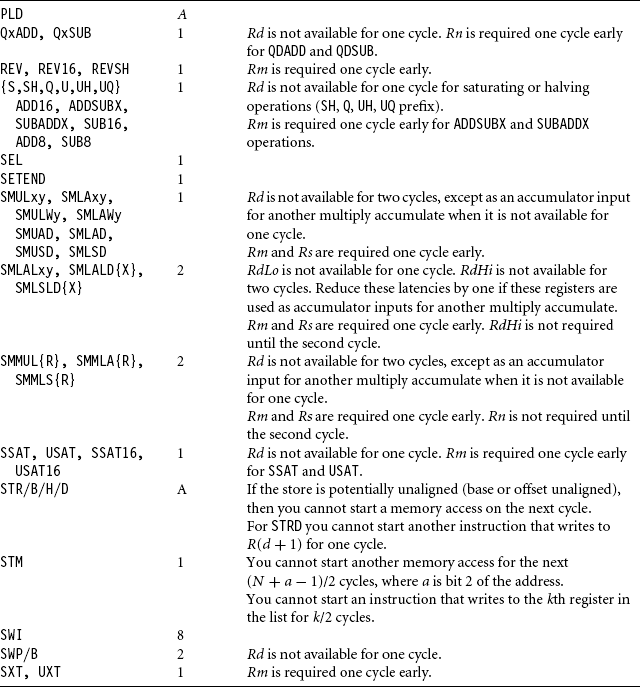
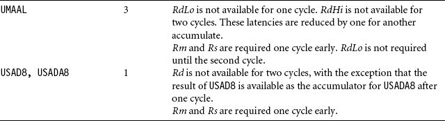
Table D.14 gives the ARM11 instruction cycle timings.