
CHAPTER 3
TINY POLARIZERS, SECRET OF THE NEW TECHNIQUE
3.1 INTRODUCTION
The idea of electromagnetic (EM) imaging for data encoding in chipless radiofrequency identification (RFID) systems was briefly introduced in Chapter 2. It was shown that imaging technique differs from other conventional methods as it provides extra spatial diversity. In imaging approach, each small section of the tag is separately scanned while it independently carries data. Providing fine scanning resolution governs the frequency band of operation and mandates the synthetic aperture radar (SAR) technique. However, the next issue that shall be answered is how to encode data in a small area of millimeter order.
Earth imaging system, the first and most important application of EM imaging, may suggest an approach for data encoding. In earth imaging, the earth's surface is interrogated by a radar system that is normally mounted on an air-/spacecraft. Based on the reflected signal, the radar system forms the related EM image of the earth. The strength of the reflected signal from each section of the earth's surface is linked to the image and shows the terrain of the earth. Rough surfaces result in higher reflection and therefore a brighter part in the EM image, for example, a building or mountain. An impinged signal on a flat surface is reflected in the opposite direction, by Snell's law; hence, radar receives no energy and a dark section in the image is formed. Figure 3.1 shows the principle of image brightness in an earth imaging system. This may initiate the idea of shaping the RFID tag surface in such a way to create a unique image when illuminated by a proper EM signal.
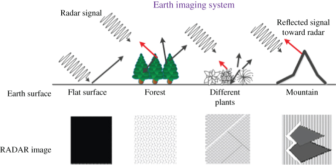
Figure 3.1 Reflection strength based on terrain roughness in earth imaging system [1].
Considering the tag cost expectation of less than one cent (1¢), the tag shall be shaped by only combining conductive and nonconductive sections. Moreover, elements on the tag structure shall be very simple; otherwise, system performance will be significantly degraded due to the noticeable printing errors on the millimeter-band 60 GHz. The simplest idea is a structure similar to a barcode as shown in Figure 3.2. Conductive and nonconductive strips may create different levels of reflection similar to earth imaging process; hence a unique EM image will be resulted.
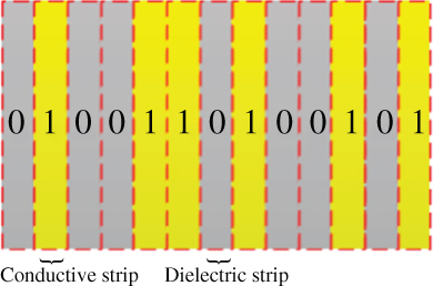
Figure 3.2 Initial proposed tag structure based on earth imaging concept.
To examine this idea, two separate conductive and dielectric strips are simulated through 3D full-wave CST software at the band 57–64 GHz. The strips are illuminated by a linearly polarized plane wave and the backscattered signals on the reader side are measured. The results are shown in Figure 3.3 with 30 cm reading distance. The incident electric field is 1 V/m, and it is parallel to the main axis of the strip. Interestingly, reflection from a conductive strip is higher than that of the dielectric strip, which contradicts with what was expected from the earth imaging system. Two reasons may be suggested. First, the illumination angle between the reader antenna and the tag is 90°. This means that all of the impinged energy to the conductive strip is reflected back toward the reader according to Snell's law. While for the dielectric surface, some of the incident energy is spread out due to its rougher surface. A squint angle other than 90° results in higher reflection toward the radar from a rougher surface as shown in Figure 3.1 for the earth imaging application. Second, the received signal in the earth imaging is only based on the reflected signal. While for the RFID tag imaging, the impinging signal induces a surface current on the conductive strip surface, which acts as a second source of electromagnetic emission.
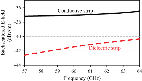
Figure 3.3 Backscattered signals from different types of strips; simulation result.
Irrespective of higher reflection from a conductive strip than a dielectric, the main issue is the very close signal level of the two strips type. The difference between two scenarios is less than 3 dBm. This is not a reliable field strength difference especially considering that it is a simulation result. It would be very difficult to separate reflections from conductive and dielectric strips in a real scenario, especially when the clutter and multipath effect of the surrounding objects are considered. Changing the polarization of the incident E-field does not affect the ratio of the received signal from conductive and dielectric strips.
While it appears that the signal-level approach similar to the earth imaging application is not able to provide a reliable way for tag imaging, the unique behavior of a conductive strip suggests an interesting approach to data encoding on the tag surface, which is discussed in the following section.
3.2 SWEETNESS OF DIFFRACTION
Finding a reliable approach for tag shaping, strips with varying widths, as shown in Figure 3.2, are interrogated at various illumination angles and polarization schemes. Although the signal levels have not changed enough to provide a reliable approach for the data encoding algorithm, a very interesting phenomenon was observed during the simulation. It was noticed that the backscattered signal from a narrow conductive strip shows elliptical polarization behavior while the strip is illuminated by a linearly polarized signal. This means that the conductive strip is capable of changing the polarization of the incident signal. It was found that for a narrow conductive strip, the backscattered signal may include a polarization component that is orthogonal to the polarization of the incident signal; hence the conductive strip acts as an EM polarizer. The depolarization aspect of the conductive strip suggests working on a cross-polar basis instead of a copolar basis. The theory behind this behavior of the conductive strip as an EM polarizer is discussed.
3.2.1 Diffraction, Kobayashi Potentials
Different phenomena are involved when a conductive strip is illuminated by an EM signal, reflection, refraction and diffraction, for example. As a strip has a finite surface with straight edges, it can behave differently based on the polarization and frequency of the incident wave as well as strip size and its orientation. Reflection based on Snell's law is the normal behavior that is expected for a wide strip, compared to the wavelength. However, when the strip is narrow enough, diffraction would be of more concern and act as the dominant phenomenon. In the past decades, many studies investigated diffraction from a metallic strip or a slot in a metal plane using various numerical and analytical techniques [2–9]. All research and studies on diffraction can be summarized as follows [10]:
- Geometric optics (GO) [3]
- Physical optics (PO) [4]
- Geometrical theory of diffraction (GTD) [5]
- Uniform asymptotic theory of diffraction (UAD) [6]
- Uniform theory of diffraction (UTD) [5]
- Physical theory of diffraction (PTD) [7]
- Spectral theory of diffraction (STD) [8]
- Method of equivalent current (MEC) [9]
- Hybrid methods.
Each method has its own advantages and limitations. Among them, geometrical optics (GO), PO, and uniform theory of diffraction (UTD) are the most common approaches. The Kobayashi potential (KP) method is an analyticonumerical technique used as an alternative to previously mentioned techniques with more accurate results and less procedure complexity [11]. Diffraction by a conductive strip on a dielectric slab has been thoroughly studied by Imran [12]. The far field pattern and induced surface current on an infinite strip etched to a dielectric slab based on the polarization of the incident plane wave is formulated in this work.
Figure 3.4 shows the geometry of the diffraction phenomenon where a conductive strip with negligible thickness etched on a dielectric slab is illuminated with a plane wave. The plane wave incident angle is Φ0. The strip width is 2a and it is infinite in the z direction. The diffracted wave depends on the polarization of the plane wave. Two separate polarizations are considered: (i) Parallel polarization, ![]() , and (ii) orthogonal polarization,
, and (ii) orthogonal polarization, ![]() .
.
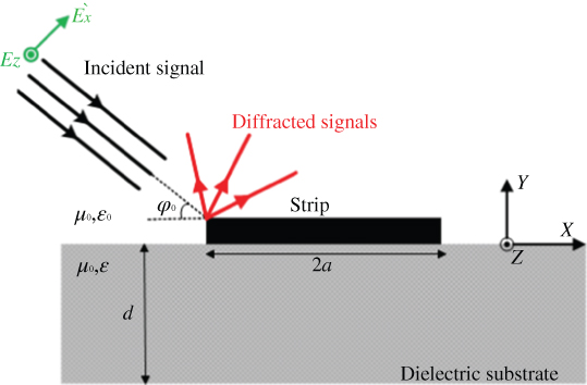
Figure 3.4 Geometry of diffraction by conductive strip on dielectric slab.
In the parallel polarization, the incident E-field is parallel to the main axis of the strip; the backscattered signal may have components in the x or z direction. The copolar and cross-polar components are defined by Equations (3.1) and (3.2), respectively [12]:
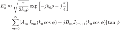
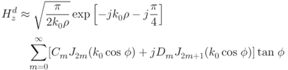
In the orthogonal polarization, in which the incident E-field is orthogonal to the polarization of the strip main axis, the copolar and cross-polar components are found from Equations (3.3) and (3.4), respectively:

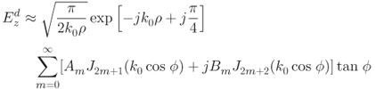
In the above expressions, Jm is the Bessel function, (ϕ,ρ) is the coordinate of the observation point, and ![]() is the normalized wave number. Am, Bm, Cm, and Dm are the expansion coefficients and should be found separately by numerical approaches and through the following expressions [12]:
is the normalized wave number. Am, Bm, Cm, and Dm are the expansion coefficients and should be found separately by numerical approaches and through the following expressions [12]:
where n = 0, 1, 2,…, M is the admittance parameter and
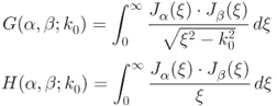
A comprehensive derivation of the above expressions based on the different values of the parameters has been provided in Ref. [12]. Among these results, the relation between the strip width and the cross-polar component is the concern. As shown in Ref. [12], the normalized wave number affects the level of the cross-polar component. Moreover, the cross-polar component is dependent on the angle of observation. For a certain value of the normalized wave number, that is relevant to the strip width, the maximum cross-polar component is achievable over a wide range of observation angles. The copolar and cross-polar components of the diffracted signal are figuratively shown in Figure 3.5. This figure shows that a well-designed strip is capable of creating significant cross-polar components while illuminated by a linear polarized incident signal.
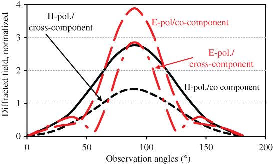
Figure 3.5 Copolar and cross-polar components of diffracted signals, linear scale.
This is an interesting result of diffraction. It simply means a strip with adequate dimensions may create noticeable cross-polar components in the backscattered signal. Hence, a simple strip line acts as an effective EM polarizer. This interesting aspect of the diffraction is used to suggest an effective data encoding algorithm in a chipless tag. One may recall that diffraction was the main issue in the barcode system as it limits the barcode's data encoding capacity and its reading range. In contrary, diffraction provides reliability and robustness in the proposed technique of imaging as will be shown.
3.3 STRIP-LINE POLARIZER
In the previous section, the cross-component of the backscattered signal from a narrow strip with infinite length due to the diffraction effect has been discussed. This simply means that the diffracted signal by the strip edge creates a cross-polar component. In addition to the diffraction effect, it is possible to maximize the cross-polar component of the backscattered signal by utilizing the resonance behavior of the strip-line structure. In a real scenario, the strip has a finite length; hence it is possible to design the length of the strip to resonate at a particular frequency. Maximizing the cross-component, one may suggest orienting the strip at 45° angle with respect to the incident plane wave. Therefore, the induced current on the strip surface, as a secondary source of EM wave, emits signal in both copolar and cross-polar directions as shown in Figure 3.6. It is important to note that in this scenario, the length of the strip plays a major role, while in diffraction phenomenon, the strip width is the main factor for cross-component creation.
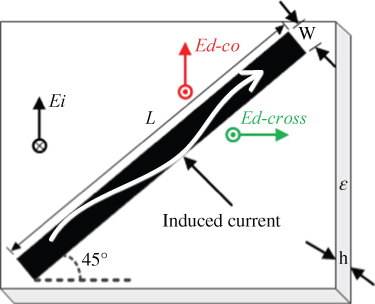
Figure 3.6 Strip orientation for creating cross-polar components, L = 1.45, w = 0.2, ϵ = 2.55, h = 0.0127, all in millimeters.
The strip line shown in Figure 3.6 is simulated as an EM polarizer through a full-wave EM solver CST microwave studio. A linearly polarized plane wave illuminates the strip, while the incident E-field maintains 45° angle with the strip axis. Two E-field probes are oriented at a certain distance, 30 cm, for example, to measure the copolar and cross-polar backscattered signal. The results of the simulation are shown in Figure 3.7. The cross-polar component of the backscattered E-field shows peak and the copolar component shows null at the resonant frequency. This is due to the fact that the antenna (resonant) mode RCS cancels the structural mode RCS at the copolar direction [13]. In contrary, in the cross-polar direction, only the resonant mode is dominant; hence, the cross-polar component shows a peak value. This cross-polar component is immune to the copolar structural mode. As is clear from the figure, in a certain band depending on the strip length, the cross-polar component is significant and hence the strip line can be considered as an effective EM polarizer.
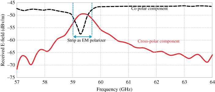
Figure 3.7 Simulated copolar /cross-polar components of backscattered signal, single strip line, L = 1.45, w = 0.2, ϵ = 2.55, h = 0.0127, all in millimeters.
3.4 MEANDER-LINE POLARIZER
A meander-line polarizer consists of at least one layer of meander-line-shaped conductors, usually printed on a circuit board [14]. A plane wave with 45° incident angle with respect to the principal axis of the meander line illuminates the structure as shown in Figure 3.8. The incident field can be decomposed into vertical and horizontal components. Each component experiences different phase shifts to provide 90° phase shift difference, while their amplitudes remain equal. As a result, the combined field in the transmitted signal is a circular polarized wave, and, therefore, the component is called transmission EM polarizer [14] (see Figure 3.8). Normally, multiple layers of meander lines are required to create a complete circularly polarized transmission signal [14–16]. A transmission meander-line polarizer also acts in the reverse direction and can convert a circular polarized (CP) wave into a linear-type signal. This type of meander-line structure is widely used in satellite communications [17, 18].
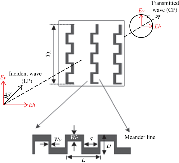
Figure 3.8 Meander line as transmission EM polarizer.
In the proposed application of the chipless RFID system, a reflection-type EM polarizer is required as the reader normally measures the backscattered signal by the tag. A possible solution for a reflection EM-polarizer structure is shown in Figure 3.9. The structure utilizes multilayer meander lines with a ground reflector. The linearly polarized incident wave (Ei) is converted into a circular polarization wave while passing the multilayer meander-line structure. For the x-polarized incident signal shown in Figure 3.9, the passing signal from the meander-line structure is a left-hand circular polarized (LHCP) wave, for example. This wave is completely reflected back by the ground plane while its rotation direction is reversed. Hence, the new wave with right-hand circular polarization (RHCP) is inserted in the multilayer meander-line structure again. This signal is converted into a linear polarized wave as the meander line changes the input circular polarized (CP) signal to a linearly polarized (LP) wave. However, the E-field of the final reflected wave (Er) is orthogonal to the direction of the E-field of the original incident wave (Ei). Hence, the goal of the meander line as a reflection EM polarizer is achieved.
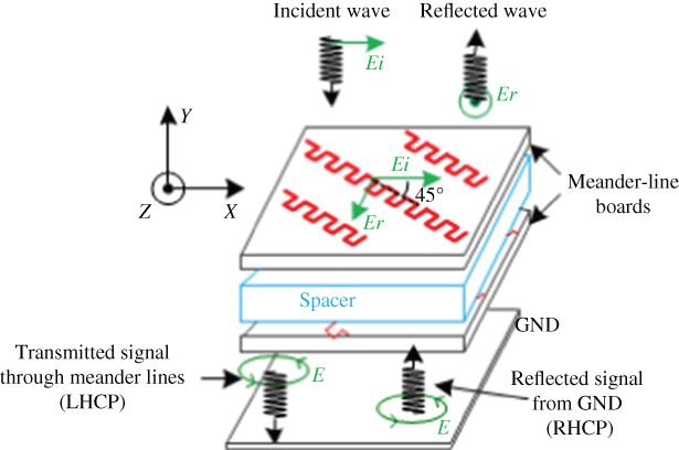
Figure 3.9 Multilayer meander-line structure for reflection EM polarizer.
While the proposed approach of the multilayer meander line with a ground plane reflector is technically appropriate for the purpose of reflection-type EM polarizer, it would not be a suitable solution for chipless RFID tag structure. The multilayer tag structure contradicts with the expected subcent tag cost that is only addressed through a single-layer printable tag structure. Therefore, to propose a single-layer polarizer, the meander-line dimensions have been redesigned based on diffraction and resonance principles similar to those for the strip-line polarizer. This means that the parameters of the meander-line structure as shown in Figure 3.8 are designed to maximize the cross-polar component of the backscattered signal. Similar to the case of the strip line, again both diffraction and resonance behaviors of the meander line are used simultaneously for the maximum cross-polar component. The expectation is to achieve better performance from the meander line due to the increased design freedom. While the strip line has mainly two design parameters, strip width and length, the meander-line structure has more design parameters: Wh, Wv, D, S, and L.
A single-layer meander line is designed through parameter optimization in CST aiming to provide the highest cross-polar backscattered signal. The structure is assumed to have the same length as that for the strip line. The simulation result is shown in Figure 3.10, while the parameters of the design for the strip line and meander line are as follows:
- For the strip line: TL = 1.6, α = 0.2
- For the meander line: TL = 1.6, Wh = 0.2, Wv = 0.1, D = 0.37, L = 0.5 (all values in millimeters), and ϵr = 2.55
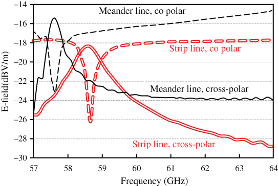
Figure 3.10 Simulated copolar/cross-polar component of single-layer strip line and meander-line structure.
It is clear from Figure 3.10 that the meander line's cross-polar component acquires sharper resonance for the same polarizer length (TL = 1.6 mm). Moreover, the cross-polar E-field component of the meander line is 2–3 dB higher than that of the strip line. This equals to 5 dB more received power level. The higher cross-polar component sets freedom on the reading distance and better signal-to-noise ratio (SNR) of the system.
3.5 MULTIPLE POLARIZERS
The range and azimuth resolutions were introduced in Chapter 2. It was also shown that the fine range resolution of millimeter order is not possible to achieve due to the limited available frequency band. Therefore, the azimuth resolution is the only factor that can be used for providing the required spatial diversity for data encoding purpose in a chipless RFID system. This means that the detectable pixels on the tag surface are rectangle with few millimeters width and length of tens of centimeters order, as shown in Figure 3.10. Each rectangle independently encodes a certain amount of data. Considering the shape and dimensions of the suggested EM polarizer as encoding elements, it is expected that each rectangle may include multiple polarizers for increasing the encoding capacity if polarizers with different lengths and hence different resonance frequencies are used. Alternatively, one may use similar polarizers on each rectangle for higher RCS, which results in better SNR or a longer reading range. Hence, the final shape of the chipless tag for encoding purpose is shown in Figure 3.11. As multiple polarizers are suggested on each rectangle, it is important to investigate the effect of coupling among the polarizers. Process tolerance is also expected during tag fabrication; hence, it is very beneficial to explore the fabrication error on the final performance of the system. Doing these works, each scenario is first simulated and then compared with the measurement result.
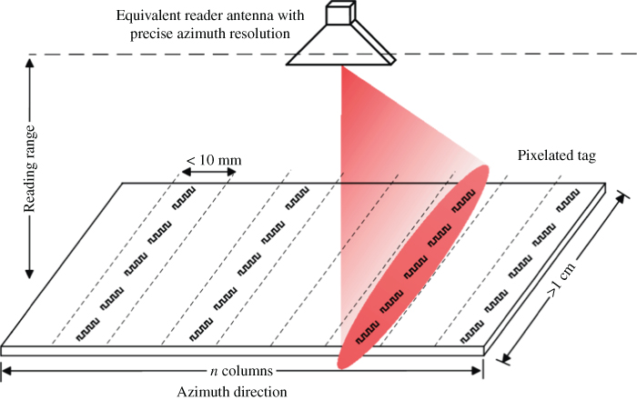
Figure 3.11 Final tag structure for data encoding purpose.
3.5.1 Multiple Similar Strips, Coupling Effect
To find out the effect of coupling among polarizers on each rectangle, it is easier to start with multiple strips with the same dimensions. It is also beneficial to explore the effect of multiple similar polarizers on increasing the signal level for longer reading ranges or satisfying SNR.
If an accurate and precise fabrication process is utilized for tag manufacturing, then it is reasonable to expect that all the strip lines have exactly the same dimensions. Obviously, if the strip lines are of the same length and width, then a similar response to what is shown in Figure 3.7, with a higher received E-field level, is expected. To validate this expectation, five strip lines with the same dimension are placed near to each other (1 mm distance). The simulated copolar and cross-polar backscattered E-fields are shown in Figure 3.12. Comparing Figures 3.7 and 3.12, one notices the following phenomena:
- i. Resonance frequency shifts from 59.5 to 58.2 GHz, about 1.3 GHz.
- ii. Resonance bandwidth spread from 0.7 to 1 GHz.
- iii. Amplitude of the backscattered signal increases by approximately 6.5 dB from −49 to −42.5 dB/m. This is approximately five times (10 × log 5 = 7 dB) amplification as expected.
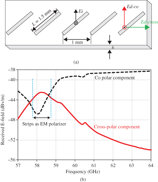
Figure 3.12 (a) Five strip lines with same length and (b) simulated copolar/cross-polar backscattered signals.
Both (i) and (ii) can be related to the coupling among strips as they were placed very close to each other (1 mm). This means that Figure 3.12 is not simply a multiplication of Figure 3.7. However, the initial expectation on the received power level has been almost confirmed.
3.5.2 Multiple Different Strips, Smeared Resonance
The effect of multiple strips with the same dimension has been considered in the previous section. It is useful to explore the system capability on providing higher data encoding capacity on each rectangle of the tag by combining multiple polarizers with different dimensions and hence various resonance frequencies. This means that the suggested approach of spatial diversity is combined with conventional frequency-signature technique for higher content capacity. Therefore, multiple polarizers, strip lines, with slightly different lengths are simulated.
Multiple strips with slightly different lengths are placed close (1 mm) to each other. Five strip lines, whose lengths vary from 1.6 to 1.7 mm, are considered. Figure 3.13 shows the simulation results. For ease of comparison, the result of a single strip is also reproduced in this figure. It is clear from Figure 3.13 that the response from multiple strips with different lengths does not show any resonance behavior. There are some fluctuations on the received signal level, but detection of the resonances is very difficult if not impossible. The mutual coupling as discussed is one of the factors. Moreover, one may suggest that each strip line is resonating at different frequency and hence the result is the combination of all resonances and hence no specific resonance is detectable. The importance of this result is revealed when a printed tag structure is considered.
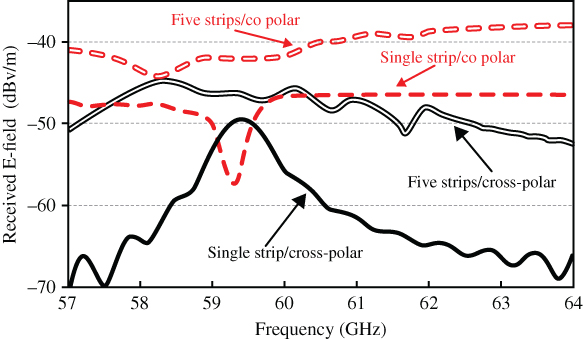
Figure 3.13 Simulated copolar/cross-polar components of backscattered signal.
3.6 POLARIZER FABRICATION
Proposed structures of strip line and meander lines as EM polarizers are fabricated for measurement purpose. First, polarizer-based tag is fabricated through an accurate photolithographic process on a dielectric structure. Then, the same tag structure is printed with a SATO inkjet printer that utilizes conductive ink on a paper substrate. These two tag samples through different fabrication processes are carefully investigated by an electronic microscope regarding their precise dimensions and shapes. It will be shown that the printed sample suffers severely from shape anomalies and changes in dimensions due to the printing resolution of the commercial printing technology.
3.6.1 Photolithographic Fabrication Process
The suggested polarizers in the previous section are designed and simulated based on the Taconic TLX-8 substrate with ϵr = 2.55 and 0.127 mm thickness. The conductive part is the annealed copper with 1 oz thickness. The design accuracy is 0.05 mm. It is possible to fabricate a single polarizer; however, as shown before, more than one polarizer are placed in each rectangle of the tag surface. The designed polarizers, strip line, and meander line are fabricated through a photolithographic process. The photographs of these two polarizers are shown in Figure 3.14.
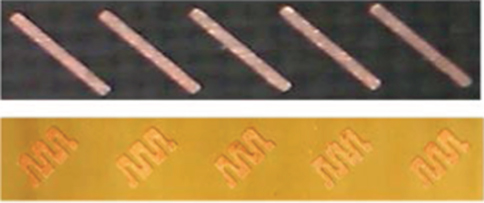
Figure 3.14 Fabricated EM polarizers through photolithographic process.
3.6.2 Printed Polarizer
It was thoroughly discussed in the previous chapters that any suggestion for chipless RFID systems shall be based on the printed tag structure. Otherwise, obtained results based on perfect materials and costly fabrication processes do not guarantee the successful performance of any proposed approach at the commercial stage. This is the most significant phase of the work in each proposed technique for chipless RFID systems. To evaluate the performance of the proposed approach, the polarizers are printed by a SATO GL4e industrial thermal silver ink-based printer with a 600 dpi resolution [19]. SATO uses aluminum-based ink as the conductor and normal paper as the substrate. Figure 3.15 shows the SATO printer and the printed polarizers. The final printed structures are measured with an electronic microscope and the values are shown in the figure. The actual lengths of printed strip lines are normalized to show the difference among final printed structures and the designed lengths. For the meander-line case, the final dimensions are not shown due to the large number of design parameters for each object. Instead, the micrograph of a printed meander line is highlighted that clearly shows the anomalies occurring during the printing process.
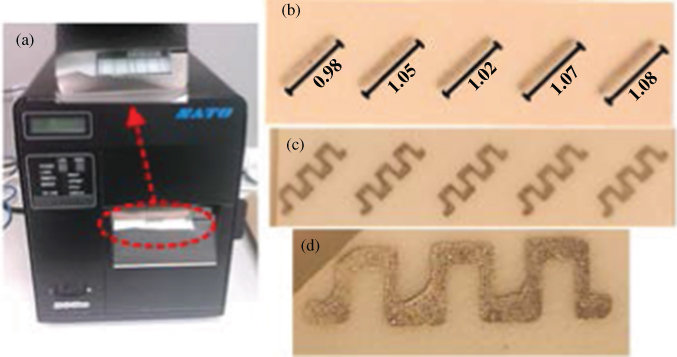
Figure 3.15 (a) SATO printer, (b) printed strip lines, (c), and (d) printed meander lines.
The effect of process errors on the polarizer's performance is shown in the following chapter when tags are measured in a real environment. However, it is possible to predict the effect of printing errors on the backscattered signal. Each printed strip line has a certain length and hence resonance at different frequency than what expected by simulation and design. This means that in real scenarios, it is not possible to have multiple printed strip lines with the same dimensions. Therefore, creation of multiple similar strip lines as discussed in Section 2.6 is not practically possible due to the limitation in printing accuracy of the commercial printing technologies. Instead, the situation discussed in Section 3.5.2, multiple different strip lines, is happening and so no specific resonances can be expected from a group of strip lines with slightly different dimensions. In conclusion, the combination of the frequency-signature technique with spatial diversity is actually not practical and the data encoding shall rely solely on the spatial diversity. This claim is confirmed by measurement in the following chapter.
3.7 CONCLUSIONS
Shaping of the tag surface for providing a unique image is discussed in this chapter. The similarities and differences between the earth imaging and tag imaging have been shown. It was found that due to the diffraction of EM wave from the edge of a strip line with proper dimensions, it is possible to expect the cross-polar component at the backscattered signal. This idea has been considered through KP approach. Then the effect of resonance response from an inclined strip line is added to the diffraction phenomenon to build the basis for the EM-polarizer base system. Meander line as a more effective EM polarizer has been introduced. The simulation results for a single polarizer and multiple polarizers were presented. The effect of multiple polarizers with slightly different dimensions on the cross-polar backscattered signal was then considered. It was found that a printed polarizer has inaccurate dimensions hence act similar to the multiple polarizers with different dimensions. This part is very important on proposing the correct approach for data encoding scenario in the proposed spatial-based system.
REFERENCES
- 1. JPL. (2013). Available: http://southport.jpl.nasa.gov/.
- 2. M.H. Williams, “Diffraction by a Finite Strip,” Oxford Journals, Mathematics & Physical Sciences, vol. 35, 1980.
- 3. M.C. Heaton, P.J. Joseph, and R.L. Haupt, “Uniform Theory of Diffraction Analysis for Conductive Strips with Constant and Tapered Resistive Loads,” in Antennas and Propagation Society International Symposium, 1991, p. 4.
- 4. U.Y. Ziya, “Physical Optics Theory for the Scattering of Waves by an Impedance Strip,” Optics Communications, vol. 284, p. 1760, 2010.
- 5. R.G. Kouyoumjian and P.H. Pathak, “A Uniform Geometrical Theory of Diffraction for an Edge in a Perfectly Conducting Surface,” Proceeding of the IEEE, vol. 62, 1974.
- 6. S.W. Lee, “Comparison of Uniform Asymptotic Theory and Ufimtsev's Theory of Electromagnetic Edge Diffraction,” IEEE Transactions on Antennas and Propagation, vol. 25, 1977.
- 7. T. Griesser and C.A. Balanis, “Backscatter Analysis of Dihedral Corner Reflectors Using Physical Optics and the Physical Theory of Diffraction,” IEEE Transactions on Antennas and Propagation, vol. 35, 1987.
- 8. R. Mittra, Y. Rahmat-Samii, and W.L. Ko, “Spectral Theory of Diffraction,” Applied Physics, vol. 10, 1976.
- 9. V.C. Monk and F.W. Sedenquist, “High-Frequency Radar Modeling,” Advanced Sensors Directorate Research, Development, and Engineering Center, Alabama, 1995.
- 10. J.B. Keller, “One Hundred Years of Diffraction Theory,” IEEE Transactions on Antennas and Propagation, vol. AP-33, p. 4, 1985.
- 11. A. Imran and Q.A. Naqvi, “Diffraction of Electromagnetic Plane Wave from a Slit in a PEMC Plane,” Progress In Electromagnetics Research vol. 8, 2009.
- 12. M.A. Imran, “Diffraction of Electromagnetic Plane Waves from Strips and Slits Using the Method of Kobayashi Potential,” PhD Thesis, Quaid-I-Azam University, Islamabad, 2010.
- 13. I. Balbin and N.C. Karmakar, “Phase-Encoded Chipless RFID Transponder for Large-Scale Low-Cost Applications,” IEEE Microwave and Wireless Components Letters, vol. 19, pp. 509–511, 2009.
- 14. A.K. Bhattacharyya and T.J. Chwalek, “Analysis of Multilayered Meander Line Polarizer,” International Journal of Microwave and Millimeter-Wave Computer-Aided Engineering, vol. 7, pp. 442–454, 1997.
- 15. L. Young, L.A. Robinson, and C.A. Hacking, “Meander-Line Polarizer,” IEEE Transactions on Antennas and Propagation, 21, 1973.
- 16. R.S. Chu and K. Lee, “Analytical Model of a Multilayered Meander-Line Polarizer Plate with Normal and Oblique Plane-Wave Incidence,” IEEE Transactions on Antennas and Propagation, vol. 35, p. 652, 1987.
- 17. M. Mazur and W. Zieniutycz, “Multi-layer Meanderline Polarizer for Ku-band,” in Microwave, Radar and Wireless Communications (MIKON-2000), p. 78.
- 18. F. Jian, “The Optimum Designing Method for Wide Bandwidth Meander-Line Circular Polarizer,” in Antennas, Propagation and EM Theory, ISAPE 2000, pp. 10–13.
- 19. SATO Australia (September 2014). Available: http://www.satoaustralia.com/.