
CHAPTER 9
CHIPLESS RFID TAG DESIGN
9.1 INTRODUCTION
In this chapter, the physical layer developments of the two chipless radiofrequency identification (RFID) tag types, experimental setup, and results are presented in microwave and millimeter-wave domains. The first tag type is a single input single output (SISO) tag having circular resonators that operates between 21 and 27 GHz. The second type is the novel multiple input multiple output (MIMO) tag having multiresonators that operates at the frequency band 2.4 GHz. A brief summary of the two tag types are given in Figure 9.1. The rest of the chapter describes the design of the tags and experimental verification of the proposed tag detection techniques in Chapter 10 and 11.
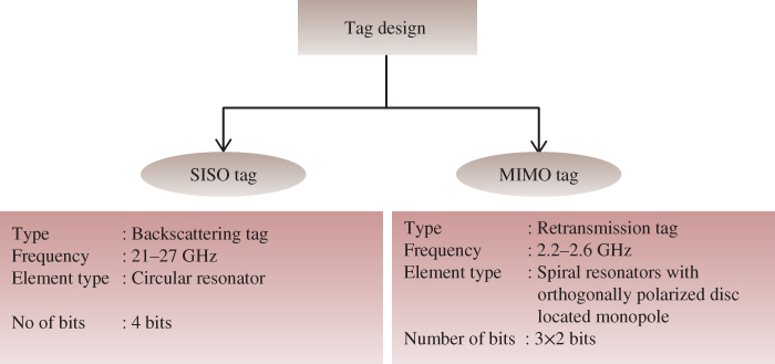
Figure 9.1 Tag types used in SISO and MIMO detection algorithm developments.
9.2 SISO TAG DESIGN
In this section, a circular patch resonator-based backscattering chipless RFID tag design is discussed. The tags are operating between 21 and 27 GHz frequency range. The tags are fabricated on a thin film paper using the SATO printer having a conductive ink. Then, the tags are read using an existing chipless RFID reader developed by Kalansuriya at Monash Microwave, Antenna, RFID and Sensor Laboratory, Monash University.
9.2.1 Tag Design and Fabrication
Figure 9.2 shows the photograph of a 4-bit tag designed at the 21–27 GHz ultrawide band (UWB).The tag is comprised of four sets of distinct resonators thoughtfully located so that nearby resonances are not interfered. The tag is designed to occupy 4 bits in the 21–27 frequency band. The resonance frequencies are selected as 22.5, 23.5, 24.5, and 25.5 GHz as simulation shows that the 3-dB bandwidth of each resonator response at this frequency band is about 1 GHz. The diameter of the circle is inversely proportional to the resonance frequency. The diameters for the above resonance frequencies are found and displayed in Table 9.1.
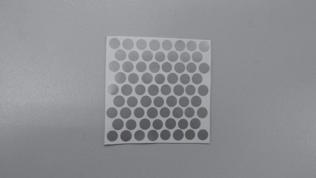
Figure 9.2 Printed tag.
Table 9.1 Simulation Parameters
| Resonance Frequency (GHz) | Diameter of the Circular Patch (mm) |
| 22.5 | 4.38 |
| 23.5 | 4.59 |
| 24.5 | 4.84 |
| 25.5 | 5.13 |
The specific frequency resonators are repeated to increase the backscattered signals of the individual resonators [1]. The tag is printed in-home using MMARS Laboratory's SATO printer. This monochrome printer has a resolution of 600 dpi. The substrate is 0.09-mm-thick glossy paper with a bulk silver coating of 10 μm on top. The design is thermally transferred to the paper substrate and the fully printable silver tag is created on the paper substrate.
9.2.2 Experimental Setup
In this section, the experimental setup used to verify the performance of the tags was designed. A chipless RFID reader that reads the magnitude of the tag response was used to read the tag designed in the previous section. An experiment was set up as shown in Figure 9.3. The reader transmits a narrow banded sinusoid signal using a transmit horn antenna and as shown in the figure the receiver receives the tag response for that frequency using a receive horn antenna. The magnitude of the received signal is recorded along with the frequency of the signal sent. Similarly, the frequency is swept across the 21–27 GHz band and the complete tag response is recorded.
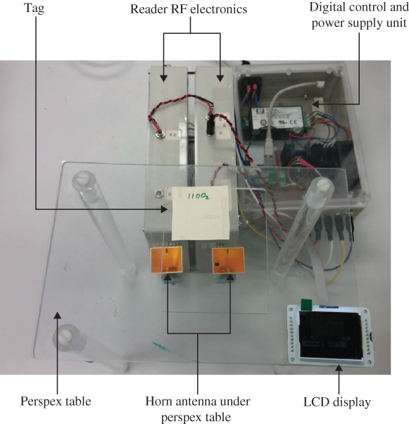
Figure 9.3 Experimental setup.
Figure 9.4 shows the tag response ([1111]) recorded by the chipless RFID reader. It can be seen that the four resonances occur at the designed resonating frequencies. The presence (ON) and absence (OFF) of the resonators can be selected to form 16 different tag types for a 4-bit tag as shown in Table 9.2 The circular patches having the same diameter increase the effective radar cross section and hence form a bigger frequency dip at the resonance frequency. The four resonator sets are selected such that tags with all 16 combinations can be designed. These 16 tag types are fabricated and used for testing the detection techniques derived in Chapter 10.
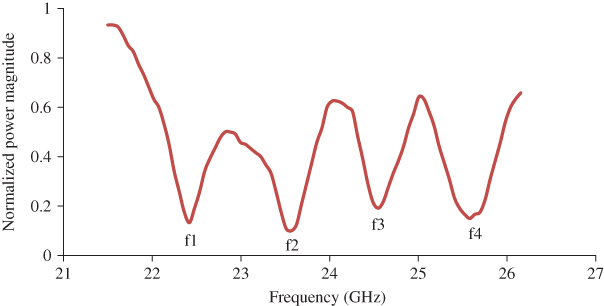
Figure 9.4 Magnitude of the tag response for tag [1111].
Table 9.2 Tag Types Given by Resonator Combinations
| Resonator Combinations | ||||
| Tag Type | f1 | f2 | f3 | f4 |
| [0000] | OFF | OFF | OFF | OFF |
| [0001] | OFF | OFF | OFF | ON |
| [0010] | OFF | OFF | ON | OFF |
| [0011] | OFF | OFF | ON | ON |
| [0100] | OFF | ON | OFF | OFF |
| [0101] | OFF | ON | OFF | ON |
| [0110] | OFF | ON | ON | OFF |
| [0111] | OFF | ON | ON | ON |
| [1000] | ON | OFF | OFF | OFF |
| [1001] | ON | OFF | OFF | ON |
| [1010] | ON | OFF | ON | OFF |
| [1011] | ON | OFF | ON | ON |
| [1100] | ON | ON | OFF | OFF |
| [1101] | ON | ON | OFF | ON |
| [1110] | ON | ON | ON | OFF |
| [1111] | ON | ON | ON | ON |
9.3 MIMO TAG DESIGN
One of the original contributions of the proposed MIMO-based chipless RFID system is the MIMO tag design. The main parts of the proposed chipless MIMO tag are identified as the power divider, monopole tag antennas, and multispiral resonators. These individual components are designed in computer simulation tool (CST) and their performance is verified. Following are the detailed descriptions of the component-level design and their integration to a complete MIMO tag.
9.3.1 Power Divider Design
The power divider needs to divide the power equally into two branches over a broadband of 400 MHz centered at 2.4 GHz. Therefore, a symmetrical T-junction power divider is designed. The design parameters are the length and the width of each transmission line presented in the divider. The designed and fabricated T-junction power divider is shown in Figure 9.5. The power divider is designed on TLX8 substrate with a relative permittivity (![]() ) of 2.4, loss tangent (
) of 2.4, loss tangent (![]() ) of 0.004, and thickness (
) of 0.004, and thickness (![]() ) of 0.5 mm. Both the simulated and the experimental S parameter magnitudes versus frequency for the power divider are shown in Figure 9.6. It is clear that both simulated and measured S21 and S31 are similar and close to the required value of
) of 0.5 mm. Both the simulated and the experimental S parameter magnitudes versus frequency for the power divider are shown in Figure 9.6. It is clear that both simulated and measured S21 and S31 are similar and close to the required value of ![]() (half power division). The measured and simulated S11 in decibels (return loss) versus frequency is also shown in the figure. There is a difference in the two curves and this is possibly due to fabrication defects, where it shifts the operating frequency little higher. As far as the performance is concerned, the fabricated power divider still has a bandwidth of over 500 MHz at
(half power division). The measured and simulated S11 in decibels (return loss) versus frequency is also shown in the figure. There is a difference in the two curves and this is possibly due to fabrication defects, where it shifts the operating frequency little higher. As far as the performance is concerned, the fabricated power divider still has a bandwidth of over 500 MHz at ![]() centered around 2.4 GHz. So the power divider performance is acceptable and any further tuning is not attempted. Once the satisfactory performance of the T-junction power divider is obtained, the next component designed is the monopole antenna.
centered around 2.4 GHz. So the power divider performance is acceptable and any further tuning is not attempted. Once the satisfactory performance of the T-junction power divider is obtained, the next component designed is the monopole antenna.
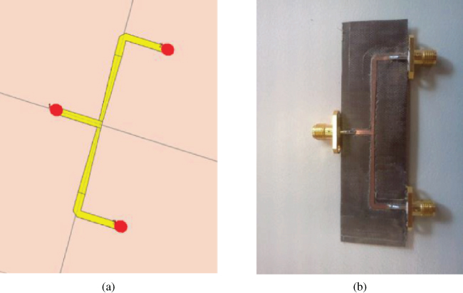
Figure 9.5 T-junction power divider. (a) CST design; (b) fabricated power divider. TLX8 substrate with  ,
,  and
and  mm.
mm.
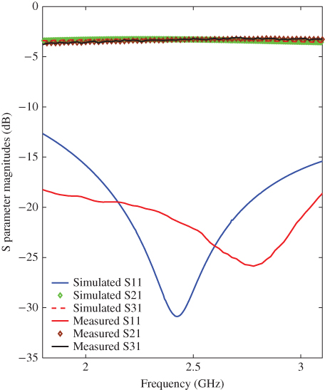
Figure 9.6 S-parameters of the power divider.
9.3.2 Monopole Antenna Design
A monopole antenna is designed to operate at 2.4 GHz with a bandwidth of 400 MHz. The monopole antenna is selected due to its figure-of-eight bream radiation pattern and distinct polarization so that vertical and horizontal antennas can be used to reduce the cross talk between the transmit and receive chains of the MIMO chipless RFID tag. A microstrip-based antenna with a circular patch is used for size optimization [2]. Figure 9.7 shows the monopole antenna design in CST as well as the fabricated antenna. The design parameters are the radius of the circular patch, gap between the ground plane, and disc edge and the dimension of the feedline [3].
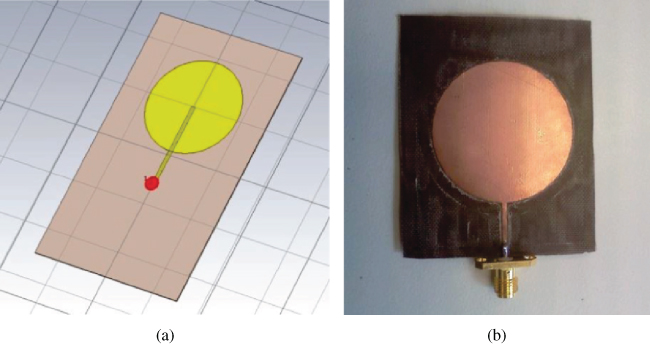
Figure 9.7 Monopole antenna. (a) CST design; (b) fabricated monopole).
The performance of the monopole antennas is presented next. Figure 9.8 shows the return loss versus frequency of the antenna obtained from both simulated and measured data. It can be seen that they both agree and the antenna has an operating bandwidth of over 400 MHz at ![]() .
.
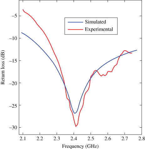
Figure 9.8 Return loss of the monopole antenna.
Figure 9.9 shows the antenna radiation pattern at 2.4 GHz, which is a figure-of-eight omnidirectional radiation pattern with the maximum gain of the main lobe with 2.7 dB, which is acceptable.
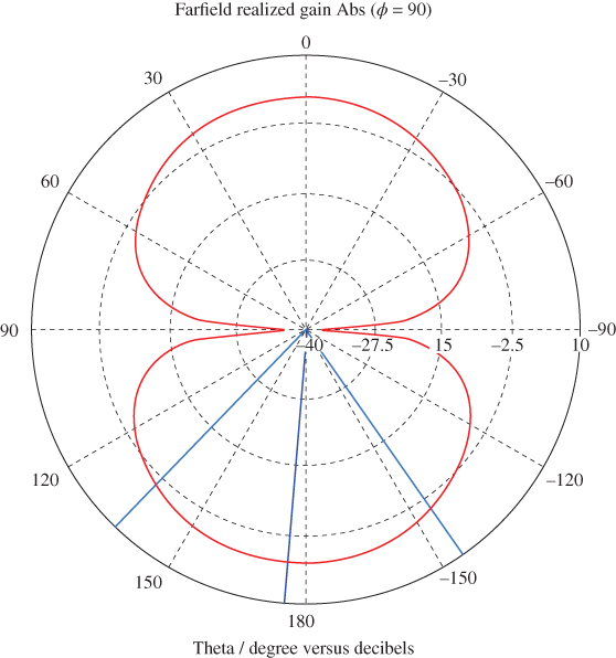
Figure 9.9 Simulated radiation pattern of the monopole antenna.
The realized gain of the antenna on the main lobe was analyzed over a bandwidth of 400 MHz centered around 2.4 GHz and the results are shown in Figure 9.10. It is clear that the realized gain is above 2.5 dB over the frequency band. These results verify the successful operation of the monopole antenna at a bandwidth of 400 MHz centered around 2.4 GHz. After obtaining satisfactory performance from the designed antenna, the spiral resonators are designed.
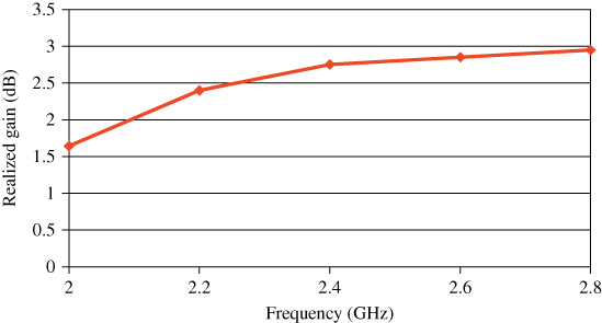
Figure 9.10 Realized gain of the monopole antenna.
9.3.3 Spiral Resonator Design
A set of spiral resonators are designed to operate at the resonance frequencies given by Table 9.1. Design parameters are the transmission line lengths, widths, and the gap between the microstrip lines [3]. Figure 9.11 shows both the CST designs on spiral resonators and one of the fabricated resonators.
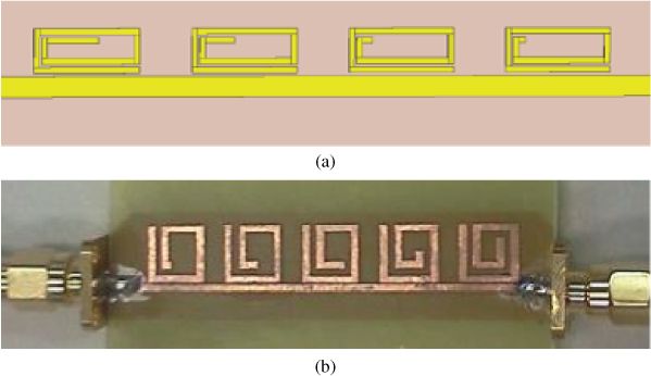
Figure 9.11 Spiral resonators. (a) CST design; (b) fabrication.
A spiral resonator response obtained from CST simulations is shown in Figure 9.12. It is clearly seen that both the amplitude and the phase contain the data and existing techniques mostly rely on only one of them. However, the proposed detection techniques use the information available in both amplitude and phase. A photograph of the fabricated MIMO tag with all “0” bits (no multiresonator) in branch connected to ![]() and all “1” bits in the branch connected to
and all “1” bits in the branch connected to ![]() is shown in Figure 9.13.
is shown in Figure 9.13.
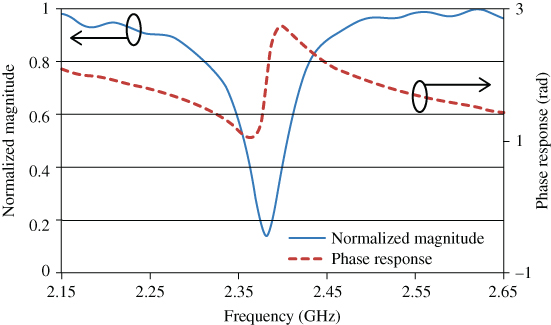
Figure 9.12 CST-generated resonator response.
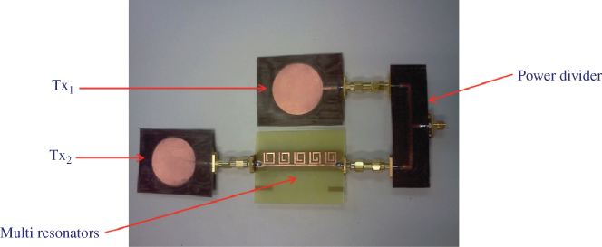
Figure 9.13 Fabricated MIMO tag.
9.3.4 Experimental Setup
The schematic of the experiment conducted to measure the MIMO tag response using an arbitrary waveform generator (AWG) and an oscilloscope with a high sampling rate is shown in Figure 9.14. However, antennas are replaced using cables as the sole purpose of this work is to verify the validity of the ML-based detection method.
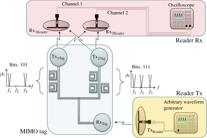
Figure 9.14 MIMO tag experiment.
Figure 9.15 shows the CST-generated tag response and the measured tag response for tag bits [1010]. ![]() measurements across the resonator are recorded using a performance network analyzer and converted from log scale to linear scale for comparison with the CST-generated response. It can be seen that they are closely matched.
measurements across the resonator are recorded using a performance network analyzer and converted from log scale to linear scale for comparison with the CST-generated response. It can be seen that they are closely matched.
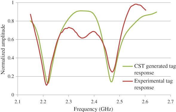
Figure 9.15 Tag response for [1010].
So far the design of a MIMO-based chipless RFID tag is discussed. Its individual component performances are analyzed using the CST-simulated results and experimental results. It is clear from Figure 9.15 that there are some anomalies between the theoretical and experimental results. This may be because of the coupling between the two branches in the MIMO tag. However, the proposed MIMO-based chipless RFID system has an inbuilt mechanism to overcome this challenge. Any coupling between the antennas can be incorporated into the ![]() MIMO channel matrix. This can be performed using a calibration tag. Now the system is free from any coupling between the two branches, and with the known channel, it is possible to perform tag detection.
MIMO channel matrix. This can be performed using a calibration tag. Now the system is free from any coupling between the two branches, and with the known channel, it is possible to perform tag detection.
9.4 CONCLUSIONS
After analyzing the simulations, it is noteworthy to pinpoint that, even though there are only two transmitting branches presented in the RFID tag considered, it is theoretically possible to add more branches and still recover the transmitted signals given that the number of receiving antennas in the reader is larger than or equal to the number of transmitting branches in the tag. Hence, without increasing the bandwidth, the bit capacity can be further increased using the same frequency resonators compared with having only one branch at the tag. However, it is required to evaluate the effect of mutual coupling between the antennas with higher number of transmitting branches in the tag.
In the RFID tag proposed, there is only one receiving antenna through which the received signal will be divided into two equal components. The proposed concept can be extended to having a dedicated receiving antenna for each component, hence increasing the effective signal-to-noise ratio (SNR) at each branch. Therefore, with multiple dedicated transmitting and receiving antennas on the tag performance can be improved further. In addition, the concept can be further extended to multiple tag detection if each branch is considered as a separate tag.
Furthermore, the use of IQ modulation/demodulation allows an extra degree of freedom to increase the bit capacity. Since the baseband signal considered is complex, it is possible to have asymmetric frequency response in positive and negative frequencies. Therefore, the eligible frequency band in the passband centered around the radiofrequency (RF) carrier doubles, allowing more resonators to be placed in the tag, without increasing the sampling rate of the ADC at the receiving end of the reader. After analyzing the above results, it can be concluded that MIMO is a competitive candidate for improving reliability or the bit capacity of a resonator-based chipless RFID system.
REFERENCES
- 1. P. Kalansuriya, N. Karmakar, and E. Viterbo, “On the detection of frequency-spectra-based chipless RFID using UWB impulsed interrogation,” IEEE Transactions on Microwave Theory and Techniques, vol. 60, no. 12, pp. 4187–4197, 2012.
- 2. S. Preradovic, I. Balbin, N. Karmakar, and G. Swiegers, “Multiresonator-based chipless RFID system for low-cost item tracking,” IEEE Transactions on Microwave Theory and Techniques, vol. 57, no. 5, pp. 1411–1419, May 2009.
- 3. N. Karmakar, S. Roy, S. Preradovic, T. Vo, and S. Jenvey, “Development of low-cost active RFID tag at 2.4 GHz,” in Microwave Conference, 2006. 36th European, 2006, pp. 1602–1605.