PCB Design With Ultiboard
INTRODUCTION
An electric circuit can be analyzed numerically, can be tested in a laboratory with real instruments, can be simulated with software tools like Multisim or mixing hardware and software tools like Elvis. But in order to make an electronic design become a physical product –commercial and long-lasting—a manufacturing process is needed to create a printed circuit board or PCB.
A PCB is a design (much like a drawing) that can be used to transfer or etch the form and geometry of the conductive tracks that connect the electrical components involved. These tracks are soldered to the connection pins of each component or connector so the designed circuit works as expected. Multisim has a tool named Ultiboard which translates schematic circuits from Multisim to a PCB.
5.1 BASICS OF PCB DESIGN
Designing PCBs involves the ability to visualize electrical circuits from a different point of view. That point of view is the way elements are connected in a breadboard. This type of visualization is very similar to what electrical engineering students experience when they learn how to translate the electrical representation of a circuit in a schematic drawing and the final connection made in the breadboard.
The design methodology proposed here is one among several possible ways of arriving to a final product. It is a road full of alternative exits. In this chapter we show two similar methods that can be adapted to the needs or preferences of each user.
5.1.1 LET THE COMPUTER DO THE ROUTING
The first method is conceptually simpler because it lets the computer do the tedious task of routing the tracks according to a schematic design. This allows users to concentrate in the placing of each component instead of planning each copper segment individually.
This option is very quick but it has a practical drawback: it almost always assumes that the design is laid out in a double-sided copper board and, in some cases, in boards with intermediate layers of copper. For commercial products, manufactured automatically, this does not represent any problem; in fact, most of the commercial designs are multi-layer so complex connections can be done in a limited space.
Once we have pondered the aspects of automatic routing it is now time to show the procedure. The steps are as follows:
• The user enters the design in a computer as a schematic drawing.
• This schematic design can be simulated and/or debugged with the techniques explained in this book and in the companion book Circuit Analysis with Multisim [1].
• When the circuit has been simulated—or even when it is being entered into the computer—it is necessary to verify that each component has an adequate packaging defined. (Packaging is a label that describes how the component is physically. Specifying this value Ultiboard knows the dimensions, the pin spacing and the geometry of each device).
• A netlist is exported from Multisim to Ultiboard. The netlist is a text file that contains the connections between components and the packaging of each one.
• The netlists are imported into Ultiboard and the placement of the components is made (automatically or user-defined). This step is harder than it seems on first inspection.
• Routing options are selected and the autorouting is started.
• Depending on the results the final tracks can be rearranged, modified or routed again.
• Finally, the final design is exported in a format known as Gerber. This is the file that a manufacturer needs when making large production runs of a design.
This is the outline of the steps needed for having a PCB design made with Ultiboard and the autorouting option. In Section 3 we see a practical example of this method.
5.1.2 MANUALLY ROUTING A DESIGN
This method is a little bit harder for a beginner. The learning curve is steep, but the results are more than adequate for making single-side prototypes.
This method uses Ultiboard like a footprint library for components. As mentioned above, footprints are the physical designs associated with each packaging. When using Ultiboard for manually routing a design, these footprints are laid out anywhere on the PCB and the user can decide the width of each track, the routing and the labels for each electrical connection.
The layout and the spacing between elements largely depend on the specific needs of a particular design. As a starting point, the recommended guidelines for making prototypes with PCBs can use the following values (in thousandths of inches or mils1):
• Hole diameter: 40 mils.
• Track width: from 10 to 60 mils.
• Circular pad width: from 80 to 120 mils.
• Width or height for rectangular or square pads: 80 to 120 mils.
These dimensions are well-suited for PCBs that are relatively easy to convert in prototypes and that can work with through-hole components, as their use is widespread in many applications.
The procedure is as follows:
• Start Ultiboard.
• Define the board size you plan to use.
• Insert into the design the footprint for each component.
• Components are laid out as the user needs (with practice is easy to spot problematic areas, like grouping pins for interconnections and/or divide the area in functional zones).
• When the components have been placed on the board, we need to connect each node. This step is similar to the first method when the computer is ready to start its autorouting process.
• Instead of instructing the computer to start routing, the user should start making the electrical connections drawing copper tracks between pads. A schematic diagram is certainly useful and the netlist file can be a guide for verifying which nets are still left unconnected.
• The connections should be made using the widest setting for the track width. When the track should go through a reduced space, it is perfectly acceptable to reduce the width only in that segment. Using a wide track width makes the design easier to transfer and etch when doing prototypes.
• When routing is finished, the design can be printed and transferred to a copper board using whichever method the user prefers (photosensitive emulsion, lithography, transfer sheets, Gerber or DXF files for automatic manufacturing, etc.)
Both methods have several common points. We discuss an example with notes indicating whether a step belongs to the automatic or to the manual method.
5.2 STEP-BY-STEP EXAMPLES
When a user needs to make a PCB, the pre-requisites are:
• A schematic diagram showing the electrical connections between elements.
• A list of the corresponding package and footprint for each device or element.
In this section we show two examples, the first one uses the automatic method of letting the computer do the routing itself. The second example cannot be reliably routed by the computer when a single-layer board is selected; this forces us to do manual routing of the tracks.
Example 5.1 Designing the PCB for an inverting amplifier.
A very popular IC in the lab is the operational amplifier TL081 (and related members, like TL082 and TL084). This IC is an operational amplifier equivalent to the venerable 741 and its pins are directly compatible with it. In this example we design the PCB for an inverting amplifier with a gain = 100.
5.2.1 SELECTING THE OPERATIONAL AMPLIFIER
The first step is selecting the right component. From the datasheet we can see that the packaging for the op-amp we have here is DIP or PDIP. These are the initials for Dual In-line Package or Plastic Dual In-line Package. These packages are some of the most common types available in integrated circuits. Manufacturers prefer surface-mount components, but for a prototype they are much harder to work with, so this DIP is perfect with its pins that can be soldered from the underside of the PCB.
Once we have gathered the packaging information we can start to draw the schematic for the inverting amplifier using Multisim. In the Place → Component menu shown in Figure 5.1 we select the family for analog components and in the OPAMP section we find the model for TL081. Notice the models available in the Model manuf./ID window. We need to select the one with the PDIP-8 designation in the Footprint manuf./Type window.
5.2.2 SELECTING RESISTORS
The next step is the selection of the resistors. Thus, we select a resistor with footprint RES1300-700x250 as can be seen in Figure 5.2. This is a rather big footprint but very didactic and easy to handle.
5.2.3 SELECTING HEADERS
Since this is a circuit that is going to be used in the physical world, we must not forget to include headers. Headers are connectors used to hook external components to the PCB. For this example we use two HDR1X3 connectors that can be found under Place → Component → Basic → Connectors. This opens Figure 5.3. The footprint is marked as generic and later we see in Ultiboard how to handle these connectors. In the first one we wire Vin, Vout and GND. The second connector has the power lines coming from an external power supply: +VCC, -VCC and GND.
The schematic drawing for the final circuit is shown on Figure 5.4. We save the circuit file with the name Example01_Inverting_Amplifier.ms11.

Figure 5.1: Selecting the operational amplifier.
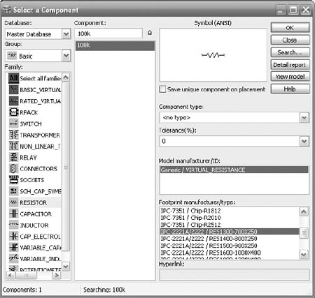
Figure 5.2: Selecting the resistors.
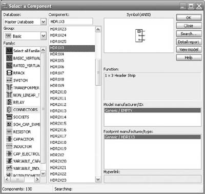
Figure 5.3: Selecting the headers.

Figure 5.4: Schematic drawing for the inverting amplifier with connection headers.
5.2.4 TRANSFERRING THE DESIGN TO ULTIBOARD
This step shows us how to transfer the design to Ultiboard. Depending upon the installed version available we should choose to send the design to Ultiboard version 11 or previous versions. This is done in the menu Transfer → Transfer to Ultiboard → Transfer to Ultiboard 11.
As a first requisite, Ultiboard asks for a file name. In this case, the file name is chosen as Example01_Inverting_Amplifier.ewnet. Note that Multisim creates a file with the extension ewnet. This is the file that Ultiboard uses to create the PCB. This launches the program and we see a window like the one shown on Figure 5.5. This is the import netlist which describes how the elements are connected in the circuit.
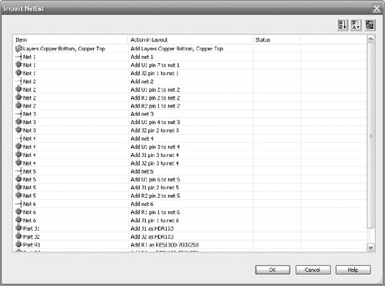
Figure 5.5: Import netlist.
As we can see in the main Ultiboard window, the tracks are 10 mils in width. This is the default width. We can change the units but the recommended units are mils. This is due to the fact that the vast majority of components are manufactured using mils as a reference, including the pin spacing of holes in a breadboard, so it is a safe procedure to work using the same units as the component packages we are using. From the menu Options → PCB Properties, the window for the PCB properties opens and in the Design rules tab we see the track width set at 10 mil. The recommended value when working with simple designs is 25 mils.

Figure 5.6: PCB properties. The Design rules tab is selected.
As the designs get progressively more complex, and therefore, more dense, the track width can be reduced to 10 mils or even less. The last parameter, clearances to trace is the minimum distance between contiguous tracks. The value of 10 mils is appropriate for our needs. Once we have imported the netlist we get the main window for Ultiboard, with the board outline and the imported components placed outside of the board (Figure 5.7).
We can zoom in and out with the mouse scroll wheel so we get a better view of the components and their connections. The yellow lines in Figure 5.8 are the imported nets; these allow the autorouter to know which component is connected to another one.
Here we can see the labels for each component; for example, J1 and J2 are two headers, U1 is the DIP8 integrated circuit and R1 and R2 are the resistors. The yellow lines, as we explained above, are the electric connections between elements; these come from the netlists and due to their entangled look they are sometimes called ratsnest.
In the View → Toolbars → Select menu we can activate the selection toolbar shown in Figure 5.9.
The first button enables the option for selecting components. When enabled we can drag components to any convenient location before routing. We can also enable the autoplacement function in the Autoroute toolbar but we must take into account that the results are not always what we are expecting. In this example we place the components as shown in Figure 5.10.
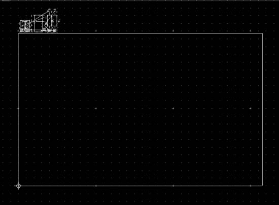
Figure 5.7: Initial placement of footprints in Ultiboard.
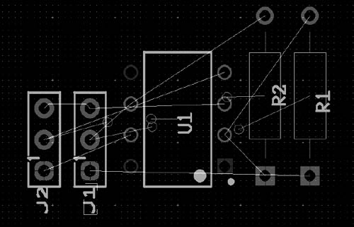
Figure 5.8: Zooming in to see a detailed view of the components.
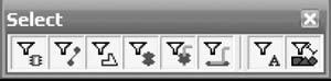
Figure 5.9: Selection toolbar.

Figure 5.10: Component placement before routing.
Now that the components are in place we can choose to use a manual placement of the tracks or the autorouting utility. First we see what happens with autorouting. The autorouter is invoked in the Autoroute → Start/Resume Autorouter menu. The results are similar to those shown in Figure 5.11.
As we can see, the results are very good. We could check to see that each connection is done properly to the corresponding pin in the IC.
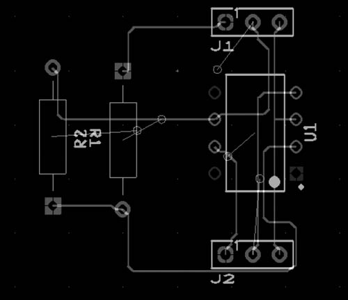
Figure 5.11: Autorouter results.
For a simple design the autorouter works well. For complex designs there is a high probability of tracks not being routed. In that case, we must manually draw the tracks.
Example 5.2 Signal conditioning for a digital thermometer based on LM35.
We are going to design a PCB for a digital thermometer based on the LM35 integrated circuit. This circuit has a TO-92 packaging typical of small-signal transistors. Its three terminals are VCC, GND and Vout. In its basic mode of operation we get 10 mV for each Celsius degree and it is capable of handling a temperature range of 0 to 100 °C.
We start with this range in mind and assume that we need to feed this voltage to another circuit that requires a range of 0 to 5 VDC, where 0 V is equivalent to 0 °C and 5V is equivalent to 100°C. This is a pretty common scenario in real life, where an analog signal is the source of a digital circuit that operates with TTL voltage levels.
The required signal conditioning involves a voltage gain of 5. We can then use an operational amplifier with a DIP8 packaging, for example a TL072. This circuit has the advantage that internally there are 2 independent op-amps and then we can use an inverting amplifier with a gain of 5 with a variable resistor for calibration and an inverter amp with unity gain for a positive output. The complete circuit can be seen in Figure 5.12.

Figure 5.12: Signal conditioning for an LM35 sensor.
Notice how we are using a 2N5088 BJT transistor instead of the LM35 sensor. This is done because they both share the same TO-92 packaging and there is no LM35 in the parts bin.
Again, we are going to transfer the design from Multisim to Ultiboard (from the Transfer → Transfer to Ultiboard → Transfer to Ultiboard 11 menu). Once we are running Ultiboard we are going to accept the default configuration and we have the components placed outside the board outline of our PCB.
With this default configuration we can make a test to see the results for a fully automated design. First, we need to autoplace the components (Autoroute → Start Autoplacement menu) and with that result we are going to try the autorouting feature (Autoroute → Start / Resume Autorouter). In our particular case we obtained 16 out of 17 tracks routed. This is a 94% of the whole design. In this basic design that means that we have to manually route one track or maybe use a wire jumper to make the connection. In a more complex design this could probably mean that we have to manually route dozens of tracks.
In this case, we can place a pair of vias on the board. Vias are connectors for going from one copper layer to another. Here we are going to use them in order to go from the copper top layer to copper bottom layer.
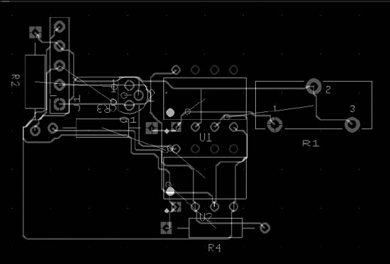
Figure 5.13: PCB connection using vias.
Here it is evident that there is a need for a mixture of routing and placement techniques. Each designer is going to develop his/her own set of techniques for the tracks that could not been routed by the software (see Figure 5.13).
In these examples we can see the design possibilities that Ultiboard offers. The next step in the PCB fabrication process is the electrical rules check. This is a check-up that can be run when a design is apparently finished; we can specify some criteria like distance between adjacent tracks and minimal width of tracks. This is useful when a design involves the use of RF (radio frequency) or high frequency signals.
In Ultiboard we can activate the Electric Rules Check by going to the menu Design → DRC and Netlists Check. If we check the design we have so far, we are hopefully not going to find any errors, but in more complex circuits it is always a good practice to periodically check for errors so we can fix them as they appear. This is going to save us a great deal of time in the long run.
If we wish to check the details or change the preferences for the electric rules, the menu we use is found under Options → PCB Properties → Design Rules.
A pair of interesting options that the Educational version of Ultiboard has are the PCB Transmission Line Calculator shown in Figure 5.14, and the PCB Differential Impedance Calculator shown in Figure 5.15. They are available in the menu Tools → PCB Transmission Line Calculator and Tools Tools → PCB Differential Impedance Calculator. Both are used for doing the calculations related to the electromagnetic values belonging to the material and dimensions used in our designs.
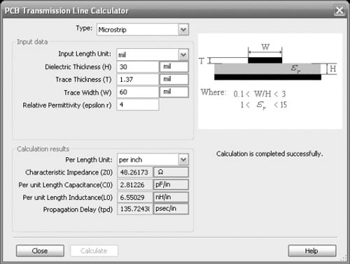
Figure 5.14: PCB Transmission Line Calculator.
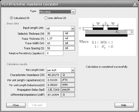
Figure 5.15: PCB Differential Impedance Calculator.
The final step in the process of making a PCB can be done using a number of very different techniques. For students making circuit prototypes it is very common to use techniques such as transferring with an iron, silkscreen or directly drawing the designs on the copper layer with a permanent marker.
For more complex designs, or designs involving two or more copper layers a quick alternative, but expensive, is the use of CNC (computer numerical controlled). These machines can make circuits with a high level of precision and practically with absolute repeatability.
Ultiboard allows us to take either route. For the simplest case the design can be printed on paper or in a number of transfer sheets available commercially. This is done under the menu File → Print and there we can select the desired size (a size of 100% is highly recommended when not using optical techniques like silkscreen), the printer, and the copper layers that we are going to print.
The procedure for the second case is different. We need to select the option File → Export and there we see a menu with different options for exporting files, among them SVG (Scalable Vector Graphics), Gerber and DXF (see Figure 5.16).
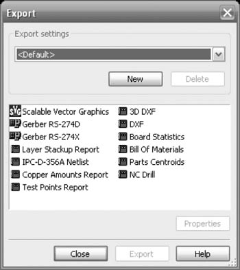
Figure 5.16: Export options.
If we select SVG, some design programs can handle very well the vector images obtained. As a suggestion you can use a free program called Inkscape that natively works with SVG files.
For Gerber files we need to specify which layers are going to be exported and after that define the aperture values. This is a value used by CNC machines for calculating the outline that should be routed when making the PCB. DXF export is similar with the difference that the user does not have to specify the apertures. DXF is a file type handled by CAD software.
5.4 CONCLUSIONS
In this chapter we have presented a few techniques for making PCBs using Multisim as a base for schematic capture and Ultiboard for designing the copper tracks.
We have also shown some variations on the basic techniques and the results that can be obtained. Finally, we listed the export options available so the user can choose the most appropriate for his/her needs.
REFERENCES
[1] D. Báez-López, F. E. Guerrero-Castro, Circuit Analysis with Multisim, Synthesis Lectures on Digital Circuits and Systems, Morgan and Claypool Publishers, Vol. 6, No. 3, 2011. Cited on page(s) 116
1 A mil is a thousandth of an inch.