Models and Subcircuits
Resistors, capacitors, inductors, diodes, and transistors are described in Multisim by a model. Other devices are rather described by a subcircuit.
A model is a description of the device by using its defining equations. Thus, a model can be built for any device whose equations are available from a theoretical analysis of its behavior and construction. Diodes and transistors are examples of circuit elements described by a model.
A subcircuit is a smaller circuit which can represent a set of specific properties of a larger circuit. Operational amplifiers and digital circuits such as flip-flops and gates are examples of circuits defined by subcircuits. A subcircuit is the equivalent of a method in object oriented programming and, thus, it can be reused whenever we require it.
Multisim libraries contain a great deal of parts defined by subcircuits. The definition of a subcircuit in the libraries is transparent to the user and can only be appreciated if we open the model for a device.
A user can modify a device model, can create a subcircuit to be used in a larger circuit, and can also create a subcircuit and make it available at either the Corporate or the User Database to be used by any circuit designed later on. In this section we present the procedures for the following:
1. Modify an existing element’s model.
2. Create a subcircuit within a larger circuit, and
3. Create a subcircuit and make it available at the database.
We show with three examples the procedures to accomplish these three tasks.
1.1 EDITING A COMPONENT MODEL IN MULTISIM
Multisim has the capability of editing components available in the Master Database. This is useful when we need to fit components to specific needs. For example, change the W/L ratio in an MOS transistor, the β in a BJT, the input impedance of an op amp, etc. There are two ways to edit components. The first method edits the component in such a way that they can be only used within the circuit where it was edited. It is not available for any other circuit simulation. The second method edits a component and then places it in the database for use in any other circuit simulation.
1.1.1 EDITING A COMPONENT FOR USE IN THE SAME CIRCUIT ONLY
We show this procedure with an example. In the example we edit the β of the transistor. Since the emitter resistor is missing, the amplifier is very sensitive to changes in β.
Example 1.1 Editing of BF in a common emitter amplifier.
Let us consider the common emitter amplifier shown in Figure 1.1. This circuit uses a 2N3904 bipolar transistor.
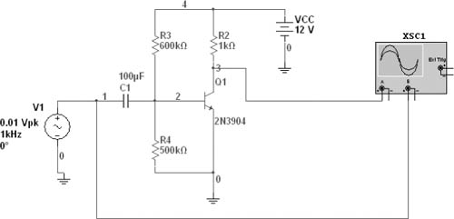
Figure 1.1: Common emitter amplifier.
From the oscilloscope window in Figure 1.2 we can see that the amplifier gain is given by:
![]()
Now, we edit the model for the 2N3904 bipolar transistor.
To edit this component we double click on the bipolar transistor 2N3904 to open the window of Figure 1.3. In this window we click on the Edit Model button to obtain the Edit Model window of Figure 1.4. In this window we see that the Bf = 416.4. We change this value to 50.0 and press enter. The new value is shown in Figure 1.5.
We now click on the Change Part Model to return to the window of Figure 1.3 and press the OK button. The circuit now looks as shown in Figure 1.6. We note an asterisk following the transistor number. This means that its model has been modified. We run the analysis again by pressing the Run button and take a look at the output shown in the oscilloscope as shown in Figure 1.7. We measure the voltage gain and it has changed to
![]()

Figure 1.2: Input and output waveforms for the common emitter amplifier.
which is less than the value obtained in the case of β = 416.4 where we used the original value for β.
1.1.2 EDITING A COMPONENT IN THE DATABASE
Multisim has all the components grouped in databases. The available databases are the following: the Master database, the Corporate database, and the User database. We can only edit components in the Corporate and the User databases. Thus, if we wish to edit a model in the Master database, we have first to copy the component to any of the other two databases.
Example 1.2 Copying a component from the Master Database to either the Corporate or User database.
In this example we want to copy a component from the Master database to the User database. We use the transistor 2N3904 from Example 1.1. In this circuit, or in any circuit with the transistor, we select it and then we select Tools→Database→Save Component to Database. This opens the dialog window shown in Figure 1.8. We select the User Database and the transistors family as shown in Figure 1.9.
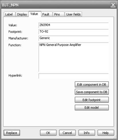
Figure 1.3: Dialog window for the bipolar transistor.
Then we click on the Add family button and the dialog window shown in Figure 1.10 opens. There we change the default name Def to Bipolar, as is shown in the figure. We press the OK button. This closes the window and it returns to the Select Destination Family window, and the new family group is displayed, as shown in Figure 1.11. When we click on the OK button, a message indicates the successful copying of the element to the target database and the window is closed, and the Database Manager window shown in Figure 1.12 is open, showing the User Database with the transistor 2N3904 as the only element available in the database. We are now ready to edit this transistor and change its parameters.
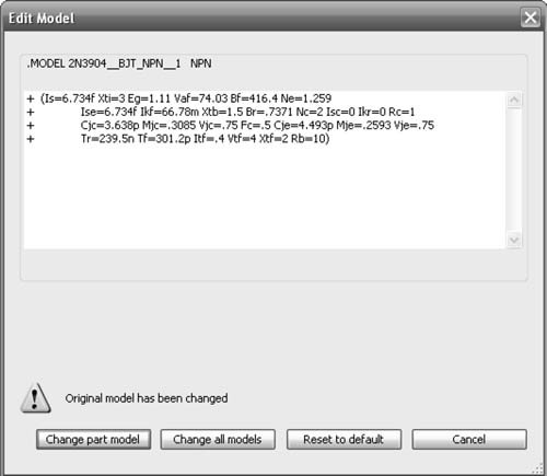
Figure 1.4: Edit model window for the 2N3904.
Example 1.3 Editing the 2N3904 bipolar transistor model in the User database.
We continue with Example 1.2. Here we are going to modify the β of the transistor and then we test the changes in the common emitter amplifier from Example 1.1. In order to do so we have to modify the model of the bipolar transistor 2N3904. To achieve our goal we have to complete the following steps.
1. To edit the model we select Tools→Database→Database Manager to obtain the window in Figure 1.14. This figure is identical to Figure 1.12 because is the same component we have not added new components. If there are more components in the database, we look for the required component. Once this is done we press the Edit button. This opens the Component Properties window of Figure 1.15. There we see that the value for the parameter Bf is 416. To edit the model we press on the Add/Edit button which opens the dialog window of Figure 1.16.
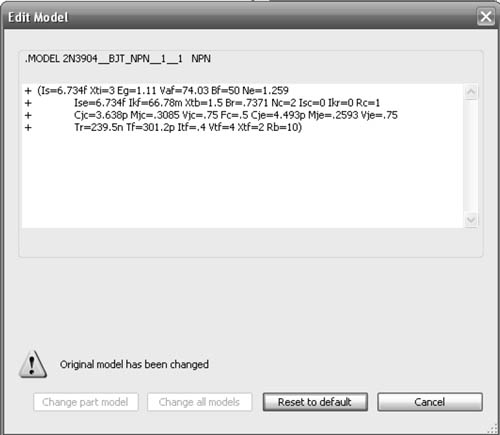
Figure 1.5: Change of the parameter Bf to Bf = 50 for the 2N3904.
We proceed to make the desired changes. In this example we wish to change Bf from its nominal value of 416.4 to the desired value of 85, as shown in Figure 1.17. We press the Select button in the same window and Multisim warns us that the model has changed and if we wish to proceed, as shown in Figure 1.18 and then, after clicking the OK, Multisim takes us to the window of Figure 1.19 where we press the Overwrite button. This opens the Select a Model window of Figure 1.20 which shows the model for our component.
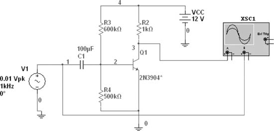
Figure 1.6: Transistor with Bf = 50.
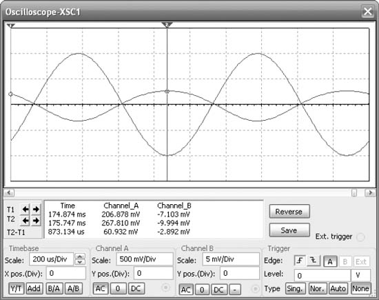
Figure 1.7: Input and output waveforms for amplifier with BF=50. The gain has decreased because BF has decreased.
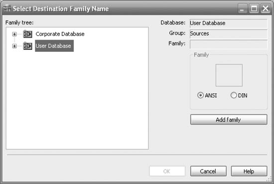
Figure 1.8: Dialog window to select the destination database.
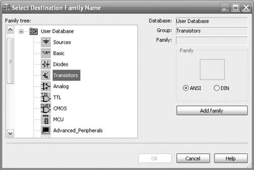
Figure 1.9: Expansion of the User database with the Transistors family selected.
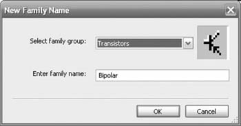
Figure 1.10: Here we name the new family group.

Figure 1.11: Expansion of the User database with the new family displayed.
If we wish to rename the component, we can do it in the Component Properties window. This window can be open by double clicking on the transistor. This opens the window for the component (see Figure 1.3) and we click on the Edit Component in DB which opens the Component Properties window. There we can change the name as desired. We wish to change the model’s name to 2N3904_new, as shown in Figure 1.21.
This takes us to the Select Destination Family Name window as it was done before. When we are finished, we are ready to simulate circuits with this new component.

Figure 1.12: Elements in the User Database. Only the transistor 2N3904 is displayed.

Figure 1.13: Message indicating the successful copy to the User Database.

Figure 1.14: Database Manager with the Components tab for the User Database.
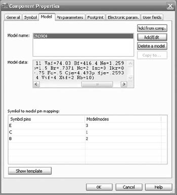
Figure 1.15: Component Properties for the selected component.
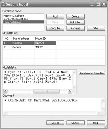
Figure 1.16: Dialog window to edit the model of the 2N3904.
We could also have renamed the component if after changing the desired parameters, in Figure 1.17 we press the Rename key and this takes us to the window shown in Figure 1.22 where we enter the new name.
Example 1.4 Common emitter amplifier with low β model.
We replace the BJT in the circuit of Example 1.1 with the transistor 2N3904_new (see Figure 1.23) and run the analysis to obtain the input and output waveforms of Figure 1.24. Here the smaller amplitude signal is the output. Measuring the gain we see that the new gain is now
![]()
This is a considerable reduction in gain. The considerable loss in gain is due mainly to the absence of an emitter resistor which is used to reduce the effects of β variation in the transistor Q point [1].
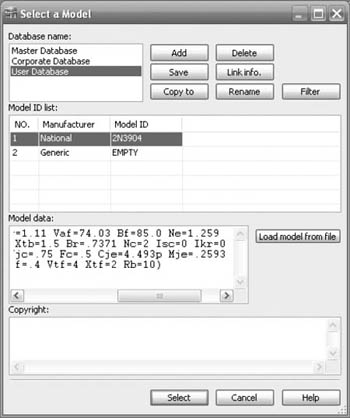
Figure 1.17: Dialog window to edit the model of the 2N3904.
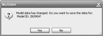
Figure 1.18: Dialog window to save the changes to the model.

Figure 1.19: Dialog window to overwrite the model after the changes are made.

Figure 1.20: The parameter BF has been changed to 85 for the 2N3904.
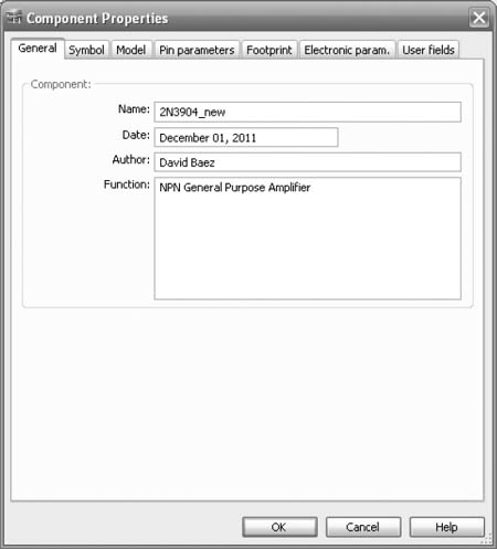
Figure 1.21: Component’s model name has been changed to 2N3904_new.
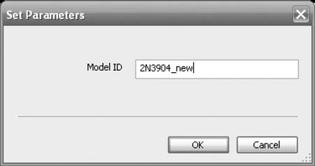
Figure 1.22: Component’s model name has been changed to 2N3904_new.
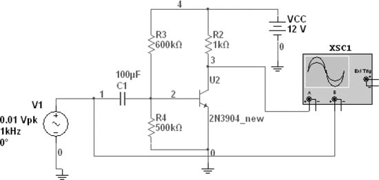
Figure 1.23: Common emitter amplifier with new transistor from the User Database 2N3904_new which has Bf = 54.
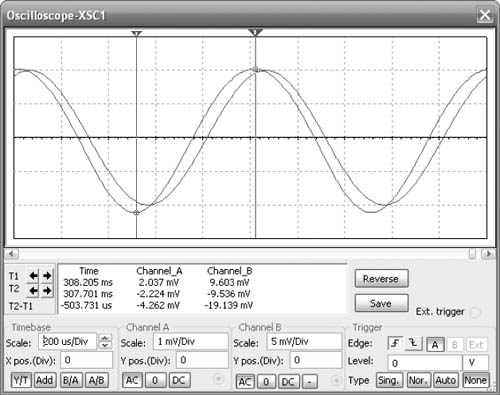
Figure 1.24: Input and output waveforms for the common emitter amplifier. The output voltage is much less than in the Example 1.1.
1.2 CREATING SUBCIRCUITS IN MULTISIM
The use of subcircuits enhances the capabilities of circuit simulation. By using subcircuits we can create new components not provided in the databases. Subcircuits are useful when there is a circuit portion which repeats several times in a larger circuit. Thus, a larger circuit can be divided into smaller modules facilitating its diagram description. Multisim users can create subcircuits by using the Component Wizard provided in the main menu. There are two methods to create subcircuits. The first method creates a subcircuit to be used only in the circuit where it was created. In this case, a set of parts can be grouped together for reuse within the same circuit. The second method creates a subcircuit that can be kept in the Database for use in any other circuit simulation. In this case, we can create a part for a subcircuit provided by a vendor. We show all of these procedures with examples.
Example 1.5 Subcircuit for use within a circuit.
Let us consider the circuit of Figure 1.25. This is an RC-active KHN filter using three operational amplifiers [2]. The first operational amplifier is a summing amplifier while the last two are Miller integrators. The first integrator is formed by C2, R4, and U2. The second integrator is composed by C1, R6, and U3. If the output is taken from the first integrator’s output, then the frequency response is that shown in Figure 1.26. It shows that the circuit realizes a band pass filter. We can group each of the integrators within a subcircuit. We do this by selecting the portion of the circuit as shown in Figure 1.27.
Now, from the main menu select Place→Replace by Subcircuit (Figure 1.28). This opens the dialog window shown in Figure 1.29 requesting a name for the subcircuit. After clicking on the OK button, Multisim asks if the merging of the nodes in the subcircuit and in the circuit is correct. We click on the OK button as many times as it is requested. When we are finished, the window shown in Figure 1.31 opens. Here we edit the subcircuit. We click on the Edit HB/SC button. The circuit inside the subcircuit block is open, as shown in Figure 1.32. We edit the circuit as needed, save it, and close the editor page. The edited circuit appears in Figure 1.33.
The final circuit using subcircuit blocks for both integrators in the filter is now ready for simulation. We perform an AC analysis to obtain the frequency response shown in Figure 1.35 which agrees with the one obtained in Figure 1.26
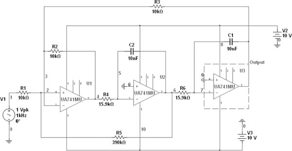
Figure 1.25: Active-RC KHN filter.
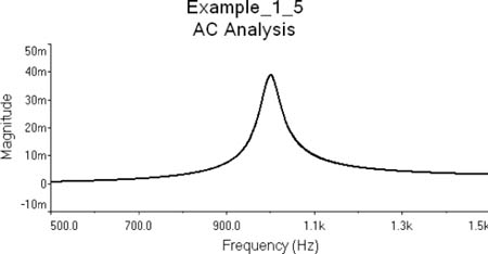
Figure 1.26: Frequency response showing the bandpass response.
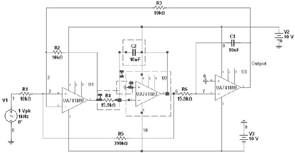
Figure 1.27: Portion of the filter selected for the subcircuit.
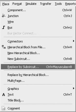
Figure 1.28: Path for the subcircuit creation.
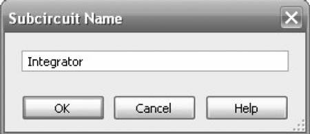
Figure 1.29: We here give the name for the subcircuit.
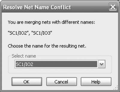
Figure 1.30: Choosing the names for the subcircuit pins.
1.2.1 SUBCIRCUIT TO BE LOCATED IN THE DATABASE
In this section we present with an example the procedure to create a subcircuit from a node description of the circuit. We use the Component Wizard to create the subcircuit.
Example 1.6 Subcircuit for an operational amplifier macromodel available in the database. In this example we create a subcircuit block for the operational amplifier macromodel of Figure 1.36.
The circuit description in terms of the connections at nodes 1, 2, 3, Vin+, Vin-, and Vout is:
Rin VIN+ VIN- 2MEG
Epole 1 0 VIN+ VIN- 200000
Rpole 1 2 1k

Figure 1.31: Dialog window to edit the subcircuit.

Figure 1.32: Schematic diagram for the subcircuit before deleting unneeded pins.

Figure 1.33: Subcircuit final schematic diagram.
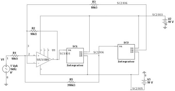
Figure 1.34: KHN filter with integrator subcircuits.

Figure 1.35: Frequency response for the filter using the subcircuit.

Figure 1.36: Macromodel for an operational amplifier.
Cpole 2 0 15.92u
Eout 3 0 2 0 1
Rout 3 OUT 300
where the component name is given first, the nodes where the component is connected follow, and finally the value. For the VCVS Epole, which describes the dominant pole, and Eout, which gives the low output impedance, we need, after the first two node names, the nodes where the VCVS takes is value, and finally the gain.
The procedure starts by selecting from the main menu Tools →Component Wizard which opens the dialog window of Figure 1.37. In this window we provide subcircuit information such as the component name, author’s name, component type from among Analog, Digital, Verilog_HDL, or VHDL. Finally, we briefly describe the function realized by the subcircuit. We can see that this is the first window out of either 8, 7 or 6. The number of steps required in the subcircuit creation process depends upon the option we select in the radius buttons in this dialog window. For our example we select Simulation only (model) which needs 7 steps.
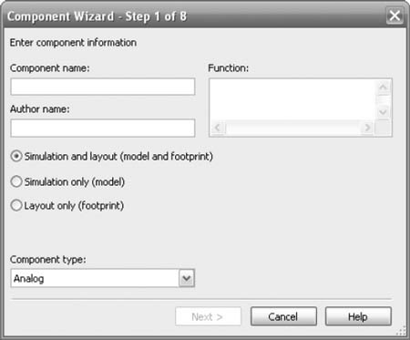
Figure 1.37: Dialog window for the Component Wizard.
We provide then the following information:
Component type name: |
UDLAP_741 |
Author Name: |
Baez_Guerrero_Cervantes |
Component Type: |
Analog |
Function: |
Op-amp single pole macromodel. |
We select the radius button for: Simulation only (model). The window with the data is shown in Figure 1.38. We then press Next and obtain the second window for the Component Wizard, shown in Figure 1.39.
In this second window we select the radius button for: Single Section Component. This indicates that the part only has a macromodel. If the part has two or more macromodels, we select the button: Multi-Section Component. This is the case of TTL digital circuits where there are usually more than one circuit in the package. We also select 3 as the number of pins since we have two inputs and one output. Then, we click on the Next button. The window of Figure 1.40 is displayed now.
In this step we edit the subcircuit symbol. Although we can edit the symbol with the Symbol editor, it is better if we start from a known circuit symbol from the Database. Since we are creating an op amp subcircuit, we can use one from the Multisim Master Database. Thus, we click on the Copy from DB button to arrive at Figure 1.41. Here we can select a symbol by going to the appropriate library and we select either a component with the required symbol or a symbol looking closer to what we need. We select the Analog library and look for any op amp. We choose the op amp LM308M and press the OK button and we are returned to the previous window which now presents the symbol chosen (see Figure 1.42).

Figure 1.38: First dialog window for Component Wizard with data for the macromodel.

Figure 1.39: Second dialog window for Component Wizard.
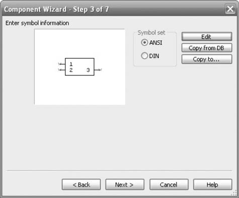
Figure 1.40: Component Wizard window No. 3 to edit the subcircuit symbol.
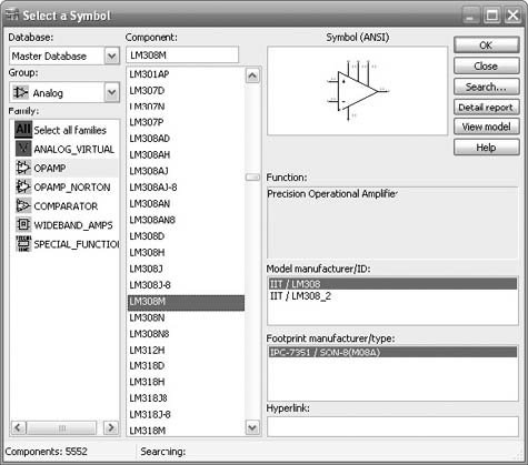
Figure 1.41: Choosing the symbol for the op amp macromodel.
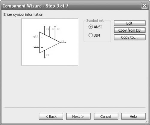
Figure 1.42: Window with the chosen symbol to edit.
We are now ready to edit the symbol to fit our requirements. We now press the Edit button. This takes us to the Symbol Editor shown in Figure 1.43.
The Symbol editor has toolbars which allows adding or deleting components in the circuit symbol. We can also delete rows from the spreadsheet at the bottom of the Symbol editor. After deleting the lines and pins that we do not need we get to the circuit symbol of Figure 1.44. We save the changes and close the Symbol Editor window to get to the window of Figure 1.45. If we are satisfied with the symbol, we press the Next button to arrive at Figure 1.46a where we select the pin function from the several options available for each pin, namely, bidirectional, unidirectional, input, output, and power. For the input pins we select INPUT and for the output pin we select OUTPUT as shown in Figure 1.46b.
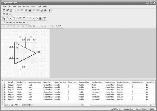
Figure 1.43: Symbol editor window.

Figure 1.44: Subcircuit symbol.
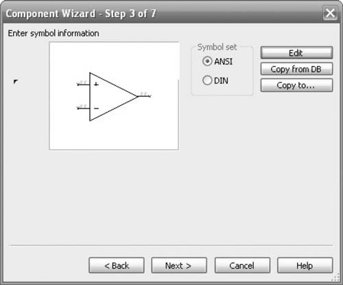
Figure 1.45: Subcircuit final symbol.
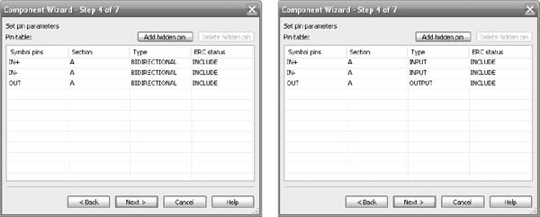
Figure 1.46: Selection of pin description.

Figure 1.47: Window to write the subcircuit description.
Pressing the Next button we get to step 5 of the Component Wizard shown in Figure 1.47. In this window we write the model name and the circuit description, as shown in Figure 1.48. We use the netlist that describes the macromodel and we have added the row:
.SUBCKT UDLAP_741 vin+ vin- out
This row indicates that the circuit description is a subcircuit with the name UDLAP_741. The three variables vin+, vin-, and out are the three pins to the subcircuit and they must always be given in this order. There are three rows that start with an asterisk. These are comment rows and do not affect the macromodel. There is also a row with .ENDS which indicates the end of the subcircuit description. When we are finished, we press the Next button to get to Figure 1.49 that describes the mapping information between the symbol pins and the model nodes. If we agree with that description, we click on the Next button.
Finally, we get to the Component Wizard window shown in Figure 1.50. In this window we select the Database; in our example we select the User Database. We also select the family; in this example we choose the Analog group and add the family AO. This part of the process is similar to the one shown in Example 1.5. We click on the finish button and this ends the subcircuit creation procedure.
We can check the existence of the new part if we select the components in the User Database in the Analog group and the family AO, as shown in Figure 1.51.
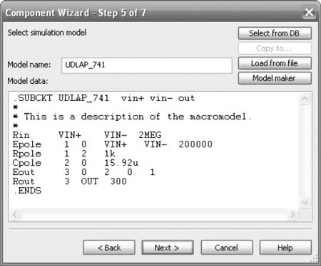
Figure 1.48: Subcircuit description for the Op amp UDLAP_741.

Figure 1.49: Pin assignment.

Figure 1.50: Subcircuit description.
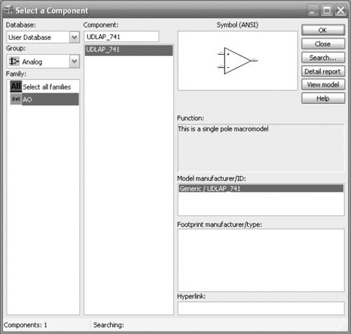
Figure 1.51: Subcircuit UDLAP_741 in the User Database.
Example 1.7 Inverting amplifier using the 741_UDLA op amp.
To test the macromodel, we wire up an inverting amplifier with a gain of -10 as shown in Figure 1.52. We perform a transient analysis from 0 to 2 msec. The variables we wish to plot are the input voltage V1 and the output voltage V3, as shown in Figure 1.53. After the transient analysis is done we obtain the plots of Figure 1.54 where the gain is -10, as expected.

Figure 1.52: Inverting amplifier.

Figure 1.53: a) Transient analysis specifications and b) variables to plot.
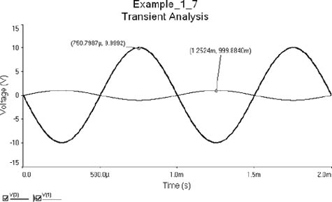
Figure 1.54: Inverting amplifier transient response.
1.3 CONCLUSIONS
An important part of the simulation is the modelling of each of the circuit components. In this chapter we have learned how to modify existing models, so they are suitable with a designer particular needs. We have also covered the way a subcircuit is created. Subcircuits are useful whenever either a circuit is repeated or it is going to be used as a module. We have also covered the way schematic symbols.
1.4 PROBLEMS
1.1. The inverter circuit in Figure 1.55 uses NMOS transistors. Use the model shown below for them. Test the circuit with a square signal. (The + sign at the beginning of a row a indicates continuation row.)
.MODEL CMOSN NMOS LEVEL = 2 PHI = 0.600000 TOX = 4.3500E-08
+ XJ = 0.2U TPG = 1 VTO = 0.8756 DELTA = 8.5650E+00 LD = 2.395E-07
+ KP = 4.5494E-05 UO = 573.1 UEXP = 1.5920E-01 UCRIT = 5.9160E+04
+ RSH = 1.0310E+01 GAMMA = 0.4179 NSUB = 3.3160E+15 NFS = 8.1800E+12
+ VMAX = 6.0280E+04 LAMBDA = 2.9330E-02 CGDO = 2.8518E-10
+ CGSO = 2.8518E-10 CGBO = 4.0921E-10 CJ = 1.0375E-04 MJ = 0.6604
+ CJSW = 2.1694E-10 MJSW = 0.178543 PB = 0.800000
* Weff = Wdrawn - Delta_W
* The suggested Delta_W is -4.0460E-07
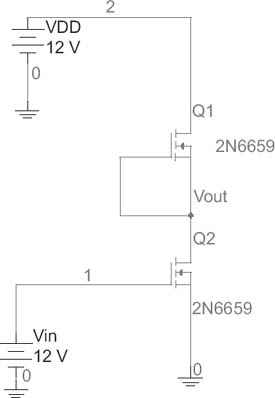
Figure 1.55: NMOS inverter circuit.
1.2. MOSIS provides models for diodes and transistors in different processes. The page is www.mosis.com. Test the inverter circuit in Example 1.1 with transistors with 0.5 microns process.
1.3. Test an inverter 7404 TTL by changing the rise and fall time to 10 msec.
1.4. The netlist below belongs to the TLC2201 op amp macromodel. Create a part for this circuit and store in a family group in the MISC group. Build a non-inverting amplifier with a gain of +10. Use 9KΩ and 1KΩ resistors.
* TLC2201 OPERATIONAL AMPLIFIER “MACROMODEL” SUBCIRCUIT
* CREATED USING PARTS RELEASE 4.03 ON 08/06/90 AT 15:18
* REV (N/A) SUPPLY VOLTAGE: 5V
* CONNECTIONS: NON-INVERTING INPUT
* | INVERTING INPUT
* | | POSITIVE POWER
* | | | NEGATIVE POWER SUPPLY
* | | | | OUTPUT
.SUBCKT TLC2201 1 2 3 4 5
*
C1 11 12 11.00E-12
C2 6 7 50.00E-12
DC 5 53 DX
DE 54 5 DX
DLP 90 91 DX
DLN 92 90 DX
DP 4 3 DX
EGND 99 0 POLY(2) (3,0) (4,0) 0 .5 .5
FB 7 99 POLY(5) VB VC VE VLP VLN 0 537.9E3 -50E3 50E3 50E3 -50E3
GA 6 0 11 12 282.7E-6
GCM 0 6 10 99 2.303E-9
HLIM 90 0 VLIM 1K
ISS 3 10 DC 125.0E-6
J1 112 10 JX
J2 12 1 10 JX
R2 6 9 100.0E3
RD1 60 11 3.537E3
RD2 60 12 3.537E3
RO1 8 5 188
RO2 7 99 187
RP 3 4 5.71E3
RSS 10 99 1.600E6
VAD 60 4-.5
VB 9 0 DC 0
VC 3 53 DC .928
VE 54 4 DC .728
VLIM 7 8 DC 0
VLP 91 0 DC 2.800
.MODEL DX D(IS=800.0E-18)
.MODEL JX PJF(IS=500.0E-15 BETA=1.279E-3 VTO=-.177)
.ENDS
REFERENCES
[1] A.S. Sedra and K.C. Smith, Microelectronic Circuits, Holt, Rinehart, and Winston, New York, 2005. Cited on page(s) 12
[2] L.P. Huelsman, Introduction to the Theory and Design of Active and Passive Filters, McGraw-Hill Co., New York, 1991. Cited on page(s) 17