
Energetic and Nanostructural Design of Small-Molecular-Type Organic Solar Cells
MASAHIRO HIRAMOTO
Department of Materials Molecular Science, Institute for Molecular Science, National Institutes of Natural Sciences, 5-1 Higashiyama, Myodaiji, 444-8787, Okazaki, Aichi, Japan
Contents
- I. Introduction
- II. History
- III. Principles
- IV. Nanostructure Design
- V. Energetic Structure Design
- VI. Conclusion
- Acknowledgments
- References
I. Introduction
One of the responsibilities of scientists is to help to develop new ways in which we can generate energy, since gaining control over energy resources such as petroleum has been one of the main reasons for conflict between nations. Renewable energy generated by solar cells is one of the potential solutions to the problem of maintaining our energy supply, and these have been studied intensively for about half a century. Today, silicon solar cells have already been commercialized and have become an indispensable source of electricity. However, the price of electricity produced by silicon solar cells is still higher than that produced by petroleum. In order to increase the production of energy by solar cells, the price of electricity produced by solar cells needs to be lower than that of electricity produced by petroleum. Organic solar cells have the potential to be part of the next generation of low-cost solar cells. There was a steep increase in the power-conversion efficiency of organic solar cells around the year 2000 (Fig. 1), indicating that the technology needed to bring them to a commercial level would be established by around 2020, taking into consideration the example of organic electroluminescent devices for which scientific breakthroughs were made in 1987 and commercialization occurred around 2010. Now, in 2016, the power-conversion efficiency of organic solar cells has reached 12%.

Figure 1 The history of organic solar cells. The main breakthroughs are indicated by arrows. The efficiencies after the year 2000 (closed circles) are plotted according to the NREL chart. Open circles are plotted according to recent press releases.
Organic solar cells have many advantages; they are flexible, printable, light-weight, low-cost, can be fashionably designed, and can be fabricated by roll-to-roll production, and so on. Printed organic solar cells can be attached to the roofs, windows, and walls of houses and buildings. Automobiles can be fabricated and wrapped with colorfully printed organic solar cells. Moreover, they are suitable for constructing solar power plants in space, since their light-weight allows them to be easily put into orbit. A flexible see-through organic solar cell module and a demonstration building using these modules as exterior walls and windows are shown in Fig. 2.
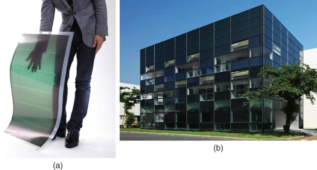
Figure 2 (a) Commercial flexible see-through organic solar cell module (Mitsubishi Chemical Corporation). (b) Building using these modules on the exterior walls and windows.
In this chapter, the history, principles, and energetic and nanostructural designs for small-molecular-type organic solar cells are summarized.
II. History
The first organic solar cell was fabricated by Calvin in 1958 (Fig. 1) [1]. For a long while, single films of small-molecule organic semiconductors deposited by vacuum evaporation were used. Typical organic semiconductors were phthalocyanines [2] and merocyanine [3]. Most organic semiconductor films had p-type characteristics, since oxygen molecules from the ambient air inevitably doped the films, acting as acceptors. A photocurrent could be generated at the Schottky junctions between the p-type organic films and a low-work function metal, such as Al. However, in the early stages of development, organic solar cells generated little photocurrent, typically less than several microamperes [4, 5].
A breakthrough occurred in 1986, namely, the development of a two-layer organic photovoltaic cell, which had a high photocurrent density (of the order of mA/cm2) and an efficiency of 1% (Fig. 1). This came about as a result of the donor/acceptor sensitization reported by Tang [6], which has had a big impact in the field of organic solar cells. A blended junction for small-molecule cells was proposed in 1991 by Hiramoto et al. [7, 8]. In 1993, Sariciftci et al. [9] reported a polymer heterojunction cell, which was followed in 1994 by a bulk polymer heterojunction cell reported by Yu et al. [10]. Typical combinations of donors and acceptors for small-molecular systems, which appear in this chapter, are shown in Fig. 3. Based on these fundamental studies, after 2000, the efficiency rose from 1% and started to increase rapidly and reached 12% by 2013. Nowadays, the photocurrent density of organic solar cells induced by solar radiation is approaching 20 mA/cm2, which is comparable to the values produced by inorganic solar cells.

Figure 3 Chemical structures of typical organic semiconductors acting as donors and acceptors that appear in this chapter.
III. Principles
A. Excitons
The dissociation of photogenerated electron–hole pairs (excitons) is a key factor for generating carriers in organic semiconductors. Exciton dissociation is affected by the relative permittivity of the solid (ϵ). The attractive force between an electron–hole pair is given by Coulomb's law.
Here, ϵ0, q1, q2, and r are the absolute permittivity, the elementary charges on the electron and the hole, and the distance between them. In a solid with a small value of ϵ, the positive and negative charges experience a strong attractive force, whereas, in a solid with a large value of ϵ, the positive and negative charges experience a relatively weak attractive force. Inorganic semiconductors have large values for ϵ. For example, the value for Si is 11.9, and the exciton has a large diameter of 9.0 nm and is localized over about 104 Si atoms (Fig. 4(a)). The thermal energy at room temperature is sufficient for this Wannier-type exciton to dissociate immediately into a free electron and a hole, thereby generating photocurrent. On the other hand, organic semiconductors have small values for ϵ. For example, the value for C60 is 4.4, and the exciton diameter is just 0.50 nm and is localized over a single C60 molecule (Fig. 4(b)). The thermal energy at room temperature is hardly sufficient for these Frenkel-type excitons to dissociate into free electrons and holes, and they can easily relax into the ground state (Fig. 5(a)). Therefore, organic semiconductors generate few photocarriers. This is the reason why organic solar cells fabricated before the work of Tang [6] had extremely low photocurrents, of the order of less than a microampere.

Figure 4 Size of excitons for an inorganic semiconductor (Si) (a) and an organic semiconductor (C60) (b). The former is a Wannier-type and easily dissociates into free carriers. The latter is a Frenkel-type and dissociates into free carriers with difficulty.
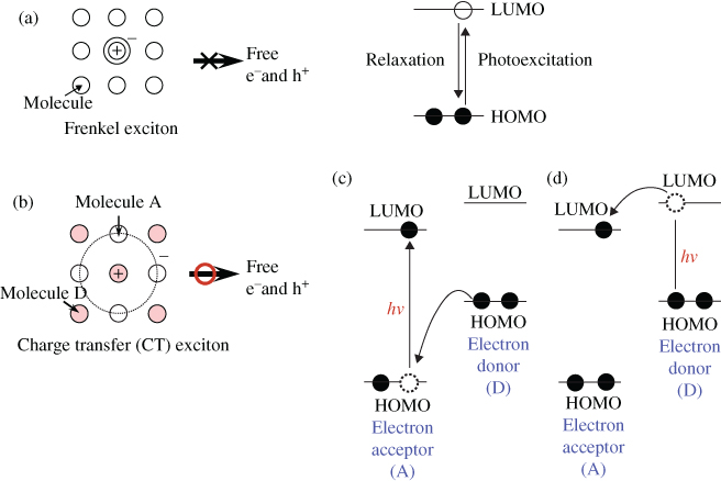
Figure 5 Carrier generation in organic semiconductors. (a) Single molecule solids. (b) Donor (D)/acceptor (A) sensitization for carrier generation by mixing two kinds of organic semiconductor molecules. Efficient free carrier generation occurs from the charge transfer (CT) exciton. (c) Photoinduced electron transfer from the HOMO of the donor molecule (D) to the HOMO of the acceptor molecule (A). (d) Photoinduced electron transfer from the LUMO of the donor molecule (D) to the LUMO of the acceptor molecule (A).
B. Donor–Acceptor Sensitization
Today's organic solar cells have overcome the aforementioned problem by combining two kinds of organic semiconductor. An electron-donating molecule (D) and an electron-accepting molecule (A) for which the energetic relationship of the highest occupied molecular orbital (HOMO) and the lowest unoccupied molecular orbital (LUMO) are brought together in contact or blended. When the electron-accepting molecule (A) is excited, electron transfer from the HOMO of the electron-donating molecule (D) to the HOMO of the electron-accepting molecule (A) occurs, and as a result, the A molecule charges negatively (A−), and the D molecule charges positively (D+) (Fig. 5(c)). On the other hand, when the electron-donating molecule (D) is excited, electron transfer from the LUMO of the electron-donating molecule (D) to the LUMO of the electron-accepting molecule (A) occurs, and as a result, the A and D molecules charge negatively (A−) and positively (D+), respectively (Fig. 5(d)). Irrespective of the excitation of molecules (A) and (D), the charge transferred states (D+A−) that are obtained are the same. Thus, a charge transfer (CT) exciton is formed in which the positive and negative charges are separated on neighboring D and A molecules due to photoinduced electron transfer (Fig. 5(b)). This CT exciton can dissociate to a free electron and a hole due to thermal energy at room temperature. By utilizing this donor–acceptor (D/A) sensitization, organic semiconductors have become capable of generating photocurrents of significant magnitude, of the order of milliamperes, induced by solar radiation.
C. Exciton Diffusion
A two-layer organic solar cell (Fig. 6) [6] utilizes D/A sensitization at the heterojunction. The width of the photoactive region (shaded region) is, however, limited to around 10 nm in the vicinity of the heterojunction due to the extremely small exciton diffusion length of just several nanometers [11, 12]. So, when the thicknesses of the organic layers are increased, the so-called “masking effect” occurs, namely, a dead region develops in front of the active region in which the incident solar light is absorbed and no photocurrent is generated, and as a result, the magnitude of the photocurrent is severely suppressed. A 10-nm-thick organic film can only absorb a small part of the incident solar light. However, in order to increase the efficiency of organic solar cells, it is necessary for the whole of the incident solar light to be absorbed in the 10-nm-thick active layer. Estimation of the exciton diffusion length is discussed in Section III.A.

Figure 6 Schematic illustration of a two-layer cell composed of perylene pigment (Im-PTC) acting as an acceptor molecule (A) and copper phthalocyanine (CuPc) acting as a donor molecule (D). Photocurrent is generated only in the active region (shaded) close to the heterojunction, and all other parts of the organic films act as dead regions.
D. Blended Junctions
In order to overcome this problem, blended junctions, which contain both donors and acceptors, were fabricated in organic semiconductors using a co-deposition technique for small-molecule organic solar cells (Fig. 7(a)) [7, 8]. From the standpoint of photocarrier generation occurring at the molecular level, there are donor/acceptor molecular contacts that act as photocarrier generation sites due to donor/acceptor sensitization in the bulk of the co-deposited layer. Blended junctions, so-called “bulk heterojunctions,” have become crucial for polymer organic solar cells [10].

Figure 7 (a) A small-molecule cell consisting of blended junctions in an organic semiconductor, containing both donor and acceptor molecules. The entire bulk of the blended layer acts as an active layer for photocarrier generation. (b) Energetic structure of a blended junction in a small-molecule cell.
Blended junctions are physically fundamentally the same as the porous TiO2 in the dye-sensitized solar cells proposed by Grätzel in 1991 [13]. For both solid/solid and solid/electrolyte junctions, by transmitting the incident light through a vast number of heterointerfaces, the whole of the incident solar light can be absorbed in extremely thin active layers.
Figure 7(b) shows the energetic structure of the blended junction in a small-molecule cell. Photogenerated electrons in donor molecules transfer from the LUMO of the donor molecule to that of the acceptor molecule and photogenerated holes in acceptor molecules transfer from the HOMO of the acceptor molecule to that of the donor molecule. This D/A sensitization promotes photocurrent generation. The original concept is that the positive and negative charges from ionized donors and acceptors in n- and p-type organic semiconductors, respectively, are compensated by each other, and the resulting co-deposited interlayer behaves like an intrinsic semiconductor [8]. With regard to the formation of the built-in potential in a molecular solid, the built-in electric field is distributed across an i-interlayer sandwiched between n- and p-layers, similar to the case of amorphous silicon incorporating a p–i–n junction.
IV. Nanostructure Design
Even if exciton dissociation occurs, nanostructure-control of the co-deposited films, that is, route-formation for electrons and holes generated by exciton dissociation, is crucial in order to extract a significant portion of the photogenerated charge to the external circuit. Once the two kinds of organic semiconductors that will act as donor and acceptor layers are blended, extraction of photogenerated holes and electrons inevitably becomes a tough problem, since they can only move through the electron-accepting molecules (A) and the electron-donating molecules (D).
A. Vertical Superlattices
An ideal nanostructure is the “vertical superlattice” (Fig. 8(a)). This structure enables the efficient dissociation of photogenerated excitons at the D/A interfaces within the exciton diffusion length (5–10 nm) and the transport of electrons and holes to the respective electrodes.

Figure 8 (a) Vertical superlattice structure. (b) Co-evaporant third molecule introduction. The balls, plates, and sticks correspond to C60, H2Pc, and third molecules, respectively. Matsuo et al., 2009 [14]. Reproduced with permission of American Chemical Society. Cross-sectional SEM images of C60:H2Pc co-deposited films without (c) and with (d) third molecule. Matsuo et al., 2009 [14]. Reproduced with permission of American Chemical Society. (e) Interdigitated structure of round columns of crystalline benzoporphyrin (BP) with diameters of around 20 nm standing almost vertically, used in highly efficient cells.
Matsuo et al., 2009 [14]. Reproduced with permission of American Chemical Society.
In this section, the characteristics of intentionally designed vertical organic superlattice structures are discussed [12]. In the vacuum deposition of an alternating multilayered structure of two kinds of materials, each film layer has to be deposited in sequence on the substrate (Fig. 9(a)). The thicknesses of the layers can be controlled with angstrom-order precision by monitoring with a quartz crystal microbalance (QCM), in the film thickness direction only. Here, if we consider rotating the multilayered film by 90° and making it vertical with respect to the substrate and having the cross-section of the multilayered film as the exposed surface (Fig. 9(b)), then control of the structures in the direction parallel to the surface on a nanometer scale is possible by controlling the deposition film thickness.

Figure 9 (a) Multilayered film and (b) vertical multilayered film.
Reprinted with permission from Hiramoto [15]. Copyright© 2006 Wiley Periodicals, Inc.
From the standpoint of photoelectric conversion, when a vertical superlattice structure (Fig. 8(a)) consisting of alternating perylene pigment (Me-PTC, Fig. 3) layers acting as acceptor molecules and metal-free phthalocyanine (H2Pc, Fig. 3) layers acting as donor molecules is exposed to light, efficient charge separation occurs at the interface of the donor/acceptor organic semiconductors and the photogenerated electrons and holes are transported such that they are spatially separated.
The fabrication method is shown in Fig. 10. A substrate having a flat surface was made using an epoxy resin. Me-PTC and H2Pc were deposited alternately on the substrate by vacuum evaporation. The multilayered film was embedded using the same epoxy resin as the substrate. By using a microtome (Leica, ULTRACUT UCT) equipped with a diamond knife (Diatome Ltd), the embedded film could be sliced perpendicular to the film surface. Epoxy film containing an embedded vertical superlattice having a height of 2 µm in the center was obtained. Finally, silver electrodes were deposited on both sides of this epoxy film. The completed cell has a structure consisting of a vertical multilayered film with height of 2 µm sandwiched by Ag electrodes (Fig. 8(a)).
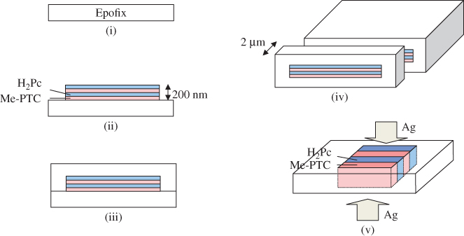
Figure 10 Fabrication process. (i) Substrate. (ii) Deposition. (iii) Embedding. (iv) Slicing. (v) Electrode deposition.
Reprinted with permission from Hiramoto [15]. Copyright© 2006 Wiley Periodicals, Inc.
When only the Me-PTC was selectively excited using monochromatic light of 480 nm wavelength under a relatively small applied electric field, the photocurrent generated in the vertical superlattice was reproducibly observed. Figure 11(a) shows the dependence of the photocurrent generation quantum efficiency on the layer width (x; Fig. 8(a)) of the vertical superlattice. The layer width (x) was varied down to 2.5 nm. A decrease in x means an increase in the number of interfaces between Me-PTC and H2Pc. At x = 2.5 nm, the number of layers will be 4 million layers per 1 cm. The quantum efficiency rapidly increases as x decreases, and the maximum, 41%, was observed at 10∼5 nm. However, it was also found that the efficiency decreased when the layer width decreased to 2.5 nm. Thus, we could experimentally determine the optimal width, x, at which the performance of photoelectric conversion in the Me-PTC/H2Pc system is maximized to be 10–5 nm.

Figure 11 (a) Dependence of photocurrent quantum efficiency on layer width (x). Only Me-PTC was excited by 480 nm monochromatic light in an electric field of 2 × 10⁴ V/cm. (b) Schematic illustration of the active area (shaded) in the vicinity of Me-PTC/H2Pc junction. The dead area (not shaded) in the Me-PTC layer decreases as the number of heterojunctions increases and is eliminated at x = 10 nm. (c) Semilogarithmic plot of the data in Fig. 11(a).
Reprinted with permission from Hiramoto [15]. Copyright© 2006 Wiley Periodicals, Inc.
The increase in the quantum efficiency by decreasing the layer width (x) is related to the exciton diffusion length. Photocurrent is generated when the photogenerated excitons dissociate into free electrons and holes when they reach the Me-PTC/H2Pc interface (Fig. 11(b)). The excitons that could not reach the boundary surface are deactivated. The range where the excitons can reach the interface is the active area in which the photocurrent is generated (shaded area), and the remainder where the excitons are deactivated is the dead area (nonshaded area). The increase in photocurrent quantum efficiency occurs due to an increase in the active area and a decrease in the dead area (Fig. 11(b)). In other words, when x is thick, that is, the number of interfaces is small, the majority region will be dead area, and only a small photocurrent is generated. When x becomes thin, that is, the number of interfaces increases, the photocurrent gradually increases due to the increase in the active area, and at x = 10–5 nm, the dead area in Me-PTC is eliminated and the maximum photocurrent is generated (Fig. 11(b)).
The exciton diffusion length can be obtained quantitatively. A semilogarithmic plot of the photocurrent quantum efficiency as a function of x (Fig. 11(c)) showed a clear linear relationship. This signifies that the concentration of the excitons that can contribute to the photocurrent decreases exponentially by increasing the distance from the interface. The distance at which 90% of the excitons can reach the interface in the case of Me-PTC was precisely determined to be 3.7 nm. Similarly, that for H2Pc was determined to be 5.0 nm by the selective excitation of H2Pc. As shown in Table I, by adopting the C60/H2Pc system, the exciton diffusion lengths for C60 and H2Pc were determined to be 1.7 and 4.6 nm, respectively.
Table I Distance for Which 90% of Excitons can Reach a D/A Heterointerface
| DA Combination | Me-PTC (nm) | H2Pc (nm) | C60 (nm) |
| Me-PTC/H2Pc | 4.4 | 5.0 | – |
| C60/H2Pc | – | 4.6 | 1.7 |
In Fig. 11(a), when the layer width became as narrow as x = 2.5 nm, the quantum efficiency decreased. When the film is less than 2.5 nm thick, each layer is not completely formed as a single sheet, and the probability of growth remaining as island regions becomes higher. Such spatial incompleteness of the extraction route decreases the efficiency of transporting the electrons and holes without recombination over a distance of 2 µm to each electrode.
The result of this study shows that eliminating any dead areas, which do not generate photocurrent, as well as ensuring the formation of a continuous route to transport the spatially separated electrons and holes, is critically important to obtaining high photocurrent generation quantum efficiency in photoelectric conversion using organic semiconductors.
B. Phase Separation
In this section, we describe a fabrication method for pseudo-vertical superlattices similar to Fig. 8(a) by using co-evaporant third molecules that act as a solvent during vacuum deposition [16]. By introducing co-evaporant third molecules onto a substrate heated to +80 °C during film growth, phase-separated and crystallized co-deposited films that improve carrier transport can be fabricated (Fig. 8(b)). The third molecules collide with the C60 and H2Pc and decrease the density of crystalline nucleation sites on the surface and promote the crystallization/phase separation process. The third molecules are not left in the co-deposited films at elevated substrate temperatures.
Figure 8(c) and (d) shows cross-sectional SEM images of a C60:H2Pc co-deposited film. Without the third molecules, an amorphous smooth cross-section was observed for the molecular-level mixture of C60 and H2Pc (Fig. 8(c)). On the other hand, with the third molecules, a columnar structure of phase-separated and crystallized material (Fig. 8(d)) similar to the ideal vertical superlattice (Fig. 8(a)) was formed. The improved crystallinity produced by introducing the third molecules was confirmed by UV–vis absorption spectra and X-ray diffraction analyses. Photocurrent enhancement was observed, particularly for relatively thick (>400 nm) co-deposited films having greater light absorption (see Section IV.B). A striking enhancement in photocurrent generation is achieved in organic solar cells without exception, based on a variety of co-deposited films such as H2Pc:C60, PbPc:C60, AlClPc:C60, and rubrene:C60. More than 10 kinds of low vapor pressure liquids such as polydimethylsiloxane (PDMS) and alkyldiphenylether (ADE) can be used as third molecules. Since ADE is a typical diffusion pump oil, the present effects can often be observed for co-deposition using a chamber evacuated by a diffusion pump (see Section IV.B). We believe that this method is generally applicable for growing high-quality phase-separated/crystalline co-deposited films for vacuum-deposited small-molecular-type organic solar cells.
There are reports of the successful construction of such vertical superlattices. A pseudo-vertical superlattice structure was fabricated by combining a new type of C60 derivative (SIMEF, Fig. 3) with benzoporphyrin (BP, Fig. 3) [14]. BP is formed by thermal conversion from a precursor. Since fabrication by wet processing was adopted, the phase separation occurred in the presence of a solvent. After removal of the C60 derivative (SIMEF) by washing in toluene, the desired interdigitated structure was clearly visible (Fig. 8(e)). The round columns of crystalline BP with diameters of around 20 nm stand almost vertically. This structure allows excitons to dissociate within their diffusion length and ostensibly inhibits the recombination of photogenerated electrons and holes. In 2013, Mitsubishi Chemical Co. Ltd succeeded in obtaining a power-conversion efficiency of 12% with this system. A commercial version using this system is illustrated in Fig. 2(a) and (b), which show a flexible see-through organic solar cell module and a demonstration building using these modules as exterior walls and windows [17]. This is a clear demonstration of the ideal vertical structure (Fig. 8(a)) showing practical conversion efficiency.
V. Energetic Structure Design
pn-Control by doping is indispensable for the solid-state physics of inorganic semiconductors. In the case of organic semiconductors, their genuine potential has been concealed for a long time by contamination with unintentional and unknown impurities, typically by oxygen from air. However, the author has a strong conviction that organic semiconductors should also be able to be treated in a similar way to inorganic semiconductors. Simultaneously, the author strongly expects that unknown physical phenomena peculiar to organic semiconductors will be discovered during the course of research to establish the solid-state physics of organic semiconductors.
We believe that the following points are indispensable for the complete pn-control of organic semiconductors. (i) a ppm-level doping technique should be applied to sub-ppm purified organic semiconductors. (ii) Complete pn-control, that is, the observation that every single organic semiconductor shows both n- and p-type characteristics by impurity doping alone, should be proven. (iii) Uncontrolled doping by oxygen and water from the air should be completely avoided to obtain reproducible results. (iv) For organic solar cell applications, the doping technique should be applicable not only to single organic semiconductor films but also to co-deposited films that have D/A sensitization capability (Section II.B).
In the following sections, we summarize “seven-nines”(3.7N) purification, pn-control of single and co-deposited organic semiconductors by doping, doping sensitization, and ppm-doping effects.
A. Seven-Nines Purification
1. Single-Crystal Sublimation
First, we focused on the high purification of organic semiconductors. Conventional p–i–n cells (Section II.D) [7, 8] incorporating a quasi-vertical superlattice (Section III.B) [16] were used to evaluate the effects of high purification.
Based on an analogy with inorganic Si, which is usually purified to eleven-nines (11N), the purity of organic semiconductors needs to at least reach the sub-ppm level in order to draw out their essential nature. Based on the aforementioned consideration, a more rigorous purification method was applied to organic semiconductors. Conventionally, organic semiconductors are purified by the “train sublimation” method under vacuum [18] and the purified samples are obtained as a powder. Alternatively, when the sublimation is performed at 1 atm, the purified samples are obtained as single crystals that are of extremely high purity due to gas convection [19].
Figure 12 shows a photograph of C60 (i), C70 (ii), H2Pc (iii), 6T (iv) crystals purified by single-crystal sublimation [19]. Crystal growth was performed in a quartz tube surrounded by a three-zone furnace system (Epitech Co., Ltd) under flowing N2 at 1 atm. For the case of C60, the C60 sample was set at 720 °C, and single crystals with sizes exceeding 2 mm × 2 mm were grown at around 500 °C. X-ray diffraction of the obtained crystals showed precise agreement with the reported crystal structure of C60. The obtained C60 crystals were used in the next single-crystal sublimation process.
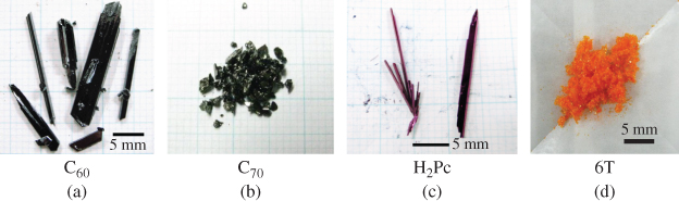
Figure 12 Photograph of single crystals of (a) C60, (b) C70, (c) H2Pc, and (d) 6T.
2. One-Micrometer-Thick Co-deposition Cells
Highly purified organic semiconductors produced by single-crystal sublimation were incorporated in p–i–n cells (Fig. 7(a)) (Section III.D, Fig. 13(a)). A p-type H2Pc layer (20 nm), a co-deposited C60:H2Pc i-interlayer, and an n-type layer of naphthalene tetracarboxylic anhydride (NTCDA) were successively deposited by vacuum evaporation at 1 × 10⁻³ Pa using a diffusion pump (VPC-260, ULVAC) onto an indium tin oxide (ITO) glass substrate pretreated in an air plasma. The thick NTCDA layer (600 nm) also acts as a transparent protection layer that prevents electrical shorting of the cells due to metal migration into the organic film during metal deposition [20, 21]. The co-deposition was performed on a substrate heated to +80 °C. The optimized C60:H2Pc ratio was 1.13:1. ADE, which acted as a co-evaporant third molecule (Section VI.B), was automatically introduced from the diffusion pump. A phase-separated/crystalline nanostructure (Fig. 8(d)) was confirmed to be formed for the present C60:H2Pc co-deposited film.

Figure 13 (a) Structure of organic p–i–n solar cell. The C60:H2Pc co-deposited layer (thickness: X nm) having a quasi-vertical superlattice structure (Fig. 8(a,d)) sandwiched between p-type H2Pc and n-type NTCDA. (b) Current–voltage (J–V) characteristics for a p–i–n cell with an i-layer thickness (X) of 250, 600, 960 nm, and 1.2 µm. Cell parameters (X = 960 nm); Jsc: 18.3 mA/cm2, Voc: 0.40 V, FF: 0.53, efficiency: 5.3%. The simulated light intensity transmitted through the ITO glass substrate is 74.2 mW/cm2.
Figure 13(b) shows the current–voltage (J–V) characteristics of the cells in Fig. 13(a) with co-deposited layer thicknesses, X, of 250, 600, 960 nm, and 1.2 µm, incorporating a C60 sample purified three times by single-crystal sublimation. Figure 14 shows the dependence of the fill-factor (FF) and the short-circuit photocurrent density (Jsc) on X. Surprisingly, FF hardly decreases even for an extremely thick i-co-deposited layer of 1.2 µm (open circles). Simultaneously, Jsc increases with X and reaches a maximum value of 19.1 mA/cm2. On the contrary, when the C60 is purified by conventional train sublimation under vacuum, FF monotonically decreases with co-deposited layer thickness (Fig. 14(a), open squares) [22]. At X = 960 nm, a Jsc value of 18.3 mA/cm2 and a conversion efficiency of 5.3% were observed [23, 24].1 The internal quantum efficiency reaches around 90% in the region from 400 to 700 nm for the X = 960 nm cell (Fig. 15(a)).
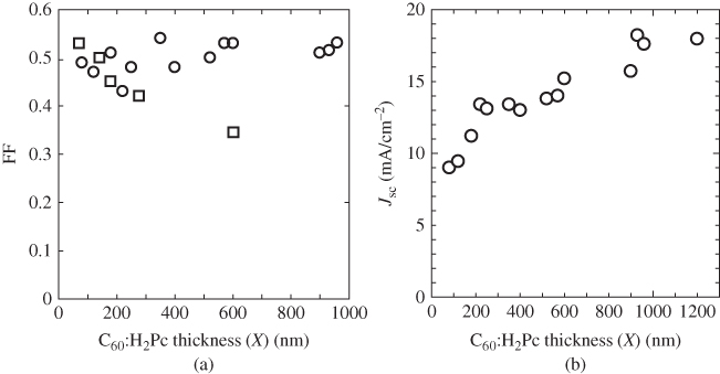
Figure 14 (a) Dependence of fill-factor (FF) on the C60:H2Pc i-interlayer thickness (X) for p–i–n cells incorporating C60 purified three times by single-crystal formed sublimation (open circles) and for those incorporating C60 purified by conventional train sublimation under vacuum (open squares). (b) Dependence of short-circuit photocurrent density (Jsc) on X.

Figure 15 (a) Spectral dependence of the internal quantum efficiency for a cell with X = 960 nm. (b) Spectral dependences of the light absorption ratio of cells with X = 180 nm (curve A), 600 nm (curve B), and 960 nm (curve C). (c) Photograph of cells with X = 180 nm (left) and 960 nm (right).
Figure 15(b) shows the spectral dependence of the absorption ratio of the cells. For a thin C60:H2Pc layer (X = 180 nm, curve A), a large portion of the visible light, especially around 500 nm, cannot be absorbed due to the low absorbance of C60. For an extremely thick C60:H2Pc layer (X = 960 nm, curve C), 95% of the visible light from 300 to 800 nm is absorbed. Figure 15(c) shows photographs of the cells with X = 180 nm (left) and 960 nm (right). For X = 180 nm, the cell color is a transparent green, that is, a large portion of the visible light is not absorbed and therefore cannot be utilized. For X = 960 nm, the cell color is an opaque dark brown, that is, almost all of the visible light is absorbed. The most important feature of the present cells is the incorporation of an extremely thick (1 µm) C60:H2Pc co-deposited layer into the cell without decreasing FF. This allows the utilization of the entire visible region of solar light.
To evaluate the purity of the C60 crystals at the ppm level, secondary ion mass spectroscopy with a Cs+ ion source (SIMS, ULVAC-PHI, 6650M) was used. Figure 16 shows the negative ion mass spectrum (i) and the depth profile (ii). Most of the peaks are assigned to carbon (C1, C2, etc. and their isotopes). As impurities, only oxygen (O) and hydrogen (H) were detected. The intensity of 101 in the depth profile corresponds to the detection limit for the elements. For O atoms, the detection limit corresponds to a concentration of about 8 × 10¹⁵ atoms/cm3 [25]. Taking this value into account, we conclude that the purity of the C60 has reached at least seven-nines (99.99999%, 7N). A purity of 7N was also confirmed by temperature-programmed desorption mass spectroscopy. The main impurity is revealed to be oxygen. C60 molecules interacting with oxygen seem to be the main impurities. Oxidized C60 (C60Ox) has been reported to act as an electron trap [26]. It is probable that the absence of C60Ox traps greatly enhances the electron diffusion length (L = (Dτ)1/2; D: diffusion coefficient, τ: electron lifetime) by increasing the lifetime (τ).
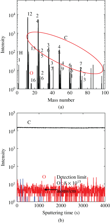
Figure 16 Negative ion mass spectrum (a) and depth profile (b) of SIMS measurements for C60 crystal purified three times by single-crystal sublimation.
The overall results in this section suggest that both high purification and phase separation are necessary to fabricate 1-µm-thick C60:H2Pc co-deposited cells.
B. pn-Control by Doping
1. Background
Organic semiconductors have been recognized as being affected by unintentional contamination from impurities that act as donors, acceptors, traps, and so on. Uncontrolled impurities due to incomplete purification and due to contamination from air masked the real nature of organic semiconductors for a long time. A typical example is oxygen. Since oxygen from air, which acts as an acceptor impurity, is doped in many kinds of organic semiconductors such as phthalocyanines, they always show p-type character. The prevention of exposure to oxygen by the use of ultra-high vacuum during film deposition and subsequent measurements has revealed that phthalocyanines are fundamentally n-type in nature [27, 28]. A few exceptional kinds of organic semiconductors, such as perylene pigments (e.g., Im-PTC and Me-PTC (Fig. 3)) that are not affected by oxygen even in air show n-type character.
Though impurity doping into organic semiconductors has already been studied, the types of dopants used were very limited. As acceptor dopants, halogen vapors such as I2 or Br2 were used [29, 30]. After Br2 doping, perylene pigment changed its conduction type from n- to p-type, and pn-homojunctions could be formed [31]. On the other hand, as donor dopants, there were few choices except alkaline metals such as Na and Ca, which are easily oxidized in air.
In the last decade, however, due to spin-offs from organic EL technology, several new kinds of dopants have been identified, initially for the carrier injection layers. As acceptors, organic dopants such as F4-TCNQ [32, 33] and F36C60 [34] and inorganic dopants such as MoO3 and V2O5 [35, 36] were identified. In terms of donors that are relatively stable in air, Harada et al. found a Ru complex and applied it to fabricate pn-homojunctions in zinc phthalocyanine [37, 38] and pentacene [39]. Recently, compounds of alkaline metals such as Cs2CO3 [40, 41] and Co complexes [42] that act as donor dopants have been identified. Progress in the search for dopants for organic semiconductors is summarized in Ref. [43].
2. Method of ppm-Level Doping
Organic semiconductor samples of at least 7N purity were used (Fig. 12). MoO3 (Alfa Aesar, 99.9995%) and V2O5 (Aldrich, 99.99%), and Cs2CO3 (Aldrich, 99.995%) were used as dopants for acceptors and donors, respectively (Fig. 17(a)).

Figure 17 (a) “Three-sources” co-deposition. MoO3 and V2O5, acting as acceptors, and Cs2CO3 acting as a donor were doped in the H2Pc:C60 (1:1) co-deposited film. (b) An example of the total thickness signal from QCM versus time relationship for 9 ppm doping. (c) Rotating slit having an aperture ratio of 1/10.
Multiple component co-evaporation techniques were employed to simultaneously evaporate organic semiconductors and dopants. In the case of doping into single organic semiconductor films, a two-component co-evaporation technique was employed. In the case of doping into C60:H2Pc and C60:6T co-deposited films, a three-component co-evaporation technique (Fig. 17(a)) was employed. An oil-free vacuum evaporator (Epitech Inc., ET300-6E-HK) was used for co-evaporation on ITO glass substrates at a chamber pressure of 10−5 Pa.
Precise monitoring of the deposition rate using a QCM equipped with a computer monitoring system (ULVAC, CRTM-6000G/Depoview) allowed us to introduce the dopants down to a very low concentration of 9 ppm by volume [44]. Figure 17(b) shows an example of the total thickness signal for the QCM versus time relationship as monitored by a PC display for 50 ppm MoO3 doping. There was a very slow cyclical fluctuation in the material due to temperature fluctuations in the cooling water for the QCM caused by on/off cycling of the chiller. However, a reproducible increase in the baseline (dark grey line), which was only observed during MoO3 evaporation for a prolonged timescale of 3500 s was observed (1.8 × 10⁻⁶ nm/s). The evaporation rate of the organic semiconductors was maintained at 0.2 nm/s. Therefore, a doping concentration of 9 ppm by volume can be obtained (1.8 × 10⁻⁶/0.2 = 9 × 10⁻⁶). Doping concentrations of 1 ppm were realized by reducing the dopant evaporation rate using rotating disks having slits with aperture ratios of 1/10 (Fig. 17(c)).
The Fermi level (EF) of the 100-nm-thick organic semiconductor films was measured using a Kelvin vibrating capacitor apparatus (Riken-Keiki, FAC-1). Both the evaporation chamber and the Kelvin probe were built into a glove box (Miwa, DBO-1.5) purged with N2 gas (O2 < 0.2 ppm, H2O < 0.5 ppm). During the film deposition and the EF and photovoltaic measurements, none of the organic films were exposed to air at any time. Removal of the influence of O2 is indispensable for obtaining accurate EF measurements of organic semiconductor films. The EF values were easily perturbed if the organic films were exposed to air even once, especially by the ingress of O2 into the films, and then reproducible results could not really be obtained.
3. pn-Control of Single C60 Films
In Fig. 18, energy diagrams of the C60 (left side) and MoO3 (right side) films are shown. The MoO3 showed a remarkably positive value of EF at 6.69 eV, which is more positive than the upper edge of the valence band (VB) of C60 (6.4 eV), as determined by X-ray photoelectron spectroscopy [45, 46]. The value of EF for nondoped C60 (middle line) is located at 4.6 eV, near the lower edge of the conduction band (CB), suggesting that this film is n-type in nature. When MoO3 was doped at a concentration of 3000 ppm, the value of EF shifted toward the positive direction and reached 5.88 eV, which is close to the upper edge of the VB (6.4 eV). This result strongly suggests that MoO3-doped C60 is p-type.
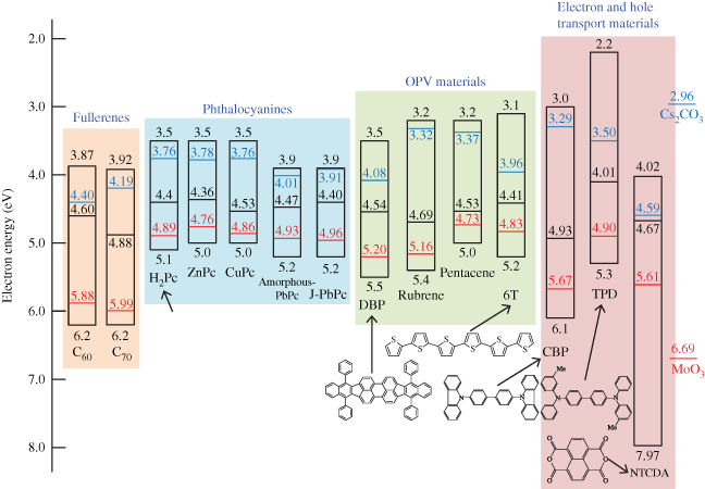
Figure 18 Energy diagrams of various organic semiconductor films. The middle, lower, and upper located lines show the energetic position of EF for nondoped, MoO3-doped, and Cs2CO3-doped films. The doping concentration is 3000 ppm. EF for the MoO3 and Cs2CO3 films (100 nm) are also shown.
To investigate the kinds of interactions that occur between C60 and MoO3, the absorption spectra of a co-deposited film with a ratio of 1:1 were obtained. Though single films of MoO3 and C60 are transparent and weak-yellowish transparent, respectively, a new strong absorption from 500 to 1800 nm appeared for the co-deposited MoO3:C60 (1:1) film and the film color changed to black (Fig. 19(a), upper photograph). This new absorption can be attributed to CT absorption between C60 and MoO3. Absorption spectrum of the CT band appeared in Ref. [47]. Based on the energy diagram (Fig. 18), it is reasonable to infer that MoO3 extracts electrons from the VB of C60. The middle figure in Fig. 19(a) shows the mechanism of p-type C60 formation. A CT complex, that is, C60+–MoO3−, is formed. Here, the negative charge on the MoO3− group can be regarded as a spatially fixed ion, that is, an ionized acceptor. On the other hand, the positive charge on C60+ can be liberated from the negative charge on the MoO3− by heat energy at room temperature and can migrate into the C60 film and act as a free hole in the VB of C60. This increase in hole concentration causes the large positive shift of EF that is observed (Fig. 18). This is a process similar to the formation of free holes in p-type silicon (Fig. 19(a), lower). V2O5 was also confirmed to act as an acceptor in C60.
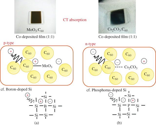
Figure 19 (Upper) Photographs of C60:MoO3 (1:1) film (a) and C60:Cs2CO3 (10:1) film (b). Strong CT absorption was observed. (Middle) Mechanisms of p- and n-type C60 formation by MoO3 (a) and Cs2CO3 (b) doping. (Lower) Corresponding mechanisms of p- and n-type Si formation by B (a) and P (b) doping.
For the 3000 ppm Cs2CO3-doped C60 film, the value of EF shifted negatively to 4.40 eV, which is close to the lower edge of the CB of C60 (4.0 eV) [45]. A thick co-deposited film of C60:Cs2CO3 in the ratio 10:1 changed color to dark grey (Fig. 19(b), upper photograph), that is, it showed a new broad CT absorption. Since the work function of Cs2CO3 (2.96 eV) is more negative than the CB of C60 (4.0 eV), it is reasonable that Cs2CO3 donates an electron to C60 and forms a CT complex, that is, C60−–Cs2CO3+. The formation of n-C60 by Cs2CO3 doping is caused by the opposite mechanism to MoO3 doping (Fig. 19). The donor ability of Cs2CO3 did not disappear even after exposure to air.
4. pn-Homojunction Formation in Single C60 Films
Since both p- and n-type C60 were formed, we tried to fabricate pn-homojunctions in single C60 films [48, 49]. Three types of cells with different thickness combinations of p- and n-doped layers, that is, 250/750 nm (a), 500/500 nm (b), and 750/250 nm (c) were fabricated (Fig. 20). The total thickness of the C60 was maintained at 1 µm for all cells. Figure 21 shows the action spectra for the three types of cells. Under irradiation onto the ITO electrode (Fig. 20(a), hν(ITO)) and with the homojunction located at the ITO side (Figs. 3.20(a) and 3.21(a, curve A)), photocurrent mainly appeared between 400 and 500 nm, which corresponds to the visible absorption region of the C60 film (black curve). For the homojunction at the center of the cell (Figs. 3.20(b) and 3.21(a, curve B)), the photocurrent decreased and shifted to longer wavelength and the main peak was located at the edge of the C60 absorption. Finally, for the homojunction on the Ag side (Figs. 3.20(c) and 3.21(a, curve C)), the low magnitude photocurrent shifted to a wavelength far longer than 500 nm, where there is little C60 absorption. The observed systematic change in the shape of the action spectra with respect to the distance of the homojunction from the light-irradiated electrode can be attributed to the so-called “masking effect.” This means that photocarrier generation occurs mainly in the neighboring regions of the p/n-doped interface (active zone) and that, by retracting this homojunction from the light-irradiated ITO surface, a dead layer is gradually grown in front of this active zone.

Figure 20 Three structures of pn-homojunction C60 cells. The thickness combinations of the MoO3- and Ca-doped layers are 250/750 nm (a), 500/500 nm (b), and 750/250 nm (c). The concentration was kept at 5000 ppm for both dopants. hν(ITO) and hν(Ag) denote light irradiation onto ITO and onto Ag electrodes, respectively. The locations of the homojunctions are indicated by the arrows.
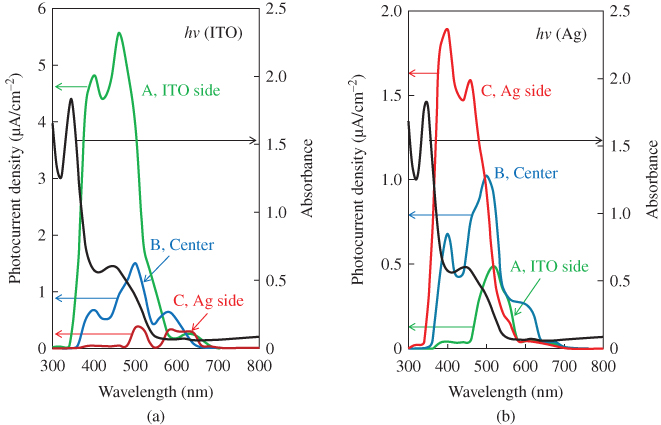
Figure 21 Action spectra under irradiation onto the ITO electrode (a) (hν(ITO)) and onto the Ag electrode (b) (hν(Ag)). Curves A, B, and C are for the cells (a), (b), and (c) in Fig. 20, respectively. The black curve shows the absorption spectrum of the C60 film (150 nm).
Under light irradiation onto the Ag electrode (Fig. 20, hν(Ag)), the homojunction approaches the illuminated electrode in the order of cells (a), (b), and (c). In this case, completely the reverse tendency, namely, an increase in the magnitude of the photocurrent and a shift toward shorter wavelength of the action spectra, were observed (Fig. 21(b), curves C, B, and A). This means that the dead layer between the active zone and the illuminated Ag electrode gradually disappeared. Apparently, the photoactive zone moves together with the homojunction. Even if the Ca donors were substituted with Cs2CO3 donors, fundamentally the same result was obtained. Since the width of the depletion layer pn-homojunction at the present doping concentrations of 5000 ppm MoO3/5000 ppm Cs2CO3 is calculated to be only 29 nm, which is far smaller than the total cell thickness of 1 µm, a strong masking effect (Fig. 21) was observed.
In Fig. 22, the energy structure of a pn-homojunction (doping concentration: 3000 ppm MoO3/500 ppm Cs2CO3) as measured by Kelvin band-mapping (see Section IV.D) is shown. Since there is a significant difference in EF, a built-in potential can be created by contacting the MoO3- and the Cs2CO3-doped C60 films (Fig. 18, left side). As a result, a pn-homojunction is formed. The observed direction of the photovoltage, whereby ITO/MoO3 is positive and BCP/Ag is negative, is consistent with this energy structure. The present results clearly show that pn-homojunctions were fabricated in the single C60 films by doping alone. In other words, the photovoltaic properties of organic semiconductor films could be intentionally designed by doping. We also confirmed the formation of pn-homojunctions for metal-free phthalocyanine (H2Pc) [50].
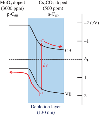
Figure 22 Energetic structure of pn-homojunction formed after contact measured by Kelvin band-mapping. The doping concentrations of Cs2CO3 and MoO3 are 500 ppm and 3000 ppm, respectively.
5. Generality
As shown in Fig. 18, other than fullerenes (C60 and C70), complete pn-control was accomplished for various phthalocyanines (H2Pc, ZnPc CuPc, PbPc), other photovoltaic organic semiconductors (rubrene, sexithiophene (6T), pentacene, DBP), and hole transport materials (CBP). In exceptional cases, due to the energy relationship, only p- and n-type control could be accomplished for TPD and electron transport material (NTCDA), respectively. These results strongly suggest that, in principle, almost all single organic semiconductors can be controlled to both n- and p-type by doping alone, similar to the case of inorganic semiconductors. For the cases of C60, H2Pc, ZnPc, pentacene, and CBP, pn-homojunctions were formed [36, 38, 40, 48, 50].
6. Band-Mapping by Kelvin Probe
The concentrations of carriers created by doping can be evaluated by using the Kelvin vibrating capacitor method [44, 51, 52]. Figure 23 shows the principle of band-mapping by Kelvin probe. When p-doped organic semiconductors are in contact with ITO electrodes, the EF values are aligned. Accordingly, the vacuum level (EVAC) is bent upward and the value of the work function, which is defined as the difference between EVAC and EF (double arrows), changes with the thickness of the films. Thus, the band-bending can be directly mapped (Fig. 23, lower) by measuring the work function using a Kelvin probe for changing thicknesses of doped films (Fig. 23, middle). Since the band-bending gives the depletion layer width (Wdep) and the built-in potential (Vbi), the carrier concentration (N) can be obtained by using the following Eq. (3.2).

Figure 23 Principle of band-mapping by Kelvin probe. An interface between ITO and a p-type semiconductor film is shown. Work function values (middle figure) corresponding to the double arrows (lower figure) depending on the thickness of the organic semiconductor film were measured by Kelvin probe. Evac, EF, CB, and VB denote the vacuum level, the Fermi level, the conduction band, and the valence band, respectively.
Reprinted with permission from Shinmura et al., 2014 [53]. Copyright© 2014 The Japan Society of Applied Physics.
Here, ϵ, ϵ0, and e are the relative dielectric constant, the dielectric constant of a vacuum, and the elementary charge.
Figure 24 shows the dependences of the work functions of the doped C60 films on the film thicknesses. In the case of Cs2CO3 doping, the work function was shifted toward the negative direction and reached close to the lower edge of the CB (3.9 eV) (triangles). In the case of MoO3 doping, the work function was shifted toward the positive direction and reached near the upper edge of the VB (6.4 eV) (circles). For both dopants, as the doping concentration increased, the film thickness at which the shift in the work function finished became thinner, and the magnitude of the energy shift became larger. Namely, Wdep decreased and Vbi increased. These band-bendings can be fitted by quadratic curves (Fig. 24, solid lines) based on the Poisson equation, and the values of Wdep and Vbi can be precisely determined. For example, in the cases of the n- and p-type band-bending of C60 films doped with Cs2CO3 (500 ppm) and with MoO3 (5000 ppm), electron and hole concentrations of 2.5 × 1017 cm−3 and 9.6 × 1017 cm−3 2 were obtained, respectively, from Wdep values of 24 and 21 nm and Vbi values of 0.29 and 0.87 V using a ϵ value of 4.4 for C60 [54].
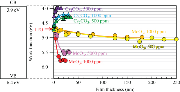
Figure 24 Work function shifts in C60 films doped with Cs2CO3 and MoO3 on ITO substrates (triangles and circles). Band-bending was fitted by a quadratic relationship based on the Poisson equation (solid curves).
Reprinted with permission from Shinmura et al., 2014 [53]. Copyright© 2014 The Japan Society of Applied Physics.
Figure 25(a) shows the dependence of carrier concentration on the doping concentration. When the Cs2CO3 doping concentration increased, the electron concentration rapidly increased and reached 1019 cm−3 at a doping concentration of 10,000 ppm. On the other hand, when MoO3 was used as the dopant, the carrier concentration showed a minimum value, that is, 4.3 × 1015 cm−3 at 500 ppm, and the hole concentration increased and reached 2.7 × 1018 cm−3 at 10,000 ppm. The minimum carrier concentration at 500 ppm with MoO3 doping suggests that the holes created by MoO3 doping compensate the inherent n-type nature of C60.

Figure 25 Dependence of carrier concentration (a) and doping efficiency (b) on doping concentration of Cs2CO3 or MoO3.
Reprinted with permission from Shinmura et al., 2014 [53]. Copyright© 2014 The Japan Society of Applied Physics.
Figure 25(b) shows the doping efficiency, which is defined as the ratio of the induced carrier concentration to the doped molecular concentration. The doping efficiencies of Cs2CO3 and MoO3 doping are about 10% and 3%, respectively. The doping process can be explained by the formation of a CT complex and its subsequent ionization (Fig. 19(middle) and Fig. 26(b)). So, the doping efficiency is expressed by the product of the rates of CT complex formation and ionization. In the case of Cs2CO3, since Cs2CO3 is a substantial molecule, by assuming that Cs2CO3 evaporates molecularly and the rate of CT complex formation with C60 is close to unity,3 the observed doping efficiency of 10% can be regarded as the ionization efficiency, which is significantly smaller than the value of 100% obtained for the donor dopant P in Si at room temperature. The orbitals of the electrons around the positive charge on the ionized donor in the cases of P doping in Si (a) and of Cs2CO3 doping in C60 (b) are shown in Fig. 26. Based on the fact that the ϵ value of Si is 11.9, the radius of the orbital of the electron around the positive charge of an ionized donor (P+) is calculated to be 3.3 nm. This situation is fundamentally similar to the Wannier exciton (Fig. 4(a)), and the electron is easily liberated from the positive charge by thermal energy at room temperature, and thus the ionization efficiency reaches unity (Fig. 26(a)). The only difference to the exciton is that the positive charge is spatially fixed in the crystal lattice.4 In the case of Cs2CO3 doping in C60, since the ϵ value of C60 is 4.4, the electron experiences a stronger attractive force from the positive charge. The radius of the Frenkel exciton is only 0.5 nm for C60 (Fig. 4(b)). However, a CT complex is formed by employing Cs2CO3 doping, that is, [Cs2CO3+–C60−] and the charges are separated on the neighboring molecules (Fig. 26(b)). This situation is fundamentally the same as the CT exciton (Fig. 5(b)) and the negative charge on C60 can be liberated by thermal energy at room temperature. Thus, significant values for the ionization efficiencies of electrons of about 10% were observed, though they were lower than the case of Si.
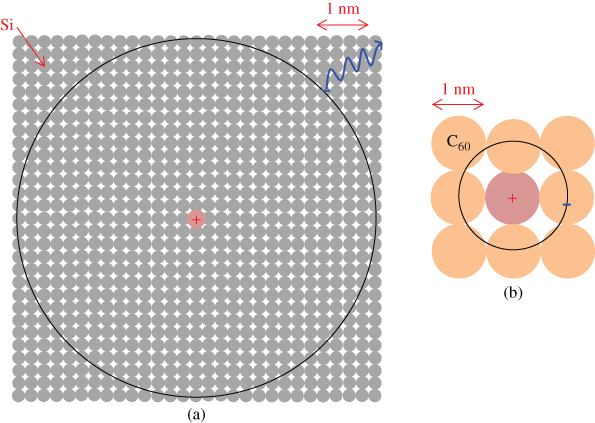
Figure 26 Orbital of electron around positive charge on ionized donor. (a) P doping in Si. P+ is represented by the dark grey shaded circle. This situation resembles the Wannier exciton (Fig. 4(a)). (b) Cs2CO3 doping in C60. Cs2CO3+ is represented by the dark grey shaded circle. This situation resembles the CT exciton (Fig. 5(b)).
Reprinted with permission from Shinmura et al., 2014 [53]. Copyright© 2014 The Japan Society of Applied Physics.
In the case of MoO3, a doping efficiency of 3% was obtained under the assumption that MoO3 forms the trimer (Mo3O9) [55]. Though a similar mechanism to that in Fig. 26(b) can also be applied in this case, in addition, the formation of larger MoOx clusters lowers the efficiency of CT complex formation, which seems to lower the total doping efficiency.
7. Organic/Metal Ohmic Junction
It is very important to make the two organic/metal contacts in a photovoltaic cell ohmic. When the region in the vicinity of a metal electrode is heavily doped, even if there is a Schottky barrier, its width becomes extremely thin allowing charge-carrier tunneling and, as a result, an ohmic contact is expected to be formed similar to that on heavily p+- or n+-doped inorganic semiconductors [43, 56, 57]. Here, + means heavily doped. Moreover, an ohmic contact can be formed irrespective of the electrode material used, since tunneling is less dependent on the metal work function, enabling the cell structure to be inverted. This technique would allow flexibility in the design of the cell structure.
As a test case, two-layer cells consisting of C60 and H2Pc (Fig. 27(a) and (b)) were examined [58]. The electrode materials were ITO and Ag. Heavy doping of the order of 10,000 ppm (1%) and 50,000 ppm (5%) were applied to thin 10 nm regions close to the C60 and H2Pc/metal interfaces. Figure 27(c) and (d) shows the current–voltage (J–V) characteristics for the cells with heavily doped regions in Fig. 27(a) and (b) (curves A). For the cell in Fig. 27(a), the FFreaches a value of 0.59 and clear rectification characteristics can be seen for the heavily doped regions (curves A). Without the heavily doped regions (curves B), however, FF is only 0.29, and the forward current is significantly suppressed. For the inverted cell (Fig. 27(b)), without heavily doped regions (Fig. 27(d), curves B), photovoltaic and rectification behavior are scarcely perceptible. However, with the heavily doped regions (curves A), the FF recovers, reaching a value of 0.49, and rectification is clearly observed. Clearly, the photovoltaic properties of the cells with thin heavily doped regions at the interfaces are independent of the type of electrode material used. Thus, H2Pc/C60 cells are invertible using this interfacial heavy-doping technique.

Figure 27 Structures of invertible two-layered H2Pc/C60 cells with heavily doped organic/metal interfaces. For the cells in (a) and (b), photogenerated holes and electrons are extracted to ITO and Ag, and to Ag and ITO, respectively. The total thicknesses of the H2Pc and C60 films are kept the same. (c) (d) Current–voltage (J–V) characteristics for cells (a) and (b) (curves A). The curves B are for the cells without heavily doped interfaces. The photocurrent and the dark current are shown by solid and broken curves, respectively. The ITO electrode was irradiated with simulated solar light (AM 1.5, 100 mW/cm2). Cell performances: (a) Jsc: 3.38 mA/cm2, Voc: 0.46 V, FF: 0.59, efficiency: 0.91%. (b) Jsc: 2.70 mA/cm2, Voc: 0.43 V, FF: 0.49, efficiency: 0.57%.
Kubo et al., 2012 [58]. Reproduced with permission of The Japan Society of Applied Physics.
Since electron extraction from C60 to the ITO electrode is crucial for the operation of the inverted cell (Fig. 27(d) (curves A)), we estimated the interfacial energy band structure of ITO/10,000 ppm Cs2CO3-doped C60 by Kelvin band-mapping (Fig. 28) (Section IV.B.6). There is a distinct barrier to electrons with a height of 0.34 eV from the CB of C60 to the ITO. However, since the band bends down steeply within 5 nm of the interface, photogenerated electrons can tunnel through this barrier. Heavily doped C60 acts as an n+-type semiconductor and makes the n+-C60/ITO junction ohmic. Organic/metal ohmic junctions can be fabricated by making tunneling contacts with heavy interfacial doping.

Figure 28 Energy structure for an ITO/n+-C60 contact measured by Kelvin band-mapping. A tunneling junction for photogenerated electrons is formed.
Kubo et al., 2012 [58]. Reproduced with permission of The Japan Society of Applied Physics.
C. pn-Control of D/A Co-deposited Films by Doping
1. pn-Control of Co-deposited Films
Co-deposited films consisting of D/A organic semiconductors are essential in order to generate photocurrent densities of significant magnitude based on the dissociation of excitons by the photoinduced electron transfer process (Figs 3.5(b)–(d), 3.7). So, for the application of this doping technique to organic photovoltaic cells, doping should be performed by regarding a co-deposited film consisting of two kinds of D/A organic semiconductors as a single semiconductor. We believe that the formation of a built-in potential by direct doping in the bulk of co-deposited films, where the generation and transport of photocarriers occurs, has the potential to enhance the efficiency of these cells [52]. Moreover, in these types of cells, a short exciton diffusion length is no longer a factor that limits cell performance.
Figure 29(a) shows the energy diagram for H2Pc:C60 co-deposited films. With donor (Cs2CO3) doping, EF has shifted from the undoped value of 4.48 eV (middle broken line) to 4.22 eV (upper broken line) and is close to the C60 conduction band (CBC60). Conversely, for acceptor (V2O5) doping, EF has shifted to 4.95 eV (lower broken line) and is close to the H2Pc VB (![]() ). Clearly, the conduction properties of the co-deposited films are controlled to both n- and p-type. It should be noted that the EF shift occurs within the band gap of co-deposited H2Pc and C60 films, that is, in between CBC60 and
). Clearly, the conduction properties of the co-deposited films are controlled to both n- and p-type. It should be noted that the EF shift occurs within the band gap of co-deposited H2Pc and C60 films, that is, in between CBC60 and ![]() . For n-type doping (Fig. 29(b)), free carriers (electrons) are produced in both H2Pc and C60, and they relax to the CB of C60. EF is fixed to 4.22 eV and is constant throughout the H2Pc and C60 (upper broken line). For p-type doping (Fig. 29(b)), holes are produced that relax to the top of the H2Pc VB. EF is fixed to 4.95 eV and is constant throughout the H2Pc and C60 (lower broken line). As a result, the shifts in EF are within the “bandgap of the co-deposited film.” Thus, control of the doping in the co-deposited film was accomplished [59, 60].
. For n-type doping (Fig. 29(b)), free carriers (electrons) are produced in both H2Pc and C60, and they relax to the CB of C60. EF is fixed to 4.22 eV and is constant throughout the H2Pc and C60 (upper broken line). For p-type doping (Fig. 29(b)), holes are produced that relax to the top of the H2Pc VB. EF is fixed to 4.95 eV and is constant throughout the H2Pc and C60 (lower broken line). As a result, the shifts in EF are within the “bandgap of the co-deposited film.” Thus, control of the doping in the co-deposited film was accomplished [59, 60].

Figure 29 pn-control of H2Pc:C60 co-deposited films by doping. EF shift occurs within the “bandgap of the co-deposited film.”
Kubo et al., 2013 [59]. Reproduced with permission of American Institute of Physics.
2. Organic/Organic Ohmic Junction
By making an n+p+ heavily doped double layer, organic/organic ohmic junctions can be fabricated [49, 61]. Figure 30(a) shows an n+p+-homojunction device fabricated in a C60:6T co-deposited film. MoO3 and Cs2CO3 were heavily doped (50,000 ppm (5%)) for the p+ and n+-regions, respectively. Obviously, the n+p+-homojunction showed good ohmic properties (Fig. 30(b)).
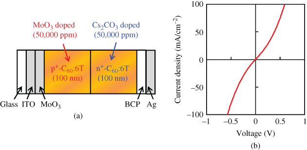
Figure 30 (a) Organic/organic ohmic n+p+-homojunction and (b) current–voltage characteristics.
3. Tandem Cells Formed by Doping
Tandem organic solar cells were first reported by the author in 1990 [62], and many types of cells that connect two unit cells have been fabricated [63]. The tandem organic solar cell, in which two single p+in+-homojunctions are connected by a heavily doped n+p+-ohmic interlayer, were formed in co-deposited films consisting of C60 and sexithiophene (6T) simply by doping [61]. Figure 31(a) and (b) shows the structures of a single p+in+-homojunction cell and a tandem cell connecting two p+in+-homojunctions formed in co-deposited C60:6T films. The following cell parameters were obtained: Jsc of 3.0 mA/cm2, Voc of 1.69 V, FF of 0.47, and a conversion efficiency of 2.4% (Fig. 31(c), curves B). Compared with the single cell (Fig. 31(c), curves A), Voc has doubled from 0.85 to 1.69 V. Obviously, the n+p+-homojunction in the tandem cell acts as an ohmic interlayer to connect the unit cells as shown in Fig. 30.

Figure 31 (a) Structure of a p+in+-homojunction cell fabricated in a C60:6T co-deposited film. Ishiyama et al., 2013 [61]. Reproduced with permission of Elsevier. A nondoped intrinsic C60:6T layer is sandwiched between heavily doped p+ and n+-C60:6T layers. (b) Structure of a tandem cell connecting two unit p+in+-homojunction cells by ohmic n+p+-homojunction. Ishiyama et al., 2013 [61]. Reproduced with permission of Elsevier. (c) Current–voltage (J–V) characteristics for a single p+in+-homojunction cell (curves A) and a tandem cell (curves B). The photocurrent and darkcurrent are shown by the solid and the broken curves, respectively. The ITO electrode was irradiated with simulated solar light (AM 1.5, 100 mW/cm2). The cell parameters, that is, Jsc, Voc, FF, and efficiency were as follows. Curve A: 4.5 mA/cm2, 0.85 V, 0.41, 1.6%. Curve B: 3.0 mA/cm2, 1.69 V, 0.47, 2.4%.
The overall energy band diagram of a tandem cell is shown in Fig. 32. In the case of the p+in+-homojunction cells formed in co-deposited C60:6T films, there are C60/6T heterointerfaces at which photoinduced electron transfer can occur throughout the entirety of the cells. Thus, under light irradiation, electrons and holes are photogenerated in both the front and back cells. Electrons and holes that move toward the n+p+-ohmic interlayer neutralize each other due to recombination or tunneling. This process is consistent with the observed photovoltaic properties of the present tandem cell (Fig. 31). It should be stressed that the present results proved that built-in potentials, such as homojunctions and tandem junctions, can be intentionally formed in bulk co-deposited films induced by doping alone. Methods for band-mapping in organic pn-homojunctions are explained in Section V.D.
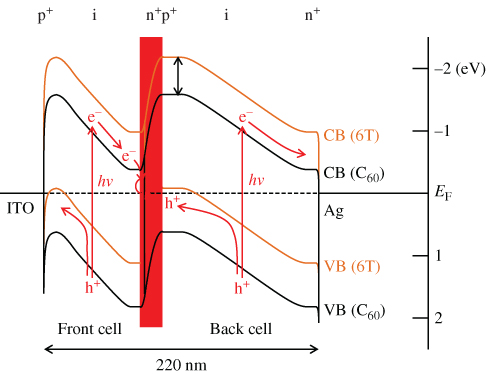
Figure 32 Energy band diagram of a tandem cell depicted based on Kelvin probe measurements. The shaded region corresponds to the depletion layer for an n+p+-homojunction acting as an ohmic interlayer. VB and CB denote the valence band and the conduction band, respectively. The bands for C60 and 6T are shown by the black and orange curves, respectively.
Ishiyama et al., 2013 [61]. Reproduced with permission of Elsevier.
D. Band-Mapping of Organic pn-Homojunctions
In this section, precise band-mapping in organic pn-homojunctions with various balances between the doping concentrations of the p- and n-type layers, that is, (i) a p+n+-homojunction in 6T:C60 (p+-layer doped with MoO3 at 50,000 ppm and n+-layer doped with Cs2CO3 at 50,000 ppm), (ii) a pn-homojunction in 6T:C60 (p-layer doped with MoO3 at 3000 ppm and n+-layer doped with Cs2CO3 at 500 ppm), and (iii) a pn+-homojunction in H2Pc:C60 (p-layer doped with V2O5 at 1000 ppm and n+-layer doped with Cs2CO3 at 10,000 ppm) was performed [64]. Here, “+” means heavily doped.
In order to obtain the potential profiles of the pn-homojunctions, the film thickness dependence of the work function in both p-type layers on n-type layers and vice versa were measured using a Kelvin probe. The shift in the work function on the p-side can be observed by repeated deposition and measurement of the work function of a p-type layer on a 100-nm-thick n-type layer. Similarly, the shift in the work function for the n-side can be observed by repeated deposition and measurement of the work function of an n-type layer on a 100-nm-thick p-type layer.

For the heavily doped p+n+-homojunction (i), the bulk values of EF in 100-nm-thick p+- and n+-layers were determined to be 5.58 and 4.38 eV, respectively. Variations in the work function (φ) with film thickness in the n+- and p+-type regions of the junction are shown in Fig. 33(a) and (b), respectively. On the n+-type side, φ becomes rapidly less positive as we move away from the interface, converging toward a value of 4.44 eV at a depth of about 3 nm, which is close to the value of EF for 100-nm-thick n+-6T:C60 (4.38 eV). This indicates that a space charge layer (SCL) is formed up to 3 nm into the n+-type region. On the other hand, on the p+-type side, φ becomes more positive as we move away from the interface, converging toward a value of 5.63 eV at a depth of about 15 nm, which is close to the value of EF for 100-nm-thick p+-6T:C60 (5.58 eV). Thus, the SCL is formed up to 15 nm into the p+-type region. Since the values toward which φ converge and the values of EF in the 100 nm films agree well, we conclude that, in thermal equilibrium, full alignment of the Fermi level between the p+- and n+-type films is realized. Thus, we can say that the depletion layer widths (Wn) for the n+-type region and (Wp) for the p+-type region are 3 and 15 nm, respectively, that is, the total depletion layer width (W) is 18 nm, and the built-in potential (Vbi), which is the difference between the bulk EF of n+-6T:C60 and that of p+-6T:C60, is 1.22 eV. Using these parameters, the ionized dopant concentrations for the n+- and p+-type regions, ND+ and NA–, respectively, can be estimated. According to the standard theory for uniformly doped inorganic semiconductors, the total depletion layer width (W) of a pn-junction is given by Eqs (3.3) and (3.4) [65].

Figure 33 Work functions in the p+n+-homojunctions. (a) n+ on p+. (b) p+ on n+. The black squares and solid curves are the observed points and the simulated curves, respectively. Wn, Wp, and Vbi denote the depletion layer widths in the n+- and p+-regions, and the built-in potential, respectively.
Yamashina et al., 2015 [64]. Reproduced with permission of American Institute of Physics.
Here, ϵr, ϵ0, q, xp, and xn denote the relative dielectric constant of the semiconductor, the dielectric permittivity in a vacuum, the elementary charge, and the depletion layer width in the p- and n-type regions, respectively. Furthermore, from Eq. (3.4), since xn = Wn = 3 nm and xp = Wp = 15 nm, we obtain the relationship ND+ = 5 NA–. Together with Vbi = 1.22 eV, we find from Eq. (3.3) that ND+ = 1.1 × 1019 cm−3 and NA– = 2.2 × 1018 cm−3.
The electric potential distribution in the p+n+-junction can be described by integrating Poisson's equation twice (3.5) and (3.6) with the values of Wn, Wp, ND+, and NA–, as shown in Fig. 34 (solid curve).


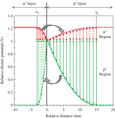
Figure 34 Electric potential profile (solid curve) in the p+n+-homojunction in Fig. 33 illustrated based on Poisson's equation. The point x = 0 corresponds to the p+n+ interface. The work function change in Fig. 33(a) (solid curve) is calculated by adding the potential change that occurred in n+-layer (left solid double-headed arrow) and that which occurred in p+-layer (left broken double-headed arrow). The work function change in Fig. 33(b) (solid curve) is calculated by adding the potential change that occurred in p+-layer (right solid double-headed arrow) and that which occurred in p+-layer (right broken double-headed arrow).
Yamashina et al., 2015 [64]. Reproduced with permission of American Institute of Physics.
Here, the left solid and right solid parts of the curve are the electric potentials in the n+- and p+-type regions, respectively.
Based on this distribution, we attempted to reproduce the observed work function change (Fig. 33, black squares). When an n+-type layer is deposited stepwise on the p+-type layer, an energy band is bent not only in the n+-type layer but also simultaneously in the underlying p+-type layer. Taking account of the fact that the total amounts of charge due to ionized dopants in the n+-region (ND+xn) and the p+-region (NA–xp) are identical, by depositing a xn-thick n+-layer on the p+-layer, band-bending up to a depth of xn in the n+-layer and up to a depth of xp in the underlying p+-layer develop simultaneously. So, in order to calculate the change in work function, the potential change that occurred in n+-layer (left solid double-headed arrow) and that which occurred in the p+-layer (left broken double-headed arrow) should be added together as shown in the n+-region in Fig. 34. Here, the light grey broken curve is obtained by inverting and shrinking in width the light grey solid curve from xp to xn. The calculated work function (Fig. 33(a), black solid curve) clearly reproduces the observed work function (Fig. 33(a), black squares).
Conversely, when a p+-type layer was deposited stepwise on the n+-type layer, the band is not only bent in the p+-type layer but also in the underlying n+-type layer. In order to calculate the change in work function, the potential change that occurred in the p+-layer (right solid double-headed arrow) and that which occurred in the n+-layer (right broken double-headed arrow) should be added together as shown in the p+-region in Fig. 34. Here, the dark grey broken curve is obtained by inverting and extending in width the dark grey solid curve from xn to xp. Again, the calculated work function (Fig. 33(b), black solid curve) clearly reproduces the observed work function (Fig. 33(b), black squares). Irrespective of whether the n+-layer is deposited on the p+-layer or the p+-layer is deposited on the n+-layer, the change in the work function can be reproduced by the calculation. This supports the validity of the values of Wp, NA–, Wn, and ND+ obtained and the potential distribution in Fig. 34 (solid curve).
The energy band diagram for the p+n+-homojunction can be illustrated precisely by turning the potential distribution shown in Fig. 34 (solid curve) upside down (Fig. 35). Since this p+n+-homojunction has an extremely narrow depletion layer width (W) of 18 nm, it confirms that it behaves as an organic/organic ohmic junction due to tunneling (see Sections IV.C.2 and IV.C.3).
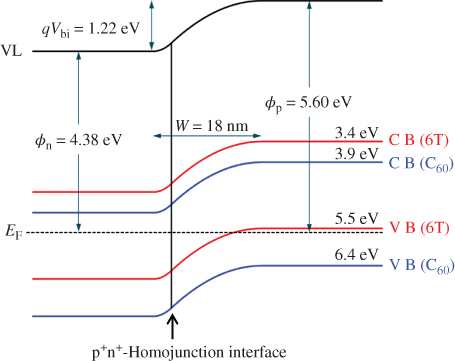
Figure 35 Energy band diagram of the p+n+-homojunction illustrated in Fig. 33 based on the solid curve in Fig. 34. VL, EF, VB, and CB denote the vacuum level, Fermi level, the valence band, and the conduction band, respectively. Φn and Φp are the bulk work functions of n+- and p+-6T:C60. The bands for 6T and C60 are shown by the light grey and dark grey lines, respectively.
Yamashina et al., 2015 [64]. Reproduced with permission of American Institute of Physics.
For lightly doped pn-homojunctions (ii), as in the case of the first sample, the simulated curve (Fig. 36, solid curves) reproduces the observed changes in the work function (Fig. 36, black squares), and the value of both Wn and Wp was 22 nm. As a result, ND+ and NA– were both determined to be 5.0 × 10¹⁷ (Fig. 36(a) and (b)). These values of ND+ and NA– almost accord with those obtained from band-bending measurements made in Schottky junctions, that is, ITO/n-6T:C60 (6.0 × 1017 cm−3) [66] or p-6T:C60 (3.0 × 1017 cm−3). The consistency between the parameters in the pn-homojunction and the corresponding Schottky junctions supports the validity of the obtained ionized dopant concentrations.

Figure 36 Work functions in the pn-homojunction. (a) n on p. (b) p on n. The black squares and solid curves are the observed points and simulated curves, respectively. (c) Energy band diagram of the pn-homojunction for panels (a) and (b).
Yamashina et al., 2015 [64]. Reproduced with permission of American Institute of Physics.
For the pn+-homojunction (iii), since the doping concentration of the n+-region is considerably greater than that of the p-region, it is assumed that in the case of an n+p-junction, which forms a one-sided abrupt junction, the SCL spreads predominantly into the p-region. As shown in Fig. 37(a) and (b), as expected, the band-bending mainly occurred in the p-region (Fig. 37(b)). On the other hand, a sharp decrease in the work function was observed to a depth of 2 nm in the n+-region. This means that the positive charge within 2 nm of the interface is sufficient to compensate for the negative charge in the depletion layer of the p-region. Conversely, deposition of an n+-layer of only 2 nm thickness on the p-layer can induce band-bending of 92 nm width in the underlying p-layer. The values of Wp and Wn that were obtained were 92 and 2 nm (see inset in Fig. 37(a)), respectively. As a result, ND+ and NA– were determined to be 1.9 × 10¹⁸ and 4.2 × 1016 cm−3, respectively (Fig. 37(a) and (b)). The values of ND+ and NA– accord with those obtained from band-bending measurements made on a Schottky junction, that is, ITO/p-H2Pc:C60 (4.3 × 1016 cm−3), which has a similar energy structure to an n+p-junction (Fig. 37(c)). Again, the simulated curves (Fig. 37(b), solid curves) precisely reproduce the observed changes in work function (Fig. 37(b), open squares).
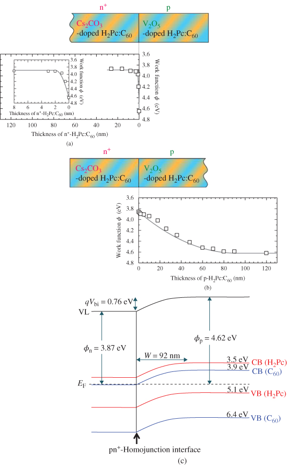
Figure 37 Work functions in the pn+-homojunctions. (a) n+ on p. (b) p on n+. Inset: Magnified view of the work function shifts within the first 8 nm for n+ on p. The open squares and solid curves are the observed points and simulated curves, respectively. (c) Energy band diagram of the pn+-homojunction for panels (a) and (b).
Yamashina et al., 2015 [64]. Reproduced with permission of American Institute of Physics.
The energy band diagram in the present n+p-homojunction based on the simulated curve is shown in Fig. 37(c). Since the ionized donor concentration is significantly greater than the ionized acceptor concentration, a one-sided abrupt junction, in which the SCL spreads predominantly into the p-type region, is formed.
We have demonstrated precise mapping of the band-bending in three cases, a p+n+-homojunction (i), a pn-homojunction (ii), and a pn+-homojunction (iii), irrespective of the doping concentrations of the n- and p-layers and the balance between the doping concentrations of these layers. It was revealed that the consideration of the change in band-bending in the underlying n-(or p-)type layer when a p-(or n-)type layer is gradually accumulated on it is necessary. The validity of the conventional theory for the SCL suggests that the dopants are spatially fixed even in organic semiconductor films. The present results clearly show that the precise configuration of the built-in electric field in organic photovoltaic cells is fundamentally identical to that in inorganic cells.
E. Doping Sensitization
Sensitization of the ionization for both n- and p-type doping in organic semiconductor co-deposited films was observed [53]. A significantly high ionization efficiency of 97%, comparable to that for silicon (100%), was achieved.
By making accurate estimations of the carrier concentrations generated by impurity doping by means of Kelvin band-mapping, we found evidence of higher doping efficiencies for co-deposited films compared with those for the respective single films. Thus, we tried to clarify the reasons for the difference between the doping efficiencies in co-deposited films and single films of organic semiconductors. As a typical case, we chose metal-free phthalocyanine: fullerene (H2Pc:C60, H2Pc:C70) and metal-free phthalocyanine:perylene pigment (H2Pc:Me-PTC) co-deposited films because of their high capability for exciton dissociation in organic solar cells. Cesium carbonate (Cs2CO3) and iron chloride (FeCl3) were used as donor and acceptor dopants, respectively. The deposition rate for the organic semiconductors was kept to 0.1 nm/s, and those for the dopants were adjusted from 10−5 to 2 × 10⁻³ nm/s to give doping concentrations from 0.0002 to 0.05 in molecular ratio (MR), that is, 50–10,000 ppm by volume.
Figure 38 shows an energy band diagram of the organic semiconductors and dopants used. Cs2CO3 can donate an electron to the CBs (LUMOs) of H2Pc (3.2 eV) and the fullerenes (3.9 eV) [67], which can be measured by near ultraviolet inverse photoemission spectroscopy [68], and thus acts as a donor since its work function is located at a shallower position (2.96 eV). In practice, by Cs2CO3 doping (MR = 0.02), the Fermi level (EF) shifted toward the positive direction and reached 3.97, 4.00, and 3.48 eV for C60, C70, and H2Pc, respectively. Both the fullerenes and the H2Pc became n-type. On the other hand, FeCl3 can withdraw an electron from the VBs (HOMOs) of H2Pc (5.1 eV) and Me-PTC (5.4 eV) and act as an acceptor since its work function is located at a deeper position (5.52 eV). By FeCl3 doping (MR = 0.03), EF shifted toward the negative direction and reached 4.72 and 5.04 eV for H2Pc and Me-PTC, respectively. Both H2Pc and Me-PTC became p-type.
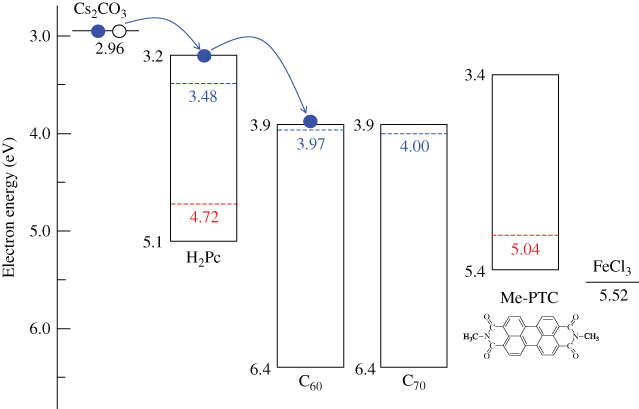
Figure 38 Energy diagrams of organic semiconductors. The work functions with donor (Cs2CO3) and acceptor (FeCl3) dopants are also shown. EFs of C60, C70, and H2Pc films doped with Cs2CO3 (MR = 0.02) are shown by upper broken lines. EFs of H2Pc and Me-PTC films doped with FeCl3 (MR = 0.03) are shown by lower broken lines.
Shinmura et al., 2014 [53]. Reproduced with permission of American Institute of Physics.
Figure 39(a) shows the film thickness dependence of the work function for Cs2CO3-doped H2Pc:C60 (1:1) co-deposited films (circles) and the respective Cs2CO3-doped single films of C60 (diamonds) and H2Pc (triangles). The shifts in work function due to the band-bending by doping are fitted by quadratic functions based on the Poisson equation (solid curves), which excludes the effect of a dipole layer of a few nanometers thickness in the vicinity of the ITO electrode [69]. Clearly, the depletion layer width (Wdep) in the H2Pc:C60 co-deposited film has shrunk to 10 nm from 20 to 30 nm in the respective C60 and H2Pc single films (arrows). This observation is a sign of an increase in the carrier concentration. Concentrations of 3.2 × 10¹⁸, 4.3 × 10¹⁷, and 4.6 × 1017 cm−3 were obtained for the co-deposited film and for the C60 and H2Pc films, respectively. By mixing C60 and H2Pc, the number of carriers created by Cs2CO3 doping was increased by a factor of around 10.

Figure 39 Film thickness dependences of the work function. (a) H2Pc:C60 (1:1) co-deposited film (circles) and its component single C60 (diamonds) and H2Pc (triangles) films. The Cs2CO3 doping concentration for all the films was MR = 0.005. (b) H2Pc:Me-PTC (1:1) co-deposited film (circles) and its component single Me-PTC (squares) and H2Pc (triangles) films. The FeCl3 doping concentration for all of the films was MR = 0.03. The depths of the band-bending are indicated by the arrows. The solid curves are quadratic fits to the band-bending.
Shinmura et al., 2014 [53]. Reproduced with permission of American Institute of Physics.
Essentially the same result was obtained for the H2Pc:Me-PTC (1:1) system (Fig. 39(b)). FeCl3 acting as an acceptor was introduced into a H2Pc:Me-PTC co-deposited film and its respective Me-PTC and H2Pc single films. Concentrations of 8.7 × 10¹⁸, 5.3 × 10¹⁶, and 6.9 × 1017 cm−3 were obtained for the co-deposited film and the Me-PTC and H2Pc films, respectively. By mixing Me-PTC and H2Pc, the number of carriers created by FeCl3 doping was also increased by a factor of about 100 for Me-PTC.
Figure 40 shows the dependence of the carrier concentration and the doping efficiency on the doping concentration for H2Pc:C60 (a,b) and H2Pc:C70 (c,d) co-deposited films and their component films. The doping efficiency is defined by the ratio of the carrier concentration created to the molecular concentration of Cs2CO3. Obviously, the carrier concentration is an order of magnitude higher for the co-deposited films (Fig. 40(a) and (c), curves A and D) compared with the respective component single films (Fig. 40(a) and (c), curves B, C, and E). The doping efficiencies of single films of C60, C70, and H2Pc are around 10% (Fig. 40(b) and (d), diamonds and triangles). In contrast, the doping efficiencies of the co-deposited films of H2Pc:C60 and H2Pc:C70 are around 50% (Fig. 40(b) and (d), circles). Thus, we conclude that the doping efficiency was significantly enhanced in the co-deposited films.
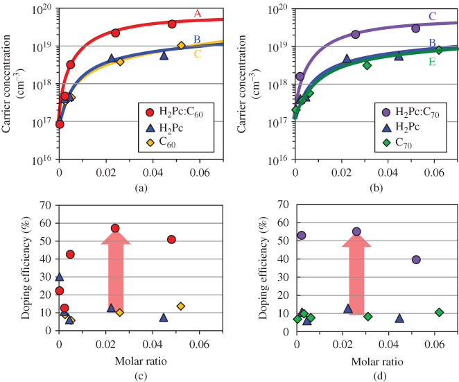
Figure 40 Dependence of carrier concentration and doping efficiency on Cs2CO3 doping concentration for H2Pc:C60 (a,b) and H2Pc:C70 (c,d) co-deposited films and their component films.
Shinmura et al., 2014 [53]. Reproduced with permission of American Institute of Physics.
Essentially, the same phenomenon was observed for acceptor doping. By combining H2Pc and Me-PTC, a considerable increase in doping efficiency to 30% was obtained from the 2% and 0.2% efficiencies obtained for H2Pc and Me-PTC films, respectively (Table II).5 Thus, we concluded that the increase in doping efficiency is universal and irrespective of whether the doping is donor or acceptor doping.
Table II Ionization Rates (Doping Efficiencies) of Co-deposited Films and Their Component Single Films and The Factor by Which the Doping Sensitization Has Increased for Donor-doped H2Pc:C60 and Acceptor-doped H2Pc:Me-PTC Systems
| Ionization Rate (Doping Efficiency) (%) | |||||
| Single Films | |||||
| Co-deposited Films | H2Pc | C60 | Me-PTC | Rate of Multiplication | |
| Donor doping (H2Pc:C60 system) | 50 | 10 | 10 | – | 10 |
| Acceptor doping (H2Pc:Me-PTC system) | 30 | 2 | – | 0.2 | 300 |
The doping process for Cs2CO3 in H2Pc can be explained by a CT complex, that is, the formation of H2Pc−–Cs2CO3+ and its ionization. Here, the positive charge on the Cs2CO3+ is a spatially fixed positive ion, that is, an ionized donor. The negative charge on the H2Pc is liberated by thermal energy and acts as a free electron in the CB (Fig. 41(a)). Thus, the doping efficiency can be expressed by the product of the rates of the CT complex formation and ionization. Since Cs2CO3 exists as a molecule having a structure of CsO(CO)OCs, it is reasonable to assume that Cs2CO3 evaporates molecularly and the rate of the CT complex formation with H2Pc, C60 and C60:H2Pc films is close to unity. Thus, we consider that the observed doping efficiency represents the ionization efficiency.
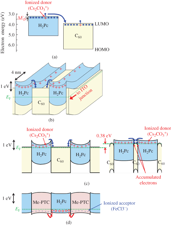
Figure 41 (a) Energy diagrams of Cs2CO3-doped H2Pc and C60 single films before contact. ΔED denotes the activation energy of the donors. Shinmura et al., 2014 [53]. Reproduced with permission of American Institute of Physics. (b) Three-dimensional energy structure for a Cs2CO3-doped H2Pc/C60 superlattice formed at an ITO interface after contact. Shinmura et al., 2014 [53]. Reproduced with permission of American Institute of Physics. (c) Cross-sectional energy structure of a Cs2CO3-doped H2Pc/C60 superlattice after contact, cut in parallel to the ITO interface after the end of the band-bending by ITO. The H2Pc:C60 ratios are 1:1 (left) and 99:1 (right). The gray shaded areas show the accumulated electrons in C60. (d) Cross-sectional energy structure of a FeCl3-doped Me-PTC/H2Pc superlattice after contact. The energy relationships are depicted on the same scale in all figures.
We propose a charge separation superlattice model to explain the enhancement in ionization rate. Figure 41(a) shows the energy structures of H2Pc and C60 single films before contact. The lower edge of the CB was determined by inverse photoelectron spectroscopy [68]. The activation energy (ΔED) of 0.12 eV was determined from the ionization rate of 10%.6 Before contact, 10% of the electrons are excited to the CB, and the other electrons are captured by donor levels (Fig. 41(a)).
By making contact with C60, since the electron transfer from the CB of H2Pc to that of C60 (Fig. 41(a)) occurs accompanied with energetic relaxation (0.7 eV), the electron concentration in H2Pc decreases. Due to the shift in equilibrium, electron liberation from the donor levels accelerates, that is, the ionization rate for donors increases only in the H2Pc region. Taking the molecular ratio of the H2Pc:C60 co-deposited film (1:1) into consideration, the ionization rate of the H2Pc region in the co-deposited film can be estimated to be 100%, while that in the C60 region is unchanged (10%), since the observed ionization rate of 55% for the H2Pc:C60 co-deposited film can be obtained by calculation, that is, 100% × 0.5 + 10% × 0.5 = 55%. Thus, we concluded that for the H2Pc region, the ionization rate increased from 10% to 100%, an increase by a factor of 10 (Table II). The ionization rate of 100% supports the assumption that the rate of formation of the CT complex is unity.
Figure 41(b) and (c) shows the three-dimensional and cross-sectional energy structures of charge separating H2Pc/C60 superlattices after contact, respectively. Due to the faster liberation of electrons from the donors, all of the donors in the H2Pc region of the co-deposited film positively ionize, and the energy band of H2Pc is bent to a depth of 3.3 nm.7 In this model, the H2Pc regions act as electron-supplying layers to the C60 regions. The C60 regions act as electron transporting highways. Based on this model, we expect that the total ionization rate in H2Pc:C60 co-deposited films would increase further by increasing the H2Pc ratio.
Figure 42(a) and (b) shows the Kelvin band-mapping results and observed ionization rates for different ratios of H2Pc in H2Pc:C60 co-deposited films doped with Cs2CO3. As the H2Pc ratio increases, the ionization rate increases proportionally, with good agreement to the calculated line (broken light grey line, Fig. 42(b)),8 and reached 97% at a H2Pc:C60 ratio of 99:1.
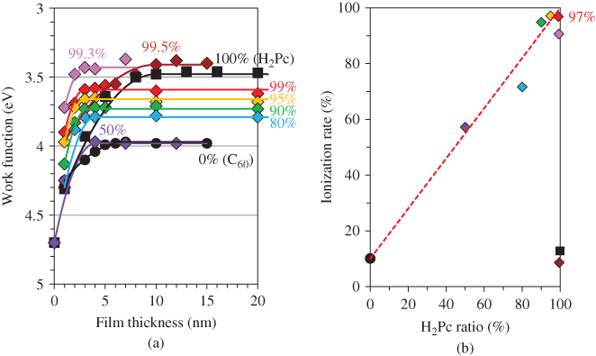
Figure 42 (a) Dependence of work function on the film thickness for various ratios of H2Pc in H2Pc:C60 co-deposited films doped with Cs2CO3 (MR = 0.02). Shinmura et al., 2014 [53]. Reproduced with permission of American Institute of Physics. (b) Ionization rate for various ratios of H2Pc in H2Pc:C60 co-deposited films. Calculated ionization rate is shown by the broken line.
Shinmura et al., 2014 [53]. Reproduced with permission of American Institute of Physics.
Interestingly, the positions of EF after band-bending systematically shift in the negative direction with decreasing C60 (Fig. 42(a)). This is a sign that there is a more concentrated accumulation of liberated electrons in the thinner C60 regions, which lifts EF by 0.38 eV for H2Pc:C60 (99:1) (compare the left and right plots in Fig. 41(c)). Since there should be a vast number of free electrons in the C60 CB under EF, we assume that a confined electron gas exists on the C60 sides of the H2Pc/C60 interfaces, similar to that reported for inorganic AlGaAs/GaAs superlattices [70]. This systematic observation also supports the proposed charge separation superlattice model.
For acceptor doping, the opposite mechanism occurs (Fig. 41(d)). Being in contact with H2Pc, the holes in the VB of Me-PTC energetically relax (0.3 eV) to the VB of H2Pc (dark grey arrows) and their concentration in Me-PTC decreases. As a result, there is faster liberation of holes from the acceptors. For the Me-PTC region, the ionization rate increases from 0.2% to 60%, a 300-fold increase (Table II).
Direct ionization processes might occur when the ionized donor is located just at the C60/H2Pc molecular interface (Fig. 43). For donors in the single C60 and H2Pc regions, the activation energy, that is, the binding energy of an electron around a positively ionized donor (Cs2CO3+) (ΔED) is 0.12 eV (Fig. 41(a)),6 which corresponds to an electron orbital radius of 1.6 nm (Fig. 43, circles A).9 This situation resembles the CT exciton. The only difference is that the positive charge of the ionized donor is fixed. For donors just on the H2Pc side of the C60/H2Pc molecular interface (Fig. 43, center), a cascade-like second electron transfer from the LUMO of the H2Pc molecule to that of the C60 molecule occurs (see Fig. 38). Compared to the binding energy (ΔED) of 0.12 eV, the relaxation energy of 0.58 eV10 is sufficient to liberate electrons by increasing the electron orbital radius to over 6.5 nm, which has a binding energy comparable to the thermal energy at room temperature (kT = 0.026 eV) (Fig. 43, semicircle B).11 This situation resembles the Wannier exciton. It should be noted that a similar electron transfer from H2Pc (D) to C60 (A) (Fig. 38) is utilized in organic solar cells to increase exciton dissociation, that is, so-called donor/acceptor (D/A) sensitization (Section III.B). Thus, the present doping sensitization phenomenon can be regarded as analogous to D/A sensitization for dopant ionization.
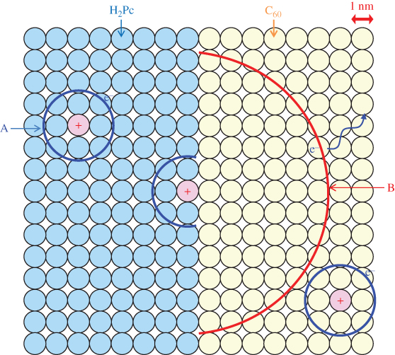
Figure 43 Schematic illustration of electron orbits around a positive ionized donor. The circles A are those for donors in single C60 and H2Pc regions. The semicircle B is that for a donor just on the H2Pc side of the H2Pc/C60 molecular interface.
Shinmura et al., 2014 [53]. Reproduced with permission of American Institute of Physics.
F. ppm-Doping Effects
The effects of doping reaching the 1 ppm level in organic photovoltaic cells were clarified using simple n+p-homojunctions [71]. With doping from 0 to 10 ppm, the FF increased due to the appearance of majority carriers. From 10 to 100 ppm, the photocurrent density increased due to the increase in the built-in potential, that is, the formation of an n+p-homojunction. The photocurrent was increased by a factor of 1.3 by directly doping the photoactive co-deposited layer with acceptors at 100 ppm.
We believe that direct doping of the photoactive co-deposited layer where the generation and transport of photocarriers occur has the potential to enhance the efficiency of these organic solar cells. Based on this consideration, we attempted to introduce a pn-homojunction into a C60:6T co-deposited film. For the simplest cell, we adopted an n+p-homojunction that has a one-sided abrupt junction (Fig. 44(a)) (Section V.D).
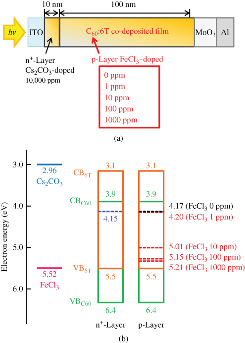
Figure 44 (a) Structure of n+p-homojunction cell having a one-sided abrupt junction. Ohashi et al., 2015 [71]. Reproduced with permission of Elsevier. (b) Energy band diagram of n+-C60:6T co-deposited films doped with Cs2CO3 (10,000 ppm) and that of p-C60:6T doped with FeCl3 (1, 10, 100, 1000 ppm) on an n+-layer. The positions of EF are shown by the broken lines. The work functions of Cs2CO3 and FeCl3 are also shown.
Ohashi et al., 2015 [71]. Reproduced with permission of Elsevier.
The Cs2CO3 doping concentration of the n+-layer was kept constant at 10,000 ppm. The FeCl3 doping concentrations of the p-layer were varied, that is, 0, 1, 10, 100, and 1000 ppm. The doping concentrations of 10 and 1 ppm were realized by reducing the dopant evaporation rate using rotating disks having slits with aperture ratios of 1/10 and 1/100, respectively. The doping concentration of 1 ppm corresponds to a molecular ratio (MR) of 3.7 × 10⁻⁶.
Figure 44(b) shows the energy diagram of the C60:6T co-deposited film. The bandgap in this film is determined by the CB of C60 (CBC60) and the VB of 6T (VB6T). In order to fabricate an n+-layer, heavy doping with Cs2CO3 (10,000 ppm) was performed. For the p-type layers formed on the n+-layer, FeCl3 doping concentrations of 10, 100, and 1000 ppm caused EF to shift toward VB6T (5.50 eV) with more positive values of 5.01, 5.15, and 5.21 eV, respectively. These observations suggest that an n+p-homojunction is expected to form as the FeCl3 concentration is gradually increased.
Figure 45 shows the current–voltage characteristics for n+p-homojunction cells with p-layer doping concentrations of 0, 1, 10, 100, and 1000 ppm (Fig. 44(a)). The magnitude of the short-circuit photocurrent density (Jsc) increases systematically with FeCl3 doping of the photoactive C60:6T layer as follows: 3.51 for 0 ppm, 4.02 for 10 ppm, and 4.48 mA/cm2 for 100 ppm. Simultaneously, the magnitude of the forward current density increases systematically (black, green, and red broken curves). That is, the cell resistance (Rs) decreases systematically with FeCl3 doping and the minimum Rs of 2.35 Ω cm2 is obtained at 100 ppm (see Fig. 47(b)). Jsc increases by a factor of 1.3 and the maximum efficiency of 1.51% is at 100 ppm. However Jsc decreases and Rs increases with a further increase in doping concentration to 1000 ppm. This confirms that the photocurrent can be increased significantly by directly doping the photoactive co-deposited layer with extremely low concentrations at the ppm level.

Figure 45 Current–voltage characteristics for n+p-homojunction cells having p-layer doping concentrations of 0, 1, 10, 100, and 1000 ppm. The photocurrent and darkcurrent are shown by solid and broken curves, respectively. The maximum efficiency was observed at 100 ppm (Jsc: 4.48 mA/cm2, Voc: 0.80 V, FF: 0.42, efficiency: 1.51%).
Ohashi et al., 2015 [71]. Reproduced with permission of Elsevier.
Band-bending occurs only on the p-side of the n+p-homojunction since the n+-layer is heavily doped (10,000 ppm) (see Section V.D). Therefore, the width of the depletion layer (Wdep) formed in the p-type layer depends on the FeCl3 doping concentration in the layer. Figure 46(a) shows the dependence of the work function on the p-type layer thickness for various doping concentrations. In the cases of 0 and 1 ppm, the observed work function has a constant value of 4.20 eV, which is the same as the Fermi level in the n+-layer, that is, no band-bending was observed. This shows that layers with these doping levels act as intrinsic layers. The observation that there was no change in work function at the extremely low concentration of 1 ppm doping (Fig. 46(a)) may be attributed to trap-filling, that is, the doping induced carriers are captured by the traps [72, 73]. In the cases of 10, 100, and 1000 ppm, band-bending was observed. This clearly shows that layers doped at these levels act as p-type layers. The width of the depletion layer (Wdep) and the built-in potential (Vbi) can be determined from the points (shown by arrows) at which band-bending ends. For example, Wdep = 50 nm and Vbi = 1.0 V at a doping concentration of 100 ppm. At 100 ppm, Nh was calculated to be 1.8 × 1017 cm−3. The dependences of Rs, Vbi, and Nh on doping concentration are shown in Fig. 47(b)–(d), respectively. The energy band diagrams of the n+p-homojunction cells (Fig. 46(b)) can be found by turning the curves in Fig. 46(a) upside down.

Figure 46 (a) The dependence of the work function on the p-layer thickness for various doping concentrations. p-layers were formed on n+-layers. Ohashi et al., 2015 [71]. Reproduced with permission of Elsevier.(b) Energy band diagrams of n+p-homojunction cells with 10, 100, and 1000 ppm FeCl3-doped p-layers.
Ohashi et al., 2015 [71]. Reproduced with permission of Elsevier.

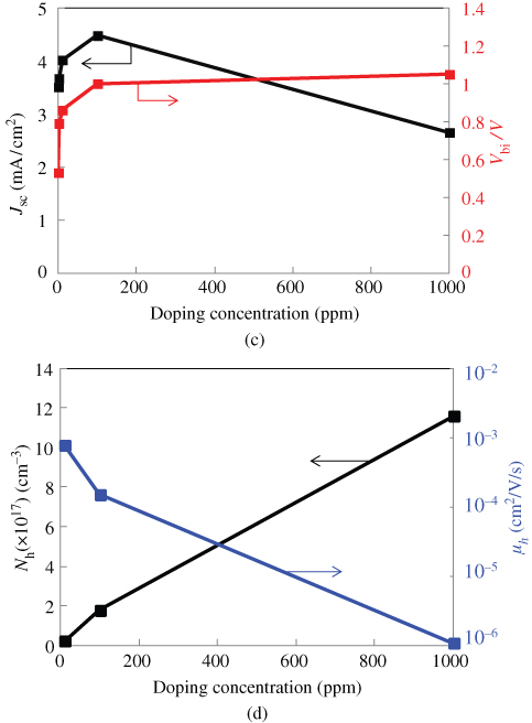
Figure 47 (a) Dependences of Jsc and fill-factor (FF) on doping concentration. Ohashi et al., 2015 [71]. Reproduced with permission of Elsevier. (b) Dependences of fill-factor (FF) and cell resistance (Rs) on doping concentration. Ohashi et al., 2015 [71]. Reproduced with permission of Elsevier. (c) Dependences of Jsc and built-in potential (Vbi) on doping concentration. Ohashi et al., 2015 [71]. Reproduced with permission of Elsevier. (d) Dependences of hole concentration (Nh) and hole mobility (μh) on doping concentration.
Ohashi et al., 2015 [71]. Reproduced with permission of Elsevier.
Figure 47(a) shows the dependences of Jsc and the FF on doping concentration. The doping effects can be divided into three regions. From 0 to 10 ppm, both FF and Jsc increase rapidly. From 10 to 100 ppm, Jsc still increases while FF maintains a constant value. From 100 to 1000 ppm, both Jsc and FF decrease.
Figure 47(b) shows the dependences of the FF and the cell resistance (Rs) on doping concentration from 0 to 100 ppm. Clearly, Rs decreases and FF increases from 0 to 10 ppm. Once acceptor doping is performed, holes and electrons inevitably act as majority carriers and minority carriers, respectively. At 10 ppm, the number (Nh) of majority carriers (holes) is 2.3 × 1016 cm−3. Thus, we conclude that the increase in FF at 10 ppm doping is due to the appearance of majority carriers in the p-layer.
Figure 47(c) shows the dependences of Jsc and the built-in potential (Vbi) on doping concentration from 0 to 1000 ppm. Clearly, there is a close relationship between Jsc and Vbi. In particular, there are simultaneous increases in Jsc and Vbi at relatively low doping concentrations from 10 to 100 ppm. An increase in Vbi is also shown in the energy band diagrams for 10 and 100 ppm in Fig. 46(b), and one can see that Jsc increases with increasing Vbi. Based on these considerations, we conclude that the increase in Jsc is due to the increase in Vbi, that is, the formation of an n+p-homojunction.
From 100 to 1000 ppm, both FF and Jsc decrease (Fig. 47(a)). Simultaneously, Rs increases considerably from 2.35 to 50 Ω cm2. The mobility of the majority carriers (holes), μh, can be calculated based on Eq. (3.7)
Here, Nh and σh are the hole concentration, which is obtained by Kelvin band-mapping (Fig. 46(a)) and the hole conductivity, which is obtained from the cell resistance (σh = LRs−1; L: cell thickness) determined from the forward dark current for the n+p-homojunction cells (n+-C60:6T/p-C60:6T/MoO3) (Fig. 45, broken curves), respectively. The mobility, μh, was calculated to be 1.5 × 10⁻⁴ and 1.1 × 10⁻⁶ cm2/V/s at 100 and 1000 ppm, respectively. Figure 47(d) shows the dependences of the hole concentration (Nh) and the hole mobility (μh) on doping concentration from 10 to 1000 ppm. μh decreases at higher concentrations from 100 to 1000 ppm (light grey solid curve). We think this is due to the disturbance of hopping transport of holes by the negatively ionized and neutral accepter dopants, although there still remains the possibility that it is due to a change in morphology on the nanoscale. Harada et al. [74, 75] reported decreasing mobility for higher doping concentrations in C60 films. The decrease in μh dominates the cell resistance (Rs) in spite of the increase in Nh, causing Rs to increase and, as a result, FF to decrease. Thus, we conclude that the decrease in FF is due to the decrease in hole mobility (μh). As shown in Fig. 46(b), the width of the depletion layer (Wdep) reduces from 50 to 20 nm as the doping concentration is increased from 100 to 1000 ppm. Thus, we conclude that the decrease in Jsc is due to the decrease in Wdep, which acts as the photoactive layer.
In conclusion, by directly doping a photoactive co-deposited layer at the ppm level, we were able to increase both the photocurrent and the FF. The increases in FF and Jsc from 0 to 100 ppm are due to the decrease in Rs following the introduction of majority carriers and the increase in Vbi, respectively. The decreases in FF and Jsc from 100 to 1000 ppm doping are caused by the decrease in mobility of the majority carriers and by the decrease in Wdep, respectively. The most important technical consequence of this doping is possibility for the intentional design of built-in potentials in cells. We think that a new design concept including this doping technology should be developed to realize a high-performance cell.
VI. Conclusion
The basic principles of organic solar cells, that is, excitons, D/A sensitization, exciton diffusion, blended junctions, nanostructure design, and energetic structure design are summarized. Especially, nanostructure design, that is, vertical superlattices and phase separation, and energetic structure design, that is, 7N purification, methods for ppm-level doping, pn-control for single and D/A co-deposited organic semiconductors, junction formation, doping sensitization, and ppm-doping effects for small-molecular-type organic solar cells, are discussed.
The author believes that the science of doping in organic semiconductors is indispensable to the development of organic solar cells, which have the potential to provide the next generation of low-cost solar cells.
Organic solar cells are representative of the organic electronics industry, which includes organic electroluminescent devices and organic transistors, and is set to dominate in the twenty-first century, following on from the dominance of the inorganic electronics industry in the twentieth century. The field of organic solar cells is closely related to many other research fields such as device physics, electronics, and synthetic chemistry, in which there are a vast number of researchers.
The author fervently hopes that young researchers will take up the challenge of working in the interdisciplinary field of organic solar cells to help develop the next generation of cells for renewable energy. Some suggested books for young researchers are indicated [76–79].
Acknowledgments
Funding from Core Research for Evolutional Science and Technology (CREST) from the Japan Science and Technology Agency (JST) is gratefully acknowledged. The author expresses great appreciation to members of the Hiramoto Group in the Institute for Molecular Science, M. Kubo (PhD, CREST researcher), Y. Shinmura (PhD, CREST researcher), Y. Yamashina (CREST researcher), N. Ishiyama (PhD student), C. Ohashi (PhD student), and T. Kaji (Assistant Prof.) for accomplishing the present researches. The author thanks M. Izaki (Prof., Toyohashi Univ. Tech.) for measurements of C60 purity. The author also thanks A. Adachi and S. Ohashi of Epitech Co. for the design and construction of the ppm-doping apparatus.
References
- 1. Kearns, D. and Calvin, M. (1958) J. Chem. Phys., 29, 950.
- 2. Ghosh, A.K., Morel, D.L., Feng, T. et al. (1974) J. Appl. Phys., 45, 230.
- 3. Ghosh, A.K. and Feng, T. (1978) J. Appl. Phys., 49, 5982.
- 4. Chamberlain, G.A. (1983) Solar Cells, 8, 47, and references therein.
- 5. Wohrle, D. and Meissner, D. (1991) Adv. Mater., 3, 129, and references therein..
- 6. Tang, C.W. (1986) Appl. Phys. Lett., 48, 183.
- 7. Hiramoto, M., Fujiwara, H., and Yokoyama, M. (1991) Appl. Phys. Lett., 58, 1062.
- 8. Hiramoto, M., Fujiwara, H., and Yokoyama, M. (1992) J. Appl. Phys., 72, 3787.
- 9. Sariciftci, N.S., Smilowitz, L., Heeger, A.J., and Wudl, F. (1992) Science, 285, 1474.
- 10. Yu, G., Gao, J., Hummelen, J.C. et al. (1995) Science, 270, 1789.
- 11. Peumans, P., Yakimov, A., and Forrest, S.R. (2003) J. Appl. Phys., 93, 3693.
- 12. Hiramoto, M., Yamaga, T., Danno, M. et al. (2006) Appl. Phys. Lett., 88, 213105.
- 13. O'Regan, B. and Grätzel, M. (1991) Nature, 353, 737.
- 14. Matsuo, Y., Sato, Y., Niinomi, T. et al. (2009) J. Am. Chem. Soc., 131, 16048.
- 15. Hiramoto, M. (2006) Electron. Comm. Jpn. Part 2, 89, 13–18.
- 16. Kaji, T., Zhang, M., Nakao, S. et al. (2011) Adv. Mat., 23, 3320.
- 17. http://www.m-kagaku.co.jp/newsreleases/00018.html.
- 18. Wagner, H.J., Loutfy, R.O., and Hsiao, C. (1982) J. Mater. Sci., 17, 2781.
- 19. Laudise, R.A., Kloc, C., Simpkins, P.G., and Siegrist, T. (1998) J. Cryst. Growth, 187, 449.
- 20. Suemori, K., Miyata, T., Yokoyama, M., and Hiramoto, M. (2004) Appl. Phys. Lett., 85, 6269.
- 21. Surmori, K., Yokoyama, M., and Hiramoto, M. (2006) J. Appl. Phys., 99, 036109.
- 22. Suemori, K., Miyata, T., Yokoyama, M., and Hiramoto, M. (2005) Appl. Phys. Lett., 86, 063509.
- 23. Sakai, K. and Hiramoto, M. (2008) Mol. Cryst. Liq. Cryst., 491, 284.
- 24. Hiramoto, M. (2008) Efficient Organic p-i-n Solar Cells Having Very Thick Co-deposited i-Layers Composed of Highly Purified Organic Semiconductors, Proceedings of SPIE Vol. 7052, Organic Photovoltaics IX, August 12–14 (70520H), San Diego, CA, USA.
- 25. Brenninghoven, A., Rundenauer, F.G., and Werner, H.W. (1987) Secondary Ion Mass Spectrometry, John Wiley & Sons.
- 26. Tanaka, Y., Kanai, K., Ouchi, Y., and Seki, K. (2007) Chem. Phys. Lett., 441, 63.
- 27. Martin, M., Andre, J.-J., and Simon, J. (1983) J. Appl. Phys., 54, 2792.
- 28. Tada, H., Touda, H., Takada, M., and Matsushige, K. (2000) Appl. Phys. Lett., 2000 (76), 873.
- 29. Akamatsu, H., Inokuchi, H., and Matsunaga, Y. (1954) Nature, 173, 168.
- 30. Hiramoto, M., Ihara, K., Fukusumi, H., and Yokoyama, M. (1995) J. Appl. Phys., 78, 7153.
- 31. Hiramoto, M., Ihara, K., and Yokoyama, M. (1995) Jpn. J. Appl. Phys., 34, 3803.
- 32. Huang, S.J., Pfeiffer, M., Werner, A. et al. (2002) Appl. Phys. Lett., 80, 139.
- 33. Blochwitz, J., Pfeiffer, M., Fritz, T., and Leo, K. (1998) Appl. Phys. Lett., 73, 729.
- 34. Solomeshch, O., Yu, Y.J., Goryunkov, A.A. et al. (2009) Adv. Mater., 21, 4456.
- 35. Tokito, S., Noda, K., and Taga, Y. (1996) J. Phys. D: Appl. Phys., 29, 2750.
- 36. Matsushima, T., Kinoshita, Y., and Murata, H. (2007) Appl. Phys. Lett., 91, 253504-1-3.
- 37. Harada, K., Werner, A.G., Pfeiffer, M. et al. (2005) Phys. Rev. Lett., 94, 036601-1-4.
- 38. Chan, C.K., Zhao, W., Barlow, S. et al. (2008) Org. Electron., 9, 575.
- 39. Harada, K., Riede, M., and Leo, K. (2008) Phys. Rev. B, 77, 195212-1-9.
- 40. Liao, H.-H., Chen, L.-M., Xu, Z. et al. (2008) Appl. Phys. Lett., 92, 173303.
- 41. Hamwi, S., Riedl, T., and Kowalsky, W. (2011) Appl. Phys. Lett., 99, 053301-1-3.
- 42. Chan, C.K., Amy, F., Zhang, Q. et al. (2006) Chem. Phys. Lett., 431, 67.
- 43. Walzer, K., Maennig, B., Pfeiffer, M., and Leo, K. (2007) Chem. Rev., 107, 1233, and references therein.
- 44. Hiramoto, M., Kubo, M., Shinmura, Y. et al. (2014) Electronics, 3, 351–380.
- 45. Falkenberg, C., Uhrich, C., Olthof, S. et al. (2008) J. Appl. Phys., 104, 034506-1-6.
- 46. Yoshida, H. (2013) Rev. Sci. Instrum., 84, 103901-1-5.
- 47. Kubo, M., Iketaki, K., Kaji, T., and Hiramoto, M. (2011) Appl. Phys. Lett., 98, 073311-1-3.
- 48. Kubo, M., Kaji, T., and Hiramoto, M. (2011) AIP Advances, 1, 032177-1-5.
- 49. Ishiyama, N., Kubo, M., Kaji, T., and Hiramoto, M. (2012) Appl. Phys. Lett., 101, 233303-1-3.
- 50. Shinmura, Y., Kubo, M., Ishiyama, N. et al. (2012) AIP Advances, 2, 032145-1-6.
- 51. Hamwi, S., Meyer, J., Winkler, T. et al. (2009) Appl. Phys. Lett., 94, 253307-1-3.
- 52. Ishiyama, N., Kubo, M., Kaji, T., and Hiramoto, M. (2011) Appl. Phys. Lett., 99, 133301-1-3.
- 53. Shinmura, Y., Yamashina, Y., Kaji, T., and Hiramoto, M. (2014) Appl. Phys. Lett., 105, 183306.
- 54. Hebard, F.A., Hadon, C.R., Fleming, M.R., and Kortan, R.A. (1991) Appl. Phys. Lett., 59, 2109.
- 55. Kröger, M., Hamwi, S., Meyer, J. et al. (2009) Org. Electron., 10, 932.
- 56. deMello, J.C., Tessler, N., Graham, S.C., and Friend, R.H. (1998) Phys. Rev. B, 57, 12951.
- 57. Hiramoto, M., Tomioka, A., Suemori, K., and Yokoyama, M. (2004) Appl. Phys. Lett., 85, 1852.
- 58. Kubo, M., Shinmura, Y., Ishiyama, N. et al. (2012) Appl. Phys. Express, 5, 092302-1-3.
- 59. Kubo, M., Kaji, T., and Hiramoto, M. (2013) Appl. Phys. Lett., 103, 263303-1-4.
- 60. Kubo, M., Shinmura, Y., Ishiyama, N. et al. (2013) Mol. Cryst. Liq. Cryst., 581, 13.
- 61. Ishiyama, N., Kubo, M., Kaji, T., and Hiramoto, M. (2013) Org. Electron., 14, 1793.
- 62. Hiramoto, M., Suezaki, M., and Yokoyama, M. (1990) Chem. Lett., 19, 327.
- 63. Yuan, Y., Huang, J., and Li, G. (2011) Green, 1, 65.
- 64. Yamashina, Y., Shinmura, Y., Ishiyama, N. et al. (2015) J. Appl. Phys., 117, 125501.
- 65. Sze, S.M. (1969) Physics of Semiconductor Devices, Wiley, New York.
- 66. Ishiyama, N., Yoshioka, T., Kaji, T., and Hiramoto, M. (2013) Appl. Phys. Express, 6, 012301.
- 67. Yoshida, H. (2014) Anal. Bioanal. Chem., 406, 2231 and H. Yoshida (private communication).
- 68. Yoshida, H. (2012) Chem. Phys. Lett., 539–540, 180.
- 69. Ishii, H., Sugiyama, K., Ito, E., and Seki, K. (1999) Adv. Mater., 11, 605.
- 70. Dingle, R., Stormer, H.L., Gossard, A.C., and Wiegmann, W. (1978) Appl. Phys. Lett., 33, 665.
- 71. Ohashi, C., Shinmura, Y., Kubo, M., and Hiramoto, M. (2015) Org. Electron., 27, 151.
- 72. Tietze, M.L., Pahner, P., Schmidt, K. et al. (2015) Adv. Funct. Mater., 25, 2701.
- 73. Olthof, S., Mehraeen, S., Mohapatra, S.K. et al. (2012) Phys. Rev. Lett., 109, 176601.
- 74. Harada, K., Li, F., Maennig, B. et al. (2007) Appl. Phys. Lett., 91, 092118.
- 75. Harada, K., Sumino, M., Adachi, C. et al. (2010) Appl. Phys. Lett., 96, 253304.
- 76. Brabec, C., Dyakonov, V., and Scherf, U. (eds) (2008) Organic Photovoltaics, Materials, Device Physics, and Manufacturing Technologies, Wiley-VCH Verlag GmbH & Co. KGaA, Weinheim.
- 77. Stability and Degradation of Organic and Polymer Solar Cells; F. C. Krebs, Ed.; John Wiley & Sons: West Sussex, 2012.
- 78. Hoth, C., Seemann, A., Steim, R. et al. (2014) Printed organic solar cells, in Solar Cell Materials, Developing Technologies, John Wiley & Sons, West Sussex, pp. 217–282.
- 79. Organic Photovoltaics, Mechanisms, Materials, and Devices; S.-S. Sun and N. S. Sariciftci, Ed.; Taylor & Francis: London, 2005.