
Chapter 8
Advanced Transimpedance Amplifier Design II
In the following, we explore ways to reduce the noise by replacing the noisy feedback resistor of the shunt-feedback TIA with a capacitive, optical, or active-feedback device. Then, we discuss the current-mode TIA in which the voltage amplifier is replace by a current amplifier. After that, we look at photodetector bootstrapping, a technique to reduce the detector's effective capacitance. Finally, we turn to TIAs for specialized applications, such as burst-mode receivers and analog receivers.
8.1 TIA with Nonresistive Feedback
Capacitive-Feedback TIA with Differentiator
In medium- and low-speed applications, a large portion of the TIA's input-referred noise current originates from the feedback resistor(s) (cf. Section 6.3). In principle, we can get rid of this noise by replacing the feedback resistor with a noise-free feedback capacitor. But unfortunately, this replacement turns the TIA into an integrator, which severely distorts the signal waveforms.
One solution to this problem is to follow the integrator with a differentiator, as shown in Fig. 8.1(a), thus equalizing the frequency response [1, 2]. Assuming large voltage gains for ![]() and
and ![]() , the low-frequency transimpedance of this circuit is [1]
, the low-frequency transimpedance of this circuit is [1]

and its input-referred noise current PSD due to ![]() is [1]
is [1]

Equation (8.1) suggests that the integrator–differentiator circuit can be re-interpreted as a current amplifier consisting of ![]() ,
, ![]() , and
, and ![]() with current gain
with current gain ![]() followed by a resistive shunt-feedback TIA consisting of
followed by a resistive shunt-feedback TIA consisting of ![]() and
and ![]() . Comparing Eqs (8.1) and (8.2), we find that for
. Comparing Eqs (8.1) and (8.2), we find that for ![]() the noise due to
the noise due to ![]() is lower than that of the equivalent resistive-feedback TIA. For example, for
is lower than that of the equivalent resistive-feedback TIA. For example, for ![]() , the noise contribution of the capacitive-feedback TIA is
, the noise contribution of the capacitive-feedback TIA is ![]() , whereas the noise contribution of the equivalent resistive-feedback TIA with
, whereas the noise contribution of the equivalent resistive-feedback TIA with ![]() is
is ![]() , which is twice as large.
, which is twice as large.
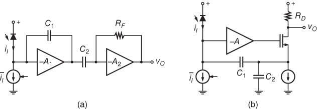
Figure 8.1 TIAs with capacitive feedback: (a) integrator–differentiator and (b) current-divider configuration.
The main drawback of this arrangement is that the integrator quickly saturates (overloads) for input signals that contain a DC component. This issue can be avoided by adding a DC input current control circuit that removes the average input current, ![]() , from the input signal, as indicated with the current source in Fig. 8.1(a). (A feedback circuit similar to that in Fig. 7.11 can be used to control the current source.) Alternatively, a large resistor in parallel to
, from the input signal, as indicated with the current source in Fig. 8.1(a). (A feedback circuit similar to that in Fig. 7.11 can be used to control the current source.) Alternatively, a large resistor in parallel to ![]() [1] can provide some tolerance to DC currents. Unfortunately, both of these methods add noise.
[1] can provide some tolerance to DC currents. Unfortunately, both of these methods add noise.
Another drawback, familiar from the high-impedance front-end (cf. Section 6.1), is that the integrator saturates for long runs of zeros or ones, making it impossible for the differentiator to recover the original signal waveform.
The main application of the integrator–differentiator circuit in Fig. 8.1(a) has been for high-sensitivity current probes [1, 2].
Capacitive-Feedback TIA with Current Divider
Another capacitive-feedback circuit, which has been proposed with optical receivers in mind [3, 4] and also has found application in microelectromechanical systems (MEMS) [5], is shown in Fig. 8.1(b). This circuit produces an AC drain current that is ![]() times larger than the AC input current
times larger than the AC input current ![]() . To understand the origin of this gain, consider that the currents through
. To understand the origin of this gain, consider that the currents through ![]() and
and ![]() must sum up to the AC drain current and that, given a virtual ground at the input of the voltage amplifier, the ratio of these two currents must be
must sum up to the AC drain current and that, given a virtual ground at the input of the voltage amplifier, the ratio of these two currents must be ![]() to
to ![]() . Thus, the AC drain current is divided into two parts, with the part through
. Thus, the AC drain current is divided into two parts, with the part through ![]() being equal to
being equal to ![]() and the part through
and the part through ![]() being equal to
being equal to ![]() . Finally, the load resistor
. Finally, the load resistor ![]() converts the drain current into a voltage, making this circuit a TIA.
converts the drain current into a voltage, making this circuit a TIA.
Assuming a large voltage gain ![]() , the low-frequency transimpedance of this circuit is [3, 5]
, the low-frequency transimpedance of this circuit is [3, 5]

and its input-referred noise current PSD due to ![]() is [5]
is [5]

Comparing Eqs. (8.3) and (8.4), we find that for ![]() , the noise due to
, the noise due to ![]() is lower than that of a simple common-gate TIA with the same transimpedance. But like the integrator–differentiator circuit, this circuit also suffers from intolerance to DC input currents, necessitating a DC input current control circuit [3]. Although this TIA does not contain an explicit integrator, the voltage amplifier output follows the integral of the input current and thus is susceptible to saturation when long runs of zeros or ones occur.
is lower than that of a simple common-gate TIA with the same transimpedance. But like the integrator–differentiator circuit, this circuit also suffers from intolerance to DC input currents, necessitating a DC input current control circuit [3]. Although this TIA does not contain an explicit integrator, the voltage amplifier output follows the integral of the input current and thus is susceptible to saturation when long runs of zeros or ones occur.
Note that the integrate-and-dump receiver that we discussed in Section 4.9 can be realized as a TIA with capacitive feedback and a reset switch [6]. In this case, the saturation problem is resolved by periodically discharging the feedback capacitor.
Optical-Feedback TIA
Another way to eliminate the noise of the feedback resistor is to replace it with an optical-feedback scheme [7, 8]. This approach is illustrated in Fig. 8.2. The voltage amplifier drives a light-emitting diode (LED) through the series resistor ![]() , producing an optical feedback signal. This optical signal illuminates a p–i–n photodetector, generating an electrical current that is approximately proportional to
, producing an optical feedback signal. This optical signal illuminates a p–i–n photodetector, generating an electrical current that is approximately proportional to ![]() . Assuming a large voltage gain
. Assuming a large voltage gain ![]() , the current from the feedback photodetector tracks the current
, the current from the feedback photodetector tracks the current ![]() from the input photodetector.
from the input photodetector.
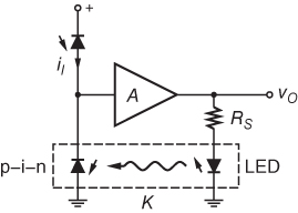
Figure 8.2 TIA with optical feedback.
The entire optical feedback path can be described by the coupling factor ![]() , defined as the ratio of the small-signal p–i–n photodetector current to the small-signal LED current (thus
, defined as the ratio of the small-signal p–i–n photodetector current to the small-signal LED current (thus ![]() is the product of the quantum efficiency of the p–i–n detector, the differential quantum efficiency of the LED, and the coupling loss from the LED to the p–i–n detector). Typical values for
is the product of the quantum efficiency of the p–i–n detector, the differential quantum efficiency of the LED, and the coupling loss from the LED to the p–i–n detector). Typical values for ![]() are in the range
are in the range ![]() to
to ![]() . The low-frequency transimpedance of the optical-feedback TIA is [8]
. The low-frequency transimpedance of the optical-feedback TIA is [8]
and its input-referred noise current PSD due to ![]() is [8]
is [8]

For ![]() , which is easy to realize, the noise due to
, which is easy to realize, the noise due to ![]() is lower than that of a resistive shunt-feedback TIA with the same transimpedance.
is lower than that of a resistive shunt-feedback TIA with the same transimpedance.
A detailed analysis [8] shows that optical feedback offers an improved dynamic range over resistive feedback for bit rates up to a few hundred megabits per second, with the exact crossover point depending on the value of ![]() .
.
The optical-feedback TIA also has the advantage of a very low parasitic feedback capacitance ![]() [8]. The bandwidth of TIAs with large feedback resistors and high amplifier gains is often limited by the parasitic feedback capacitance. For the optical-feedback TIA, this capacitance can be made arbitrarily small by increasing the spacing between the LED and the p–i–n photodiode (
[8]. The bandwidth of TIAs with large feedback resistors and high amplifier gains is often limited by the parasitic feedback capacitance. For the optical-feedback TIA, this capacitance can be made arbitrarily small by increasing the spacing between the LED and the p–i–n photodiode (![]() of fiber are used in [8]).
of fiber are used in [8]).
The main drawbacks of optical feedback are the cost and board space taken up by the optocoupler, which cannot be integrated in a standard technology.
The aforementioned optical-feedback scheme takes advantage of the fact that a resistor ![]() connected in series with an ideal current attenuator
connected in series with an ideal current attenuator ![]() has the effective resistance
has the effective resistance ![]() for signals but the
for signals but the ![]() times larger resistance
times larger resistance ![]() for noise. Current attenuators realized in the electrical rather than the optical domain can achieve a similar effect [2]. Note that the current attenuator requires a third terminal and thus it is not possible to build a two-terminal resistor with less noise than required by physics.
for noise. Current attenuators realized in the electrical rather than the optical domain can achieve a similar effect [2]. Note that the current attenuator requires a third terminal and thus it is not possible to build a two-terminal resistor with less noise than required by physics.
Active-Feedback TIA
In yet another variation of the shunt-feedback TIA, the feedback resistor ![]() is replaced by a transistor. The feedback transistor can be a FET or a BJT. In either case there are three different feedback configurations: common source, common drain, or common gate for the FET case and common emitter, common collector, or common base for the BJT case.
is replaced by a transistor. The feedback transistor can be a FET or a BJT. In either case there are three different feedback configurations: common source, common drain, or common gate for the FET case and common emitter, common collector, or common base for the BJT case.
In the following we look at active-feedback TIAs based on a common-source and a common-drain feedback device in more detail. TIAs based on a common-gate (common-base) feedback device [9] are less common.
Common-Source Feedback Device
The basic circuit with a common-source feedback device is shown in Fig. 8.3(a) [10, 11]. Note that the FET here does not act as a variable resistor like in Fig. 7.14(a), but as a voltage-controlled current source (transconductor) driven by the TIA output voltage and injecting a current into the TIA input. This type of feedback is known as active feedback [11, 12]. To obtain negative feedback through the inverting ![]() , the voltage amplifier must be of the noninverting type. It can be implemented, for example, with two cascaded common-source (common-emitter) stages [11] or a combination of common-gate (common-base) and common-drain (common-collector) stages [12–14].
, the voltage amplifier must be of the noninverting type. It can be implemented, for example, with two cascaded common-source (common-emitter) stages [11] or a combination of common-gate (common-base) and common-drain (common-collector) stages [12–14].

Figure 8.3 TIA with active feedback through an n-MOS device: (a) common-source and (b) common-drain configuration.
The low-frequency transimpedance of the common-source active-feedback TIA is [10, 11] (cf. Eq. (I.145))
and its input-referred noise current PSD due to ![]() is (cf. Eq. (I.147))
is (cf. Eq. (I.147))
where ![]() is the transconductance of
is the transconductance of ![]() ,
, ![]() (cf. Section 6.3), and we neglected the output conductance of
(cf. Section 6.3), and we neglected the output conductance of ![]() . The low-frequency input resistance is
. The low-frequency input resistance is ![]() . If we take
. If we take ![]() as frequency independent, the TIA's bandwidth becomes
as frequency independent, the TIA's bandwidth becomes ![]() , where
, where ![]() is the total capacitance at the input node [10, 11]. If we model
is the total capacitance at the input node [10, 11]. If we model ![]() as a first-order low-pass and place the pole such that the TIA assumes a second-order Butterworth response, the bandwidth increases by
as a first-order low-pass and place the pole such that the TIA assumes a second-order Butterworth response, the bandwidth increases by ![]() over the frequency-independent case (cf. Eq. (I.146)). [
over the frequency-independent case (cf. Eq. (I.146)). [![]() Problem 8.1.]
Problem 8.1.]
If we replace the noninverting amplifier in Fig. 8.3(a) with a simple wire (![]() ), we end up with a gate-drain connected FET. This degenerate form of the active-feedback TIA can serve as a receiver front-end in the same way a simple resistor can serve as a low- or high-impedance front-end [15].
), we end up with a gate-drain connected FET. This degenerate form of the active-feedback TIA can serve as a receiver front-end in the same way a simple resistor can serve as a low- or high-impedance front-end [15].
Common-Drain Feedback Device
Active feedback through a common-drain device is shown in Fig. 8.3(b) [16–18]. This arrangement requires an inverting voltage amplifier, just like in the case of resistive feedback. Here, ![]() acts as a voltage-controlled current source producing a feedback current that depends on the voltage difference
acts as a voltage-controlled current source producing a feedback current that depends on the voltage difference ![]() . Note the close analogy to resistive feedback for which the feedback current is given by
. Note the close analogy to resistive feedback for which the feedback current is given by ![]() .
.
The low-frequency transimpedance of the common-drain active-feedback TIA is (cf. Eq. (I.150))

and its input-referred noise current PSD due to ![]() is (cf. Eq. (I.153))
is (cf. Eq. (I.153))
where we neglected the bulk transconductance, output conductance, and induced gate noise of ![]() . The low-frequency input resistance is
. The low-frequency input resistance is  [16], which happens to be the same expression as for the regulated-cascode TIA. Note the similarity between this active-feedback TIA and the regulated-cascode TIA, the main difference being that the output signal is taken from the booster amplifier's output rather than the input FET's drain. The frequency response and bandwidth of this active-feedback TIA are identical to those of the resistive feedback TIA, if we substitute
 ![]() by
by ![]() (and neglect
(and neglect ![]() ,
, ![]() , and
, and ![]() of
of ![]() ). [
). [![]() Problem 8.2.]
Problem 8.2.]
Active Feedback versus Resistive Feedback
The active-feedback TIA potentially is less noisy at low frequencies than the resistive-feedback TIA [19]. To realize this noise advantage, ![]() must be less than one, a condition that occurs for long-channel devices where theoretically
must be less than one, a condition that occurs for long-channel devices where theoretically ![]() . If we replace
. If we replace ![]() with a BJT, the noise due to the feedback device is lower than that of the corresponding feedback resistor if
with a BJT, the noise due to the feedback device is lower than that of the corresponding feedback resistor if ![]() , where
, where ![]() is the base resistance of the feedback BJT [20] (cf. Eq. (I.148)). Another advantage of the active-feedback TIA is that the voltage amplifier needs to drive only the small capacitive load presented by
is the base resistance of the feedback BJT [20] (cf. Eq. (I.148)). Another advantage of the active-feedback TIA is that the voltage amplifier needs to drive only the small capacitive load presented by ![]() .
.
On the downside, active feedback tends to result in a higher total capacitance ![]() at the input and more high-frequency (
at the input and more high-frequency ( ![]() ) noise than resistive feedback.
) noise than resistive feedback.
Furthermore, active feedback is less linear than resistive feedback which may be a disadvantage (because of signal distortions) or an advantage (because of desirable signal compression) depending on the application. If linearity is important, the active-feedback TIA can be followed by a nonlinearity that cancels the feedback nonlinearity. In the case of common-source (or common-emitter) active feedback this is easily implemented by driving a matched common-source (or common-emitter) transistor from the voltage amplifier output [19, 20].
Besides the optical receiver application shown in Fig. 8.3, active-feedback TIAs also find application in wideband LNAs for wireless applications [16–18], MEMS [13], and as load elements in broadband amplifier stages [21–23].
8.2 Current-Mode TIA
What happens if we replace the voltage amplifier in the shunt-feedback TIA with a current amplifier, as shown in Fig. 8.4? The current amplifier senses the input current, ![]() , with a low-impedance input (
, with a low-impedance input (![]() ) and outputs the amplified current,
) and outputs the amplified current, ![]() , at a high-impedance output (
, at a high-impedance output (![]() ). Circuits like this, where signals are represented by currents rather than voltages, are called current-mode circuits.
). Circuits like this, where signals are represented by currents rather than voltages, are called current-mode circuits.

Figure 8.4 Shunt-feedback TIA with current amplifier.
Simple Analysis
Let us assume for now that the current amplifier has a high gain, ![]() . Then, for the output current to remain finite, the input current must stay close to zero. Like a voltage amplifier has a small input voltage (virtual ground), a current amplifier has a small input current (“virtual open”) when negative feedback is applied and the loop gain is high. Thus, almost all of the photodetector current
. Then, for the output current to remain finite, the input current must stay close to zero. Like a voltage amplifier has a small input voltage (virtual ground), a current amplifier has a small input current (“virtual open”) when negative feedback is applied and the loop gain is high. Thus, almost all of the photodetector current ![]() flows into
flows into ![]() . With the input voltage of the current amplifier being close to zero (grounded through
. With the input voltage of the current amplifier being close to zero (grounded through ![]() ), the output voltage becomes
), the output voltage becomes ![]() . Interestingly, no matter whether a (high-gain) voltage amplifier or a (high-gain) current amplifier is used, the overall transimpedance is the same and is determined only by the feedback element
. Interestingly, no matter whether a (high-gain) voltage amplifier or a (high-gain) current amplifier is used, the overall transimpedance is the same and is determined only by the feedback element ![]() .
.
There are however two interesting differences: First, whereas the voltage-mode TIA features a low input impedance only as a result of the feedback action, the current-mode TIA has a low input impedance even before feedback is applied [24, 25] (feedback reduces it further). This feature promises a strong suppression of the total capacitance at the input (![]() ), resulting in a low sensitivity to the photodetector capacitance
), resulting in a low sensitivity to the photodetector capacitance ![]() .
.
Second, whereas the AC feedback current in the voltage-mode TIA decreases with increasing ![]() , the current source output of the current-mode TIA forces a feedback current that is independent of
, the current source output of the current-mode TIA forces a feedback current that is independent of ![]() (neglecting
(neglecting ![]() ). As a result, the TIA's bandwidth becomes independent of
). As a result, the TIA's bandwidth becomes independent of ![]() and
and ![]() . This property is called gain-bandwidth independence [24, 25]. We return to this topic later.
. This property is called gain-bandwidth independence [24, 25]. We return to this topic later.
Current Amplifier with Finite Gain and Bandwidth
Now dropping the assumption of a high current gain ![]() , we find the low-frequency transimpedance of the circuit in Fig. 8.4 as [24, 25] (cf. Eq. (I.155))
, we find the low-frequency transimpedance of the circuit in Fig. 8.4 as [24, 25] (cf. Eq. (I.155))

where ![]() is the low-frequency current gain. Usually,
is the low-frequency current gain. Usually, ![]() is much smaller than
is much smaller than ![]() and thus the result is essentially identical to that of the voltage-mode TIA in Eq. (6.9). The input resistance of the current-mode TIA is
and thus the result is essentially identical to that of the voltage-mode TIA in Eq. (6.9). The input resistance of the current-mode TIA is  at low frequencies and
 ![]() at high frequencies. [
at high frequencies. [![]() Problem 8.3.]
Problem 8.3.]
Assuming a current amplifier with a single pole at ![]() and
and ![]() , we find the bandwidth of the current-mode TIA as
, we find the bandwidth of the current-mode TIA as ![]() , which is essentially the gain-bandwidth product of the current amplifier (cf. Eq. (I.157)). As expected, this expression does not depend on
, which is essentially the gain-bandwidth product of the current amplifier (cf. Eq. (I.157)). As expected, this expression does not depend on ![]() or
or ![]() , that is, there is no trade-off between bandwidth and transimpedance. This is in stark contrast to the voltage-mode TIA, Eqs (6.4) and (6.13), where the bandwidth depends strongly on the transimpedance.
, that is, there is no trade-off between bandwidth and transimpedance. This is in stark contrast to the voltage-mode TIA, Eqs (6.4) and (6.13), where the bandwidth depends strongly on the transimpedance.
Transimpedance Limit
Does this mean that the current-mode TIA somehow gets around the transimpedance limit? No, the load capacitance ![]() , which we neglected thus far, is the spoiler. Repeating the bandwidth calculation with
, which we neglected thus far, is the spoiler. Repeating the bandwidth calculation with ![]() (but
(but ![]() to avoid third-order expressions), we find
to avoid third-order expressions), we find ![]() (cf. Eq. (I.161)). Now, the bandwidth does depend on the transimpedance and the transimpedance limit becomes [26] (cf. Eq. (I.162))
(cf. Eq. (I.161)). Now, the bandwidth does depend on the transimpedance and the transimpedance limit becomes [26] (cf. Eq. (I.162))

Interestingly, this limit has the same form as that of the voltage-mode TIA, Eq. (6.14), but the role of ![]() is now played by
is now played by ![]() . Considering the adjoint network [27] for the voltage-mode TIA in Fig. 6.3(a) explains this switch: The adjoint network, which has the same transfer function as the original network, matches the network of the current-mode TIA in Fig. 8.4 with
. Considering the adjoint network [27] for the voltage-mode TIA in Fig. 6.3(a) explains this switch: The adjoint network, which has the same transfer function as the original network, matches the network of the current-mode TIA in Fig. 8.4 with ![]() moved from the input to the output. In conclusion, we can expect the current-mode TIA to have a higher transimpedance only if
moved from the input to the output. In conclusion, we can expect the current-mode TIA to have a higher transimpedance only if ![]() .
.
Implementation Examples
In the following, we illustrate the implementation of current-mode TIAs with two transistor-level examples.
Figure 8.5(a) shows a simplified version of the HBT circuit in [25]. A common-base input stage, ![]() , provides the low input resistance of the current amplifier (
, provides the low input resistance of the current amplifier (![]() ) and
) and ![]() converts the input current into a voltage. This voltage is level shifted with a coupling capacitor and converted back into a current with
converts the input current into a voltage. This voltage is level shifted with a coupling capacitor and converted back into a current with ![]() (biasing network for
(biasing network for ![]() is not shown). The current amplifier thus has the low-frequency gain
is not shown). The current amplifier thus has the low-frequency gain ![]() and the dominant pole of its response
and the dominant pole of its response ![]() is determined by node
is determined by node ![]() .
.
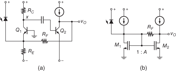
Figure 8.5 Current-mode TIA: simplified implementation examples.
Figure 8.5(b) shows a simplified version of the MOSFET circuit in [28]. Here, a current mirror with a small input transistor ![]() and a large output transistor
and a large output transistor ![]() amplifies the input current. This current amplifier has the low-frequency gain
amplifies the input current. This current amplifier has the low-frequency gain ![]() .
.
Some current-mode TIAs can operate from very low supply voltages, making them attractive for low-power applications [28]. However, current-mode TIAs tend to be noisier than voltage-mode TIAs.
8.3 TIA with Bootstrapped Photodetector
The effective photodetector capacitance ![]() seen by the TIA can be reduced by means of a circuit technique known as bootstrapping. Figure 8.6(a) shows the block diagram of a TIA with a bootstrapped photodetector [29–32]. Instead of biasing the photodetector at a fixed voltage above ground, it is biased at a fixed voltage above the TIA's input node. In the figure, the voltage buffer
seen by the TIA can be reduced by means of a circuit technique known as bootstrapping. Figure 8.6(a) shows the block diagram of a TIA with a bootstrapped photodetector [29–32]. Instead of biasing the photodetector at a fixed voltage above ground, it is biased at a fixed voltage above the TIA's input node. In the figure, the voltage buffer ![]() senses the TIA's input voltage, while loading this node as little as possible. Then, the reverse bias voltage
senses the TIA's input voltage, while loading this node as little as possible. Then, the reverse bias voltage ![]() is added to the buffer output voltage and the sum drives the photodetector. For an ideal bootstrap buffer with gain
is added to the buffer output voltage and the sum drives the photodetector. For an ideal bootstrap buffer with gain ![]() , the AC voltage across
, the AC voltage across ![]() becomes zero, suppressing any charging or discharging currents, effectively making
becomes zero, suppressing any charging or discharging currents, effectively making ![]() . For a bootstrap buffer with
. For a bootstrap buffer with ![]() , the residual photodetector capacitance becomes
, the residual photodetector capacitance becomes ![]() . Without bootstrapping,
. Without bootstrapping, ![]() , all of the detector capacitance is visible, as expected.
, all of the detector capacitance is visible, as expected.

Figure 8.6 TIA with bootstrapped photodetector: (a) block diagram and (b) a typical transistor-level implementation.
The bootstrap buffer is typically implemented with a source follower [33, 34] or an emitter follower [35]. An example circuit with a source follower is shown in Fig. 8.6(b). The source follower has the low-frequency gain  , where
 ![]() is the input resistance of the TIA (
is the input resistance of the TIA (![]() ) and
) and ![]() is the total load resistance at the source of
is the total load resistance at the source of ![]() (
(![]() , if the bias current source is ideal). This gain is always less than one, but approaches one for large values of
, if the bias current source is ideal). This gain is always less than one, but approaches one for large values of ![]() . (There are two mechanisms responsible for keeping the gain below one: the finite loop gain of the follower,
. (There are two mechanisms responsible for keeping the gain below one: the finite loop gain of the follower, ![]() , and the loading of the follower by the AC current
, and the loading of the follower by the AC current ![]() .)
.)
As shown in Fig. 8.6(b), a coupling capacitor ![]() together with a large biasing resistor
together with a large biasing resistor ![]() can be used to add the reverse bias voltage
can be used to add the reverse bias voltage ![]() to the buffer output voltage [34, 35]. Unfortunately, the gate–source voltage drop of the source follower reduces the reverse bias compared with the nonbootstrapped case and a higher supply voltage may be necessary. Alternatively, the follower can be DC coupled to the TIA input and the AC coupling capacitor is then added at the output of the buffer [33]. Noise injection from the bootstrap buffer is an important concern. A large bias resistor
to the buffer output voltage [34, 35]. Unfortunately, the gate–source voltage drop of the source follower reduces the reverse bias compared with the nonbootstrapped case and a higher supply voltage may be necessary. Alternatively, the follower can be DC coupled to the TIA input and the AC coupling capacitor is then added at the output of the buffer [33]. Noise injection from the bootstrap buffer is an important concern. A large bias resistor ![]() is needed to keep this noise low [34, 35].
is needed to keep this noise low [34, 35].
The bootstrap TIA in Fig. 8.6 comes in a number of variations. A separate bootstrap buffer ![]() in parallel with the voltage amplifier
in parallel with the voltage amplifier ![]() can be avoided, if the first stage of the voltage amplifier is a buffer stage. In this case, the bootstrap signal can simply be tapped off that buffer [29, 30]. In another variation, the drain of the source follower in Fig. 8.6(b) (or the collector of the emitter follower) is connected to the second input of a differential TIA, thus using the currents from both terminals of the photodetector [36, 37].
can be avoided, if the first stage of the voltage amplifier is a buffer stage. In this case, the bootstrap signal can simply be tapped off that buffer [29, 30]. In another variation, the drain of the source follower in Fig. 8.6(b) (or the collector of the emitter follower) is connected to the second input of a differential TIA, thus using the currents from both terminals of the photodetector [36, 37].
Another way of reducing the photodetector capacitance ![]() is to shunt it with a negative capacitance. A noninverting amplifier with gain
is to shunt it with a negative capacitance. A noninverting amplifier with gain ![]() and feedback capacitor
and feedback capacitor ![]() synthesizes the negative capacitance
synthesizes the negative capacitance ![]() at its input, which can be used for this purpose. This approach, which is sometimes known as a grounded-source bootstrap [31], results in the residual input capacitance
at its input, which can be used for this purpose. This approach, which is sometimes known as a grounded-source bootstrap [31], results in the residual input capacitance ![]() .
.
8.4 Burst-Mode TIA
The Burst-Mode Problem
How does a burst-mode TIA differ from the continuous-mode TIAs that we have discussed so far? A burst-mode TIA must be able to respond quickly to an input signal whose amplitude varies significantly from burst to burst. In passive optical networks (PON), the most common application for burst-mode TIAs, the amplitude variation (loud/soft ratio) at the central office (CO) can be up to ![]() (cf. Chapter 1). The burst-mode TIA adjusts to the amplitude of the individual bursts by means of a preamble. The preamble typically contains a 111…000… or a 101010… pattern or a combination of both [38] and its duration is between 10 and 1,000 bit periods, depending on the standard (e.g., BPON, GPON, EPON). The TIA must complete its adjustments in a fraction of this duration, because the main amplifier, the equalizer (if present), and the CDR require a settled TIA signal to make their adjustments.
(cf. Chapter 1). The burst-mode TIA adjusts to the amplitude of the individual bursts by means of a preamble. The preamble typically contains a 111…000… or a 101010… pattern or a combination of both [38] and its duration is between 10 and 1,000 bit periods, depending on the standard (e.g., BPON, GPON, EPON). The TIA must complete its adjustments in a fraction of this duration, because the main amplifier, the equalizer (if present), and the CDR require a settled TIA signal to make their adjustments.
Figure 8.7(a) illustrates a weak burst followed by a strong burst at the input of the TIA. (For clarity, the bursts are shown schematically as 5-bit 10101 patterns; in practice, the bursts are much longer.) Such a situation arises, for example, at the CO side of a PON system when a distant subscriber and a nearby subscriber transmit bursts in adjacent time slots (cf. Chapter 1). When received by a TIA with a fixed transimpedance, the distorted output signal shown in Fig. 8.7(b) is obtained. The horizontal dashed lines in Fig. 8.7(a) show the (fixed) input range of the TIA; outside of these lines, the TIA clips the signal. Clearly, such a TIA introduces severe pulse-width distortions that depend on the burst's strength and extinction ratio. (TIA overload effects, which are not considered in Fig. 8.7(b), make the situation worse.) In the case of a strong burst with a low extinction ratio (high zero-level signal), the burst may even be lost altogether.

Figure 8.7 Pulse-width distortions resulting from a TIA with fixed transimpedance: (a) input current and (b) output voltage.
These problems can be avoided with an adaptive TIA that adjusts the transimpedance from burst to burst such that the output signal does not get clipped or distorted. Visualize the dashed lines in Fig. 8.7(a) changing their vertical positions for every burst such that they are just outside of the burst's envelope. The correct decision threshold voltage, which minimizes pulse-width distortions and maximizes sensitivity, can then be determined based on the zero and one levels at the output of the TIA.
The length of the preamble and the coding scheme used for the payload impact the design choices for a burst-mode receiver. If the preamble is very long and the code has short runs (e.g., if the 8B/10B code is used), it is possible to use the same or similar circuits as for continuous-mode receivers [39]. The time constants for the gain control, offset control, and AC coupling simply must be chosen short enough such that the receiver settles within the preamble. Unfortunately, a PON system with such a long preamble has a poor bandwidth efficiency because a substantial fraction of the transmitted bits consist of preamble bits rather than payload bits. In contrast, if the preamble is short and the code has long runs (e.g., if the 64B/66B code is used), it is not possible to find a (single) time constant that simultaneously allows the receiver to settle within the preamble and that prevents the gain and offset control from drifting during long runs of zeros or ones. In this case, specialized burst-mode circuits are required.
To simultaneously achieve fast gain and offset control and high tolerance to long runs, burst-mode receivers make use of a reset signal that becomes active in between bursts. The reset signal erases the receiver's memory of the previous burst and prepares it for the next burst. The reset signal can be generated, for example, by tracing the burst's envelope or by counting the bits in the burst [40, 41]. We discuss this reset signal in more detail shortly.
Fast Gain Control
In Section 7.4, we discussed several ways of controlling the transimpedance in response to the received signal strength. The TIA with a nonlinear feedback or shunt network (cf. Figs 7.18 and 7.19), which compresses the dynamic range like a logarithmic amplifier, is a possible solution for burst-mode receivers [33]. It has the advantage of responding instantaneously and avoiding the need for a fast control loop. However, the nonlinear transfer function causes some pulse-width distortion [42] and strong bursts with low extinction ratio result in small output signals [43].
A linear TIA with a fast burst-by-burst gain control loop is shown in Fig. 8.8(a). The main difference to the continuous-mode AGC scheme shown in Fig. 7.13(a) is that the low-pass filter for measuring the signal swing has been replaced with a resetable peak detector. This peak detector responds to negative peaks and hence is also known as a bottom-level hold. The waveforms in Fig. 8.8(b) illustrate the operation for a strong burst followed by a weak burst. Before the first burst arrives, the peak detector is reset to the dark level of the TIA's output voltage, ![]() . Because this voltage is above
. Because this voltage is above ![]() , the gain-control switch opens and the higher of two transimpedance values is selected. When the strong burst arrives, the peak detector traces the lower edge of the envelope and as soon as it crosses below
, the gain-control switch opens and the higher of two transimpedance values is selected. When the strong burst arrives, the peak detector traces the lower edge of the envelope and as soon as it crosses below ![]() , the gain-control switch closes, thus reducing the transimpedance. For comparison, the response without gain control is also plotted (dashed line). At the end of the burst, the peak detector is reset and the gain-control switch opens in preparation for the next burst. When the weak burst arrives, the peak detector voltage never crosses below
, the gain-control switch closes, thus reducing the transimpedance. For comparison, the response without gain control is also plotted (dashed line). At the end of the burst, the peak detector is reset and the gain-control switch opens in preparation for the next burst. When the weak burst arrives, the peak detector voltage never crosses below ![]() and the transimpedance remains high. The relationship between the input swing and output swing for this burst-mode TIA is plotted in Fig. 8.8(c).
and the transimpedance remains high. The relationship between the input swing and output swing for this burst-mode TIA is plotted in Fig. 8.8(c).
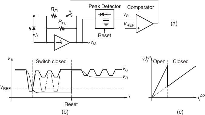
Figure 8.8 Burst-mode TIA with fast gain control: (a) block diagram, (b) waveforms, and (c) output swing versus input swing.
The circuit in Fig. 8.8(a) comes in a number of variations: More than two gain settings can be implemented with additional feedback resistors, switches, and comparators, resulting in a circuit similar to that in Fig. 7.14(b). (To keep Fig. 8.8(a) simple, the compensation capacitor ![]() is not shown.) Burst-mode TIAs with two gain settings [40, 44–47] and three gain settings [42] have been reported.
is not shown.) Burst-mode TIAs with two gain settings [40, 44–47] and three gain settings [42] have been reported.
Instead of discrete gain control (a.k.a. gain switching), continuous gain control, similar to that in Fig. 7.14(a), can be used [41, 43, 48]. Continuous gain control is of interest in applications that require good linearity and constant amplitude, such as in receivers with electronic dispersion compensation [48].
Instead of a variable feedback resistor, a variable shunt element at the input, similar to that in Fig. 7.16, can be used [49].
In a variation of the fast AGC loop in Fig. 8.8(a), the peak detector can be omitted if the subsequent comparator is designed with a large hysteresis [42, 47]. The idea is that once the signal crosses the threshold of the hysteresis comparator its output remains high (due to the hysteresis) and the switch remains closed, even when the signal returns to the dark level. The reset pulse must now be applied to the hysteresis comparator instead of the peak detector. (See Fig. 9.9 in Chapter 9 for a circuit example.)
In all burst-mode AGC schemes, gain switching after the preamble must be avoided to prevent corrupting the payload data. This issue may occur when the signal strength is just below the switching threshold during the preamble and a fluctuation in amplitude (or a noise peak) pushes it over the threshold during the payload. Freezing the gain at the end of the preamble resolves this issue [50].
Fast Offset and Threshold Control
Many burst-mode TIAs feature differential outputs that make the output signal more immune to coupled noise and that facilitate DC coupling to the subsequent burst-mode main amplifier. Burst-mode TIAs with differential outputs often include an offset control circuit that removes the output offset voltage [40, 42, 49]. Alternatively, the offset voltage can be removed at the input of the subsequent main amplifier [51]. Like gain control, offset control must be completed in a small fraction of the preamble's duration.
Adjusting the offset of a signal relative to a fixed decision threshold has the same effect as adjusting the decision threshold. Thus, in this context the terms automatic offset control (AOC) and automatic threshold control (ATC) are often used interchangeably.
A burst-mode TIA with differential outputs and fast threshold control is shown in Fig. 8.9(a) [41, 45, 46]. A single-ended burst-mode TIA is followed by a threshold voltage generator similar to the arrangement in Fig. 7.9, except that the slow ![]() low-pass filter has been replaced by two fast peak detectors and a voltage divider. One peak detector operates as a bottom-level hold and outputs
low-pass filter has been replaced by two fast peak detectors and a voltage divider. One peak detector operates as a bottom-level hold and outputs ![]() ; the other peak detector operates as a top-level hold and outputs
; the other peak detector operates as a top-level hold and outputs ![]() . The voltage divider produces the average voltage
. The voltage divider produces the average voltage ![]() . Figure 8.9(b) illustrates the output signal waveforms from the peak detectors for two sequential bursts with unequal amplitude. In between bursts, both detectors are reset to the dark level,
. Figure 8.9(b) illustrates the output signal waveforms from the peak detectors for two sequential bursts with unequal amplitude. In between bursts, both detectors are reset to the dark level, ![]() . When the burst arrives, the peak detectors trace the upper and the lower edge of the envelope and the midpoint between the two edges represents the threshold voltage
. When the burst arrives, the peak detectors trace the upper and the lower edge of the envelope and the midpoint between the two edges represents the threshold voltage ![]() . A subsequent differential stage amplifies the difference
. A subsequent differential stage amplifies the difference ![]() and produces the complementary output signals
and produces the complementary output signals ![]() and
and ![]() . The differential output voltage
. The differential output voltage ![]() swings symmetrically around the zero level and thus is offset free.
swings symmetrically around the zero level and thus is offset free.
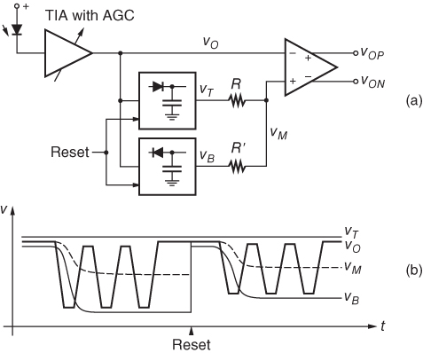
Figure 8.9 Burst-mode TIA with differential outputs and fast threshold control: (a) block diagram and (b) waveforms (simplified).
The timing of the reset signal is critical. Asserted in between bursts, it must be released only after the AGC process in the preceding TIA has settled (not shown in Fig. 8.9(b)) [40]. Otherwise, the bottom-level hold may pick up a transient, such as the first large negative peak in Fig. 8.8(b), resulting in the incorrect threshold voltage. Even in the absence of an AGC transient, the reset signal must be released only after the burst has started to correctly acquire the zero level [51]. If released too early, the top-level hold acquires the dark level, which is different from the zero level in the case of finite extinction.
The design of the peak detectors is critical. Their rise and fall times should be fast enough to track the envelope but not too fast to avoid tracking the noise in the received signal. Their droop (capacitor discharging) must be small enough to prevent the threshold voltage from drifting too much during long runs of zeros or ones [52]. Because the peak detectors in the AGC and the AOC/ATC circuits are both driven by the output of the single-ended TIA, they can be shared between these two functions [40, 41].
The circuit in Fig. 8.9(a) comes in a number of variations: To save chip area, the top-level hold can be replaced by a replica TIA with an open input [40] (cf. Fig. 7.8). However, the threshold is then based on the dark level instead of the zero level and the drift of the bottom-level hold due to the accumulation of noise peaks [51, 53] is no longer counterbalanced by a similar drift of the top-level hold.
In another variation, the threshold voltage ![]() is derived with an
is derived with an ![]() low-pass filter, just like in Fig. 7.9, thus getting rid of both peak detectors. But for this approach to work, the system must switch between two time constants: During the preamble, a fast time constant is selected to quickly acquire the average level of the burst, then during the payload, a slow time constant is selected to minimize drift of the threshold voltage during long runs of zeros or ones [45, 46, 54].
low-pass filter, just like in Fig. 7.9, thus getting rid of both peak detectors. But for this approach to work, the system must switch between two time constants: During the preamble, a fast time constant is selected to quickly acquire the average level of the burst, then during the payload, a slow time constant is selected to minimize drift of the threshold voltage during long runs of zeros or ones [45, 46, 54].
The circuit in Fig. 8.9(a) derives the offset-compensation voltage ![]() from the input signal, a method known as feedforward offset control. Alternatively,
from the input signal, a method known as feedforward offset control. Alternatively, ![]() can be derived from the output signals
can be derived from the output signals ![]() and
and ![]() [54], a method known as feedback offset control. Feedback offset control has the advantage of compensating offset errors in the whole receiver chain, but it is typically slower than feedforward offset control.
[54], a method known as feedback offset control. Feedback offset control has the advantage of compensating offset errors in the whole receiver chain, but it is typically slower than feedforward offset control.
Burst-Mode Penalty
In Section 4.2, we discussed the problem of acquiring the decision threshold based on a small number of preamble bits. The limited amount of averaging over the noisy zeros and ones results in a decision threshold that is necessarily corrupted by noise [52, 53, 55, 56]. The degree of corruption depends on the number of preamble bits that are averaged.
The burst-mode penalty resulting from this effect can be derived from Eq. (4.11) as [53]

where ![]() is the number of preamble bits used for threshold estimation and an equal number of zeros and ones is assumed. The expression in Eq. (8.13) is valid for a p–i–n receiver that acquires the zero and one levels by means of averaging. Similar expressions can be derived for an APD receiver (with unequal and non-Gaussian noise on the zeros and ones) [56] and for level acquisition with peak detectors (affected by drift due to the accumulation of noise peaks and discharge currents) [52, 53].
is the number of preamble bits used for threshold estimation and an equal number of zeros and ones is assumed. The expression in Eq. (8.13) is valid for a p–i–n receiver that acquires the zero and one levels by means of averaging. Similar expressions can be derived for an APD receiver (with unequal and non-Gaussian noise on the zeros and ones) [56] and for level acquisition with peak detectors (affected by drift due to the accumulation of noise peaks and discharge currents) [52, 53].
If the threshold is estimated from a single zero and a single one bit (![]() ) the power penalty according to Eq. (8.13) is
) the power penalty according to Eq. (8.13) is ![]() , which is rather large. Thus, a larger number of preamble bits is commonly used. In practice, burst-mode penalties of
, which is rather large. Thus, a larger number of preamble bits is commonly used. In practice, burst-mode penalties of ![]() [47] and
[47] and ![]() [51] (and about
[51] (and about ![]() in older burst-mode receivers [57, 58]) have been measured.
in older burst-mode receivers [57, 58]) have been measured.
For a continuous-mode receiver, the number of bits that are averaged to establish the decision threshold is very large (![]() ). In this case, Eq. (8.13) goes to one and the “burst-mode” penalty disappears.
). In this case, Eq. (8.13) goes to one and the “burst-mode” penalty disappears.
Chatter
There is one more peculiarity about burst-mode receivers. In between bursts there are extended periods of time when no optical signal is received. During these dead periods the transimpedance is usually set to its highest value and the decision threshold may be set close to zero in anticipation of a burst. Unfortunately, with these settings, the amplified TIA noise crosses the decision threshold randomly, generating a random bit sequence called chatter at the output of the receiver.
A brute force solution to this problem is to intentionally offset the decision threshold [57]. To suppress the chatter, the applied offset voltage must be larger than the expected peak noise voltage: ![]() (cf. Section 4.2). Moreover, the offset voltage must track the temperature dependence of the noise voltage [57]. However, an offset voltage of that magnitude degrades the sensitivity of the receiver by around
(cf. Section 4.2). Moreover, the offset voltage must track the temperature dependence of the noise voltage [57]. However, an offset voltage of that magnitude degrades the sensitivity of the receiver by around ![]() .
.
A better approach is to monitor the received signal strength to detect the presence or absence of a burst (activity detector) [51]. In the absence of a burst, the decision threshold is forced well above zero to avoid chatter. When a burst is detected, the ATC circuit acquires the optimum threshold voltage, thus avoiding the penalty associated with an intentional offset.
Peak Detectors
Given the importance of peak detectors in burst-mode circuits, a short discussion of their implementation is in order. Popular CMOS implementations of the top-level hold and the bottom-level hold are shown in Fig. 8.10 [41, 43, 45, 46, 51, 59].

Figure 8.10 CMOS implementations of (a) top-level hold and (b) bottom-level hold.
The top-level hold in Fig. 8.10(a) operates as follows: If the input voltage ![]() exceeds the output voltage
exceeds the output voltage ![]() (the peak value acquired thus far), the output of the amplifier goes high. In response, the gate-drain connected MOSFET
(the peak value acquired thus far), the output of the amplifier goes high. In response, the gate-drain connected MOSFET ![]() , which acts as a diode, turns on and charges capacitor
, which acts as a diode, turns on and charges capacitor ![]() . The voltage of the capacitor is buffered and level-shifted by the source follower
. The voltage of the capacitor is buffered and level-shifted by the source follower ![]() and fed back to the amplifier input. As soon as the capacitor is charged enough for
and fed back to the amplifier input. As soon as the capacitor is charged enough for ![]() to match
to match ![]() , the amplifier turns diode
, the amplifier turns diode ![]() off and the charging stops. Thanks to the feedback loop through the amplifier, the voltage drops across the diode
off and the charging stops. Thanks to the feedback loop through the amplifier, the voltage drops across the diode ![]() and the source follower
and the source follower ![]() are suppressed. To reset the peak detector, capacitor
are suppressed. To reset the peak detector, capacitor ![]() is discharged with
is discharged with ![]() .
.
The bottom-level hold in Fig. 8.10(b) operates in the same way, except that the polarity of diode ![]() is reversed to acquire the bottom level.
is reversed to acquire the bottom level.
Some peak detector circuits merge the diode function with the amplifier function. In fact, an amplifier that can only source (for a top-level hold) or only sink (for a bottom-level hold) current may be faster than a regular amplifier followed by a diode. Amplifiers with an open collector [50], open drain [60], or an unbiased emitter follower [61] can be used for this purpose.
A potential issue with peak detectors is that they may overshoot (for a top-level hold) or undershoot (for a bottom-level hold) their target value [50, 60]. This overshoot (or undershoot) is caused by the delay through the amplifier, ![]() , and
, and ![]() , which results in a late turn off of the current that charges
, which results in a late turn off of the current that charges ![]() . One way to compensate for overshoot (undershoot) is to artificially increase (decrease) the voltage that is fed back to the amplifier [50].
. One way to compensate for overshoot (undershoot) is to artificially increase (decrease) the voltage that is fed back to the amplifier [50].
8.5 Analog Receiver TIA
Optical fiber communication also has a significant impact on analog RF and microwave applications that traditionally have relied on coaxial cable. The low loss of optical fiber permits the elimination of many RF boosting amplifiers. The elimination of these amplifiers, in turn, results in a link with lower noise and distortion.
A typical application of this type is the hybrid fiber-coax (HFC) network used to distribute CATV signals from the head end to the neighborhood through optical fiber (cf. Chapter 1). Another example is the distribution of CATV signals over a PON by means of a dedicated wavelength (video overlay) [62]. Analog optical links are also used to connect wireless base stations with remote antennas. This application is referred to as microwave photonics [63] or radio over fiber (RoF) [64].
In contrast to digital receivers, analog receivers must be highly linear to keep distortions in the fragile analog signals (e.g., QAM or AM-VSB signals) to a minimum. The linearity of CATV receivers is specified in terms of the composite second order (CSO) distortion and the composite triple beat (CTB) distortion. For these and other nonlinearity measures, see Appendix D.
In addition, analog receivers require a much higher ratio of signal to noise than digital receivers. The noise performance of CATV receivers is specified in terms of the carrier-to-noise ratio (CNR), the passband equivalent of the signal-to-noise ratio (SNR) (cf. Section 4.3). The noise performance of microwave photonic links is specified in terms of the noise figure [63].
Low-Impedance Front-End
A simple implementation of an analog receiver is shown in Fig. 8.11(a). It consists of a low-impedance front-end followed by a linear low-noise amplifier [65]. Typically, the front-end impedance and the amplifier input impedance are ![]() (or
(or ![]() in CATV systems) such that standard cables and connectors can be used.
in CATV systems) such that standard cables and connectors can be used.

Figure 8.11 Receivers for analog signals: (a) low-impedance front-end and (b) front-end with matching network.
To achieve high linearity, the p–i–n photodetector must be operated below its saturation current (cf. Section 3.1). A beam splitter, multiple photodetectors, and a power combiner can be used to increase the effective saturation current of the photodetector, if necessary [66].
Amplifiers for CATV applications typically consist of a balun, that is, a transformer that converts the single-ended input signal to a balanced differential signal, followed by a differential amplifier with good symmetry (a push–pull amplifier), and another balun for converting the differential signal back to a single-ended output signal [67, 68]. Owing to its symmetry, this topology exhibits low even-order (in particular, low second-order) distortions.
Noise Matching
As we know, the low-impedance front-end in Fig. 8.11(a) is rather noisy. A transformer that matches the low input impedance of the amplifier to the higher impedance of the photodetector, as shown in Fig. 8.11(b), can be used to improve the noise performance [69]. The example shown in the figure uses an autotransformer with a turns ratio of 4:1 to transform the 75-![]() input impedance of the CATV amplifier up to
input impedance of the CATV amplifier up to ![]() (16:1 impedance ratio). Such a transformer can be constructed, for example, by winding six turns from the input to the center tap (output) and two turns from the center tap to the ground on a ferrite core. This matching technique eliminates the load resistor to ground and the noise associated with it. Furthermore, because the transformer has a current gain of
(16:1 impedance ratio). Such a transformer can be constructed, for example, by winding six turns from the input to the center tap (output) and two turns from the center tap to the ground on a ferrite core. This matching technique eliminates the load resistor to ground and the noise associated with it. Furthermore, because the transformer has a current gain of ![]() , the input-referred noise current of the amplifier is attenuated by the same factor
, the input-referred noise current of the amplifier is attenuated by the same factor ![]() (corresponding to
(corresponding to ![]() ) when referred back to the photodetector.
) when referred back to the photodetector.
While the transformer helps with the noise, it also reduces the bandwidth. For example, a photodetector with a 0.2-pF capacitance loaded by the 1.2-![]() resistance seen through the transformer limits the bandwidth to about
resistance seen through the transformer limits the bandwidth to about ![]() , which is not sufficient for most CATV applications (CATV signals occupy the frequency band from
, which is not sufficient for most CATV applications (CATV signals occupy the frequency band from ![]() up to
up to ![]() ). However, adding a small series inductor
). However, adding a small series inductor ![]() (see Fig. 8.11(b)) can increase the bandwidth to the desired value (cf. Section 7.7) and even provide some uptilt in the frequency response, if desired [69].
(see Fig. 8.11(b)) can increase the bandwidth to the desired value (cf. Section 7.7) and even provide some uptilt in the frequency response, if desired [69].
More generally, the input-referred noise of analog receivers can be shaped and reduced by placing a noise matching network between the photodetector and the TIA [69–71]. We discussed this technique in Section 6.5. Compared to digital receivers, the higher low-frequency cutoff typical for analog receivers (e.g., ![]() ) permits more flexibility in the design of the noise matching network.
) permits more flexibility in the design of the noise matching network.
Balanced Photodetector
In Section 4.4, we discussed the noise of analog receivers and found that it is composed of circuit noise, shot noise, and relative intensity noise (RIN). While noise matching can reduce the circuit noise, it cannot help with the shot and RIN noise.
To suppress the RIN noise, which originates from the laser in the transmitter, a receiver with a balanced detector can be used [63]. For examples of receivers with balanced detectors, see Section 3.5. In this scheme, the transmitter generates complementary optical signals with a Mach–Zehnder modulator, which are transmitted through two separate fibers. At the receiver, the balanced photodetector subtracts the two optical inputs, recovering the modulated signal but rejecting the common-mode RIN noise. With this method photonic microwave links with noise figures below ![]() up to
up to ![]() have been realized [63].
have been realized [63].
Shunt-Feedback TIA
Shunt-feedback TIAs can achieve better noise performance than low-impedance front-ends (cf. Chapter 6). Figure 8.12(a) shows an analog receiver with a single-ended shunt-feedback TIA [72]. The photodetector is AC coupled to the TIA input. The bias resistor ![]() sets the reverse voltage of the photodetector to
sets the reverse voltage of the photodetector to ![]() , where
, where ![]() is the supply voltage,
is the supply voltage, ![]() is the responsivity of the photodetector, and
is the responsivity of the photodetector, and ![]() is the average received optical power, usually between
is the average received optical power, usually between ![]() and
and ![]() for CATV applications. Alternatively, an RF choke or a combination of RF choke and resistor can be used to reduce the voltage drop and noise of the bias network. In any case, the impedance of the bias network must be high compared with the input resistance of the TIA in the frequency band of interest, such that almost all AC current from the detector flows through the coupling capacitor into the TIA. Similar to the DC input current control circuits discussed in Section 7.3, the bias network removes the DC component of the photodetector current, leaving only the AC current for the TIA. For CATV applications, in which the minimum frequency is
for CATV applications. Alternatively, an RF choke or a combination of RF choke and resistor can be used to reduce the voltage drop and noise of the bias network. In any case, the impedance of the bias network must be high compared with the input resistance of the TIA in the frequency band of interest, such that almost all AC current from the detector flows through the coupling capacitor into the TIA. Similar to the DC input current control circuits discussed in Section 7.3, the bias network removes the DC component of the photodetector current, leaving only the AC current for the TIA. For CATV applications, in which the minimum frequency is ![]() , a relatively small coupling capacitor (1 to
, a relatively small coupling capacitor (1 to ![]() ) is sufficient.
) is sufficient.
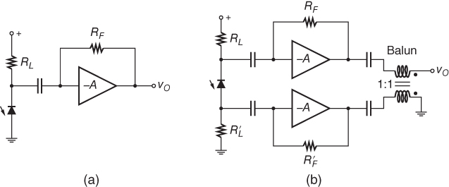
Figure 8.12 Shunt-feedback TIAs for analog receivers: (a) single ended topology and (b) pseudo-differential topology with differentially coupled photodetector.
To achieve the necessary high linearity with a single-ended TIA, the voltage amplifier must operate at a high supply voltage and a large quiescent current (e.g., ![]() and
and ![]() for CATV applications) such that the signal excursions are only a small percentage of the operating point [72, 73]. Moreover, to keep the output signal within the linear operating region of the amplifier, the TIA must have an adaptive transimpedance (variable
for CATV applications) such that the signal excursions are only a small percentage of the operating point [72, 73]. Moreover, to keep the output signal within the linear operating region of the amplifier, the TIA must have an adaptive transimpedance (variable ![]() ) [72] (cf. Section 7.4).
) [72] (cf. Section 7.4).
The large power dissipation that results from the high supply voltage and quiescent current makes copackaging an analog TIA with a photodetector challenging [73]. Therefore, analog TIA circuits that dissipate less power while maintaining high linearity are needed.
Differential Shunt-Feedback TIA
TIAs with differential inputs and outputs depend less on transistor linearity because the symmetry of the differential topology ensures low even-order distortions. The resulting lower operating-point voltages and currents lead to a lower power dissipation.
The pseudo-differential TIA shown in Fig. 8.12(b) relies on good matching between its two halves to minimize the even-order distortions. (A slight imbalance may be introduced on purpose to compensate for the photodetector nonlinearity [69].) A balun can be used to connect the single-ended photodetector to the differential TIA inputs, but the preferred method is to take complementary current signals from the two terminals of the photodetector [67, 69, 71], as shown in Fig. 8.12(b). This arrangement avoids the bandwidth limitation inherent with a balun. The bias resistors ![]() and
and ![]() , together with the average photodetector current, set the reverse voltage of the photodetector. Again, RF chokes can be used as part of the bias network to reduce voltage drops and noise [71].
, together with the average photodetector current, set the reverse voltage of the photodetector. Again, RF chokes can be used as part of the bias network to reduce voltage drops and noise [71].
To obtain well balanced input signals, the parasitic capacitances of the photodetector and the interconnects must be similarly well balanced. Interestingly, the pseudo-differential TIA is more resilient to an input-capacitance imbalance than the regular differential TIA. Whereas both topologies have the same differential input resistances, ![]() , the pseudo-differential TIA has a lower common-mode input resistance,
, the pseudo-differential TIA has a lower common-mode input resistance, ![]() , that the regular differential TIA,
, that the regular differential TIA, ![]() . This lower common-mode input resistance helps to suppress the AC common-mode voltage that otherwise would throw the voltage amplifier off balance.
. This lower common-mode input resistance helps to suppress the AC common-mode voltage that otherwise would throw the voltage amplifier off balance.
Differential coupling of the photodetector to the TIA eliminates the balun at the input, but another balun is still needed to convert the differential output signals back to a single-ended output signal (cf. Fig. 8.12(b)). In a current-mode implementation, where the amplifier output signals are in the form of currents, the current subtraction can be done by means of Kirchhoff's current law, avoiding the balun necessary for a voltage subtraction [74].
Distortion Cancellation
Another technique for simultaneously obtaining high linearity and low power dissipation is distortion cancellation. The idea is to follow a first stage, which is slightly nonlinear, by a second stage that attempts to undo the nonlinearity of the first one.
For example, in [73] a cascoded common-source stage is followed by a common-drain stage that approximately cancels the distortions of the first one. This linearized voltage amplifier forms the core of a single-ended shunt-feedback TIA. Careful tuning of the bias currents in the two stages results in inversely related nonlinearities and an overall linear response without the need for large operating-point voltages and currents.
Another example of distortion cancellation is the nonlinear active-feedback TIA followed by an inversely related nonlinear post amplifier that we mentioned in Section 8.1 [19, 20].
8.6 Summary
Capacitive feedback eliminates the noise generated by the feedback resistor in a conventional shunt-feedback TIA. However, simply replacing the feedback resistor with a capacitor turns the TIA into an integrator. One way to resolve this issue is to follow the integrator with a differentiator; another way is to use a capacitive current divider as the feedback element.
Optical feedback also has the potential of lowering the noise, but unlike resistive feedback it cannot be integrated in a standard circuit technology.
Active feedback (feedback through a transistor) comes in several forms: common source, common drain, or common gate for a FET and common emitter, common collector, or common base for a BJT. Active feedback also has the potential of lowering the noise, but its linearity is inferior to that of resistive feedback.
Current-mode TIAs promise gain-bandwidth independence, but when taking all parasitic capacitances into account, their performance is often not much different from that of voltage-mode TIAs.
Bootstrapping makes the effective photodetector capacitance appear smaller. In one implementation, the photodetector is driven such that the AC voltage drop across the detector becomes small. In another implementation, a negative capacitance is synthesized and applied in parallel to the detector.
Burst-mode TIAs, used for example in receivers for passive optical networks (PON), feature fast gain control and fast offset (or threshold) control to deal with bursty signals that have large burst-to-burst amplitude variations. To quickly acquire the burst amplitude, peak detectors, which are reset in between bursts, are commonly used. The gain and offset of burst-mode TIAs are set on a burst-by-burst basis.
Analog TIAs, used for example in receivers for hybrid fiber-coax (HFC) networks and microwave photonic links, feature high linearity and low noise to minimize signal distortions. Noise matching with transformers and inductors, symmetric (push–pull) designs to minimize even-order distortions, and distortion cancellation with inversely related nonlinearities are some of the techniques used.
Problems
-
8.1 Active-Feedback TIA with Common-Source Feedback Device. (a) Calculate the transimpedance
 of the active-feedback TIA shown in Fig. 8.3(a). Assume a single-pole model (with time constant
  ) for the voltage amplifier, define the total input capacitance as
  , and neglect
  and
and  of
of  . (b) What time constant
  is needed to obtain a Butterworth response? (c) What is the 3-dB bandwidth of the TIA given a Butterworth response? (d) Does the transimpedance limit Eq. (6.14) apply to this TIA? (e) Calculate the input-referred noise current PSD of this active-feedback TIA, taking the noise contributions from the feedback FET and the front-end FET into account. (f) Repeat the noise calculation for a TIA with a BJT front-end and feedback through a common-emitter BJT.
 -
8.2 Active-Feedback TIA with Common-Drain Feedback Device. (a) Calculate the transimpedance
 of the active-feedback TIA shown in Fig. 8.3(b). Assume a single-pole model (with time constant
  ) for the voltage amplifier, define the total input capacitance as
  , and neglect
  and
and  of
of  . (b) Does the transimpedance limit Eq. (6.14) apply to this TIA? (c) Calculate the input-referred noise current PSD of this active-feedback TIA, taking the noise contributions from the feedback FET and the front-end FET into account.
 -
8.3 Current-Mode TIA. (a) Calculate the transimpedance
 of the current-mode TIA shown in Fig. 8.4. Assume a single-pole model (with time constant
  ) for the current amplifier,
  , and
, and  . What is the 3-dB bandwidth of the TIA given a Butterworth response and
  ? (b) Repeat (a), but now assume
  , and
, and  . What is the 3-dB bandwidth of the TIA given a Butterworth response and
  ? Derive the transimpedance limit.
References
- 1 C. Ciofi, F. Crupi, C. Pace, G. Scandurra, and M. Patanè. A new circuit topology for the realization of very low-noise wide-bandwidth transimpedance amplifier. IEEE Trans. Instrum. Meas., IM-56(5):1626–1631, 2007.
- 2 G. Ferrari, F. Gozzini, A. Molari, and M. Sampietro. Transimpedance amplifier for high sensitivity current measurements on nanodevices. IEEE J. Solid-State Circuits, SC-44(5):1609–1616, 2009.
- 3 B. Razavi. A 622Mb/s, 4.5pA/
 CMOS transimpedance amplifier. In ISSCC Digest of Technical Papers, pages 162–163, February 2000.
 - 4 S. Shahdoost, B. Bozorgzadeh, A. Medi, and N. Saniei. Low-noise transimpedance amplifier design procedure for optical communications. In IEEE Austrian Workshop on Microelectronics (Austrochip), pages 1–5, October 2014.
- 5 J. Salvia, P. Lajevardi, M. Hekmat, and B. Murmann. A 56MΩ CMOS TIA for MEMS applications. In Proceedings of IEEE Custom Integrated Circuits Conference, pages 199–202, September 2009.
- 6 A. E. Stevens. An Integrate-and-Dump Receiver for Fiber Optic Networks. PhD thesis, Columbia University, New York, 1995.
- 7 B. L. Kasper. Receiver using optical feedback. U.S. Patent No. 4,744,105, May 1988.
- 8 B. L. Kasper, A. R. McCormick, C. A. Burrus Jr., and J. R. Talman. An optical-feedback transimpedance receiver for high sensitivity and wide dynamic range at low bit rates. J. Lightwave Technol., LT-6(2):329–338, 1988.
- 9 G. F. Williams. Nonintegrating receiver. U.S. Patent No. 4,540,952, September 1985.
- 10 E. Braß, U. Hilleringmann, and K. Schumacher. System integration of optical devices and analog CMOS amplifiers. IEEE J. Solid-State Circuits, SC-29(8):1006–1010, 1994.
- 11 C. Rooman, D. Coppée, and M. Kuijk. Asynchronous 250-Mb/s optical receivers with integrated detector in standard CMOS technology for optocoupler applications. IEEE J. Solid-State Circuits, SC-35(7):953–958, 2000.
- 12 S. B. Baker and C. Toumazou. Low noise CMOS common gate optical preamplifier using active feedback. Electron. Lett., 34(23):2235–2237, 1998.
- 13 H. M. Lavasani, W. Pan, B. Harrington, R. Abdolvand, and F. Ayazi. A 76 dB
 1.7 GHz 0.18
  m CMOS tunable TIA using broadband current pre-amplifier for high frequency lateral MEMS oscillators. IEEE J. Solid-State Circuits, SC-46(1):224–235, 2011.
 - 14 Z. Lu, K. S. Yeo, W. M. Lim, M. A. Do, and C. C. Boon. Design of a CMOS broadband transimpedance amplifier with active feedback. IEEE Trans. Very Large Scale Integr. Syst., VLSI-18(3):461–472, 2010.
- 15 J. S. Yun, M. Seo, B. Choi, J. Han, Y. Eo, and S. M. Park. A 4Gb/s current-mode optical transceiver in 0.18
 m CMOS. In ISSCC Digest of Technical Papers, pages 102–103, February 2009.
 - 16 S. Andersson, C. Svensson, and O. Drugge. Wideband LNA for a multistandard wireless receiver in 0.18
 m CMOS. In Proceedings of European Solid-State Circuits Conference, pages 655–658, September 2003.
 - 17 J. Borremans, P. Wambacq, C. Soens, Y. Rolain, and M. Kuijk. Low-area active-feedback low-noise amplifier design in scaled digital CMOS. IEEE J. Solid-State Circuits, SC-43(11):2422–2433, 2008.
- 18 B. Razavi. RF Microelectronics. Prentice-Hall, Inc., Upper Saddle River, NJ, 1998.
- 19 A. Kopa and A. B. Apsel. 124dB Hz2/3 dynamic range transimpedance amplifier for electronic-photonic channelizer. In Proceedings of IEEE International Symposium on Circuits and Systems, pages 189–192, Seattle, WA, May 2008.
- 20 A. Kopa and A. B. Apsel. Common-emitter feedback transimpedance amplifier for analog optical receivers. In Proceedings of IEEE International Symposium on Circuits and Systems, pages 5479–5482, Island of Kos, May 2006.
- 21 S. Galal and B. Razavi. 10-Gb/s limiting amplifier and laser/modulator driver in 0.18-
 CMOS technology. IEEE J. Solid-State Circuits, SC-38(12):2138–2146, 2003.
 - 22 E. Säckinger. Broadband Circuits for Optical Fiber Communication. John Wiley &Sons, Inc., Hoboken, NJ, 2005.
- 23 K.-Y. Toh, R. G. Meyer, D. C. Soo, G. M. Chin, and A. M. Voshchenkov. Wide-band, low-noise, matched-impedance amplifiers in submicrometer MOS technology. IEEE J. Solid-State Circuits, SC-22(6):1031–1040, 1987.
- 24 B. Wilson and J. D. Drew. Novel transimpedance amplifier formulation exhibiting gain-bandwidth independence. In IEEE International Symposium on Circuits and Systems Proceedings, pages 169–172, 1997.
- 25 B. Wilson and J. D. Drew. High-performance transimpedance formulation for MESFET- and HBT-based monolithic microwave integrated circuits. IEE Proc. Circuits Devices Syst., 145(6):429–436, 1998.
- 26 E. Säckinger. The transimpedance limit. IEEE Trans. Circuits Syst. I, CASI-57(8):1848–1856, 2010.
- 27 A. S. Sedra and G. W. Roberts. Current conveyor theory and practice. In C. Toumazou, F. J. Lidgey, and D. G. Haigh, editors, Analogue IC Design: The Current-Mode Approach, pages 93–126. Institution of Engineering and Technology (IET), London, UK, 1990.
- 28 K. Phang and D. A. Johns. A 1V 1mW CMOS front-end with on-chip dynamic gate biasing for 75Mb/s optical receiver. In ISSCC Digest of Technical Papers, pages 218–219, February 2001.
- 29 M. Abraham. Design of Butterworth-type transimpedance and bootstrap-transimpedance preamplifiers for fiber-optic receivers. IEEE Trans. Circuits Syst., CAS-29(6):375–382, 1982.
- 30 M. Abraham. Bootstrap-transimpedance preamplifier for a fiber optic receiver. U.S. Patent No. 4,535,233, August 1985.
- 31 C. Hoyle and A. Peyton. Bootstrapping techniques to improve the bandwidth of transimpedance amplifiers. In IEE Colloquium on Analog Signal Processing, pages 7/1–7/6, Oxford, UK, October 1998.
- 32 C. Hoyle and A. Peyton. Shunt bootstrapping technique to improve bandwidth of transimpedance amplifiers. Electron. Lett., 35(5):369–370, 1999.
- 33 S. Brigati, P. Colombara, L. D'Ascoli, U. Gatti, T. Kerekes, and P. Malcovati. A SiGe BiCMOS burst-mode 155-Mb/s receiver for PON. IEEE J. Solid-State Circuits, SC-37(7):887–894, 2002.
- 34 C.-M. Tsai. A 20mW 85dBΩ 1.25Gb/s CMOS transimpedance amplifier with photodiode capacitance cancellation. In Symposium on VLSI Circuits Digest of Technical Papers, pages 408–409, June 2004.
- 35 A. Maxim. A 54 dBΩ + 42 dB 10 Gb/s SiGe transimpedance-limiting amplifier using bootstrap photodiode capacitance neutralization and vertical threshold adjustment. IEEE J. Solid-State Circuits, SC-42(9):1851–1864, September 2007. This paper may contain falsified information, see the June 2008 issue.
- 36 C.-M. Tsai. A 40 mW 3 Gb/s self-compensated differential transimpedance amplifier with enlarged input capacitance tolerance in 0.18
 m CMOS technology. IEEE J. Solid-State Circuits, SC-44(10):2671–2677, 2009.
 - 37 C.-M. Tsai and L.-R. Huang. A 21mW 2.5Gb/s 15kΩ self-compensated differential transimpedance amplifier. In ISSCC Digest of Technical Papers, pages 234–235, February 2005.
- 38 X.-Z. Qiu, P. Ossieur, J. Bauwelinck, Y. Yi, D. Verhulst, J. Vandewege, B. De Vos, and P. Solina. Development of GPON upstream physical-media-dependent prototypes. J. Lightwave Technol., LT-22(11):2498–2508, 2004.
- 39 K. Hara, S. Kimura, H. Nakamura, N. Yoshimoto, and H. Hadama. New AC-coupled burst-mode optical receiver using transient-phenomena cancellation techniques for 10 Gbit/s-class high-speed TDM-PON systems. J. Lightwave Technol., LT-28(19):2775–2782, 2010.
- 40 Q. Le, S.-G. Lee, H.-Y. Kang, and S.-H. Chai. A CMOS burst-mode TIA with step AGC and selective internally created reset for 1.25Gb/s EPON. In ISSCC Digest of Technical Papers, pages 50–51, February 2007.
- 41 Q. Le, S.-G. Lee, Y.-H. Oh, H.-Y. Kang, and T.-H. Yoo. A burst-mode receiver for 1.25-Gb/s Ethernet PON with AGC and internally created reset signal. IEEE J. Solid-State Circuits, SC-39(12):2379–2388, 2004.
- 42 M. Nakamura, Y. Imai, Y. Umeda, J. Endo, and Y. Akatsu. 1.25-Gb/s burst-mode receiver ICs with quick response for PON systems. IEEE J. Solid-State Circuits, SC-40(12):2680–2688, 2005.
- 43 S. Yamashita, S. Ide, K. Mori, A. Hayakawa, N. Ueno, and K. Tanaka. Novel cell-AGC technique for burst-mode CMOS preamplifier with wide dynamic range and high sensitivity for ATM-PON system. IEEE J. Solid-State Circuits, SC-37(7):881–886, 2002.
- 44 W.-Z. Chen and R.-M. Gan. 1.8V variable gain transimpedance amplifiers with constant damping factor for burst-mode optical receiver. In IEEE Radio Frequency Integrated Circuits (RFIC) Symposium, pages 691–694, Long Beach, CA, June 2005.
- 45 W.-Z. Chen and R.-M. Gan. A single chip 2.5 Gbps CMOS burst mode optical receiver. In Symposium on VLSI Circuits Digest of Technical Papers, pages 120–121, June 2006.
- 46 W.-Z. Chen, R.-M. Gan, and S.-H. Huang. A single-chip 2.5-Gb/s CMOS burst-mode optical receiver. IEEE Trans.Circuits Syst. I, CASI-56(10):2325–2331, 2009.
- 47 S. Nishihara, S. Kimura, T. Yoshida, M. Nakamura, J. Terada, K. Nishimura, K. Kishine, K. Kato, Y. Ohtomo, N. Yoshimoto, T. Imai, and M. Tsubokawa. A burst-mode 3R receiver for 10-Gbit/s PON systems with high sensitivity, wide dynamic range, and fast response. J. Lightwave Technol., LT-26(1):99–107, 2008.
- 48 P. Ossieur, N. A. Quadir, S. Porto, C. Antony, W. Han, M. Rensing, P. O'Brien, and P. D. Townsend. A 10 Gb/s linear burst-mode receiver in 0.25
 SiGe:C BiCMOS. IEEE J. Solid-State Circuits, SC-48(2):381–390, 2013.
 - 49 K. Nishimura, H. Kimura, M. Watanabe, T. Nagai, K. Nojima, K. Gomyo, M. Takata, M. Iwamoto, and H. Asano. A 1.25-Gb/s CMOS burst-mode optical transceiver for Ethernet PON system. IEEE J. Solid-State Circuits, SC-40(4):1027–1034, 2005.
- 50 T. De Ridder, P. Ossieur, B. Baekelandt, C. Mélange, J. Bauwelinck, C. Ford, X.-Z. Qui, and J. Vandewege. A 2.7V 9.8Gb/s burst-mode TIA with fast automatic gain locking and coarse threshold extraction. In ISSCC Digest of Technical Papers, pages 220–221, February 2008.
- 51 P. Ossieur, D. Verhulst, Y. Martens, W. Chen, J. Bauwelinck, X.-Z. Qui, and J. Vandewege. A 1.25-Gb/s burst-mode receiver for GPON applications. IEEE J. Solid-State Circuits, SC-40(5):1180–1189, 2005.
- 52 C. Su, L.-K. Chen, and K.-W. Cheung. Theory of burst-mode receiver and its applications in optical multiaccess networks. J. Lightwave Technol., LT-15(4):590–606, 1997.
- 53 P. Menéndez-Valdés. Performance of optical direct receivers using noise corrupted decision threshold. J. Lightwave Technol., LT-13(11):2202–2214, 1995.
- 54 R. Weber, M. Levy, and R. Dvir. Transimpedance (TIA) circuit usable for burst mode communications. U.S. Patent No. 7,583,904 B2, September 2009.
- 55 C. A. Eldering. Theoretical determination of sensitivity penalty for burst mode fiber optic receivers. J. Lightwave Technol., LT-11(12):2145–2149, 1993.
- 56 P. Ossieur, X.-Z. Qiu, J. Bauwelinck, and J. Vandewege. Sensitivity penalty calculation for burst-mode receivers using avalanche photodiodes. J. Lightwave Technol., LT-21(11):2565–2575, 2003.
- 57 Y. Ota and R. G. Swartz. Burst-mode compatible optical receiver with a large dynamic range. J. Lightwave Technol., LT-8(12):1897–1903, 1990.
- 58 Y. Ota, R. G. Swartz, and V. D. Archer III. DC-1Gb/s burst-mode compatible receiver for optical bus applications. J. Lightwave Technol., LT-10(2):244–249, 1992.
- 59 M. Nakamura, N. Ishihara, and Y. Akazawa. A 156-Mb/s CMOS optical receiver for burst-mode transmission. IEEE J. Solid-State Circuits, SC-33(8):1179–1187, 1998.
- 60 H.-L. Chu and S.-I. Liu. A 10Gb/s burst-mode transimpedance amplifier in
 CMOS. In IEEE Asian Solid-State Circuits Conference (ASSCC), pages 400–403, November 2007.
 - 61 Y. Ota, R. G. Swartz, V. D. Archer III, S. K. Korotky, M. Banu, and A. E. Dunlop. High-speed, burst-mode, packet-capable optical receiver and instantaneous clock recovery for optical bus operation. J. Lightwave Technol., LT-12(2):325–331, 1994.
- 62 F. Effenberger. PONs: state of the art and standardized. In I. P. Kaminow, T. Li, and A. E. Willner, editors, Optical Fiber Telecommunications VIB, pages 891–926. Academic Press, 2013.
- 63 C. H. Cox III and E. I. Ackerman. Recent advances in high-frequency (
 10GHz) microwave photonic links. In I. P. Kaminow, T. Li, and A. E. Willner, editors, Optical Fiber Telecommunications VIB, pages 853–872. Academic Press, 2013.
 - 64 G.-K. Chang, Y.-T. Hsueh, and S.-H. Fan. Advances in 1--100GHz microwave photonics: all-band optical wireless access networks using radio over fiber technologies. In I. P. Kaminow, T. Li, and A. E. Willner, editors, Optical Fiber Telecommunications VIB, pages 873–890. Academic Press, 2013.
- 65 J. Chen, F. Saibi, E. Säckinger, J. Othmer, M.-L. (Mark) Yu, F. Yang, J. Lin, T. Huang, T.-P. Liu, and K. Azadet. A multi-carrier QAM transceiver for ultra-wideband optical communication. IEEE J. Solid-State Circuits, SC-41(8):1876–1893, 2006.
- 66 S. Itakura, K. Sakai, T. Nagatsuka, E. Ishimura, M. Nakaji, H. Otsuka, K. Mori, and Y. Hirano. High-current backside-illuminated photodiode array module for optical analog links. J. Lightwave Technol., LT-28(6):965–971, 2010.
- 67 B. L. Kasper. Lightwave receiver having differential input. U.S. Patent No. 5,013,903, May 1991.
- 68 Philips Semiconductors. A hybrid wideband amplifier module for digital CATV networks with the BGD902. Philips Semiconductors, Application Note AN98109, February 1999.
- 69 H. A. Blauvelt, I. Ury, D. B. Huff, and H. L. Loboda. Broadband optical receiver with passive tuning network. U.S. Patent No. 5,179,461, January 1993.
- 70 F. R. Little Jr., H. A. Kruse, and J. Megna. Push-pull optical receiver. U.S. Patent No. 5,239,402, August 1993.
- 71 J. Skrobko. Push-pull optical receiver with cascode amplifiers. U.S. Patent No. 5,347,389, September 1994.
- 72 H. A. Kruse. Fiber optic transimpedance receiver. U.S. Patent No. 4,998,012, March 1991.
- 73 B. L. Kasper and E. M. Peral. Distortion cancellation in a transimpedance amplifier circuit. U.S. Patent Application No. 2007/0003291 A1, January 2007.
- 74 R. A. Gosser and E. P. Jordan. Low-distortion transimpedance amplifier structures and methods. U.S. Patent No. 6,529,078 B1, March 2003.