Chapter 3
Photodetectors
The first element of an optical receiver is the photodetector. The characteristics of this device have a significant impact on the receiver's performance. To achieve a good receiver sensitivity, the photodetector must have a large response to the received optical signal, have a bandwidth that is sufficient for the incoming signal, and generate as little noise as possible.
We start with the three most common photodetectors: the p–i–n photodetector, the avalanche photodetector (APD), and the optically preamplified p–i–n detector, discussing their responsivity, bandwidth, and noise characteristics. Then, we turn our attention to photodetectors that are suitable for integration in a circuit technology, in particular, detectors compatible with CMOS technology (silicon-photonics detectors). Finally, we explore detectors for phase-modulated optical signals, such as QPSK and DQPSK, including the coherent detector with phase and polarization diversity.
3.1 p–i–n Photodetector
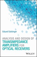
The p–i–n photodetector (or p–i–n photodiode) shown schematically in Fig. 3.1(a) and (b) is one of the simplest detectors. It consists of a p–n junction with a layer of intrinsic (undoped or lightly doped) semiconductor material sandwiched in between the p- and the n-doped material. The junction is reverse biased with ![]() to create a strong electric field in the intrinsic layer. The light enters through a hole in the top electrode (anode), passes through the p-doped material, and reaches the i-layer, which is also known as the absorption layer. The photons incident on the absorption layer knock electrons from the valence band to the conduction band creating electron–hole pairs. These pairs become separated by the strong electric drift field with the holes traveling to the negative terminal and the electrons traveling to the positive terminal, as indicated in Fig. 3.1(a). As a result, the photocurrent
to create a strong electric field in the intrinsic layer. The light enters through a hole in the top electrode (anode), passes through the p-doped material, and reaches the i-layer, which is also known as the absorption layer. The photons incident on the absorption layer knock electrons from the valence band to the conduction band creating electron–hole pairs. These pairs become separated by the strong electric drift field with the holes traveling to the negative terminal and the electrons traveling to the positive terminal, as indicated in Fig. 3.1(a). As a result, the photocurrent ![]() appears at the diode terminals. Figure 3.1(c) shows the circuit symbol for the photodiode.
appears at the diode terminals. Figure 3.1(c) shows the circuit symbol for the photodiode.
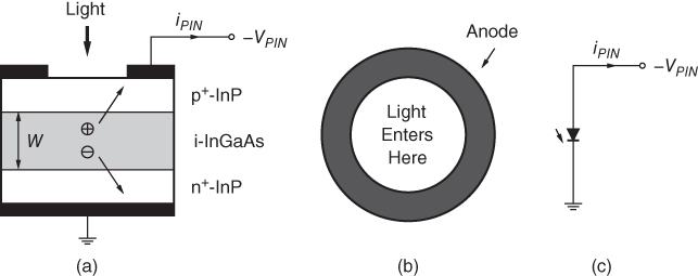
Figure 3.1 Vertically illuminated p–i–n photodetector: (a) cross-sectional view, (b) top view, and (c) circuit symbol.
Quantum Efficiency
The fraction of incident photons that results in electron–hole pairs contributing to the photocurrent is an important performance parameter known as the quantum efficiency ![]() . An ideal photodetector has a 100% quantum efficiency,
. An ideal photodetector has a 100% quantum efficiency, ![]() .
.
In a vertically illuminated photodetector, as the one in Fig. 3.1, the quantum efficiency depends on the width ![]() of the absorption layer. The wider
of the absorption layer. The wider ![]() is made, the better the chances that a photon is absorbed in this layer become. More specifically, the photon absorption efficiency is
is made, the better the chances that a photon is absorbed in this layer become. More specifically, the photon absorption efficiency is ![]() , where
, where ![]() is the absorption length (a.k.a. penetration depth). The InGaAs material, for example, has an absorption length of about
is the absorption length (a.k.a. penetration depth). The InGaAs material, for example, has an absorption length of about ![]() when illuminated at the 1.3 to 1.5-
when illuminated at the 1.3 to 1.5-![]() wavelength [1, 2]. If the absorption layer width is made equal to the absorption length (
wavelength [1, 2]. If the absorption layer width is made equal to the absorption length (![]() ), the photon absorption efficiency is around 63%; for widths much larger than the absorption length, the photon absorption efficiency asymptotically approaches 100%; for widths much smaller than the absorption length, the photon absorption efficiency is approximately proportional to
), the photon absorption efficiency is around 63%; for widths much larger than the absorption length, the photon absorption efficiency asymptotically approaches 100%; for widths much smaller than the absorption length, the photon absorption efficiency is approximately proportional to ![]() . A technique for improving the photon absorption efficiency is to make the bottom electrode reflective thus sending the not-yet-absorbed photons back up into the absorption layer giving them another chance to make a useful contribution to the photocurrent (double-pass scheme) [3].
. A technique for improving the photon absorption efficiency is to make the bottom electrode reflective thus sending the not-yet-absorbed photons back up into the absorption layer giving them another chance to make a useful contribution to the photocurrent (double-pass scheme) [3].
The quantum efficiency also depends on how much light is coupled from the fiber into the detector. To that end, the sensitive area of the photodetector should be made large enough to completely cover the light spot from the fiber and the detector's surface should be covered with an antireflection coating to maximize the light entering the detector. Another factor affecting the quantum efficiency is the fraction of electron–hole pairs that is collected by the electrodes and contributes to the photocurrent as opposed to the fraction that is lost to recombination.
Overall, the quantum efficiency can be understood as the product of three factors: fiber-to-detector coupling efficiency, photon absorption efficiency, and electron–hole pair collection efficiency. Sometimes the term external quantum efficiency is used for this overall quantum efficiency, whereas the term internal quantum efficiency refers to an internal aspects of the detection process, such as the photon absorption efficiency [3] or the electron–hole pair collection efficiency [4]. (Caution: Not all authors use these two terms in the same way.)
Spectral Response
Most semiconductor materials are transparent at the 1.3- and 1.55-![]() wavelengths commonly used in telecommunication applications, that is, they do not absorb photons at these wavelengths. For example, silicon absorbs photons for
wavelengths commonly used in telecommunication applications, that is, they do not absorb photons at these wavelengths. For example, silicon absorbs photons for ![]() only, gallium arsenide (GaAs) for
only, gallium arsenide (GaAs) for ![]() only, and indium phosphide (InP) for
only, and indium phosphide (InP) for ![]() only [2]. For a semiconductor to absorb photons, its bandgap energy
only [2]. For a semiconductor to absorb photons, its bandgap energy ![]() must be smaller than the photon energy:
must be smaller than the photon energy: ![]() , where
, where ![]() is the Planck constant. Only then do the photons have enough punch to knock electrons from the valence band into the conduction band. Therefore, the absorption layer in a photodetector must be made of a semiconductor compound with a sufficiently narrow bandgap. Nevertheless, the bandgap should not be made too narrow either to avoid an excessive thermally generated dark current.
is the Planck constant. Only then do the photons have enough punch to knock electrons from the valence band into the conduction band. Therefore, the absorption layer in a photodetector must be made of a semiconductor compound with a sufficiently narrow bandgap. Nevertheless, the bandgap should not be made too narrow either to avoid an excessive thermally generated dark current.
The quantum efficiency of a photodetector degrades toward the long-wavelength and the short-wavelength ends of the spectrum. The long-wavelength cutoff results from a lack of absorption when the photon energy drops below the bandgap energy, as discussed earlier. Interestingly, for high-energy photons (short wavelengths) the absorption length becomes so short that most photons are absorbed near the surface where many of the generated electron–hole pairs recombine before they reach the electrodes [5]. In other words, at long wavelengths the detector is limited by a low photon absorption efficiency and at short wavelengths the detector is limited by a low electron–hole pair collection efficiency.
For photodetectors that are sensitive at the 1.3- and 1.55-![]() wavelengths, a common choice for the absorption-layer material is indium gallium arsenide (InGaAs or more precisely
wavelengths, a common choice for the absorption-layer material is indium gallium arsenide (InGaAs or more precisely ![]() ), which has the important property of being lattice matched to the InP substrate (cf. Fig. 3.1(a)). InGaAs has a bandgap of
), which has the important property of being lattice matched to the InP substrate (cf. Fig. 3.1(a)). InGaAs has a bandgap of ![]() making the detector sensitive to wavelengths with
making the detector sensitive to wavelengths with ![]() [2]. Choosing InP for the p- and n-layers has the advantage that they are transparent at the wavelengths of interest, permitting a top or bottom illumination of the InGaAs absorption layer. Another absorption-layer material suitable for the 1.3- and 1.55-
[2]. Choosing InP for the p- and n-layers has the advantage that they are transparent at the wavelengths of interest, permitting a top or bottom illumination of the InGaAs absorption layer. Another absorption-layer material suitable for the 1.3- and 1.55-![]() wavelengths is germanium (Ge). It has a bandgap of
wavelengths is germanium (Ge). It has a bandgap of ![]() and can be grown on a silicon substrate by epitaxy (4% lattice mismatch), making it of particular interest for silicon photonics.
and can be grown on a silicon substrate by epitaxy (4% lattice mismatch), making it of particular interest for silicon photonics.
Detectors for the 0.85-![]() wavelength (commonly used in data-communication applications) are typically based on silicon or GaAs. Whereas silicon is lower in cost, GaAs offers a higher speed. Silicon has a longer absorption length than GaAs, because its indirect bandgap (at
wavelength (commonly used in data-communication applications) are typically based on silicon or GaAs. Whereas silicon is lower in cost, GaAs offers a higher speed. Silicon has a longer absorption length than GaAs, because its indirect bandgap (at ![]() ) requires the participation of a phonon to conserve momentum as well as energy. This low absorption rate must be compensated with a wider absorption layer, which makes the silicon detector slower [1, 2].
) requires the participation of a phonon to conserve momentum as well as energy. This low absorption rate must be compensated with a wider absorption layer, which makes the silicon detector slower [1, 2].
Bandwidth
The speed of a p–i–n photodetector depends mainly on the following factors: the width of the absorption layer ![]() , the reverse bias voltage
, the reverse bias voltage ![]() , the presence of slow diffusion currents, the photodiode capacitance, and packaging parasitics. We briefly discuss these factors in this order.
, the presence of slow diffusion currents, the photodiode capacitance, and packaging parasitics. We briefly discuss these factors in this order.
The width of the absorption layer ![]() determines the time it takes for the electrons and holes to traverse it. To obtain a fast response, this transit time must be kept short. For example, whereas
determines the time it takes for the electrons and holes to traverse it. To obtain a fast response, this transit time must be kept short. For example, whereas ![]() is fine for a 10-GHz InGaAs photodetector [6], the width must be reduced to
is fine for a 10-GHz InGaAs photodetector [6], the width must be reduced to ![]() for a 40-GHz detector [7] or even
for a 40-GHz detector [7] or even ![]() for a 100-GHz detector [3]. The problem with reducing
for a 100-GHz detector [3]. The problem with reducing ![]() is that it also reduces the quantum efficiency. Whereas a 10-GHz detector still has a good quantum efficiency (its absorption layer width is more than twice the absorption length), at
is that it also reduces the quantum efficiency. Whereas a 10-GHz detector still has a good quantum efficiency (its absorption layer width is more than twice the absorption length), at ![]() and above the quantum efficiency quickly becomes unacceptable, prompting an alternative photodetector design. The solution is to replace the vertically illuminated p–i–n detector from Fig. 3.1(a) with a so-called edge-coupled photodetector, which we discuss shortly.
and above the quantum efficiency quickly becomes unacceptable, prompting an alternative photodetector design. The solution is to replace the vertically illuminated p–i–n detector from Fig. 3.1(a) with a so-called edge-coupled photodetector, which we discuss shortly.
The transit time not only depends on the width ![]() but also on the strength of the electric drift field in the absorption layer. With increasing field strength
but also on the strength of the electric drift field in the absorption layer. With increasing field strength ![]() the carrier velocity increases and (after a possible velocity overshoot) saturates at
the carrier velocity increases and (after a possible velocity overshoot) saturates at ![]() . For holes in InGaAs
. For holes in InGaAs ![]() (for electrons
(for electrons ![]() ) and is reached for
) and is reached for ![]() [6]. Thus, to obtain the minimum transit time
[6]. Thus, to obtain the minimum transit time ![]() , the bias voltage,
, the bias voltage, ![]() , must be high enough such that velocity saturation is reached. For a 10-GHz photodetector the bandwidth saturates at around 4 to
, must be high enough such that velocity saturation is reached. For a 10-GHz photodetector the bandwidth saturates at around 4 to ![]() [6], for a 40-GHz detector at around 2 to
[6], for a 40-GHz detector at around 2 to ![]() [7], and for a 100-GHz detector at around 1.5 to
[7], and for a 100-GHz detector at around 1.5 to ![]() [3]. As the width of the absorption layer is reduced for higher speed devices, less voltage is needed to reach the field at which the velocity saturates. On the high end, the bias voltage is limited by the onset of avalanche breakdown. At this point, the reverse current increases rapidly, as illustrated in Fig. 3.2. (The
[3]. As the width of the absorption layer is reduced for higher speed devices, less voltage is needed to reach the field at which the velocity saturates. On the high end, the bias voltage is limited by the onset of avalanche breakdown. At this point, the reverse current increases rapidly, as illustrated in Fig. 3.2. (The ![]() characteristic of a dark p–i–n photodetector is identical to that of a regular p–n junction; when illuminated, it shifts down along the current axis by the amount of the photocurrent
characteristic of a dark p–i–n photodetector is identical to that of a regular p–n junction; when illuminated, it shifts down along the current axis by the amount of the photocurrent ![]() .) Power dissipation (
.) Power dissipation (![]() ) is another consideration limiting the bias voltage, especially when the photocurrent is large as, for example, in a coherent receiver.
) is another consideration limiting the bias voltage, especially when the photocurrent is large as, for example, in a coherent receiver.

Figure 3.2  characteristics of a dark and an illuminated p–i–n photodetector.
Photons absorbed outside of the drift field create slowly diffusing carriers, which when eventually stumbling into the drift field make a delayed contribution to the photocurrent. For example, photons absorbed in the (neutral) n-layer of a silicon p–i–n photodetector create electron–hole pairs. The holes, which are the minority carriers, take about ![]() to diffuse through
to diffuse through ![]() of silicon [2] (and four times as long for twice this distance). As a result, the desired current pulse corresponding to the optical signal is followed by a spurious current tail, as shown in Fig. 3.3(a) [1, 8]. In the frequency response, the diffusion currents manifest themselves as a hump at low frequencies, as shown in Fig. 3.3(b) [8]. Diffusion currents can be minimized by using either transparent materials for the p- and n-layers or by making the layers very thin and aligning the fiber precisely to the active part of the absorption layer. Diffusion currents are particularly bothersome in burst-mode receivers, where the tail of a very strong burst may mask the subsequent (weak) burst [9].
of silicon [2] (and four times as long for twice this distance). As a result, the desired current pulse corresponding to the optical signal is followed by a spurious current tail, as shown in Fig. 3.3(a) [1, 8]. In the frequency response, the diffusion currents manifest themselves as a hump at low frequencies, as shown in Fig. 3.3(b) [8]. Diffusion currents can be minimized by using either transparent materials for the p- and n-layers or by making the layers very thin and aligning the fiber precisely to the active part of the absorption layer. Diffusion currents are particularly bothersome in burst-mode receivers, where the tail of a very strong burst may mask the subsequent (weak) burst [9].

Figure 3.3 Impact of diffusion currents in (a) the time domain and (b) the frequency domain.
The capacitance of the p–i–n photodetector ![]() together with the contact and load resistance present another speed limitation. Figure 3.4(a) shows an equivalent AC circuit for a bare p–i–n photodetector (without packaging parasitics). The current source
together with the contact and load resistance present another speed limitation. Figure 3.4(a) shows an equivalent AC circuit for a bare p–i–n photodetector (without packaging parasitics). The current source ![]() represents the photocurrent generated in the p–i–n structure. Besides the photodiode junction capacitance
represents the photocurrent generated in the p–i–n structure. Besides the photodiode junction capacitance ![]() , the combination of contact and spreading resistance is modeled by
, the combination of contact and spreading resistance is modeled by ![]() . Given the load resistance
. Given the load resistance ![]() , often assumed to be
, often assumed to be ![]() , the time constant of this
, the time constant of this ![]() network is
network is ![]() .
.

Figure 3.4 Equivalent AC circuits for 10- p–i–n photodetectors: (a) bare photodiode [10] and (b) photodiode with packaging parasitics [11].
The bandwidth due to this ![]() network alone, that is, the
network alone, that is, the ![]() -limited bandwidth, follows easily as
-limited bandwidth, follows easily as ![]() . The bandwidth due to the transit time alone, that is, the transit-time-limited bandwidth, can be approximated as
. The bandwidth due to the transit time alone, that is, the transit-time-limited bandwidth, can be approximated as ![]() . (The numerical factor is given variously as 2.4 [5], 2.8 [12], 2.4 to 3.4 [4], and 3.5 [3].) Combining these two bandwidths results in the following bandwidth estimate for the bare p–i–n photodiode [3]:
. (The numerical factor is given variously as 2.4 [5], 2.8 [12], 2.4 to 3.4 [4], and 3.5 [3].) Combining these two bandwidths results in the following bandwidth estimate for the bare p–i–n photodiode [3]:

As we make the absorption layer thinner and thinner to reduce the transit time, unfortunately, the diode capacitance gets larger and larger, possibly making the ![]() time constant in Eq. (3.1) the dominant contribution. One solution is to reduce the area of the photodetector (which, however, may also reduce the coupling efficiency), another solution is to replace the lumped photodiode capacitance with a distributed one, leading to the traveling-wave photodetector, which we discuss shortly.
time constant in Eq. (3.1) the dominant contribution. One solution is to reduce the area of the photodetector (which, however, may also reduce the coupling efficiency), another solution is to replace the lumped photodiode capacitance with a distributed one, leading to the traveling-wave photodetector, which we discuss shortly.
In addition to ![]() and
and ![]() , the packaged photodetector has
, the packaged photodetector has ![]() parasitics caused by wire bonds, lead frames, and so forth, as shown in Fig. 3.4(b). In high-speed photodetectors, these parasitics can significantly impact the overall bandwidth and close attention must be payed to them [3, 6].
parasitics caused by wire bonds, lead frames, and so forth, as shown in Fig. 3.4(b). In high-speed photodetectors, these parasitics can significantly impact the overall bandwidth and close attention must be payed to them [3, 6].
The equivalent AC circuits in Fig. 3.4 can be extended to model the transit-time effect by replacing the current source ![]() with a voltage-controlled current source, connected to the output of a noiseless
with a voltage-controlled current source, connected to the output of a noiseless ![]() low-pass filter with time constant
low-pass filter with time constant ![]() [13].
[13].
p–i–n Photodetectors for 40 Gb/s and Faster
As we have seen, the vertically illuminated photodetector suffers from a rapidly diminishing quantum efficiency at speeds of ![]() and above. The bandwidth-efficiency product (
and above. The bandwidth-efficiency product (![]() ) of vertically illuminated p–i–n detectors tops out at about 20 to
) of vertically illuminated p–i–n detectors tops out at about 20 to ![]() [14]. This issue can be resolved by illuminating the photodetector from the side rather than from the top, as shown in Fig. 3.5. This configuration is known as an edge-coupled photodetector or a waveguide photodetector. Now, the quantum efficiency is controlled by the horizontal dimension, which can be made large, whereas the transit time is controlled by the vertical dimension
[14]. This issue can be resolved by illuminating the photodetector from the side rather than from the top, as shown in Fig. 3.5. This configuration is known as an edge-coupled photodetector or a waveguide photodetector. Now, the quantum efficiency is controlled by the horizontal dimension, which can be made large, whereas the transit time is controlled by the vertical dimension ![]() , which can be made small.
, which can be made small.
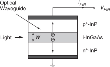
Figure 3.5 Waveguide p–i–n photodetector.
However, this is easier said than done. The main difficulty is to efficiently couple the light from the fiber with a core of 8 to ![]() into the absorption layer with a submicrometer width. For comparison, vertically illuminated photodetectors have a diameter of
into the absorption layer with a submicrometer width. For comparison, vertically illuminated photodetectors have a diameter of ![]() or more. Even when focused by a lens, the light spot is still too large for the thin absorption layer. One solution, the so-called double-core waveguide photodetector, is to embed the thin absorption layer into a larger optical multimode waveguide that couples more efficiently to the external fiber [3]. Another solution, the so-called evanescently coupled waveguide photodetector, is to place an optical waveguide designed for good coupling with the external fiber in parallel to (but outside of) the absorption layer and take advantage of the evanescent field (near field), which extends outside of the optical waveguide, to do the coupling [3].
or more. Even when focused by a lens, the light spot is still too large for the thin absorption layer. One solution, the so-called double-core waveguide photodetector, is to embed the thin absorption layer into a larger optical multimode waveguide that couples more efficiently to the external fiber [3]. Another solution, the so-called evanescently coupled waveguide photodetector, is to place an optical waveguide designed for good coupling with the external fiber in parallel to (but outside of) the absorption layer and take advantage of the evanescent field (near field), which extends outside of the optical waveguide, to do the coupling [3].
For example, the 40-![]() InGaAs evanescently coupled waveguide photodetector reported in [7] achieves a 47-GHz bandwidth and a 65% quantum efficiency, the InGaAs double-core waveguide photodetector in [3] achieves a 110-GHz bandwidth and a 50% quantum efficiency, and the GaAs (short wavelength) waveguide photodetector in [15] achieves a 118-GHz bandwidth and a 49% quantum efficiency. For a packaged waveguide p–i–n photodetector, see Fig. 3.7.
InGaAs evanescently coupled waveguide photodetector reported in [7] achieves a 47-GHz bandwidth and a 65% quantum efficiency, the InGaAs double-core waveguide photodetector in [3] achieves a 110-GHz bandwidth and a 50% quantum efficiency, and the GaAs (short wavelength) waveguide photodetector in [15] achieves a 118-GHz bandwidth and a 49% quantum efficiency. For a packaged waveguide p–i–n photodetector, see Fig. 3.7.
Even after edge coupling, the photodiode junction capacitance and its associated ![]() time constant is still a limiting factor, especially for high-speed detectors. The solution to this problem is to replace the photodiode contact pad by a terminated transmission line. The transmission line still has a large capacitance, but now it is distributed in between inductive elements that make the overall transmission line impedance real valued. Figure 3.6 shows a so-called traveling-wave photodetector terminated by the resistor
time constant is still a limiting factor, especially for high-speed detectors. The solution to this problem is to replace the photodiode contact pad by a terminated transmission line. The transmission line still has a large capacitance, but now it is distributed in between inductive elements that make the overall transmission line impedance real valued. Figure 3.6 shows a so-called traveling-wave photodetector terminated by the resistor ![]() , which matches the characteristic impedance of the transmission line. The light pulse enters from the left and gets weaker and weaker as it travels through the absorption layer. The photogenerated carriers get collected by the waveguide at the top producing a stronger and stronger electrical pulse as it travels to the right. The top view in Fig. 3.6(b) shows how the photodiode electrode is made part of a coplanar waveguide. The idea behind the traveling-wave photodetector is the same as that behind the distributed amplifier (cf. Section 7.8), except that the electrical input is replaced by an optical input.
, which matches the characteristic impedance of the transmission line. The light pulse enters from the left and gets weaker and weaker as it travels through the absorption layer. The photogenerated carriers get collected by the waveguide at the top producing a stronger and stronger electrical pulse as it travels to the right. The top view in Fig. 3.6(b) shows how the photodiode electrode is made part of a coplanar waveguide. The idea behind the traveling-wave photodetector is the same as that behind the distributed amplifier (cf. Section 7.8), except that the electrical input is replaced by an optical input.
Figure 3.6 Traveling-wave p–i–n photodetector: (a) cross-sectional view and (b) top view (different scale).
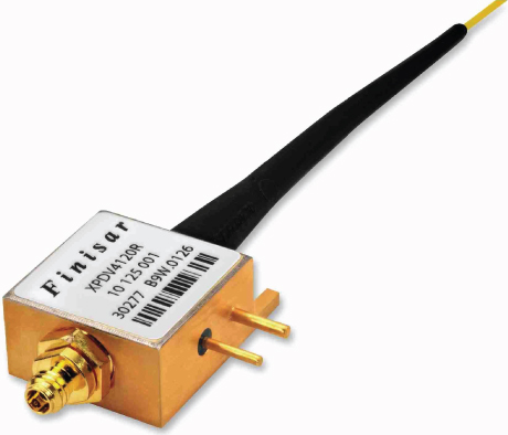
Figure 3.7 A packaged 100- waveguide p–i–n photodetector with biasing network and single-mode fiber pigtail (
 ).
).
Source: Reprinted by permission from Finisar Corporation.
In principle, the bandwidth of the traveling-wave photodetector is independent of the detector's length. However, in practice the bandwidth is limited by the velocity mismatch between the optical traveling wave and the electrical traveling wave, which is not easy to keep small [3]. Another issue is the backward-traveling electrical wave, which can be terminated into another resistor (![]() with dashed lines in Fig. 3.6(a)) or can be left open. In the first case, the efficiency is cut in half as a result of the current lost in the back termination; in the second case, the reflected backward-traveling wave reduces the bandwidth of the photodetector, especially when the photodetector is long [3].
with dashed lines in Fig. 3.6(a)) or can be left open. In the first case, the efficiency is cut in half as a result of the current lost in the back termination; in the second case, the reflected backward-traveling wave reduces the bandwidth of the photodetector, especially when the photodetector is long [3].
For example, the GaAs traveling-wave photodetector reported in [15] achieves a 172-GHz bandwidth and a 42% quantum efficiency, demonstrating the very high bandwidth-efficiency product of ![]() .
.
Responsivity
Let us calculate the current ![]() produced by a p–i–n photodetector that is illuminated with the optical power
produced by a p–i–n photodetector that is illuminated with the optical power ![]() . Each photon has the energy
. Each photon has the energy ![]() . Given the incident optical power
. Given the incident optical power ![]() , the photons must arrive at the average rate
, the photons must arrive at the average rate ![]() . Of all those photons, the fraction
. Of all those photons, the fraction ![]() creates electron–hole pairs that contribute to the photocurrent. Thus the average electron rate becomes
creates electron–hole pairs that contribute to the photocurrent. Thus the average electron rate becomes ![]() . Multiplying this rate by the electron charge
. Multiplying this rate by the electron charge ![]() gives us the “charge rate,” which is nothing else but the photocurrent:
gives us the “charge rate,” which is nothing else but the photocurrent:
The factor relating ![]() to
to ![]() is known as the responsivity of the photodetector and is designated by the symbol
is known as the responsivity of the photodetector and is designated by the symbol ![]() :
:
For example, for the commonly used wavelength ![]() and the quantum efficiency
and the quantum efficiency ![]() , we obtain the responsivity
, we obtain the responsivity ![]() . This means that for every milliwatt of optical power incident onto the photodetector, we obtain
. This means that for every milliwatt of optical power incident onto the photodetector, we obtain ![]() of current. The responsivity of a typical InGaAs p–i–n photodetector is in the range 0.6 to
of current. The responsivity of a typical InGaAs p–i–n photodetector is in the range 0.6 to ![]() [1].
[1].
A Two-for-One Special
The relationship in Eq. (3.3) has an interesting property: If we double the light power, the photodiode current doubles as well. Now this is very odd! Usually, power is related to the square of the current rather than the current directly. For example, if we double the RF power radiated at a wireless receiver, the antenna current increases by a factor ![]() . Or, if we double the current flowing through a resistor, the power dissipated into heat increases by
. Or, if we double the current flowing through a resistor, the power dissipated into heat increases by ![]() . This square-law relationship between power and current is the reason why we use “
. This square-law relationship between power and current is the reason why we use “![]() ” to calculate power dBs and “
” to calculate power dBs and “![]() ” to calculate current or voltage dBs. When using this convention, a 3-dB increase in RF power translates into a 3-dB increase in antenna current, or a 6-dB increase in current results in a 6-dB increase in power dissipation in the resistor. For a photodetector, however, a 3-dB increase in optical power translates into a 6-dB increase in current. What a bargain! [
” to calculate current or voltage dBs. When using this convention, a 3-dB increase in RF power translates into a 3-dB increase in antenna current, or a 6-dB increase in current results in a 6-dB increase in power dissipation in the resistor. For a photodetector, however, a 3-dB increase in optical power translates into a 6-dB increase in current. What a bargain! [![]() Problems 3.1 and 3.2.]
Problems 3.1 and 3.2.]
Wireless Receiver with a Photodetector?
Unlike optical receivers, wireless receivers use antennas to detect electromagnetic waves. The rms current that is produced by an antenna under matched conditions is [16]

where ![]() is the received power (more precisely, the power incident on the effective aperture of the antenna) and
is the received power (more precisely, the power incident on the effective aperture of the antenna) and ![]() is the antenna resistance. For example, for a
is the antenna resistance. For example, for a ![]() signal (
signal (![]() ), we obtain approximately
), we obtain approximately ![]() rms from an antenna with
rms from an antenna with ![]() .
.
What if we replace our antenna with a hypothetical hyperinfrared photodetector that can detect a 1-GHz RF signal? Let us assume we succeeded in making a photodetector with a very small bandgap that is sensitive to low-energy RF photons (![]() ) and suppressing thermally generated dark currents by cooling the detector to a millikelvin or so. We can then calculate the responsivity of this detector with Eq. (3.3) to be an impressive
) and suppressing thermally generated dark currents by cooling the detector to a millikelvin or so. We can then calculate the responsivity of this detector with Eq. (3.3) to be an impressive ![]() assuming that
assuming that ![]() and
and ![]() . So, for the same received power level of
. So, for the same received power level of ![]() , we obtain a current of
, we obtain a current of ![]() , that is, almost
, that is, almost ![]() more than with the old-fashioned antenna! The reason for this, of course, is that the photodetector produces a current proportional to the square of the electromagnetic field, whereas the antenna produces a current directly proportional to the field.
more than with the old-fashioned antenna! The reason for this, of course, is that the photodetector produces a current proportional to the square of the electromagnetic field, whereas the antenna produces a current directly proportional to the field.
But do not launch your start-up company to market this idea just yet! What happens if we reduce the received power? After all, it is for weak signals where the detector's responsivity matters the most. The signal from the photodetector decreases linearly, whereas the signal from the antenna decreases more slowly following a square-root law. Once we are down to ![]() (
(![]() ), we obtain approximately
), we obtain approximately ![]() from the antenna and
from the antenna and ![]() from the photodetector (see Fig. 3.8), which is about the same!
from the photodetector (see Fig. 3.8), which is about the same!

Figure 3.8 Responsivity of an antenna and a photodetector at  .
.
The aforementioned comparison is meant to illustrate signal detection laws and for simplicity disregards detector noise. To be fair, we should compare the detector sensitivities defined as the (optical or RF) input power required to make the (electrical) output signal power equal to the (electrical) output noise power. Even then, it turns out that the regular antenna already reaches the fundamental sensitivity limit [17], leaving no hope for the photodetector to beat it. [![]() Problem 3.3.]
Problem 3.3.]
Optical Receiver with an Antenna?
What is the fundamental reason why photodetectors respond to the intensity rather than to the optical field? The processes within the photodetector (carrier transport and relaxation processes) are too slow to track the rapid field variations that occur at around ![]() [18].
[18].
Could we help the detector by converting the optical frequencies down to RF frequencies using a mixer and a local oscillator just like in a superheterodyne radio receiver? Yes, this is possible with the heterodyne receiver1 setup shown in Fig. 3.9. The incoming optical signal is combined with (added to) the beam of a continuous-wave laser operating at a frequency that is offset by, say, ![]() from the signal frequency. The latter laser source is known as the local oscillator (LO). The square-law photodetector acts as the mixer nonlinearity producing a spectral component at the 1-GHz intermediate frequency (IF).
from the signal frequency. The latter laser source is known as the local oscillator (LO). The square-law photodetector acts as the mixer nonlinearity producing a spectral component at the 1-GHz intermediate frequency (IF).
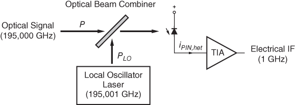
Figure 3.9 Optical heterodyne receiver.
The rms current that is produced by the optical heterodyne receiver is [1, 2]
where ![]() is the received power,
is the received power, ![]() is the power of the LO, and
is the power of the LO, and ![]() is assumed. Lo and behold, the current is now proportional to the square root of the power, just like for an antenna! We have converted a square-law detector into a linear one. Besides the detection law, the optical heterodyne receiver shares several other properties with the antenna of an RF receiver [19].
is assumed. Lo and behold, the current is now proportional to the square root of the power, just like for an antenna! We have converted a square-law detector into a linear one. Besides the detection law, the optical heterodyne receiver shares several other properties with the antenna of an RF receiver [19].
Unlike our hypothetical hyperinfrared photodiode, the optical heterodyne receiver is a practical invention used in many commercial products. It and other coherent receivers have been studied thoroughly [1, 2]. The heterodyne receiver is sensitive to the phase of the incoming signal, permitting the reception of phase-modulated optical signals. We continue the discussion of coherent receivers in Section 3.5.
Shot Noise
A p–i–n photodetector illuminated by a noise-free (coherent) continuous-wave source not only produces the DC current ![]() but also a noise current known as shot noise. This fundamental noise appears because the photocurrent is composed of a large number of short pulses that are distributed randomly in time. Each pulse is caused by an electron–hole pair, which in turn was created by an absorbed photon. The area under each pulse (its integral over time) equals the electron charge
but also a noise current known as shot noise. This fundamental noise appears because the photocurrent is composed of a large number of short pulses that are distributed randomly in time. Each pulse is caused by an electron–hole pair, which in turn was created by an absorbed photon. The area under each pulse (its integral over time) equals the electron charge ![]() . If we approximate these pulses with Dirac delta functions, we obtain the instantaneous current shown in Fig. 3.10(a). In practice, the bandwidth of the photodetector is finite causing the individual pulses to smear out and overlap. To analyze the band-limited shot noise, we make use of the conceptually simple rectangular filter, which outputs the moving average over the time window
. If we approximate these pulses with Dirac delta functions, we obtain the instantaneous current shown in Fig. 3.10(a). In practice, the bandwidth of the photodetector is finite causing the individual pulses to smear out and overlap. To analyze the band-limited shot noise, we make use of the conceptually simple rectangular filter, which outputs the moving average over the time window ![]() (cf. Section 4.8). Filtered in this way, the band-limited current can be written as
(cf. Section 4.8). Filtered in this way, the band-limited current can be written as ![]() , where
, where ![]() is the number of pulses falling into the window starting at time
is the number of pulses falling into the window starting at time ![]() and ending at time
and ending at time ![]() . The band-limited current, illustrated in Fig. 3.10(b), can be thought of as a superposition of the average photocurrent
. The band-limited current, illustrated in Fig. 3.10(b), can be thought of as a superposition of the average photocurrent ![]() and the shot-noise fluctuations. The average current is
and the shot-noise fluctuations. The average current is ![]() , where
, where ![]() is the average number of pulses falling into the window
is the average number of pulses falling into the window ![]() .
.
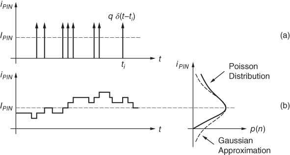
Figure 3.10 Fluctuations in the (a) wide-band and (b) band-limited photocurrent (ps scale).
For example, a received optical power of ![]() generates an average current of
generates an average current of ![]() , assuming
, assuming ![]() . From
. From ![]() , we can calculate that the electrons in this current move at an average rate of five electrons per picosecond (
, we can calculate that the electrons in this current move at an average rate of five electrons per picosecond (![]() and
and ![]() ). If the electrons were marching through the detector like little soldiers, with exactly five passing every picosecond, then the band-limited photocurrent would be noise free. However, in reality the electrons are moving randomly and shot noise is produced. For a coherent optical source, the number of electrons passing through the detector during the time interval
). If the electrons were marching through the detector like little soldiers, with exactly five passing every picosecond, then the band-limited photocurrent would be noise free. However, in reality the electrons are moving randomly and shot noise is produced. For a coherent optical source, the number of electrons passing through the detector during the time interval ![]() follows a Poisson distribution:
follows a Poisson distribution:
where ![]() and
and ![]() . This distribution is shown on the far right of Fig. 3.10(b). Note its asymmetric shape: whereas the current never becomes negative, there is a chance that the current exceeds
. This distribution is shown on the far right of Fig. 3.10(b). Note its asymmetric shape: whereas the current never becomes negative, there is a chance that the current exceeds ![]() . For this reason, the Gaussian distribution (shown with a dashed line in Fig. 3.10(b)) cannot accurately describe the distribution. However, the larger the average
. For this reason, the Gaussian distribution (shown with a dashed line in Fig. 3.10(b)) cannot accurately describe the distribution. However, the larger the average ![]() becomes, the better the Gaussian approximation fits. For small photocurrents,
becomes, the better the Gaussian approximation fits. For small photocurrents, ![]() , the Poisson distribution must be used, but for large currents, the Gaussian distribution may be a more convenient choice.
, the Poisson distribution must be used, but for large currents, the Gaussian distribution may be a more convenient choice.
We are now ready to derive the mean-square value of the shot noise [17, 20]. The standard deviation of a Poisson distribution with average ![]() is
is ![]() . Thus the rms noise current is
. Thus the rms noise current is ![]() and the mean-square noise current is
and the mean-square noise current is ![]() . Inserting
. Inserting ![]() for the average number of electrons, we find
for the average number of electrons, we find ![]() . Finally, using the fact that the noise bandwidth of the rectangular filter is
. Finally, using the fact that the noise bandwidth of the rectangular filter is ![]() (cf. Section 4.8), the mean-square value of the shot noise measured in the bandwidth
(cf. Section 4.8), the mean-square value of the shot noise measured in the bandwidth ![]() becomes
becomes
Thus, the 0.8-![]() current from our earlier example produces a shot-noise current of about
current from our earlier example produces a shot-noise current of about ![]() rms in a 10-GHz bandwidth. The signal-to-noise ratio of this DC current can be calculated as
rms in a 10-GHz bandwidth. The signal-to-noise ratio of this DC current can be calculated as ![]() . [
. [![]() Problem 3.4.]
Problem 3.4.]
The power spectral density (PSD) of the wide-band photocurrent in Fig. 3.10(a) is shown in Fig. 3.11(a). It has a Dirac delta function at DC, which corresponds to the average signal current ![]() and a white noise component with the (one-sided) PSD
and a white noise component with the (one-sided) PSD ![]() , which corresponds to the shot noise.2 The PSD of the band-limited photocurrent, shown in Fig. 3.11(b), is shaped by the low-pass response of the rectangular filter. The shot-noise PSD becomes
, which corresponds to the shot noise.2 The PSD of the band-limited photocurrent, shown in Fig. 3.11(b), is shaped by the low-pass response of the rectangular filter. The shot-noise PSD becomes ![]() , where
, where ![]() is the frequency response of the rectangular filter.
is the frequency response of the rectangular filter.

Figure 3.11 Power spectral density of the (a) wide-band and (b) band-limited photocurrent.
It is clear from the aforementioned considerations and Eq. (3.7) that the shot-noise current is signal dependent, that is, it is a function of ![]() . If the received optical power increases, the noise increases, too. But fortunately, the rms noise grows only with the square root of the signal amplitude, so we still gain in terms of signal-to-noise ratio. If we double the optical power in our previous example from 1 to
. If the received optical power increases, the noise increases, too. But fortunately, the rms noise grows only with the square root of the signal amplitude, so we still gain in terms of signal-to-noise ratio. If we double the optical power in our previous example from 1 to ![]() , we obtain an average current of
, we obtain an average current of ![]() and a shot-noise current of
and a shot-noise current of ![]() ; thus, the signal-to-noise ratio improved by
; thus, the signal-to-noise ratio improved by ![]() from 24 to
from 24 to ![]() . Conversely, if the received optical power is reduced, the noise reduces, too. For example, if we reduce the optical power by
. Conversely, if the received optical power is reduced, the noise reduces, too. For example, if we reduce the optical power by ![]() , the signal current reduces by
, the signal current reduces by ![]() , but the signal-to-noise ratio degrades by only
, but the signal-to-noise ratio degrades by only ![]() .
.
If we receive a (noise free) non-return-to-zero (NRZ) signal with a p–i–n photodetector, the electrical noise on the one bits is much larger than that on the zero bits. In fact, if the transmitter light source turns off completely during the transmission of zeros (infinite extinction ratio) and the photodetector is free of dark current (to be discussed shortly), then there is no current and therefore no shot noise. Let us suppose that the received optical signal is DC balanced (same numbers of zeros and ones), has a high extinction ratio, and has the average power ![]() . Then, the optical power for the ones is
. Then, the optical power for the ones is ![]() and that for the zeros is
and that for the zeros is ![]() . Thus with Eq. (3.7), we find the noise currents for zeros and ones to be
. Thus with Eq. (3.7), we find the noise currents for zeros and ones to be
If incomplete extinction and the dark current are taken into account, ![]() . Figure 3.12 illustrates the signal and noise currents produced by a p–i–n photodetector in response to an optical NRZ signal with DC balance and high extinction. Signal and noise magnitudes are expressed in terms of the average received power
. Figure 3.12 illustrates the signal and noise currents produced by a p–i–n photodetector in response to an optical NRZ signal with DC balance and high extinction. Signal and noise magnitudes are expressed in terms of the average received power ![]() .
.
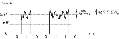
Figure 3.12 Signal and noise currents from a p–i–n photodetector.
Dark Current
The p–i–n photodetector produces a small amount of current even when it is in total darkness. This so-called dark current, ![]() , depends on the diode material, temperature, reverse bias, junction area, and processing. For a high-speed InGaAs photodetector at room temperature and a reverse bias of
, depends on the diode material, temperature, reverse bias, junction area, and processing. For a high-speed InGaAs photodetector at room temperature and a reverse bias of ![]() , it is usually less than
, it is usually less than ![]() . Photodiodes made from materials with a smaller bandgap (such as germanium) suffer from a larger dark current because thermally generated electron–hole pairs become more numerous at a given temperature. Similarly, the dark current increases with temperature because the electrons become more energetic and thus are more likely to jump across a given bandgap.
. Photodiodes made from materials with a smaller bandgap (such as germanium) suffer from a larger dark current because thermally generated electron–hole pairs become more numerous at a given temperature. Similarly, the dark current increases with temperature because the electrons become more energetic and thus are more likely to jump across a given bandgap.
The dark current and its associated shot-noise current interfere with the received signal. Fortunately, in high-speed p–i–n receivers (![]() ), this effect usually is negligible. Let us calculate the optical power for which the worst-case dark current amounts to 10% of the signal current. As long as our received optical power is much larger than this, we are fine:
), this effect usually is negligible. Let us calculate the optical power for which the worst-case dark current amounts to 10% of the signal current. As long as our received optical power is much larger than this, we are fine:
With the values ![]() and
and ![]() , we find
, we find ![]() . In Section 4.4, we see that high-speed p–i–n receivers require much more signal power than this to work at an acceptable bit-error rate (to overcome the TIA noise), and therefore we do not need to worry about dark current in such receivers. However, in low-speed p–i–n receivers or APD receivers, the dark current can be an important limitation. In Section 4.7, we formulate the impact of dark current on the receiver sensitivity in a more precise way.
. In Section 4.4, we see that high-speed p–i–n receivers require much more signal power than this to work at an acceptable bit-error rate (to overcome the TIA noise), and therefore we do not need to worry about dark current in such receivers. However, in low-speed p–i–n receivers or APD receivers, the dark current can be an important limitation. In Section 4.7, we formulate the impact of dark current on the receiver sensitivity in a more precise way.
Saturation Current
Whereas the shot noise and the dark current determine the lower end of the p–i–n detector's dynamic range, the saturation current defines the upper end of this range. At very high optical power levels, a correspondingly high density of electron–hole pairs is produced, which results in a space charge that counteracts the bias-voltage induced drift field. The consequences are a decreased responsivity (gain compression) and a reduced bandwidth. Moreover, the power dissipated in the photodiode (![]() ) causes heating, which results in high dark currents or even the destruction of the device.
) causes heating, which results in high dark currents or even the destruction of the device.
For a photodiode preceded by an optical amplifier, such as an erbium-doped fiber amplifier (EDFA), its quantum efficiency and responsivity are of secondary importance (we discuss photodetectors with optical preamplifiers in Section 3.3). Low values of these parameters can be compensated for with a higher optical gain. In contrast, the bandwidth and the saturation current are of primary importance. The saturation current, in particular, limits the voltage swing that can be obtained by driving the photocurrent directly into a ![]() resistor. For example, the 80-
resistor. For example, the 80-![]() detector reviewed in [22] is capable of producing a 0.8-V swing, which is sufficient to directly drive a decision circuit.
detector reviewed in [22] is capable of producing a 0.8-V swing, which is sufficient to directly drive a decision circuit.
Photodiodes for analog applications, such as CATV/HFC, must be highly linear to minimize distortions in the sensitive analog signal (cf. Appendix D) and therefore must be operated well below their saturation current. A beam splitter, multiple photodetectors, and a power combiner can be used to increase the effective saturation current of the photodetector [23].
There are two approaches for increasing the saturation current of a photodiode. One way is to distribute the photogenerated carriers over a larger volume. In a vertically illuminated photodetector this can be done by overfilling the absorbing area such that 5 to 10% of the Gaussian beam is beyond the active region [14]. In an edge-coupled photodetector the carrier density can be reduced by making it longer, however, this measure may lower the bandwidth. The second way is to increase the carrier velocity by exploiting the fact that under certain conditions electrons (but not holes) can drift much faster (e.g., five times faster) than at their saturated velocity [3]. This fast drift velocity is known as the overshoot velocity. The latter approach led to the development of the uni-traveling-carrier (UTC) photodiode, which employs a modification of the p–i–n structure that eliminates the (slow) holes from participating in the photodetection process [22]. UTC photodiodes come in all the flavors known from p–i–n photodiodes: vertically illuminated, waveguide, and traveling wave. Some of the highest reported saturation currents for UTC photodiodes are in the 26 to ![]() range, whereas those for p–i–n photodiodes are in the 10 to
range, whereas those for p–i–n photodiodes are in the 10 to ![]() range [14].
range [14].
3.2 Avalanche Photodetector
The basic structure of the avalanche photodetector (APD) is shown in Fig. 3.13. Like the p–i–n detector, the avalanche photodetector is a reverse biased diode. However, in contrast to the p–i–n photodetector, it features an additional layer, the multiplication region. This layer provides internal gain through avalanche multiplication of the photogenerated carriers.

Figure 3.13 Avalanche photodetector (vertically illuminated structure).
The vertically illuminated InGaAs/InP APD, shown in Fig. 3.13, is sensitive to the 1.3 and 1.55-![]() wavelengths common in telecommunication systems. It operates as follows. The light enters through a hole in the top electrode and passes through the transparent InP layer to the InGaAs absorption layer. Just like in the p–i–n structure, electron–hole pairs are generated and separated by the electric field in the absorption layer. The holes move upward and enter the multiplication region. Accelerated by the strong electric field in this region the holes acquire sufficient energy to create secondary electron–hole pairs. This process is known as impact ionization. The figure shows one primary hole creating two secondary holes corresponding to an avalanche gain of three (
wavelengths common in telecommunication systems. It operates as follows. The light enters through a hole in the top electrode and passes through the transparent InP layer to the InGaAs absorption layer. Just like in the p–i–n structure, electron–hole pairs are generated and separated by the electric field in the absorption layer. The holes move upward and enter the multiplication region. Accelerated by the strong electric field in this region the holes acquire sufficient energy to create secondary electron–hole pairs. This process is known as impact ionization. The figure shows one primary hole creating two secondary holes corresponding to an avalanche gain of three (![]() ). In InP, holes are more ionizing than electrons hence the multiplication region is placed on the side of the absorption region where the primary holes exit. (In silicon, the opposite is true and the multiplication layer is placed on the other side.) Like for the p–i–n photodiode, the width of the absorption layer
). In InP, holes are more ionizing than electrons hence the multiplication region is placed on the side of the absorption region where the primary holes exit. (In silicon, the opposite is true and the multiplication layer is placed on the other side.) Like for the p–i–n photodiode, the width of the absorption layer ![]() impacts the quantum efficiency. The width of the multiplication layer
impacts the quantum efficiency. The width of the multiplication layer ![]() together with the bias voltage
together with the bias voltage ![]() determines the electric field in this layer. A smaller width leads to a stronger field. The wider bandgap InP material is chosen for the multiplication region because it can sustain a higher field than InGaAs and is transparent at the wavelengths of interest.
determines the electric field in this layer. A smaller width leads to a stronger field. The wider bandgap InP material is chosen for the multiplication region because it can sustain a higher field than InGaAs and is transparent at the wavelengths of interest.
In practice, APD structures are more complex than the one sketched in Fig. 3.13. A practical APD may include a guard ring to suppress leakage currents and edge breakdown, a grading layer between the InP and InGaAs layers to suppress slow traps, a charge layer to control the field in the multiplication region, and so forth [24].
Responsivity
The gain of the APD is called avalanche gain or multiplication factor and is designated by the letter ![]() . A typical value for an InGaAs/InP APD is
. A typical value for an InGaAs/InP APD is ![]() . The optical power
. The optical power ![]() is converted to the electrical current
is converted to the electrical current ![]() as
as
where ![]() is the responsivity of the APD without avalanche gain. The value of
is the responsivity of the APD without avalanche gain. The value of ![]() is similar to that of a p–i–n photodetector. Assuming
is similar to that of a p–i–n photodetector. Assuming ![]() and
and ![]() , the APD generates
, the APD generates ![]() . We can also say that the APD has the total responsivity
. We can also say that the APD has the total responsivity ![]() , which is
, which is ![]() in our example, but we have to be careful to avoid confusion between
in our example, but we have to be careful to avoid confusion between ![]() and
and ![]() . The total responsivity,
. The total responsivity, ![]() , of a typical InGaAs/InP APD is in the range of 5 to
, of a typical InGaAs/InP APD is in the range of 5 to ![]() [1].
[1].
For the avalanche multiplication process to set in, the APD must be operated at a reverse bias, ![]() , that is significantly higher than that of a p–i–n photodetector. For a typical
, that is significantly higher than that of a p–i–n photodetector. For a typical ![]() InGaAs/InP APD, the reverse voltage is about 40 to
InGaAs/InP APD, the reverse voltage is about 40 to ![]() (cf. Fig. 3.14). For a 10 to
(cf. Fig. 3.14). For a 10 to ![]() InGaAs/InAlAs APD, the required voltage is in the 10 to
InGaAs/InAlAs APD, the required voltage is in the 10 to ![]() range [24]. Faster devices require less voltage to reach the field necessary for avalanche multiplication because of their thinner layers.
range [24]. Faster devices require less voltage to reach the field necessary for avalanche multiplication because of their thinner layers.

Figure 3.14 Avalanche gain and excess noise factor as a function of reverse voltage for a typical  InGaAs/InP APD.
Figure 3.14 shows how the avalanche gain ![]() varies with the reverse bias voltage. For small voltages, it is close to one, like for a p–i–n photodiode, but when approaching the reverse-breakdown voltage it increases rapidly. Moreover, impact ionization and thus the avalanche gain also depend on the temperature. To keep the avalanche gain constant, the reverse bias voltage of an InGaAs/InP APD must be increased at a rate of about
varies with the reverse bias voltage. For small voltages, it is close to one, like for a p–i–n photodiode, but when approaching the reverse-breakdown voltage it increases rapidly. Moreover, impact ionization and thus the avalanche gain also depend on the temperature. To keep the avalanche gain constant, the reverse bias voltage of an InGaAs/InP APD must be increased at a rate of about ![]() to compensate for a decrease in the ionization rate. Finally, the necessary reverse voltage also varies from device to device.
to compensate for a decrease in the ionization rate. Finally, the necessary reverse voltage also varies from device to device.
APD Bias Circuits
A simple circuit for generating the APD bias voltage is shown in Fig. 3.15(a). A switch-mode power supply boosts the 5-V input voltage to the required APD bias voltage. Thermistor ![]() measures the APD temperature and an analog control loop, consisting of resistors
measures the APD temperature and an analog control loop, consisting of resistors ![]() to
to ![]() and an op amp, adjusts the APD bias voltage to
and an op amp, adjusts the APD bias voltage to

With the appropriate choice of ![]() to
to ![]() , the desired APD voltage and an approximately linear temperature dependence of
, the desired APD voltage and an approximately linear temperature dependence of ![]() can be achieved.
can be achieved.

Figure 3.15 Temperature-compensated APD bias circuits with (a) analog and (b) digital control.
A more sophisticated APD bias circuit with digital control is shown in Fig. 3.15(b) [25, 26]. Here, an A/D converter digitizes the value of thermistor ![]() and a digital controller determines the appropriate APD bias voltage with a look-up table. A scaled-down version of that voltage is converted back to the analog domain and subsequently boosted to its full value with the switch-mode power supply. The advantages of this approach are that the look-up table permits the bias voltage to be optimized for every temperature point and can correct for thermistor nonlinearities.
and a digital controller determines the appropriate APD bias voltage with a look-up table. A scaled-down version of that voltage is converted back to the analog domain and subsequently boosted to its full value with the switch-mode power supply. The advantages of this approach are that the look-up table permits the bias voltage to be optimized for every temperature point and can correct for thermistor nonlinearities.
In some optical receivers, the dependence of the avalanche gain on the bias voltage is exploited to implement an automatic gain control (AGC) mechanism that acts right at the detector. Controlling the avalanche gain in response to the received signal strength with an AGC loop increases the dynamic range of the receiver (cf. Section 7.4). To determine the received signal strength, the average APD current can be sensed, as shown in Fig. 3.15(b).
To avoid sensitivity degradations, it is important that the bias voltage supplied to the APD contains as little noise and ripple as possible. To that end, the voltage from the switch-mode power supply must be passed through a filter (not shown in Fig. 3.15) before it is applied to the cathode of the APD. A typical filter is comprised of a series inductor (ferrite bead) with two capacitors on each side to ground. To avoid damaging the APD during optical power transients, which can excite the LC filter, it is recommended to put a resistor (about ![]() ) in series with the APD [13].
) in series with the APD [13].
Bandwidth
All the bandwidth limiting mechanisms that we discussed for the p–i–n photodetector also apply to the APD. To obtain a high speed, we must minimize the carrier transit time through the absorption layer, avoid slow diffusion currents, and keep the photodiode capacitance and package parasitics small. But in addition to those there is a new time constant associated with the avalanche region, known as the avalanche build-up time. Therefore, APDs are generally slower than p–i–n photodetectors. Often, the avalanche build-up time dominates the other time constants thus determining the APD's speed.
Without going into too much detail, we state here an approximate expression for the APD bandwidth assuming it is limited by the avalanche build-up time [8, 12, 24]

where ![]() is the avalanche gain at DC and
is the avalanche gain at DC and ![]() is the so-called ionization-coefficient ratio. If electrons and holes are equally ionizing,
is the so-called ionization-coefficient ratio. If electrons and holes are equally ionizing, ![]() reaches its maximum value of one. If one carrier type, say, the electrons, is much more ionizing than the other,
reaches its maximum value of one. If one carrier type, say, the electrons, is much more ionizing than the other, ![]() goes to zero. In the first case, electrons and holes participate equally in the avalanche process, whereas in the second case only one carrier type (electrons or holes) participates in the avalanche process. For example, in InP holes are more ionizing than electrons and
goes to zero. In the first case, electrons and holes participate equally in the avalanche process, whereas in the second case only one carrier type (electrons or holes) participates in the avalanche process. For example, in InP holes are more ionizing than electrons and ![]() to 0.5 [24] (depending on the electric field); in silicon electrons are much more ionizing than holes and
to 0.5 [24] (depending on the electric field); in silicon electrons are much more ionizing than holes and ![]() to 0.05 [1].
to 0.05 [1].
Examining Eq. (3.13), we see that the second factor is the reciprocal value of the transit time through the multiplication layer. Not surprisingly, to obtain a fast APD, ![]() must be made small. The third factor indicates that the bandwidth shrinks with increasing avalanche gain
must be made small. The third factor indicates that the bandwidth shrinks with increasing avalanche gain ![]() , as illustrated in Fig. 3.16. For large gains (
, as illustrated in Fig. 3.16. For large gains (![]() ), the gain-bandwidth product is constant, reminiscent of an electronic single-stage amplifier. At low gains (
), the gain-bandwidth product is constant, reminiscent of an electronic single-stage amplifier. At low gains (![]() ), the bandwidth remains approximately constant. According to Eq. (3.13), a low
), the bandwidth remains approximately constant. According to Eq. (3.13), a low ![]() results in a high gain-bandwidth product.
results in a high gain-bandwidth product.
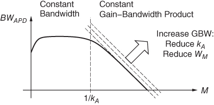
Figure 3.16 Dependence of the APD bandwidth on the DC avalanche gain.
Clearly silicon would be a better choice than InP for the multiplication layer. But getting a silicon multiplication layer to cleanly bond with an InGaAs absorption layer is a challenge [24]. Good results have been achieved by combining a silicon multiplication layer with a germanium absorption layer [27] (cf. Section 3.4). Another material that has been used successfully in high-speed APDs is indium aluminum arsenide (InAlAs or more precisely ![]() ), which has
), which has ![]() to 0.4 [24] and is lattice matched to both the InP substrate and the InGaAs absorption layer. Finally, a multiple quantum well (MQW) structure, which can be engineered to attain a low
to 0.4 [24] and is lattice matched to both the InP substrate and the InGaAs absorption layer. Finally, a multiple quantum well (MQW) structure, which can be engineered to attain a low ![]() value, can be used for the multiplication region [24]. Incidentally, the same measures that improve the APD speed (small
value, can be used for the multiplication region [24]. Incidentally, the same measures that improve the APD speed (small ![]() and small
and small ![]() ) also improve its noise characteristics, which we discuss shortly.
) also improve its noise characteristics, which we discuss shortly.
Why does the participation of only one type of carrier in the avalanche process (small ![]() ) lead to a higher APD speed? Imagine a snow avalanche coming down from a mountain. On its way down, the amount of snow (
) lead to a higher APD speed? Imagine a snow avalanche coming down from a mountain. On its way down, the amount of snow (![]() carriers) in the avalanche grows because the tumbling snow drags more snow with it. But once it's all down, the avalanche stops. Now, imagine a noisily rumbling snow avalanche that sends tremors (
carriers) in the avalanche grows because the tumbling snow drags more snow with it. But once it's all down, the avalanche stops. Now, imagine a noisily rumbling snow avalanche that sends tremors (![]() second type of carriers) back up the mountain that in turn trigger more snow avalanches coming down. This new snow brings down more snow and rumbles enough to start another mini avalanche somewhere further up the mountain. And on and on it goes. In an analogous manner, an electron-only (or hole-only) avalanche comes to an end sooner than a mixed electron–hole avalanche [1, 12].
second type of carriers) back up the mountain that in turn trigger more snow avalanches coming down. This new snow brings down more snow and rumbles enough to start another mini avalanche somewhere further up the mountain. And on and on it goes. In an analogous manner, an electron-only (or hole-only) avalanche comes to an end sooner than a mixed electron–hole avalanche [1, 12].
The equivalent AC circuit for an APD is similar to that for the p–i–n photodetector shown in Fig. 3.4, except that the current source ![]() must be replaced by a current source
must be replaced by a current source ![]() that represents the multiplied photocurrent.
that represents the multiplied photocurrent.
APDs for 10 Gb/s and Faster
Vertically illuminated APDs (cf. Fig. 3.13) are in widespread use for receivers up to and including ![]() . However, at
. However, at ![]() and beyond, the necessary thin absorption layer results in a low quantum efficiency (as discussed for the p–i–n photodetector) and edge-coupled APDs become preferable. Besides very thin absorption and multiplication regions, high-speed APDs also employ low-
and beyond, the necessary thin absorption layer results in a low quantum efficiency (as discussed for the p–i–n photodetector) and edge-coupled APDs become preferable. Besides very thin absorption and multiplication regions, high-speed APDs also employ low-![]() materials in their multiplication region.
materials in their multiplication region.
For example, the 10-Gb/s InGaAs/InAlAs waveguide APD reported in [28] achieves a bandwidth of ![]() when biased for a DC avalanche gain of 10, thus achieving a gain-bandwidth product of
when biased for a DC avalanche gain of 10, thus achieving a gain-bandwidth product of ![]() . The InGaAs absorption layer and the InAlAs multiplication layer both are
. The InGaAs absorption layer and the InAlAs multiplication layer both are ![]() thick. The Ge/Si APD reported in [27] achieves a bandwidth of
thick. The Ge/Si APD reported in [27] achieves a bandwidth of ![]() and a gain-bandwidth product of
and a gain-bandwidth product of ![]() using a 1-
using a 1-![]() thick Ge absorption layer and a 0.5-
thick Ge absorption layer and a 0.5-![]() thick Si multiplication layer.
thick Si multiplication layer.
The InGaAs/InAlAs waveguide APD reported in [29] achieves a bandwidth of ![]() when biased for a DC avalanche gain of 6 and a gain-bandwidth product of
when biased for a DC avalanche gain of 6 and a gain-bandwidth product of ![]() at around
at around ![]() , making it marginally suitable for 40-Gb/s applications. The InGaAs absorption layer of this APD is
, making it marginally suitable for 40-Gb/s applications. The InGaAs absorption layer of this APD is ![]() and the InAlAs multiplication layer is
and the InAlAs multiplication layer is ![]() thick. A similar device with a bandwidth of 30 to
thick. A similar device with a bandwidth of 30 to ![]() at a DC avalanche gain of 2 to 3 and a gain-bandwidth product of 130 to
at a DC avalanche gain of 2 to 3 and a gain-bandwidth product of 130 to ![]() , was successfully incorporated into a high-sensitivity 40-Gb/s receiver [30].
, was successfully incorporated into a high-sensitivity 40-Gb/s receiver [30].
With APDs running out of steam at about ![]() , optically preamplified p–i–n detectors, which we discuss in Section 3.3, take over. These detectors are more expensive than APDs but feature superior speed and noise performance.
, optically preamplified p–i–n detectors, which we discuss in Section 3.3, take over. These detectors are more expensive than APDs but feature superior speed and noise performance.
Avalanche Noise
Unfortunately, the APD not only provides a stronger signal but also more noise than the p–i–n photodetector, in fact, more noise than simply the amplified shot noise that we are already familiar with. At a microscopic level, each primary carrier created by a photon is multiplied by a random gain factor: for example, the first photon ends up producing nine electron–hole pairs, the next one 13, and so on. The avalanche gain ![]() , introduced earlier, is really just the average gain value.
, introduced earlier, is really just the average gain value.
The mean-square noise current of an APD illuminated by a noise-free (coherent) continuous-wave source can be written as [1, 12, 24]
where ![]() is the so-called excess noise factor and
is the so-called excess noise factor and ![]() is the primary photodetector current, that is, the current before avalanche multiplication (
is the primary photodetector current, that is, the current before avalanche multiplication (![]() ). Equivalently,
). Equivalently, ![]() can be understood as the current produced in a p–i–n photodetector with a matching responsivity
can be understood as the current produced in a p–i–n photodetector with a matching responsivity ![]() that receives the same amount of light as the APD under discussion. In the ideal case, the excess noise factor is one (
that receives the same amount of light as the APD under discussion. In the ideal case, the excess noise factor is one (![]() ), which corresponds to the situation of deterministically amplified shot noise. For a practical InGaAs/InP APD, the excess noise factor is more typically around
), which corresponds to the situation of deterministically amplified shot noise. For a practical InGaAs/InP APD, the excess noise factor is more typically around ![]() . [
. [![]() Problem 3.5.]
Problem 3.5.]
Just like the p–i–n photodetector noise, the APD noise is signal dependent, leading to unequal noise for the zeros and ones. The noise currents for a DC-balanced NRZ signal with average power ![]() and high extinction can be found with Eq. (3.14):
and high extinction can be found with Eq. (3.14):
If incomplete extinction and the primary dark current are taken into account, ![]() .
.
As plotted in Fig. 3.14, the excess noise factor ![]() increases with increasing reverse bias, roughly tracking the avalanche gain
increases with increasing reverse bias, roughly tracking the avalanche gain ![]() . Under certain assumptions, such as a relatively thick multiplication layer,
. Under certain assumptions, such as a relatively thick multiplication layer, ![]() and
and ![]() are related as follows [1, 12, 24]:
are related as follows [1, 12, 24]:
where ![]() is the same ionization-coefficient ratio that we encountered when discussing the bandwidth. For an InGaAs/InP APD, which has a relatively large
is the same ionization-coefficient ratio that we encountered when discussing the bandwidth. For an InGaAs/InP APD, which has a relatively large ![]() , the excess noise factor increases almost proportional to
, the excess noise factor increases almost proportional to ![]() , as illustrated in Fig. 3.14; for a silicon APD of Ge/Si APD, which has a very small
, as illustrated in Fig. 3.14; for a silicon APD of Ge/Si APD, which has a very small ![]() , the excess noise factor increases much more slowly with
, the excess noise factor increases much more slowly with ![]() . Not surprisingly, an orderly one-carrier-type avalanche is less noisy than a reverberating two-carrier-type one. For very thin multiplication layers we get some unexpected help. The avalanche multiplication process becomes less random resulting in an excess noise that is lower than predicted by Eq. (3.17) [24].
. Not surprisingly, an orderly one-carrier-type avalanche is less noisy than a reverberating two-carrier-type one. For very thin multiplication layers we get some unexpected help. The avalanche multiplication process becomes less random resulting in an excess noise that is lower than predicted by Eq. (3.17) [24].
Because the avalanche gain of a given APD can be increased only at the expense of more detector noise (Eq. (3.17)), there is an optimum APD gain at which the receiver becomes most sensitive. As we'll see in Section 4.4, the value of this optimum gain depends, among other things, on the APD material (![]() ).
).
The amplitude distribution of the avalanche noise, which is important for calculating the bit-error rate of APD receivers (cf. Section 4.2), is non-Gaussian. Like the shot noise from the p–i–n photodetector, the avalanche noise has an asymmetric distribution with a steep left tail (the detector current is always positive). Unfortunately, avalanche noise is much harder to analyze than shot noise. Not only does the primary current from the detection process have a random (Poisson) distribution, but the avalanche multiplication process also has a random distribution [31]. The latter distribution depends on the number of primary carriers, ![]() , that initiate the avalanche as well as the material constant
, that initiate the avalanche as well as the material constant ![]() and is strongly non-Gaussian, especially for small values of
and is strongly non-Gaussian, especially for small values of ![]() and large values of
and large values of ![]() [32, 33]. The exact mathematical form of the gain distribution is very complex but several approximations have been found [8, 31].
[32, 33]. The exact mathematical form of the gain distribution is very complex but several approximations have been found [8, 31].
Dark Current
Just like the p–i–n photodetector, the APD also suffers from a dark current. The total dark current appearing at the APD terminals can be separated into a multiplied and an unmultiplied component [8, 34]. The multiplied dark current, ![]() , arises from the primary dark current,
, arises from the primary dark current, ![]() , which is multiplied like a signal current. The unmultiplied dark current, results from surface leakage and is not multiplied. The unmultiplied dark current is often negligible when compared with the multiplied dark current. Dark current also produces noise. Like a signal current, the primary dark current
, which is multiplied like a signal current. The unmultiplied dark current, results from surface leakage and is not multiplied. The unmultiplied dark current is often negligible when compared with the multiplied dark current. Dark current also produces noise. Like a signal current, the primary dark current ![]() produces the avalanche noise
produces the avalanche noise ![]() .
.
As we know, thermally generated dark current gets worse with increasing temperature and decreasing bandgap energy. A typical high-speed InGaAs/InP APD has a primary dark current of less than ![]() at room temperature, resulting in a total dark current of less than
at room temperature, resulting in a total dark current of less than ![]() for
for ![]() . At elevated temperatures, the total dark current can go up into the microamps.
. At elevated temperatures, the total dark current can go up into the microamps.
We can again use Eq. (3.10) to judge if a given amount of dark current is harmful. With the values ![]() and
and ![]() , we find that we are fine as long as
, we find that we are fine as long as ![]() . Most high-speed APD receivers require more signal power than this to work at an acceptable bit-error rate (cf. Section 4.4), and in this case dark current is not a concern.
. Most high-speed APD receivers require more signal power than this to work at an acceptable bit-error rate (cf. Section 4.4), and in this case dark current is not a concern.
3.3 p–i–n Detector with Optical Preamplifier
An attractive alternative to the APD in direct-detection receivers is the p–i–n detector with optical preamplifier or simply the optically preamplified p–i–n detector. Rather than amplifying the photogenerated electrons, we amplify the photons before they reach the detector. Optical amplifiers come in various types [1, 2, 12, 35, 36] and several of them have been used as preamplifiers. For example, the semiconductor optical amplifier (SOA) is small and can be integrated together with an edge-coupled p–i–n photodiode on the same substrate [37], making it an attractive candidate for an optical preamplifier. Alternatively, the erbium-doped fiber amplifier (EDFA) features high gain and low noise and operates in the important 1.55-![]() band, making it a popular choice for high-performance telecommunication receivers [38, 39].
band, making it a popular choice for high-performance telecommunication receivers [38, 39].
The EDFA was co-invented around 1987 by two teams, one at the University of Southampton in England and one at AT&T Bell Laboratories in New Jersey, and has revolutionized the field of optical communication. The EDFA provides high gain over a huge bandwidth, eliminating the gain-bandwidth trade-off known from APDs. The overall detector bandwidth is limited only by the p–i–n photodetector, which can be made very large. Furthermore, the EDFA-preamplified p–i–n detector has superior noise characteristics when compared with an APD. The downsides of the EDFA are mainly its large size and high cost. In the following, we discuss the EDFA-preamplified p–i–n detector in more detail.
Erbium-Doped Fiber Amplifier
Figure 3.17 shows the operating principle of an EDFA-preamplified p–i–n detector. A WDM coupler combines the received weak optical signal with the light from a strong continuous-wave laser, known as the pump laser. The pump laser typically provides a power of about ![]() at either the 1.48-
at either the 1.48-![]() or 0.98-
or 0.98-![]() wavelength (the 0.98-
wavelength (the 0.98-![]() wavelength is preferred for low-noise preamplifiers), whereas the received signal is at the 1.55-
wavelength is preferred for low-noise preamplifiers), whereas the received signal is at the 1.55-![]() wavelength. The signal and the pump light are sent through an erbium-doped fiber, typically 10 to
wavelength. The signal and the pump light are sent through an erbium-doped fiber, typically 10 to ![]() long, where the amplification takes place. An optical isolator prevents reflections of the optical signal from entering back into the amplifier, which could cause instability and extra noise. An optical filter with bandwidth
long, where the amplification takes place. An optical isolator prevents reflections of the optical signal from entering back into the amplifier, which could cause instability and extra noise. An optical filter with bandwidth ![]() reduces the optical noise of the amplified signal before it is converted to an electrical signal with a p–i–n photodetector. (We discuss the effect of the optical filter on the electrical noise shortly.)
reduces the optical noise of the amplified signal before it is converted to an electrical signal with a p–i–n photodetector. (We discuss the effect of the optical filter on the electrical noise shortly.)
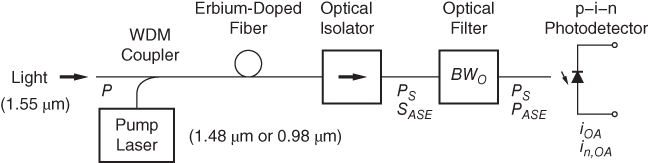
Figure 3.17 A p–i–n photodetector with erbium-doped fiber preamplifier.
The light amplification in the erbium-doped fiber can be explained as follows (see Fig. 3.18). The pump light is absorbed by the erbium ions (Er![]() ) elevating them into an excited state. In their excitement they almost radiate a photon with a wavelength around
) elevating them into an excited state. In their excitement they almost radiate a photon with a wavelength around ![]() , but they need a little encouragement from an incident photon. When that happens, the radiated photon, being a fashion-conscious boson, travels in the same direction, has the same wavelength, the same phase, the same polarization, and carries the same style hand bag as the incident photon. This process is known as stimulated emission. The radiated photon can stimulate the emission of further photons, and so forth, creating an avalanche of perfectly identical and coherent photons. At the end of the erbium-doped fiber, the optical signal is amplified, while much of the pump power is used up.
, but they need a little encouragement from an incident photon. When that happens, the radiated photon, being a fashion-conscious boson, travels in the same direction, has the same wavelength, the same phase, the same polarization, and carries the same style hand bag as the incident photon. This process is known as stimulated emission. The radiated photon can stimulate the emission of further photons, and so forth, creating an avalanche of perfectly identical and coherent photons. At the end of the erbium-doped fiber, the optical signal is amplified, while much of the pump power is used up.

Figure 3.18 Pumping and stimulated emission: (a) space–time diagram and (b) energy diagram.
Occasionally, it happens that one of the excited erbium ions cannot wait and radiates a photon even without stimulation. The resulting photon has a random direction, random wavelength (within the amplifier's bandwidth), random phase, and random polarization. This process is known as spontaneous emission. Unfortunately, a small fraction of these errant photons is radiated in the same direction as the signal photons and thus gets amplified just like those. The result is an optical noise called amplified spontaneous emission (ASE) noise.
The basic EDFA preamplifier shown in Fig. 3.17 can be enhanced in a number of ways [39]. The WDM coupler can be moved to the point after the gain medium, injecting the pump light backward through the erbium-doped fiber. This variation results in a different trade-off between noise and output power. The EDFA also can be structured as a two-stage amplifier, where the first stage is optimized for low noise and the second stage for high pumping efficiency. A second isolator may be placed at the input of the amplifier to avoid the ASE noise, which exits at the input and the output of the amplifier, from being reflected back into the amplifier or from entering a preceding amplifier stage. For a packaged EDFA, see Fig. 3.19.

Figure 3.19 A packaged variable-gain two-stage erbium-doped fiber amplifier with single-mode fiber pigtails for the input, output, and interstage access ( ).
).
Source: Reprinted by permission from Finisar Corporation.
Bandwidth
A typical EDFA has a wavelength bandwidth of around ![]() reaching from 1.530 to 1.565-
reaching from 1.530 to 1.565-![]() , corresponding to a frequency bandwidth of over
, corresponding to a frequency bandwidth of over ![]() . This is more bandwidth than that of the fastest p–i–n detectors and we do not need to worry about the bandwidth limitations introduced by the EDFA. In practice, the amplifier bandwidth is artificially reduced to
. This is more bandwidth than that of the fastest p–i–n detectors and we do not need to worry about the bandwidth limitations introduced by the EDFA. In practice, the amplifier bandwidth is artificially reduced to ![]() with an optical filter to minimize the optical output noise.
with an optical filter to minimize the optical output noise.
Where does this huge bandwidth come from? The bandwidth depends on the available energy differences, ![]() , between the excited and ground state of the erbium ions. After all, the wavelength of the emitted photon
, between the excited and ground state of the erbium ions. After all, the wavelength of the emitted photon ![]() must satisfy
must satisfy ![]() . For a theoretical two-state system (excited and ground state), there would be only a single energy difference, resulting in a very narrow amplifier bandwidth. However for erbium ions embedded in silica glass, the two energy states broaden into two energy bands, resulting in a range of energy differences and thus a much wider bandwidth (see Fig. 3.18(b)) [1, 39]. The amplifier response can be broadened and flattened further by adding dopants besides the erbium (codopants).
. For a theoretical two-state system (excited and ground state), there would be only a single energy difference, resulting in a very narrow amplifier bandwidth. However for erbium ions embedded in silica glass, the two energy states broaden into two energy bands, resulting in a range of energy differences and thus a much wider bandwidth (see Fig. 3.18(b)) [1, 39]. The amplifier response can be broadened and flattened further by adding dopants besides the erbium (codopants).
Responsivity
The power gain, ![]() , of an optical amplifier is the ratio of the output signal power (
, of an optical amplifier is the ratio of the output signal power (![]() ) to the input signal power (
) to the input signal power (![]() ). The gain of an EDFA is typically in the range
). The gain of an EDFA is typically in the range ![]() to 1,000, corresponding to 10 to
to 1,000, corresponding to 10 to ![]() . The current generated by the p–i–n photodetector,
. The current generated by the p–i–n photodetector, ![]() , expressed as a function of the optical power at the input of the preamplifier,
, expressed as a function of the optical power at the input of the preamplifier, ![]() , is
, is
where ![]() is the responsivity of the p–i–n photodetector. For
is the responsivity of the p–i–n photodetector. For ![]() and
and ![]() , the total responsivity of the preamplified p–i–n detector becomes an impressive
, the total responsivity of the preamplified p–i–n detector becomes an impressive ![]() . Whereas the APD improved the responsivity by about one order of magnitude (
. Whereas the APD improved the responsivity by about one order of magnitude (![]() ), the optically preamplified p–i–n detector can improve the responsivity by about two orders of magnitude (
), the optically preamplified p–i–n detector can improve the responsivity by about two orders of magnitude (![]() ) relative to an unaided p–i–n photodetector.
) relative to an unaided p–i–n photodetector.
The gain of an EDFA depends among other things on the pump power and the length of the erbium-doped fiber. A higher pump power results in more erbium ions being in the excited state. To obtain a gain larger than one, the rate of stimulated emissions must exceed the rate of absorptions. This point is reached when more than about 50% of the erbium ions are in the excited state and is known as population inversion. Figure 3.20 shows how the gain increases with pump power and eventually saturates when almost all erbium ions are in their excited state. A longer fiber permits the photon avalanche to grow larger, but when most of the pump power is used up, the percentage of excited erbium ions falls below 50% and the erbium-doped fiber turns into an attenuator. Thus for a given pump power there is an optimum fiber length.

Figure 3.20 EDFA gain and noise figure as a function of the pump power (normalized to the power necessary for population inversion) [1].
Because the gain depends sensitively on the pump power, EDFA modules typically incorporate a microcontroller, which adjusts the power of the pump laser based on feedback. The EDFA also can perform automatic gain control (AGC) in the optical domain [40]. To that end, a small amount of light is split off from the amplified output signal and the pump power is controlled such that the average power of this light sample remains constant.
ASE Noise
As we said earlier, the EDFA not only amplifies the desired input signal, but also produces an optical noise known as ASE noise. The PSD of this noise, ![]() , is nearly white across the huge bandwidth of the EDFA.3 Thus, we can calculate the optical noise power that reaches the photodetector as
, is nearly white across the huge bandwidth of the EDFA.3 Thus, we can calculate the optical noise power that reaches the photodetector as ![]() , where
, where ![]() is the (noise) bandwidth of the optical filter in front of the p–i–n detector. Clearly, to keep
is the (noise) bandwidth of the optical filter in front of the p–i–n detector. Clearly, to keep ![]() low, we want to use a narrow optical filter.
low, we want to use a narrow optical filter.
How does the photodetector convert this optical noise into an electrical noise? If you thought that it was odd that optical signal power is converted to a proportional electrical signal current, wait until you hear this: because the photodetector responds to the intensity, which is proportional to the square of the optical field, the optical noise gets converted into two electrical beat-noise components. Roughly speaking, we get the terms corresponding to the expansion ![]() . The first term is the desired electrical signal, the second term is known as the signal–spontaneous beat noise, and the third term is known as the spontaneous–spontaneous beat noise. A detailed analysis reveals the two electrical noise terms as [1, 41, 42]
. The first term is the desired electrical signal, the second term is known as the signal–spontaneous beat noise, and the third term is known as the spontaneous–spontaneous beat noise. A detailed analysis reveals the two electrical noise terms as [1, 41, 42]
where ![]() is the optical signal power incident on the p–i–n detector (
is the optical signal power incident on the p–i–n detector (![]() ). Furthermore, it is assumed that
). Furthermore, it is assumed that ![]() , that the optical-filter loss is negligible, and that no polarization filter is used between the amplifier and the p–i–n detector.4
, that the optical-filter loss is negligible, and that no polarization filter is used between the amplifier and the p–i–n detector.4
The first term of Eq. (3.19), the signal–spontaneous beat noise, usually is the dominant term. This noise component is proportional to the signal power ![]() (and thus also to
(and thus also to ![]() ). Note that a signal-independent optical noise density
). Note that a signal-independent optical noise density ![]() generates a signal-dependent noise term in the electrical domain! Furthermore, this noise term is not affected by the optical filter bandwidth
generates a signal-dependent noise term in the electrical domain! Furthermore, this noise term is not affected by the optical filter bandwidth ![]() , but the electrical bandwidth
, but the electrical bandwidth ![]() does matter. The second term of Eq. (3.19), the spontaneous–spontaneous beat noise, may be closer to your expectations. Similar to the signal component, this noise current component is proportional to the optical noise power. Moreover, the optical filter bandwidth does have a limiting effect on the spontaneous–spontaneous beat noise component.
does matter. The second term of Eq. (3.19), the spontaneous–spontaneous beat noise, may be closer to your expectations. Similar to the signal component, this noise current component is proportional to the optical noise power. Moreover, the optical filter bandwidth does have a limiting effect on the spontaneous–spontaneous beat noise component.
In addition to the ASE noise in Eq (3.19), optically preamplified p–i–n detectors also produce shot noise and possibly multipath interference noise. For high-gain amplifiers, the shot noise component is small and usually can be neglected (cf. Eq. (I.4)). Multipath interference (MPI) noise occurs in amplifiers with spurious reflections (e.g., from the WDM coupler, isolator, or fiber ends). The reflected waves interfere with the signal wave producing an undesirable intensity noise that depends on the phase noise in the signal [43]. [![]() Problem 3.6.]
Problem 3.6.]
SNR and OSNR
Let us calculate the electrical signal-to-noise ratio (SNR) of the optically preamplified p–i–n detector. For an optical continuous-wave signal with power ![]() and ASE noise power
and ASE noise power ![]() incident on the photodetector, the electrical signal power is
incident on the photodetector, the electrical signal power is ![]() and the electrical noise power,
and the electrical noise power, ![]() , is given by Eq. (3.19) with
, is given by Eq. (3.19) with ![]() . Dividing
. Dividing ![]() by
by ![]() yields
yields

The ratio ![]() in this equation is known as the optical signal-to-noise ratio (OSNR) measured in the optical bandwidth
in this equation is known as the optical signal-to-noise ratio (OSNR) measured in the optical bandwidth ![]() at the output of the EDFA. If the OSNR is much larger than
at the output of the EDFA. If the OSNR is much larger than ![]() (or
(or ![]() ), we can neglect the
), we can neglect the ![]() in the denominator, which is due to the spontaneous–spontaneous beat noise, and we end up with the surprisingly simple result [1, 44]
in the denominator, which is due to the spontaneous–spontaneous beat noise, and we end up with the surprisingly simple result [1, 44]

For example, for a receiver with ![]() , an OSNR of
, an OSNR of ![]() measured in a 0.1-nm bandwidth (
measured in a 0.1-nm bandwidth (![]() at
at ![]() ) translates into an electrical SNR of
) translates into an electrical SNR of ![]() . Incidentally, the result in Eq. (3.21), which we derived for a continuous-wave signal, also holds for an (ideal) NRZ-modulated signal. In Section 4.6, we use this result to analyze optically amplified transmission systems. [
. Incidentally, the result in Eq. (3.21), which we derived for a continuous-wave signal, also holds for an (ideal) NRZ-modulated signal. In Section 4.6, we use this result to analyze optically amplified transmission systems. [![]() Problem 3.7.]
Problem 3.7.]
Noise Distribution
Although the amplitude distribution of the ASE noise in the optical domain (optical field) is Gaussian, the distribution of the ASE beat noise in the electrical domain is non-Gaussian [45]. In particular, when the optical power ![]() is small, resulting in mostly spontaneous–spontaneous beat noise, the current distribution is strongly asymmetric and non-Gaussian. When the optical power is increased, making the signal–spontaneous beat noise dominant, the distribution becomes more Gaussian [46]. Figure 3.21 illustrates the distribution (probability density functions, PDF) of the p–i–n detector current for the case of a weak and strong optical signal. Note that the total detector current (signal + noise) must be positive, explaining the asymmetric shapes.
is small, resulting in mostly spontaneous–spontaneous beat noise, the current distribution is strongly asymmetric and non-Gaussian. When the optical power is increased, making the signal–spontaneous beat noise dominant, the distribution becomes more Gaussian [46]. Figure 3.21 illustrates the distribution (probability density functions, PDF) of the p–i–n detector current for the case of a weak and strong optical signal. Note that the total detector current (signal + noise) must be positive, explaining the asymmetric shapes.

Figure 3.21 Distribution of the p–i–n detector current for a weak and strong optical signal with ASE noise (from an optical amplifier).
The electrical ASE beat-noise can be described well by the non-central chi-square distribution [45, 47]. Given ![]() independent random variables
independent random variables ![]() with a Gaussian distribution (and unit variance), the random variable
with a Gaussian distribution (and unit variance), the random variable ![]() has a chi-square distribution with
has a chi-square distribution with ![]() degrees of freedom (the chi-square distribution is central if the mean of the Gaussian is zero and non-central if it is nonzero) [48]. The degree of freedom of the electrical beat-noise distribution is determined by the ratio of the optical to electrical bandwidth:
degrees of freedom (the chi-square distribution is central if the mean of the Gaussian is zero and non-central if it is nonzero) [48]. The degree of freedom of the electrical beat-noise distribution is determined by the ratio of the optical to electrical bandwidth: ![]() (for unpolarized noise). The chi-square distribution is particularly non-Gaussian for small values of
(for unpolarized noise). The chi-square distribution is particularly non-Gaussian for small values of ![]() . (The related Rayleigh and Rician distributions describe the random variable
. (The related Rayleigh and Rician distributions describe the random variable ![]() for
for ![]() when the mean of the Gaussian is zero and nonzero, respectively [48].)
when the mean of the Gaussian is zero and nonzero, respectively [48].)
Noise Figure of an Optical Amplifier
Just like electrical amplifiers, optical amplifiers are characterized by a noise figure ![]() . Typical values for an EDFA noise figure are 4 to
. Typical values for an EDFA noise figure are 4 to ![]() (see Fig. 3.20). But how is the noise figure of an optical amplifier defined?
(see Fig. 3.20). But how is the noise figure of an optical amplifier defined?
In an electrical system, the noise figure is defined as the ratio of the “total output noise power” to the “fraction of the output noise power due to the thermal noise of the source resistance.” Usually, this source resistance is ![]() . Now, an optical amplifier doesn't get its signal from a 50-
. Now, an optical amplifier doesn't get its signal from a 50-![]() source, and so the definition of its noise figure cannot be based on thermal 50-
source, and so the definition of its noise figure cannot be based on thermal 50-![]() noise. What fundamental noise is it based on? The quantum (shot) noise of the optical source!
noise. What fundamental noise is it based on? The quantum (shot) noise of the optical source!
The noise figure of an optical amplifier is defined as the ratio of the “total output noise power” to the “fraction of the output noise power due to the quantum (shot) noise of the optical source.” The output noise power is measured with a perfectly efficient p–i–n photodetector (![]() ) and is quantified as the detector's mean-square noise current.5 If we write the total output noise power as
) and is quantified as the detector's mean-square noise current.5 If we write the total output noise power as ![]() and the fraction that is due to the source as
and the fraction that is due to the source as ![]() , then the noise figure is
, then the noise figure is ![]() .
.
Figure 3.22 illustrates the various noise quantities introduced earlier. In Fig. 3.22(a), an ideal photodetector is illuminated directly by a noise-free (coherent) continuous-wave source and produces the DC current ![]() and the mean-square shot-noise current
and the mean-square shot-noise current ![]() . In Fig. 3.22(b), the signal from the same optical source is amplified with a noiseless, deterministic amplifier with gain
. In Fig. 3.22(b), the signal from the same optical source is amplified with a noiseless, deterministic amplifier with gain ![]() . This amplifier multiplies every photon from the source into exactly
. This amplifier multiplies every photon from the source into exactly ![]() photons. The ideal photodetector now produces the DC current
photons. The ideal photodetector now produces the DC current ![]() and the mean-square shot-noise current
and the mean-square shot-noise current ![]() (cf. Problem 3.5). Note that this quantity represents the “output noise power due to the quantum (shot) noise of the optical source.” In Fig. 3.22(c), we replaced the noiseless amplifier with a real amplifier with gain
(cf. Problem 3.5). Note that this quantity represents the “output noise power due to the quantum (shot) noise of the optical source.” In Fig. 3.22(c), we replaced the noiseless amplifier with a real amplifier with gain ![]() and noise figure
and noise figure ![]() . According to the noise figure definition, the ideal photodetector now produces a mean-square noise current that is
. According to the noise figure definition, the ideal photodetector now produces a mean-square noise current that is ![]() times larger than in Fig. 3.22(b):
times larger than in Fig. 3.22(b):
where ![]() is the current produced by an ideal photodetector receiving the same amount of light as the optical preamplifier (cf. Fig. 3.22(a)).
is the current produced by an ideal photodetector receiving the same amount of light as the optical preamplifier (cf. Fig. 3.22(a)).

Figure 3.22 Definition of the noise figure for an optical amplifier: (a) source noise, (b) output noise due to the source, and (c) total output noise.
With the definition of the noise figure in hand, we can now write the noise current of an optically preamplified p–i–n detector with preamplifier gain ![]() , noise figure
, noise figure ![]() , and p–i–n detector quantum efficiency
, and p–i–n detector quantum efficiency ![]() . This noise current is almost given by Eq. (3.22), except that the latter equation assumes an ideal detector with
. This noise current is almost given by Eq. (3.22), except that the latter equation assumes an ideal detector with ![]() . To take the reduced quantum efficiency of a real detector into account, we have to multiply
. To take the reduced quantum efficiency of a real detector into account, we have to multiply ![]() in Eq. (3.22) by
in Eq. (3.22) by ![]() and replace the ideal
and replace the ideal ![]() in Eq. (3.22) by
in Eq. (3.22) by ![]() . The resulting mean-square noise current is
. The resulting mean-square noise current is
where ![]() is the current produced by the real p–i–n photodetector receiving the same amount of light as the optical preamplifier.
is the current produced by the real p–i–n photodetector receiving the same amount of light as the optical preamplifier.
Like for the unamplified p–i–n photodetector and the APD, the noise of the optically preamplified p–i–n detector is signal power dependent and therefore the noise current for zeros and ones is different. Given a DC-balanced NRZ signal with average power ![]() and high extinction, we find with Eq. (3.23):
and high extinction, we find with Eq. (3.23):
If incomplete extinction, spontaneous–spontaneous beat noise, and dark current are taken into account, ![]() .
.
If we compare the noise expression Eq. (3.14) for the APD with Eq. (3.23) for the optically preamplified p–i–n detector, we find that the excess noise factor ![]() of the APD plays the same role as the product
of the APD plays the same role as the product ![]() of the optically preamplified p–i–n detector.
of the optically preamplified p–i–n detector.
Noise Figure and ASE Noise
In Eq. (3.19), we expressed the electrical noise in terms of the optical ASE noise and in Eq. (3.23), we expressed the electrical noise in terms of the amplifier's noise figure. Now let us combine the two equations and find out how the noise figure is related to the ASE noise. Solving Eq. (3.23) for ![]() and using Eqs. (3.19) and (3.3), we find
and using Eqs. (3.19) and (3.3), we find

The first term is due to the signal–spontaneous beat noise, and the second term is due to the spontaneous–spontaneous beat noise. Note that this noise figure depends on the input power ![]() and becomes infinite for
and becomes infinite for ![]() . The reason for this behavior is that when the signal power goes to zero, we are still left with the spontaneous–spontaneous beat noise, whereas the quantum (shot) noise due to the source does go to zero. Equation (3.26) can be extended to include shot noise terms (cf. Eq. (I.5)), but for a gain much larger than one, these terms are very small. [
. The reason for this behavior is that when the signal power goes to zero, we are still left with the spontaneous–spontaneous beat noise, whereas the quantum (shot) noise due to the source does go to zero. Equation (3.26) can be extended to include shot noise terms (cf. Eq. (I.5)), but for a gain much larger than one, these terms are very small. [![]() Problem 3.8.]
Problem 3.8.]
Sometimes it is convenient to define another type of noise figure ![]() that corresponds to just the first term of Eq. (3.26) [42]:
that corresponds to just the first term of Eq. (3.26) [42]:
This noise figure is known as the signal–spontaneous beat noise limited noise figure [43] or the optical noise figure.6 It has the advantages of being easier to measure [43] and being independent of the input power. For an OSNR much larger than ![]() and a gain much larger than
and a gain much larger than ![]() , the two noise figures become approximately equal. Nevertheless, the fact that there are two similar but not identical noise figure definitions can be a source of confusion.
, the two noise figures become approximately equal. Nevertheless, the fact that there are two similar but not identical noise figure definitions can be a source of confusion.
A detailed analysis of the ASE noise physics reveals the following expression for its PSD [1, 36, 43]:

where ![]() is the number of erbium ions in the ground state and
is the number of erbium ions in the ground state and ![]() is the number of erbium ions in the excited state. The stronger the amplifier is “pumped,” the more erbium ions are in the excited state. Thus for a strongly pumped amplifier, we have
is the number of erbium ions in the excited state. The stronger the amplifier is “pumped,” the more erbium ions are in the excited state. Thus for a strongly pumped amplifier, we have ![]() (full population inversion). Combining Eq. (3.27) for the optical noise figure with Eq. (3.28) and assuming
(full population inversion). Combining Eq. (3.27) for the optical noise figure with Eq. (3.28) and assuming ![]() , we find the following simple approximation for the EDFA noise figure(s) [1, 36, 39]:
, we find the following simple approximation for the EDFA noise figure(s) [1, 36, 39]:

This equation implies that increasing the pump power decreases the noise figure until it bottoms out at the theoretical limit ![]() (or
(or ![]() ), in agreement with the plot in Fig. 3.20.
), in agreement with the plot in Fig. 3.20.
Fiber Optical Parametric Amplifier and Noise Figures Below 3 dB
Why is the minimum noise figure of an EDFA two and not one? An amplifier with ![]() does not require that there is zero ASE noise (
does not require that there is zero ASE noise (![]() ), which would be quite impossible, but only that the ASE noise equals the amplified quantum (shot) noise. So,
), which would be quite impossible, but only that the ASE noise equals the amplified quantum (shot) noise. So, ![]() does not seem totally impossible.
does not seem totally impossible.
Is this a flaw of the EDFA? No, it is a fundamental limit for phase-insensitive amplifiers dictated by the uncertainty principle [49]. An amplifier with high gain and ![]() would permit us to amplify the optical field from the quantum domain to the classical domain and measure the in-phase and quadrature components of the field accurately and simultaneously, in violation of the uncertainty principle [50].
would permit us to amplify the optical field from the quantum domain to the classical domain and measure the in-phase and quadrature components of the field accurately and simultaneously, in violation of the uncertainty principle [50].
An OOK receiver does not rely on phase information and an optical amplifier that amplifies the in-phase component but suppresses the quadrature component, a so-called phase-sensitive amplifier, is sufficient. Now, such an amplifier can reach ![]() , because it does not bring the phase information into the classical domain. Interestingly, the fiber optical parametric amplifier (FOPA) can be configured such that it amplifies only the field component that is phase aligned with the pump field [49]. Phase-sensitive FOPAs with sub-3-dB noise figures have been demonstrated in the lab.
, because it does not bring the phase information into the classical domain. Interestingly, the fiber optical parametric amplifier (FOPA) can be configured such that it amplifies only the field component that is phase aligned with the pump field [49]. Phase-sensitive FOPAs with sub-3-dB noise figures have been demonstrated in the lab.
Raman Amplifier and Negative Noise Figures
We conclude this section with a brief look at the Raman amplifier and its noise figure. This amplifier is named after the Indian physicist Chandrasekhara Venkata Raman, who discovered the Raman effect and was awarded the Nobel Prize in 1930. Raman amplification in optical fiber was first observed and measured in the early 1970s (Roger Stolen and Erich Ippen).
Figure 3.23(a) shows the basic distributed Raman amplifier [51, 52]. Unlike an EDFA, which provides gain at the point where the amplifier is located, this amplifier provides distributed gain in the transmission fiber itself. The fiber span is pumped from the receiver end with a strong laser (![]() or so) at a frequency that is about
or so) at a frequency that is about ![]() above (
above (![]() below) the signal to be amplified. The signal-power profile depicted in Fig. 3.23(b) shows that most of the amplification occurs in the last
below) the signal to be amplified. The signal-power profile depicted in Fig. 3.23(b) shows that most of the amplification occurs in the last ![]() of the span where the pump power is highest. In our example, the 100-km span has a loss of
of the span where the pump power is highest. In our example, the 100-km span has a loss of ![]() when the Raman pump is off. This loss reduces to
when the Raman pump is off. This loss reduces to ![]() when the Raman pump is on, thus providing an on/off gain of
when the Raman pump is on, thus providing an on/off gain of ![]() .
.
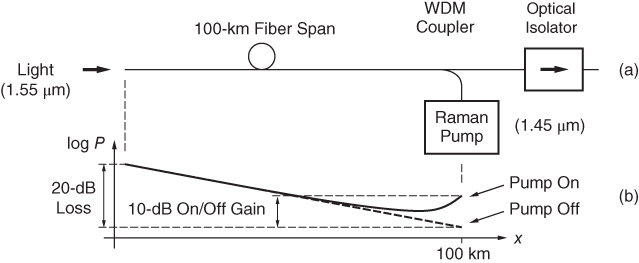
Figure 3.23 Distributed Raman amplifier: (a) structure and (b) signal-power profile.
The Raman amplification in the transmission fiber can be explained as follows. Stimulated by the incident signal photons, some of the pump photons “decay” into a (lower-energy) signal photon and a molecular vibration (a phonon) as illustrated in Fig. 3.24. Like in the EDFA, the resulting signal photon is coherent to the stimulating one, thus amplifying the signal. This process is known as stimulated Raman scattering (cf. Section 2.3). The available vibrational (phonon) energy states in silica glass range from about ![]() to
to ![]() (see Fig. 3.24(b)), resulting in a huge amplifier bandwidth of about
(see Fig. 3.24(b)), resulting in a huge amplifier bandwidth of about ![]() . This bandwidth can be made even larger by using multiple pump lasers with different wavelengths [53].
. This bandwidth can be made even larger by using multiple pump lasers with different wavelengths [53].
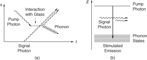
Figure 3.24 Stimulated Raman scattering: (a) space–time diagram and (b) energy diagram.
How large is the noise figure of a Raman amplifier? To answer this question, let us compare a fiber span followed by an EDFA with the same fiber span followed by a Raman pump. A fiber span with loss ![]() or gain
or gain ![]() , where
, where ![]() , has a noise figure of
, has a noise figure of ![]() . The same fiber span followed by a lumped optical amplifier with noise figure
. The same fiber span followed by a lumped optical amplifier with noise figure ![]() has a combined noise figure of
has a combined noise figure of ![]() (cf. Eq. (I.6)). Both facts can be proven with the noise-figure definition given earlier. For example, our 100-
(cf. Eq. (I.6)). Both facts can be proven with the noise-figure definition given earlier. For example, our 100-![]() fiber span with 20-
fiber span with 20-![]() loss followed by an EDFA with a noise figure of
loss followed by an EDFA with a noise figure of ![]() has a total noise figure of
has a total noise figure of ![]() . [
. [![]() Problem 3.9.]
Problem 3.9.]
Now let us replace the EDFA with a Raman pump. With the pump off, the noise figure is ![]() , equal to the loss. With the pump on, the loss reduces to
, equal to the loss. With the pump on, the loss reduces to ![]() and ideally the noise figure also should reduce to
and ideally the noise figure also should reduce to ![]() . But just like the EDFA, the Raman amplifier generates ASE noise and the actual noise figure is worse than that; let us say, it is
. But just like the EDFA, the Raman amplifier generates ASE noise and the actual noise figure is worse than that; let us say, it is ![]() . Now, comparing the distributed Raman amplifier with the lumped EDFA amplifier, it becomes evident that the former behaves like the latter with an effective noise figure of
. Now, comparing the distributed Raman amplifier with the lumped EDFA amplifier, it becomes evident that the former behaves like the latter with an effective noise figure of ![]() . Distributed Raman amplifiers can achieve negative noise figures, at least in a differential sense!
. Distributed Raman amplifiers can achieve negative noise figures, at least in a differential sense!
Raman amplifiers are of great practical significance, especially when used as in-line amplifiers in ultra-long-haul transmission systems. Their distributed gain permits roughly a doubling of the span length when compared to an EDFA-only solution (e.g., from 40 to ![]() ) [54], cutting the number of optical amplifiers needed in half. Moreover, the bandwidth of an advanced Raman amplifier (with multiple pump wavelengths) is about twice that of an EDFA (
) [54], cutting the number of optical amplifiers needed in half. Moreover, the bandwidth of an advanced Raman amplifier (with multiple pump wavelengths) is about twice that of an EDFA (![]() vs
vs ![]() ) [54], permitting a doubling of the number of WDM channels.
) [54], permitting a doubling of the number of WDM channels.
3.4 Integrated Photodetectors
Optoelectronic Integration
The speed and noise performance of a receiver depends critically on the total capacitance at its input node (cf. Chapter 6). The bonding pads, ESD protection circuits, and the TIA and photodetector packages all contribute to this capacitance. Bringing the photodetector as close as possible to the TIA and avoiding separate packages has the benefit of reducing this capacitance. In addition, such an integration results in a more compact system, potentially reducing the cost and improving the reliability. The photodetector and the TIA circuit can be integrated in a number of different ways:
- Detector and circuit chip in the same package. For high-speed optical receivers, it is common practice to copackage the photodetector and the TIA into a receiver optical subassembly (ROSA), usually in the form of a small coaxial module (cf. Fig. 1.3). Similarly, a photonic integrated circuit (PIC) containing the photodiodes and a coherent receiver front-end [55, 56] can be copackaged with the TIA chips into a multi-chip module (MCM). A digital processor chip may be copackaged with an array of photodetectors and lasers (VCSELs) into an MCM to form a high-performance processor module with optical inputs and outputs [57]. This method of integration permits the technology for the photodetectors and the technology for the circuit chip to be chosen and optimized independently. For example, the photodetector can be based on an InP substrate, whereas the TIA circuit is implemented in a standard silicon technology.
- Detector chip mounted on the circuit chip. Pushing the integration one step further, the photodetector can be mounted on the circuit chip and can be connected by means of flip-chip bonding [58–62] or wire bonding [63], thus eliminating the substrate traces of the MCM. This method still permits an independent choice of the photodetector and circuit technologies, as in the previous case. For example, in [60] an array of AlGaAs p–i–n photodetectors were flip-chip bonded on a standard CMOS chip.
-
Detector and circuit monolithically integrated in an OEIC technology. The next step in integration is to put the photodetector and the receiver circuits on the same chip, resulting in a so-called optoelectronic integrated circuits (OEIC) [5, 64]. The simplest form of an OEIC is the p–i–n FET, which combines a p–i–n photodetector and an FET on the same substrate. An OEIC technology is usually based on a circuit technology. Extra fabrication steps are then added to implement good-quality photodetectors (and possibly other components such as lasers, modulators, and waveguides).
Adding photodetectors to a circuit technology involves compromises. For example, to fabricate long-wavelength (1.3 or 1.55-
 ) photodetectors in a silicon circuit technology, it is necessary to incorporate a low-bandgap material such as germanium. However, germanium layers grown on silicon are prone to defects due to a lattice mismatch of about 4% between the two materials [65]. Another problem is that the maximum temperature permitted to anneal the germanium is limited in order not to degrade the performance of the silicon devices [65]. (If the germanium is deposited on top of the circuit technology's metal stack, the maximum processing temperature is limited to about
  [57].) Yet another problem arises if the photodetector is thicker than the circuit devices (which may be necessary to obtain a decent quantum efficiency). This lack of planarity makes it difficult to contact the devices with the metal layers [65]. Even for short-wavelength (0.85-
 ) applications, where silicon can act as the absorber, incorporating fast photodetectors with high responsivity and low capacitance is challenging.
Nevertheless, the promise of compactness, high performance, low cost, and improved reliability has resulted in the development of many OEIC technologies and the design of many integrated receivers. OEICs based on InP circuit technologies [66–68], GaAs circuit technologies [69–71], bipolar or BiCMOS circuit technologies [72–76], and CMOS technologies [27, 57, 65, 77, 78] have all been reported. Of particular interest are detectors that are compatible with CMOS technology and we discuss two examples (Ge detector and Ge/Si APD) shortly.
-
Detector and circuit monolithically integrated in a standard circuit technology. Naturally, it would be simpler and more cost effective, if the photodetector could be implemented in a standard, that is, unmodified, circuit technology. Indeed, this is possible if the necessary performance compromises and wavelength restrictions are acceptable.
For example, in a standard MESFET (or HFET) technology the Schottky diode formed between the gate metal and the semiconductor can be used to implement a so-called metal–semiconductor–metal (MSM) photodetector [79]. In a standard bipolar (or HBT) technology the base–collector junction may serve as a photodiode [80]. Similarly, in a standard CMOS technology the n-well to p-substrate or the p+ (drain/source) to n-well junctions may serve as a photodiode [81]. We discuss some of these photodetectors (MSM and CMOS junctions) shortly.
CMOS Compatible Germanium Photodetector
The structure of a germanium waveguide p–i–n photodetector suitable for the 1.55-![]() wavelength and compatible with SOI-CMOS technology is illustrated in Fig. 3.25.
wavelength and compatible with SOI-CMOS technology is illustrated in Fig. 3.25.
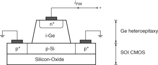
Figure 3.25 CMOS compatible germanium p–i–n photodetector [78].
Selective heteroepitaxy is used to grow the germanium detector on top of an SOI CMOS wafer. Although the 4% lattice mismatch between germanium and silicon can result in a high concentration of dislocations and dark current, careful processing and device design can minimize the impact of the dislocations.
The device described in [78] achieves a responsivity of ![]() at the 1.55-
at the 1.55-![]() wavelength and a 1-V reverse bias. The dark current at room temperature and a 1-V reverse bias is about
wavelength and a 1-V reverse bias. The dark current at room temperature and a 1-V reverse bias is about ![]() . Although this dark current is much larger than that of an InGaAs/InP photodetector, it is tolerable for coherent receivers, where typical average photocurrents are 1mA or higher [56].
. Although this dark current is much larger than that of an InGaAs/InP photodetector, it is tolerable for coherent receivers, where typical average photocurrents are 1mA or higher [56].
CMOS-Compatible Germanium/Silicon APD
The structure of a germanium/silicon APD suitable for the 1.3-![]() wavelength and compatible with CMOS technology is illustrated in Fig. 3.26.
wavelength and compatible with CMOS technology is illustrated in Fig. 3.26.

Figure 3.26 CMOS-compatible germanium/silicon APD [27].
While InP-based optoelectronic devices are often superior to silicon-based devices, one of the exceptions is the area of APDs. As we have discussed in Section 3.2, a silicon multiplication region has important advantages over an InP or InAlAs multiplication region. The lower ionization-coefficient ratio ![]() of silicon leads to a higher gain-bandwidth product and a lower noise.
of silicon leads to a higher gain-bandwidth product and a lower noise.
The Ge/Si APD reported in [27] achieves a gain-bandwidth product of ![]() . The maximum bandwidth is
. The maximum bandwidth is ![]() for gains up to 20. The effective ionization-coefficient ratio that determines the excess noise factor (cf. Eq (3.17)) is
for gains up to 20. The effective ionization-coefficient ratio that determines the excess noise factor (cf. Eq (3.17)) is ![]() . The thermal coefficient of the breakdown voltage is 0.05%/
. The thermal coefficient of the breakdown voltage is 0.05%/![]() . This low thermal coefficient (lower than that for an InP- or InAlAs-based APD) is another advantage of the Ge/Si APD.
. This low thermal coefficient (lower than that for an InP- or InAlAs-based APD) is another advantage of the Ge/Si APD.
Metal–Semiconductor–Metal Photodetector (MESFET/HFET Technology)
The MSM photodetector has the advantage that is can be implemented in an unmodified MESFET or HFET technology [79]. Nevertheless, specialized OEIC technologies also make use of this detector because of its simplicity (only one or two additional processing steps) and planarity [57, 69, 70, 73].
The operation of a basic MSM photodetector based on GaAs technology, which is suitable for the 0.85-![]() wavelength, is illustrated in Fig. 3.27. Metal in direct contact with a semiconductor forms a Schottky diode [5]. Two interdigitated metal electrodes on top of the GaAs semiconductor form two back-to-back Schottky diodes, which constitute the MSM photodetector. When a bias voltage is applied across the MSM detector one diode becomes forward biased and the other diode becomes reverse biased. Unlike for a p–i–n photodetector, the polarity of the bias voltage doesn't matter, as is obvious from the MSM structure's symmetry. Light that impinges on the exposed semiconductor between the metal electrodes creates electron–hole pairs, provided that the photon energy exceeds the bandgap energy of the semiconductor. Like in a p–i–n photodetector, the electron–hole pairs get separated by the electric field in the reverse-biased Schottky diode and produce the photocurrent
wavelength, is illustrated in Fig. 3.27. Metal in direct contact with a semiconductor forms a Schottky diode [5]. Two interdigitated metal electrodes on top of the GaAs semiconductor form two back-to-back Schottky diodes, which constitute the MSM photodetector. When a bias voltage is applied across the MSM detector one diode becomes forward biased and the other diode becomes reverse biased. Unlike for a p–i–n photodetector, the polarity of the bias voltage doesn't matter, as is obvious from the MSM structure's symmetry. Light that impinges on the exposed semiconductor between the metal electrodes creates electron–hole pairs, provided that the photon energy exceeds the bandgap energy of the semiconductor. Like in a p–i–n photodetector, the electron–hole pairs get separated by the electric field in the reverse-biased Schottky diode and produce the photocurrent ![]() .
.

Figure 3.27 MSM photodetector: (a) cross-sectional view, (b) top view (on a different scale and with more fingers), and (c) circuit symbol.
An obvious drawback of the MSM photodetector is that the light impinging on the metal is blocked and does not contribute to the photocurrent [4, 8, 82]. Thus, an MSM photodetector with an electrode width equal to the electrode spacing, as shown in Fig. 3.27, has a quantum efficiency (and responsivity) that is only about half of that of a p–i–n photodetector. Less shadowing and a better efficiency can be obtained by increasing the electrode spacing relative to the width, but this measure also increases the carrier transit time and thus reduces the bandwidth of the detector. (Moreover, too much spacing results in excessive carrier recombination and fewer carriers being picked up by the electrodes, reducing the quantum efficiency.) In principle, shadowing can be avoided by using transparent conductors, but this option requires special processing steps [4].
An advantage of the MSM photodetector is its low capacitance. For a given detector area, an MSM photodetector has only about 30% of the capacitance of a comparable p–i–n detector [82]. The reason for this reduction is that the MSM detector operates on the fringe capacitance between the metal fingers, whereas the p–i–n detector relies on the area capacitance between the p-layer and the n-layer. This lower capacitance can make up for some or all of the sensitivity lost because of the lower responsivity [82]. If low capacitance is not a priority, the area of the MSM photodetector can be made large (e.g., ![]() ) to simplify the coupling of the light from the fiber to the detector and to reduce the cost of the system [4].
) to simplify the coupling of the light from the fiber to the detector and to reduce the cost of the system [4].
The transit-time limited speed of the MSM photodetector is primarily given by the spacing between the metal fingers and the carrier velocities, which in turn are a function of the applied bias voltage. MSMs also tend to have low-field regions resulting in diffusion-limited tails. (The bandwidth calculation for an MSM is more complicated than that for a p–i–n structure because carriers generated far away from the surface see a weaker electric field, move well below the saturation velocity, and have a longer way to travel to the electrodes [83].) A bandwidth of ![]() was achieved for a small (
was achieved for a small (![]() ) GaAs MSM photodetector with a finger spacing of
) GaAs MSM photodetector with a finger spacing of ![]() [84].
[84].
The MSM photodetector can be made sensitive to long wavelengths by using a narrow-bandgap semiconductor such as germanium or InGaAs. However, the resulting lower Schottky barrier between the metal and semiconductor leads to a larger dark current. To control this dark current, a thin layer (either a lightly doped implant or an epitaxial layer of a wide-bandgap material) can be sandwiched between the absorbing semiconductor and the metal [4, 82].
CMOS N-Well to P-Substrate Photodiode
Although the bandgap of silicon is narrow enough to absorb light at the 0.85-![]() wavelength, the indirect nature of the bandgap results in a large absorption length, measuring about
wavelength, the indirect nature of the bandgap results in a large absorption length, measuring about ![]() [72]. For comparison, the absorption length of GaAs is only
[72]. For comparison, the absorption length of GaAs is only ![]() [72] and that of germanium is
[72] and that of germanium is ![]() [65] at the same 0.85-
[65] at the same 0.85-![]() wavelength. Thus, for a silicon photodetector to have a good quantum efficiency, a thick absorption layer is required, which unfortunately results in a long transit time for the photogenerated carriers.
wavelength. Thus, for a silicon photodetector to have a good quantum efficiency, a thick absorption layer is required, which unfortunately results in a long transit time for the photogenerated carriers.
When we restrict ourselves to building the photodetector in a standard CMOS technology, there are additional challenges. The junction between the lightly doped n-well and p-substrate provides the thickest depletion layer in a CMOS technology that can be used to absorb photons. A CMOS photodetector based on this junction is shown in Fig. 3.28. Even then, the thickness of the depletion layer, outlined with thin dashed lines, is only about ![]() at
at ![]() [85], far less than the absorption length. As a result, the quantum efficiency of this photodiode is limited to about 37% [85]. Even worse, the light that didn't get absorbed in the depletion layer penetrates into the substrate where it creates electron–hole pairs outside of the drift field. The resulting minority carriers diffuse around aimlessly and, if not lost to recombination, contribute to a slow current tail (cf. Section 3.1). (In a silicon on insulator [SOI] technology, the insulator below the n-well can be used to block the carriers from diffusing back into the drift field [72].)
[85], far less than the absorption length. As a result, the quantum efficiency of this photodiode is limited to about 37% [85]. Even worse, the light that didn't get absorbed in the depletion layer penetrates into the substrate where it creates electron–hole pairs outside of the drift field. The resulting minority carriers diffuse around aimlessly and, if not lost to recombination, contribute to a slow current tail (cf. Section 3.1). (In a silicon on insulator [SOI] technology, the insulator below the n-well can be used to block the carriers from diffusing back into the drift field [72].)

Figure 3.28 CMOS n-well to p-substrate photodiode: (a) cross-sectional view and (b) circuit view.
In a practical implementation of this photodetector, the single n-well region schematically shown in Fig. 3.28 is replaced by several parallel n-well stripes, which are all connected together. Such a finger layout increases the junction's side-wall depletion region [86], reduces the contact resistance [81, 87], and for small finger widths can increase the bandwidth by a small amount [81, 88].
Unfortunately, the relatively thin absorption layer is not the only factor limiting the responsivity of this CMOS photodiode. Reflection and refraction of the light in the dielectric stack above the silicon attenuates the incident light even before it has a chance to reach the photodiode [85, 89]. The dielectric stack consist of the field oxide, the dielectrics used between the metal layers, and the capping layer. This stack limits the transmission of the incident light to about 40 to 70% [89]. Combining this figure with the 37% (high-frequency) quantum efficiency mentioned before yields an overall quantum efficiency of only about 20%, which corresponds to a paltry responsivity of ![]() at the 0.85-
at the 0.85-![]() wavelength. Technology scaling makes the responsivity problem even worse: more metal layers result in a less transparent dielectric stack, increased doping levels and lower supply voltages result in a thinner and less effective depletion layer [89]. The deposition of silicide over CMOS active regions to facilitate low-resistance contacts presents another impediment. If not blocked over the photodiode, this silicide layer can absorb up to 95% of the incident light [90].
wavelength. Technology scaling makes the responsivity problem even worse: more metal layers result in a less transparent dielectric stack, increased doping levels and lower supply voltages result in a thinner and less effective depletion layer [89]. The deposition of silicide over CMOS active regions to facilitate low-resistance contacts presents another impediment. If not blocked over the photodiode, this silicide layer can absorb up to 95% of the incident light [90].
The bandwidth of the n-well/p-substrate photodiode is mostly determined by the minority carriers that are produced outside of the depletion layer, namely the holes in the n-well above and the electrons in the p-substrate below [81, 91]. Of those minority carriers, the electrons created deep in the substrate are the most troublesome. Typical bandwidth values are between 1 and 10![]() [81, 92], well below what is needed for a Gb/s optical receiver. But finally there is some good news: the frequency roll-off of the responsivity at high frequencies is relatively slow. Typical values range from
[81, 92], well below what is needed for a Gb/s optical receiver. But finally there is some good news: the frequency roll-off of the responsivity at high frequencies is relatively slow. Typical values range from ![]() to
to ![]() [81], compared with
[81], compared with ![]() for a first-order low-pass filter. This slow roll-off can be compensated quite effectively with a simple analog equalizer. Integrated 3-
for a first-order low-pass filter. This slow roll-off can be compensated quite effectively with a simple analog equalizer. Integrated 3-![]() receivers with an n-well/p-substrate photodiode followed by such an equalizer have been demonstrated [81, 87]. In [81], the equalizer, which needs to have a slow frequency “roll-up,” has been realized by summing the outputs of four frequency-staggered first-order high-pass filters.
receivers with an n-well/p-substrate photodiode followed by such an equalizer have been demonstrated [81, 87]. In [81], the equalizer, which needs to have a slow frequency “roll-up,” has been realized by summing the outputs of four frequency-staggered first-order high-pass filters.
CMOS P+ to N-Well Photodiode
Another CMOS junction suitable for photodetection is the p+ (drain or source) to n-well junction, shown in Fig. 3.29. Because the p+ material is more heavily doped than the p-substrate, the resulting depletion layer is thinner and the responsivity lower than that of the n-well/p-substrate photodiode. On the plus side, the n-well/p-substrate photodiode can now be used to collect the carriers that are generated below the p+/n-well photodiode thus removing the slow current tail from the upper photodiode [93]. Figure 3.29 illustrates how the photocurrent collected by the n-well/p-substrate photodiode is dumped to ground, whereas the photocurrent collected by the p+/n-well photodiode is fed to the TIA.
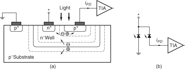
Figure 3.29 CMOS p+ to n-well photodiode: (a) cross-sectional view and (b) circuit view.
In a practical implementation, the single p+ region, schematically shown in Fig. 3.29, is replaced by several parallel p+ stripes (fingers) located in a joint n-well [93]. The advantages of this geometry are similar to those given for the n-well/p-substrate photodetector. In a deep n-well technology, where it is possible to create an isolated p-well, the structure shown in Fig. 3.29 can be “inverted” to produce an n+/p-well photodiode located inside the deep n-well [94].
The p+/n-well photodiode and the n-well/p-substrate photodiode have been compared to each other extensively [81, 92]. It has been found that the p+/n-well photodiode has a bandwidth of about 1 to ![]() , an improvement of almost three orders of magnitude over the n-well/p-substrate photodiode. However, the responsivity of the p+/n-well photodiode is about 10 to 20 times smaller than that of the n-well/p-substrate photodiode. Moreover, owing to the thinner depletion layer, the capacitance per area of the p+/n-well photodiode is about twice that of the n-well/p-substrate photodiode.
, an improvement of almost three orders of magnitude over the n-well/p-substrate photodiode. However, the responsivity of the p+/n-well photodiode is about 10 to 20 times smaller than that of the n-well/p-substrate photodiode. Moreover, owing to the thinner depletion layer, the capacitance per area of the p+/n-well photodiode is about twice that of the n-well/p-substrate photodiode.
An integrated 1-![]() receiver using a p+/n-well photodiode has been reported in [93]. The photodiode by itself has a responsivity ranging from 0.01 to
receiver using a p+/n-well photodiode has been reported in [93]. The photodiode by itself has a responsivity ranging from 0.01 to ![]() at the 0.85-
at the 0.85-![]() wavelength, where the larger value corresponds to a bias voltage near the junction breakdown (
wavelength, where the larger value corresponds to a bias voltage near the junction breakdown (![]() ). A larger reverse bias voltage increases the thickness of the depletion layer and hence the fraction of photons absorbed there. An integrated 2.5-
). A larger reverse bias voltage increases the thickness of the depletion layer and hence the fraction of photons absorbed there. An integrated 2.5-![]() receiver with a similar photodiode type biased at
receiver with a similar photodiode type biased at ![]() has been presented in [94]. Both receivers reach the stated bit rate without the use of an equalizer.
has been presented in [94]. Both receivers reach the stated bit rate without the use of an equalizer.
CMOS Spatially Modulated Light (SML) Detector
An innovative approach is taken by the spatially modulated light (SML) detector [85, 91]. This detector, which is shown schematically in Fig. 3.30, is based on the CMOS n-well/p-substrate photodiode. But instead of exposing all the n-well fingers to the light, every second finger is blocked by a layer of metal (usually layer-2 metal). All the illuminated junctions are connected together and all the dark junctions are connected together. Figure 3.30(a) shows the cross-sectional view of two such n-well/p-substrate junctions, one illuminated and one dark. The idea is that the troublesome carriers generated deep in the substrate have an approximately equal chance of diffusing to an illuminated junction or a dark junction. Thus, the slow current tail appears at both junctions and can be suppressed by subtracting the photocurrent of the dark junctions ![]() from the photocurrent of the illuminated junctions
from the photocurrent of the illuminated junctions ![]() . A differential TIA, which we discuss in Section 7.2, can be used to perform the subtraction
. A differential TIA, which we discuss in Section 7.2, can be used to perform the subtraction ![]() . The currents from the illuminated and dark junctions,
. The currents from the illuminated and dark junctions, ![]() and
and ![]() , are sometimes called the immediate and the deferred currents, respectively. Conveniently, the indices I and D permit either interpretation.
, are sometimes called the immediate and the deferred currents, respectively. Conveniently, the indices I and D permit either interpretation.
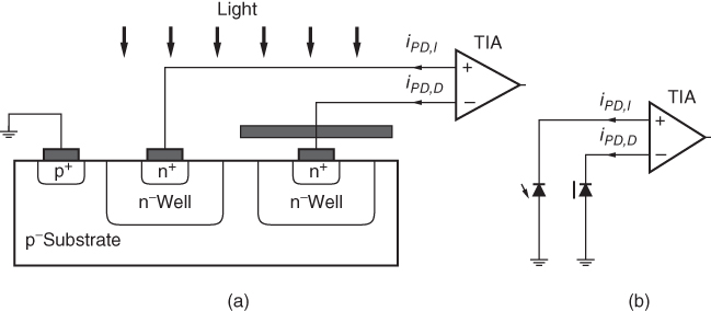
Figure 3.30 CMOS spatially modulated light detector: (a) cross-sectional view and (b) circuit view.
After the current subtraction, the bandwidth of the SML detector is typically in the range from 0.6 to ![]() [86, 88, 92], not far from that of a p+/n-well photodiode. This bandwidth is believed to increase with technology scaling because more closely spaced n-well/p-substrate photodiodes will pick up the diffusing carriers more evenly [91]. The SML detector's responsivity is typically in the range from 0.05 to
[86, 88, 92], not far from that of a p+/n-well photodiode. This bandwidth is believed to increase with technology scaling because more closely spaced n-well/p-substrate photodiodes will pick up the diffusing carriers more evenly [91]. The SML detector's responsivity is typically in the range from 0.05 to ![]() at the 0.85-
at the 0.85-![]() wavelength [86, 88, 92], better than that of a p+/n-well photodiode. The capacitance per photodiode area is similar to that of the n-well/p-substrate photodiode and lower than that of the p+/n-well photodiode. The matched photodiode capacitances combined with the fact that the signal is represented by the difference of two currents results in a superior noise immunity (cf. Section 7.2). Overall, the SML detector is a very attractive solution for integrated CMOS receivers.
wavelength [86, 88, 92], better than that of a p+/n-well photodiode. The capacitance per photodiode area is similar to that of the n-well/p-substrate photodiode and lower than that of the p+/n-well photodiode. The matched photodiode capacitances combined with the fact that the signal is represented by the difference of two currents results in a superior noise immunity (cf. Section 7.2). Overall, the SML detector is a very attractive solution for integrated CMOS receivers.
The alternating pattern of dark and illuminated n-well stripes described before can be replaced by other geometrical patterns in order to increase the side-wall depletion region (better responsivity) and to collect the diffusing carriers more evenly between the two junctions (higher bandwidth). It has been found that a checker-board pattern of dark and illuminated photodiodes can improve the bandwidth at the expense of a lower responsivity [86, 95, 96]. An integrated 10-![]() receiver based on such an SML detector biased at
receiver based on such an SML detector biased at ![]() has been reported in [95, 96]. The bandwidth can be boosted further by following the SML detector with an equalizer [86, 88, 97]. An integrated 8.5-
has been reported in [95, 96]. The bandwidth can be boosted further by following the SML detector with an equalizer [86, 88, 97]. An integrated 8.5-![]() receiver with adaptive equalizer operating from a single 1.5-V supply has been reported in [97].
receiver with adaptive equalizer operating from a single 1.5-V supply has been reported in [97].
3.5 Detectors for Phase-Modulated Optical Signals
How can we detect phase-modulated optical signals? The difficulty is, of course, that all the photodetectors we discussed so far are insensitive to the optical phase and only respond to the light intensity. The solution is to let the received optical signal interfere with another optical signal in a so-called interferometer. If the phases of the two optical signals are aligned, constructive interference results in a high intensity; if the phases of the two optical signals are ![]() apart, destructive interference results in a low intensity. The interferometer makes the phase modulation visible to the intensity detector.
apart, destructive interference results in a low intensity. The interferometer makes the phase modulation visible to the intensity detector.
Detection of DPSK
Let us focus first on the differential phase-shift keying (DPSK) modulation format (cf. Chapter 1), which has the advantage that the phase of the received bits can be demodulated by taking the phase of the previous bit as a reference [98, 99].
A detector for DPSK signals is shown schematically in Fig. 3.31 and the corresponding RZ-DPSK waveforms are shown in Fig. 3.32. Usually (but not necessarily) the input signal is optically preamplified. Then, the optical path branches into two arms, the delay of the first arm is one bit period longer than the delay of the second arm. At the end of the two arms the current and previous bits are available simultaneously and are brought to interfere in a ![]() coupler. The upper output port produces the difference of the two optical signals and thus lights up when the DPSK signal encodes a one (
coupler. The upper output port produces the difference of the two optical signals and thus lights up when the DPSK signal encodes a one (![]() phase difference). The lower output port produces the sum and thus lights up when the DPSK signal encodes a zero (no phase difference). This delay interferometer is followed by two p–i–n photodetectors, which convert the optical intensities into proportional currents. This arrangement is know as a balanced detector. Although it is sufficient to detect only one of the two outputs (the two outputs are complementary), detecting both outputs results in a better performance (lower required OSNR). Finally, the two currents are subtracted to produce the bipolar output current
phase difference). The lower output port produces the sum and thus lights up when the DPSK signal encodes a zero (no phase difference). This delay interferometer is followed by two p–i–n photodetectors, which convert the optical intensities into proportional currents. This arrangement is know as a balanced detector. Although it is sufficient to detect only one of the two outputs (the two outputs are complementary), detecting both outputs results in a better performance (lower required OSNR). Finally, the two currents are subtracted to produce the bipolar output current ![]() .
.
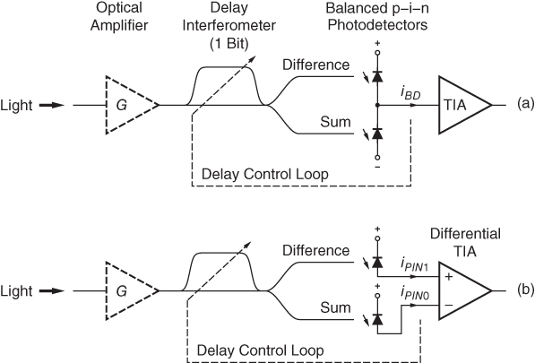
Figure 3.31 Self-coherent DPSK demodulator followed by a balanced photodetector connected to (a) a single-ended and (b) a differential TIA.
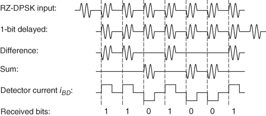
Figure 3.32 Detection of an optical RZ-DPSK signal.
In Fig. 3.31(a) the subtraction is done by means of Kirchhoff's current law [100], whereas in Fig. 3.31(b) the subtraction is done by means of a differential TIA [101–103]. The single-ended-TIA arrangement has the advantage of requiring only one connection from the detector to the TIA. The differential-TIA arrangement, however, may achieve a lower capacitance per input (only one photodetector per input) and thus a higher bandwidth [102]. Moreover, the differential-TIA arrangement requires only a single photodetector bias voltage, which can be lower than in the case of two stacked photodetectors.
The delay interferometer must be very precise. For two 1,550-nm light waves to be phase aligned within a couple of degrees at the coupler, the relative length of the two arms must be accurate to about ![]() or better. To meet this high accuracy, the delay of one arm is made tunable and a feedback mechanism controls the delay (indicated by the dashed delay control loop in Fig. 3.31) [100]. The delay can be fine tuned by either a fiber heater or a piezoelectric fiber stretcher. The error signal for the feedback control can be derived, for example, from the DC current through one of the photodiodes [100].
or better. To meet this high accuracy, the delay of one arm is made tunable and a feedback mechanism controls the delay (indicated by the dashed delay control loop in Fig. 3.31) [100]. The delay can be fine tuned by either a fiber heater or a piezoelectric fiber stretcher. The error signal for the feedback control can be derived, for example, from the DC current through one of the photodiodes [100].
Signal and Noise
Neglecting losses in the delay interferometer, we find with Eq. (3.18) that the current in each photodetector swings between approximately 0 and ![]() where
where ![]() is the responsivity of the p–i–n detectors,
is the responsivity of the p–i–n detectors, ![]() is the gain of the optical preamplifier, and
is the gain of the optical preamplifier, and ![]() is the on power of the optical input signal (
is the on power of the optical input signal (![]() for 50% RZ-DPSK).
for 50% RZ-DPSK).
The balanced detector subtracts the currents of the two photodetectors and produces the bipolar current ![]() swinging between
swinging between ![]() and
and ![]() (cf. Fig. 3.32).
(cf. Fig. 3.32).
The balanced DPSK detector generates the same amount of noise for the zeros and the ones. The amplitude distribution of the noise from a balanced detector with optical amplifier(s) is significantly non Gaussian, especially in its tails [104]. The noise currents from the individual p–i–n photodiodes, ![]() and
and ![]() , have chi-square distributions, as we know from Section 3.3. The distribution of the “dark” photodiode is strongly non-Gaussian, whereas the illuminated photodiode is closer to Gaussian. The total noise from the balanced detector,
, have chi-square distributions, as we know from Section 3.3. The distribution of the “dark” photodiode is strongly non-Gaussian, whereas the illuminated photodiode is closer to Gaussian. The total noise from the balanced detector, ![]() , is the difference of the two individual and independent noise currents,
, is the difference of the two individual and independent noise currents, ![]() . Hence the distribution of
. Hence the distribution of ![]() is the convolution of the distribution of
is the convolution of the distribution of ![]() with the distribution of
with the distribution of ![]() .
.
Detection of DQPSK
A more accurate term for DPSK would be differential binary phase-shift keying (DBPSK) because the phase difference between two successive symbols takes on one of two values (![]() or
or ![]() ). DPSK can be generalized to more than two phase values. In particular, for four values the format is known as differential quadrature phase-shift keying (DQPSK).
). DPSK can be generalized to more than two phase values. In particular, for four values the format is known as differential quadrature phase-shift keying (DQPSK).
A detector for the DQPSK format with two delay interferometers and two balanced detectors is shown in Fig. 3.33 [105, 106]. The incoming optical signal is split into two identical copies, each one feeding a seperate delay interferometer. Because each DQPSK symbol encodes two bits, the differential delay must now be set to two bit periods (one symbol period). Moreover, instead of fine tuning the interferometer arms for a ![]() phase difference, one interferometer must be tuned for
phase difference, one interferometer must be tuned for ![]() and the other must be tuned for
and the other must be tuned for ![]() .
.
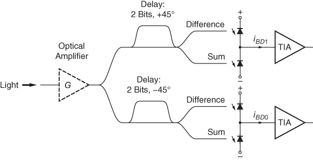
Figure 3.33 Self-coherent DQPSK demodulator followed by two balanced detectors.
How are the four phase differences of the DQPSK signal, ![]() ,
, ![]() ,
, ![]() , and
, and ![]() , detected with this arrangement? Before attempting to answer this question, let us go back to the DBPSK detector in Fig. 3.31 and look at it in a more general way. Figure 3.34(a) shows all possible phase differences between the previous and the current symbol,
, detected with this arrangement? Before attempting to answer this question, let us go back to the DBPSK detector in Fig. 3.31 and look at it in a more general way. Figure 3.34(a) shows all possible phase differences between the previous and the current symbol, ![]() , as points on a circle. The
, as points on a circle. The ![]() phase, corresponding to a zero bit, is marked by a white dot and the
phase, corresponding to a zero bit, is marked by a white dot and the ![]() phase, corresponding to a one bit, is marked by a black dot. We know that for these two points the balanced detector produces a negative and a positive current,
phase, corresponding to a one bit, is marked by a black dot. We know that for these two points the balanced detector produces a negative and a positive current, ![]() , respectively. What happens for the phases in between? For the entire right half circle, the lower photodiode receives more light than the upper one and the total output current is negative; conversely, for the entire left half circle, the upper photodiode receives more light than the lower one and the total output current is positive.
, respectively. What happens for the phases in between? For the entire right half circle, the lower photodiode receives more light than the upper one and the total output current is negative; conversely, for the entire left half circle, the upper photodiode receives more light than the lower one and the total output current is positive.
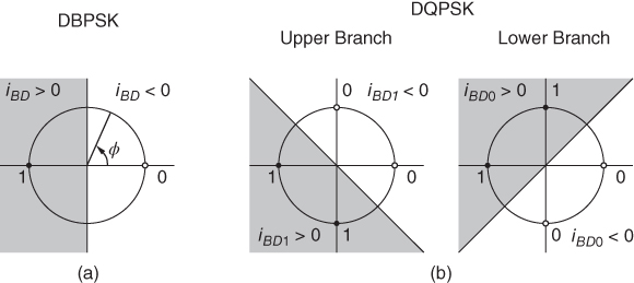
Figure 3.34 Detector currents as a function of the phase difference between successive symbols: (a) DBPSK and (b) DQPSK.
Now we are ready to analyze the DQPSK detector. Figure 3.34(b) shows the polarity of the output currents from the upper and lower balanced detectors as a function of the symbol phase difference. Because the interferometers are offset by ![]() and
and ![]() , the decision boundaries are rotated by
, the decision boundaries are rotated by ![]() counter-clockwise and
counter-clockwise and ![]() clockwise, respectively. As a result, each of the four phases is assigned a unique two-bit code. The
clockwise, respectively. As a result, each of the four phases is assigned a unique two-bit code. The ![]() and
and ![]() phases, corresponding to the DBPSK constellation, are assigned 00 and 11 and the new
phases, corresponding to the DBPSK constellation, are assigned 00 and 11 and the new ![]() and
and ![]() phases are assigned 01 and 10, respectively (note that this is a Gray code).
phases are assigned 01 and 10, respectively (note that this is a Gray code).
Detection of BPSK and QPSK
How can we demodulate and detect phase-modulated optical signals that do not encode the information differentially? Examples of such modulation formats are binary phase-shift keying (BPSK) and quadrature phase-shift keying (QPSK).
The key idea is to use a local-oscillator (LO) laser that provides a reference against which the phase of the received signal can be measured. A receiver that makes use of interference between the received signal and an LO is known as a coherent receiver (cf. Fig. 3.9). In contrast, the DBPSK and DQPSK receivers discussed earlier make use of interference between the received signal and (a delayed copy of) itself and are known as self-coherent receivers.
Some advanced modulation formats, such as dual-polarization quadrature phase-shift keying (DP-QPSK), encode information in both polarization states, requiring a detector that can recover both polarization states.
Coherent Detector with Phase and Polarization Diversity
Figure 3.35 shows the basic structure of a detector that can recover the phase and polarization information. The received optical signal and the LO wave each pass through a polarization splitter separating the ![]() -polarized component (upper path) from the
-polarized component (upper path) from the ![]() -polarized component (lower path). Then, the received signal and the LO wave pass through an array of four interferometers converting phase information to intensity information. Two of the interferometers have equal input path lengths, extracting the in-phase information, and the other two have path lengths that differ by a
-polarized component (lower path). Then, the received signal and the LO wave pass through an array of four interferometers converting phase information to intensity information. Two of the interferometers have equal input path lengths, extracting the in-phase information, and the other two have path lengths that differ by a ![]() phase shift, extracting the quadrature information. The four interferometers are followed by four balanced photodetectors providing electrical signals for the in-phase
phase shift, extracting the quadrature information. The four interferometers are followed by four balanced photodetectors providing electrical signals for the in-phase ![]() -polarized component (IX), quadrature
-polarized component (IX), quadrature ![]() -polarized component (QX), in-phase
-polarized component (QX), in-phase ![]() -polarized component (IY), and quadrature
-polarized component (IY), and quadrature ![]() -polarized component (QY).
-polarized component (QY).
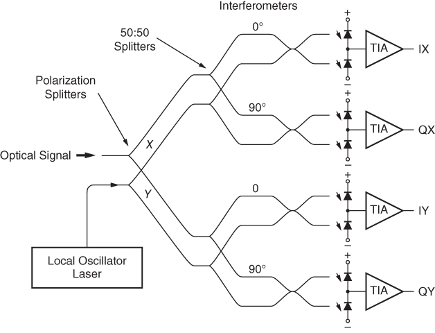
Figure 3.35 Coherent detector with phase and polarization diversity.
If the LO laser in Fig. 3.35 is phase (and frequency) locked to the transmitting laser, the coherent detector directly outputs the demodulated baseband signal. The phase locking can be achieved with an optical phase-locked loop (PLL). This approach, which is known as a homodyne receiver, however, is difficult to implement in practice [1, 107].
A better approach is to use a free-running LO laser operating at a frequency that is slightly different from the transmitter frequency (cf. Fig. 3.9). The coherent detector then outputs a phase-modulated electrical signal at a lower frequency known as the intermediate frequency (IF). The IF is given by the difference between the transmitter and LO frequency. This approach is known as a heterodyne receiver or, if the IF is so low that it falls within the signal bandwidth, as an intradyne receiver [1, 107]. The demodulation of the IF signal is done in the electrical domain, preferably with a digital signal processor (DSP) after A/D conversion (cf. Fig. 1.4) [108].
Figure 3.36 shows a packaged coherent receiver suitable for 100-![]() DP-QPSK. A PIC implementing a coherent receiver front-end including the fiber couplers, splitters, interferometers, and photodetectors is described in [56].
DP-QPSK. A PIC implementing a coherent receiver front-end including the fiber couplers, splitters, interferometers, and photodetectors is described in [56].

Figure 3.36 A packaged coherent receiver with four TIAs suitable for 100- DP-QPSK (
 ). One fiber pig tail is for the input signal, the other is for the local-oscillator laser.
Source: Reprinted by permission from Finisar Corporation.
Signal and Noise: Single Photodetector
Before analyzing the signal and noise of a coherent receiver with balanced detectors, as shown in Fig. 3.35, let us go back to the simpler situation of a coherent receiver with a single photodetector, as illustrated in Fig. 3.9.
Because of the square-law characteristic of the photodetector, we expect to get three electrical beat components from the two optical sources: ![]() . Working out the details and assuming that the polarization of the LO and the signal are aligned, we find [1]
. Working out the details and assuming that the polarization of the LO and the signal are aligned, we find [1]
where ![]() is the received power,
is the received power, ![]() is the LO power,
is the LO power, ![]() is the (angular) intermediate frequency (IF), and
is the (angular) intermediate frequency (IF), and ![]() is the phase difference between the received signal and the LO.
is the phase difference between the received signal and the LO.
The first term, ![]() , represents a DC current. For example, with an LO power of
, represents a DC current. For example, with an LO power of ![]() and
and ![]() , a constant current of
, a constant current of ![]() flows through the detector. With the usual large LO power, the third term,
flows through the detector. With the usual large LO power, the third term, ![]() , is small compared with the first term (
, is small compared with the first term (![]() ) and can be neglected. The second term is the desired IF signal that contains the phase information
) and can be neglected. The second term is the desired IF signal that contains the phase information ![]() . This term increases with
. This term increases with ![]() , which means that a larger LO power results in a stronger IF signal. In a sense, the LO provides gain, but we cannot compare this gain directly with the gain of an APD or an optical preamplifier because the LO gain acts on
, which means that a larger LO power results in a stronger IF signal. In a sense, the LO provides gain, but we cannot compare this gain directly with the gain of an APD or an optical preamplifier because the LO gain acts on ![]() whereas the APD gain and the optical-preamplifier gain act on
whereas the APD gain and the optical-preamplifier gain act on ![]() .
.
Assuming that the received optical signal is noise free (no ASE noise from optical amplifiers), the noise current after detection is mostly shot noise due to the LO laser. A secondary noise component is the relative intensity noise (RIN), also due to the LO laser. Neglecting the dark current of the detector, the mean-square noise current is [1]
where ![]() is the RIN noise of the LO. Note that this noise current does not depend on the received signal strength
is the RIN noise of the LO. Note that this noise current does not depend on the received signal strength ![]() . With the usual large LO power, the noise distribution is close to Gaussian.
. With the usual large LO power, the noise distribution is close to Gaussian.
Signal and Noise: Balanced Photodetector
Now, let us move on to the balanced detector shown in Fig. 3.37. The optical coupler produces the sum and difference of the fields from the LO and the received signal. Each output provides half of the total optical power. The currents from the two photodetectors are subtracted at the common node producing the difference ![]() .
.

Figure 3.37 Coherent receiver with balanced photodetector.
Given perfect symmetry between the two optical paths and the two detectors, the balanced output current contains only the desired second term of Eq. (3.30):
The first and third terms of Eq. (3.30) make the same current contributions to both detectors and thus cancel out. Similarly, the RIN noise current from Eq. (3.31) appears equally at both detectors and cancels out [1, 12]. The two shot-noise currents, however, are uncorrelated and do not cancel:
The balanced detector thus has the important advantages of getting rid of the RIN noise and using the signal and LO power efficiently.
The subtraction of the two photocurrents can be done by means of Kirchhoff's current law, as shown in Fig. 3.37 [109], or by means of a differential TIA (cf. Fig. 3.31(b)) [110]. The pros and cons are similar to those discussed earlier for the DPSK detector.
Common-Mode Rejection
In practice, the symmetry of a balanced detector is not perfect, which means that the RIN noise and the DC current are not completely canceled. The asymmetry is quantified by the common-mode rejection ratio (CMRR), which is determined by applying equal optical signals to both detectors and measuring the ratio [111, 112]

Typically, ![]() or less than
or less than ![]() . (Note that with the definition Eq. (3.34) a smaller value for
. (Note that with the definition Eq. (3.34) a smaller value for ![]() corresponds to a better rejection.) An imbalance in power or a mismatch in delay both result in a nonzero CMRR. A power imbalance can result from a deviation in the 50/50 splitting ratio of the coupler or unequal responsivities of the detectors. A delay mismatch can result from differences in the path length from the output of the coupler to the two photodetectors [113].
corresponds to a better rejection.) An imbalance in power or a mismatch in delay both result in a nonzero CMRR. A power imbalance can result from a deviation in the 50/50 splitting ratio of the coupler or unequal responsivities of the detectors. A delay mismatch can result from differences in the path length from the output of the coupler to the two photodetectors [113].
Advantages of Coherent Detection
The self-coherent detector for DQPSK in Fig. 3.33 and the coherent detector for DP-QPSK in Fig. 3.35 both use interference to demodulate the phase information. But there is an important difference: The self-coherent detector compares the phase of a received symbol to a noisy reference (a previously received symbol), whereas the coherent detector compares the phase of a received symbol to an essentially noise-free reference (the local oscillator). For this reason the coherent receiver requires less OSNR to operate at the desired BER.
We introduced the coherent detector with phase and polarization diversity as a means for detecting phase modulated signal. However, this is only one of its advantages over the simple intensity detector. Other important advantages are:
- The phase and polarization information that is now available in the electrical domain permits the near perfect compensation of propagation impairments, such as chromatic dispersion and polarization mode dispersion [108, 114].
- The coherent detector can be tuned to a specific wavelength by tuning the LO laser while achieving a high level of signal rejection of neighboring channels without the need for optical filters [108].
- The coherent detector features a high optical sensitivity (minimum signal power that can be detected; cf. Section 4.4), which extends the reach of unamplified transmission systems [113].
3.6 Summary
The most common photodetectors for optical receivers are:
- The p–i–n photodetector, which has a typical responsivity in the range of 0.6 to
 (at
(at  to
to  ). Vertically illuminated p–i–n detectors are suitable for speeds up to about
  and edge-coupled p–i–n detectors (waveguide and traveling-wave detectors) are suitable for speeds from 40 to more than
  . The primary noise mechanism is shot noise.
 - The avalanche photodetector (APD), which has a typical total responsivity in the range of 5 to
 (at
(at  to
to  ). Fast APDs are suitable for
  but do not provide much internal gain at
  . The primary noise mechanism is avalanche noise, quantified by the excess noise factor
  .
. - The optically preamplified p–i–n detector, which can have a total responsivity of several hundreds A/W. The optical preamplifier usually is an erbium-doped fiber amplifier (EDFA). This detector is suitable for applications from 10 to more than
 , with the p–i–n detector being the speed-limiting device. The primary noise mechanism of the optical preamplifier is amplified spontaneous emission (ASE), quantified by the noise figure
  . The p–i–n detector converts the optical ASE noise into two electrical noise components: signal–spontaneous and spontaneous–spontaneous beat noise.
 - The coherent detector, which in its basic form consists of a local-oscillator laser, a beam combiner, and a p–i–n detector. When adding phase and polarization diversity it can demodulate advanced modulation formats such as DP-QPSK. This detector is suitable for applications up to more than
 , with the p–i–n detector being the speed-limiting device. The primary noise mechanism is shot noise due to the local oscillator.
The first three detectors are characterized by:
- A photocurrent
 that is proportional to the received optical power
  . Therefore, a 3-dB change in optical power results in a 6-dB change in current.
 - A signal-dependent noise current. Specifically, the mean-square noise current
 grows proportional to the signal current
  (neglecting dark-current noise and spontaneous–spontaneous beat noise). Received one bits contain more noise than zero bits; the noise is not additive.
 - A non-Gaussian noise distribution with a steep roll-off toward zero (left side). The skew is most pronounced for small optical powers.
In contrast, the coherent detector generates a current that is proportional to the square root of the received optical power ![]() . Under typical conditions, the noise is signal independent and approximately Gaussian.
. Under typical conditions, the noise is signal independent and approximately Gaussian.
Optoelectronic integrated circuits (OEIC) combine optical devices, such as detectors, with electronic circuits, such as TIAs. Of particular interest are optical devices that are compatible with CMOS technology (silicon photonics). Examples of detectors that are suitable for integration with a circuit technology are:
- The germanium detector, which is compatible with CMOS technology.
- The metal–semiconductor–metal (MSM) detector, which can be implemented, in a standard MESFET or HFET technology.
- The spatially modulated light (SML) detector, which can be implemented in a standard CMOS technology.
To make an intensity detector sensitive to optically phase-modulated signals, the phase information must be converted to intensity information by means of optical interference. A differential phase-shift keying (DPSK) signal can be detected with a delay interferometer followed by a balanced detector. A phase-shift keying (PSK) or quadrature amplitude modulation (QAM) signal can be detected with a coherent detector with phase diversity. A signal utilizing both polarization modes (e.g., DP-QPSK) can be detected with a coherent detector with phase and polarization diversity.
Problems
-
3.1 Optical versus Electrical dBs. A p–i–n photodetector in a 1.55-
 transmission system converts the received optical signal to an electrical signal. By how many dBs is the latter signal attenuated if we splice an additional
  of standard SMF into the system?
 -
3.2 Power Conservation in the Photodiode. The p–i–n photodetector produces a current that is proportional to the received optical power
 . When this current passes through a resistor, it produces a voltage drop that is also proportional to the received optical power. Thus, the electrical power dissipated in the resistor is proportional to
  . We conclude that for large values of
  , the electrical power will exceed the received optical power! Is energy conservation violated?
 -
3.3 Sensitivity of an Antenna. An antenna is exposed to the signal power
 and thermal background radiation at the temperature
  . (a) Calculate the power level
  at which the rms signal from the antenna becomes equal to the rms value of the noise in the bandwidth
  (sensitivity at
  ). Tip: the noise from the antenna is equal to that of the resistor
  (the radiation resistance) at temperature
  [115]. (b) Evaluate the sensitivity of a receiver operating at frequency
  with noise bandwidth
  and background temperature
  . (c) Compare the sensitivity in (a) to the fundamental sensitivity limit given in [17]:3.35
-
3.4 Shot Noise Versus Thermal Noise. The current generated in a p–i–n photodetector consists of a stream of randomly arriving electrons and thus exhibits shot noise. Does the current from a battery loaded by a resistor also exhibit shot noise?
-
3.5 Amplified Shot Noise. An APD with deterministic amplification (every primary carrier generates precisely
 secondary carriers) produces the mean-square noise
  (Eq. (3.14)). Now, we could argue that the DC current produced by the APD is
  and thus the associated shot noise should be
  . What is wrong with this argument?
 -
3.6 Optically Preamplified p–i–n Detector. Extend Eq. (3.19) for
 to include the shot noise due to the signal power, shot noise due to the ASE power, and shot noise due to the detector dark current.
 -
3.7 Optical Signal-to-Noise Ratio. Equations (3.20) and (3.21) state the relationship between SNR and OSNR for a continuous-wave signal with power
 . How does this expression change for a DC-balanced ideal NRZ-modulated signal with high extinction and an average power
  ?
? -
3.8 Noise Figure of an Optical Amplifier. (a) Extend Eq. (3.26) for the noise figure
 to include the shot noise due to the signal power, shot noise due to the ASE power, and shot noise due to the detector dark current. (b) How large is the noise figure for
  , assuming
  ? (c) How large must
  be for
  , assuming
  and
and  ?
? -
3.9 Noise Figure of a Fiber. (a) Calculate the noise figure
 of an optical fiber with loss
  (
( ). (b) Calculate the noise figure
  of an optical system consisting of an optical fiber with loss
  (
( ) followed by an EDFA with gain
  and noise figure
  . (c) Calculate the noise figure
  of an optical system with
  segments, where each segment consists of an optical fiber with loss
  (
( ) followed by an EDFA with compensating gain
  and noise figure
  .
.
References
- 1 G. P. Agrawal. Fiber-Optic Communication Systems. John Wiley & Sons,Inc., Hoboken, NJ, 4th edition, 2010.
- 2 J. M. Senior. Optical Fiber Communications: Principles and Practice. Prentice Hall, Harlow, England, 3rd edition, 2009.
- 3 K. Kato. Ultrawide-band/high-frequency photodetectors. IEEE Trans. Microwave Theory Tech., MTT-47(7):1265–1281, 1999.
- 4 P. R. Berger. MSM photodiodes. IEEE Potentials, 15(2):25–29, 1996.
- 5 S. M. Sze and K. K. Ng. Physics of Semiconductor Devices. John Wiley & Sons, Inc., Hoboken, NJ, 3nd edition, 2007.
- 6 J. E. Bowers and C. A. Burrus Jr. Ultrawide-band long-wavelength p-i-n photodetectors. J. Lightwave Technol., LT-5(10):1339–1350, 1987.
- 7 M. Achouche, V. Magnin, J. Harari, D. Carpentier, E. Derouin, C. Jany, and D. Decoster. Design and fabrication of a p-i-n photodiode with high responsivity and large alignment tolerances for 40-Gb/s applications. IEEE Photonics Technol. Lett., 18(4):556–558, 2006.
- 8 S. B. Alexander. Optical Communication Receiver Design. SPIE Press, copublished with IEE, Bellingham, WA, 1997.
- 9 Y. Ota, R. G. Swartz, J. S. Schafer, M. M. Banu, A. E. Dunlop, W. C. Fischer, and T. J. Gabara. Low cost, low power digital optical receiver module for 50 Mb/s passive optical network. Int. J. High Speed Electron. Syst., 7(4):471–489, 1996.
- 10 H. Ransijn. Receiver and transmitter IC design, May 2001. CICC'2001 Ed. Session 3-2.
- 11 Y. M. Greshishchev. Front-end circuits for optical communications. In Proceedings of ISSCC'2001 Tutorial, February 2001.
- 12 M. M.-K. Liu. Principles and Applications of Optical Communications. Irwin, McGraw-Hill, Chicago, 1996.
- 13 Daghighian, H. Personal communications, 2015.
- 14 B. L. Kasper, O. Mizuhara, and Y.-K. Chen. High bit-rate receivers, transmitters, and electronics. In I. P. Kaminow and T. Li, editors, Optical Fiber Telecommunications IVA, pages 784–851. Academic Press, San Diego, CA, 2002.
- 15 K. S. Giboney, R. L. Nagarajan, T. E. Reynolds, S. T. Allen, R. P. Mirin, M. J. W. Rodwell, and J. E. Bowers. Travelling-wave photodetectors with 172-GHz bandwidth and 76-GHz bandwidth-efficiency product. IEEE Photonics Technol. Lett., 7(4):412–414, 1995.
- 16 J. D. Kraus. Antennas. McGraw Hill, New York, 2nd edition, 1988.
- 17 B. M. Oliver. Thermal and quantum noise. Proc. IEEE, 53(5):436–454, 1965.
- 18 H. Melchior, M. B. Fisher, and F. R. Arams. Photodetectors for optical communication systems. Proc. IEEE, 58(10):1466–1486, 1970.
- 19 A. E. Siegman. The antenna properties of optical heterodyne receivers. Proc. IEEE, 54(10):1350–1356, 1966.
- 20 W. V. Sorin. Noise sources in optical measurements. In D. Derickson, editor, Fiber Optic Test and Measurement, pages 597–613. Prentice Hall PTR, Upper Saddle River, NJ, 1998.
- 21 D. Johns and K. Martin. Analog Integrated Circuit Design. John Wiley & Sons, Inc., New York, 1997.
- 22 H. Ito, S. Kodama, Y. Muramoto, T. Furuta, T. Nagatsuma, and T. Ishibashi. High-speed and high-output InP-InGaAs unitraveling-carrier photodiodes. IEEE J. Sel. Top. Quantum Electron., 10(4):709–727, 2004.
- 23 S. Itakura, K. Sakai, T. Nagatsuka, E. Ishimura, M. Nakaji, H. Otsuka, K. Mori, and Y. Hirano. High-current backside-illuminated photodiode array module for optical analog links. J. Lightwave Technol., LT-28(6):965–971, 2010.
- 24 J. C. Campbell. Recent advances in telecommunications avalanche photodiodes. J. Lightwave Technol., LT-25(1):109–121, 2007.
- 25 Maxim Integrated Products. Low-noise APD bias circuit. Maxim Application Note 1831, December 2002.
- 26 J. Williams. Bias voltage and current sense circuits for avalanche photodiodes. Linear Technology Corp., Application Note 92, November 2002.
- 27 Y. Kang, H.-D. Liu, M. Morse, M. J. Paniccia, M. Zadka, S. Litski, G. Sarid, A. Pauchard, Y.-H. Kuo, H.-W. Chen, W. S. Zaoui, J. E. Bowers, A. Beling, D. C. McIntosh, X. Zheng, and J. C. Campbell. Monolithic germanium/silicon avalanche photodiodes with 340 GHz gain-bandwidth product. Nat. Photonics Lett., 3:59–63, 2009.
- 28 K. Shiba, T. Nakata, T. Takeuchi, T. Sasaki, and K. Makita. 10 Gbit/s asymmetric waveguide APD with high sensitivity of −30 dBm. Electron. Lett., 42(20):1177–1178, 2006.
- 29 G. S. Kinsey, J. C. Campbell, and A. G. Dentai. Waveguide avalanche photodiode operating at 1.55 µm with a gain-bandwidth product of 320 GHz. IEEE Photonics Technol. Lett., 13(8):842–844, 2001.
- 30 T. Nakata, T. Takeuchi, K. Makita, Y. Amamiya, T. Kato, Y. Suzuki, and T. Torikai. High-sensitivity 40-Gb/s reciever with a wideband InAlAs waveguide avalanche photodiode. In European Conference on Optical Communication (ECOC), Copenhagen, Denmark, 2002.
- 31 S. D. Personick. Receiver design for optical fiber systems. Proc. IEEE, 65(12):1670–1678, 1977.
- 32 R. J. McIntyre. The distribution of gains in uniformly multiplying avalanche photodiodes: theory. IEEE Trans. Electron Devices, ED-19(6):703–713, 1972.
- 33 R. J. McIntyre. A new look at impact ionization—part I: a theory of gain, noise, breakdown probability, and frequency response. IEEE Trans. Electron Devices, ED-46(8):1623–1631, 1999.
- 34 T. V. Muoi. Receiver design for high-speed optical-fiber systems. J. Lightwave Technol., LT-2(3):243–267, 1984.
- 35 H. J. R. Dutton. Understanding Optical Communications. Prentice Hall PTR, Upper Saddle River, NJ, 1998.
- 36 R. Ramaswami, K. N. Sivarajan, and G. Sasaki. Optical Networks: A Practical Perspective. Morgan Kaufmann Publishers, San Francisco, CA, 3rd edition, 2010.
- 37 B. Mason, J. M. Geary, J. M. Freund, A. Ougazzaden, C. Lentz, K. Glogovsky, G. Przybylek, L. Peticolas, F. Walters, L. Reynolds, J. Boardman, T. Kercher, M. Rader, D. Monroe, L. Ketelsen, S. Chandrasekhar, and L. L. Buhl. 40Gb/s photonic integrated receiver with −17 dBm sensitivity. In Optical Fiber Communication Conference (OFC), Anaheim, CA, 2002.
- 38 A. K. Srivastave and Y. Sun. Advances in erbium-doped fiber amplifiers. In I. P. Kaminow and T. Li, editors, Optical Fiber Telecommunications IVA, pages 174–212. Academic Press, San Diego, CA, 2002.
- 39 J. L. Zyskind, J. A. Nagel, and H. D. Kidorf. Erbium-doped fiber amplifiers for optical communications. In I. P. Kaminow and T. L. Koch, editors, Optical Fiber Telecommunications IIIB, pages 13–68. Academic Press, San Diego, CA, 1997.
- 40 D. A. Fishman and B. S. Jackson. Transmitter and receiver design for amplified lightwave systems. In I. P. Kaminow and T. L. Koch, editors, Optical Fiber Telecommunications IIIB, pages 69–114. Academic Press, San Diego, CA, 1997.
- 41 J. L. Rebola and A. V. T. Cartaxo. Q-factor estimation and impact of spontaneous–spontaneous beat noise on the performance of optically preamplified systems with arbitrary optical filtering. J. Lightwave Technol., LT-21(1):87–95, 2003.
- 42 R. C. Steele, G. R. Walker, and N. G. Walker. Sensitivity of optically preamplified receivers with optical filtering. IEEE Photonics Technol. Lett., 3(6):545–547, 1991.
- 43 D. M. Baney. Characterization of erbium-doped fiber amplifiers. In D. Derickson, editor, Fiber Optic Test and Measurement, pages 519–595. Prentice Hall PTR, Upper Saddle River, NJ, 1998.
- 44 E. L. Goldstein and L. Eskildsen. Erbium-doped fiber amplifiers for multiwavelength lightwave networks: Impact of the non-flat gain spectrum. In T. P. Lee, editor, Current Trends in Optical Amplifiers and Their Applications, pages 37–54. World Scientific, Singapore, 1996.
- 45 D. Marcuse. Calculation of bit-error probability for a lightwave system with optical amplifiers and post-detection Gaussian noise. J. Lightwave Technol., LT-9(4):505–513, 1991.
- 46 V. W. S. Chan. Coding and error correction in optical fiber communications systems. In I. P. Kaminow and T. L. Koch, editors, Optical Fiber Telecommunications IIIA, pages 42–62. Academic Press, San Diego, CA, 1997.
- 47 P. A. Humblet and M. Azizolu. On the bit-error rate of lightwave systems with optical amplifiers. J. Lightwave Technol., LT-9(11):1576–1582, 1991.
- 48 J. G. Proakis and M. Salehi. Digital Communications. McGraw Hill, New York, 5th edition, 2008.
- 49 W. Imajuku and A. Takada. Noise figure of phase-sensitive parametric amplifier using a Mach-Zehnder interferometer with lossy Kerr media and noisy pump. IEEE J. Quantum Electron., 39(6):799–812, 2003.
- 50 H. A. Haus. Optimum noise performance of optical amplifiers. IEEE J. Quantum Electron., 37(6):813–823, 2001.
- 51 S. Namiki, K. Seo, N. Tsukiji, and S. Shikii. Challenges of Raman amplification. Proc. IEEE, 94(5):1024–1035, 2006.
- 52 K. Rottwitt and A. J. Stentz. Raman amplification in lightwave communication systems. In I. P. Kaminow and T. Li, editors, Optical Fiber Telecommunications IVA, pages 213–257. Academic Press, San Diego, CA, 2002.
- 53 S. Namiki and Y. Emori. Ultrabroad-band Raman amplifiers pumped and gain-equalized by wavelength-division-multiplexed high-power laser diodes. IEEE J. Sel. Top. Quantum Electron., 7(1):3–16, 2001.
- 54 G. Charlet and S. Bigo. Upgrading WDM submarine systems to 40-Gbit/s channel bitrate. Proc. IEEE, 94(5):935–951, 2006.
- 55 C. Doerr, L. Chen, D. Vermeulen, T. Nielsen, S. Azemati, S. Stulz, G. McBrien, X.-M. Xu, B. Mikkelsen, M. Givehchi, C. Rasmussen, and S.-Y. Park. Single-chip silicon photonics 100-Gb/s coherent transceiver. In Optical Fiber Communication Conference (OFC), San Francisco, CA, 2014.
- 56 C. R. Doerr, P. J. Winzer, Y.-K. Chen, S. Chandrasekhar, M. S. Rasras, L. Chen, T.-Y. Liow, K.-W. Ang, and G.-Q. Lo. Monolithic polarization and phase diversity coherent receiver in silicon. J. Lightwave Technol., LT-28(4):520–525, 2010.
- 57 I. A. Young, E. Mohammed, J. T. S. Liao, A. M. Kern, S. Palermo, B. A. Block, M. R. Reshotko, and P. L. D. Chang. Optical I/O technology for tera-scale computing. IEEE J. Solid-State Circuits, SC-45(1):235–248, 2010.
- 58 B. Analui, D. Guckenberger, D. Kucharski, and A. Narasimha. A fully integrated 20-Gb/s optoelectronic transceiver implemented in a standard 0.13-µm CMOS SOI technology. IEEE J. Solid-State Circuits, SC-41(12):2945–2955, 2006.
- 59 P. C. P. Chen, A. M. Pappu, Z. Fu, W. Wattanapanitch, and A. B. Apsel. A 10 Gb/s optical receiver in 0.25 µm silicon-on-sapphire CMOS. In Proceedings of IEEE International Symposium on Circuits and Systems, pages 193–196, Seattle, WA, May 2008.
- 60 A. Emami-Neyestanak, D. Liu, G. Keeler, N. Helman, and M. Horowitz. A 1.6Gb/s, 3mW CMOS receiver for optical communication. In Symposium on VLSI Circuits Digest of Technical Papers, pages 84–87, June 2002.
- 61 K. W. Goossen, J. E. Cunningham, G. Zhang, and J. A. Walker. Very large arrays of flip-chip bonded 1.55 µm photodetectors. J. Lightwave Technol., LT-16(6):1056–1061, 1998.
- 62 A. Narasimha, B. Analui, Y. Liang, T. J. Sleboda, S. Abdalla, E. Balmater, S. Gloeckner, D. Guckenberger, M. Harrison, R. G. M. P. Koumans, D. Kucharski, A. Mekis, S. Mirsaidi, D. Song, and T. Pinguet. A fully integrated 4 × 10-Gb/s DWDM optoelectronic transceiver implemented in a standard 0.13 µm CMOS SOI technology. IEEE J. Solid-State Circuits, SC-42(12):2736–2744, 2007.
- 63 S. Palermo, A. Emami-Neyestanak, and M. Horowitz. A 90 nm CMOS 16 Gb/s transceiver for optical interconnects. IEEE J. Solid-State Circuits, SC-43(5):1235–1246, 2008.
- 64 M. Dagenais, R. F. Leheny, H. Temkin, and P. Bhattacharya. Applications and challenges of OEIC technology: a report on the 1989 Hilton Head workshop. J. Lightwave Technol., LT-8(6):846–862, 1990.
- 65 S. J. Koester, C. L. Schow, L. Schares, G. Dehlinger, J. D. Schaub, F. E. Doany, and R. A. John. Ge-on-SOI-detector/Si-CMOS-amplifier receivers for high-performance optical-communication applications. J. Lightwave Technol., LT-25(1):46–57, 2007.
- 66 K. Takahata, Y. Muramoto, H. Fukano, K. Kato, A. Kozen, S. Kimura, Y. Imai, Y. Miyamoto, O. Nakajima, and Y. Matsuoka. Ultrafast monolithic receiver OEIC composed of multimode waveguide p-i-n photodiode and HEMT distributed amplifier. IEEE J. Sel. Top. Quantum Electron., 6(1):31–37, 2000.
- 67 S. van Waasen, A. Umbach, U. Auer, H.-G. Bach, R. M. Bertenburg, G. Janssen, G. G. Mekonnen, W. Passenberg, R. Reuter, W. Schlaak, C. Schramm, G. Unterbörsch, P. Wolfram, and F.-J. Tegude. 27-GHz bandwidth high-speed monolithic integrated optoelectronic photoreceiver consisting of a waveguide fed photodiode and an InAlAs/InGaAs-HFET traveling wave amplifier. IEEE J. Solid-State Circuits, SC-32(9):1394–1401, 1997.
- 68 R. H. Walden. A review of recent progress in InP-based optoelectronic integrated circuit receiver front-ends. In K.-C. Wang, editor, High-Speed Circuits for Lightwave Communications, pages 319–330. World Scientific, Singapore, 1999.
- 69 A. Jayakumar, M. S. Bustos, D. Cheskis, S. J. Pietrucha, M. Bonelli, S. Al-Kuran, and N. Scheinberg. 3-V MSM-TIA for gigabit Ethernet. IEEE J. Solid-State Circuits, SC-35(9):1271–1275, 2000.
- 70 C. Takano, K. Tanaka, A. Okubora, and J. Kasahara. Monolithic integration of 5-Gb/s optical receiver block for short-distance communication. IEEE J. Solid-State Circuits, SC-27(10):1431–1433, 1992.
- 71 O. Wada, T. Hamaguchi, S. Miura, M. Makiuchi, K. Nakai, H. Horimatsu, and T. Sakurai. AlGaAs/GaAs p-i-n photodiode/preamplifier monolithic photoreceiver integrated on semi-insulating GaAs substrate. Appl. Phys. Lett., 46(10):981–983, 1985.
- 72 M. Ghioni, F. Zappa, V. P. Kesan, and J. Warnock. A VLSI-compatible high-speed silicon photodetector for optical data link applications. IEEE Trans. Electron Devices, ED-43(7):1054–1060, 1996.
- 73 G. N. Nasserbakht, J. W. Adkisson, B. A. Wooley, J. S. Harris Jr., and T. I. Kamins. A monolithic GaAs-on-Si receiver front end for optical interconnect systems. IEEE J. Solid-State Circuits, SC-28(6):622–630, 1993.
- 74 J. Sturm, M. Leifhelm, H. Schatzmayr, S. Groiß, and H. Zimmermann. Optical receiver IC for CD/DVD/blue-laser application. IEEE J. Solid-State Circuits, SC-40(7):1406–1413, 2005.
- 75 R. Swoboda, J. Knorr, and H. Zimmermann. A 5-Gb/s OEIC with voltage-up-converter. IEEE J. Solid-State Circuits, SC-40(7):1521–1526, 2005.
- 76 R. Swoboda and H. Zimmermann. 11Gb/s monolithically integrated silicon optical receiver for 850nm wavelength. In ISSCC Digest of Technical Papers, pages 240–241, February 2006.
- 77 D. Kucharski, D. Guckenberger, G. Masini, S. Abdalla, J. Witzens, and S. Sahni. 10Gb/s 15mW optical receiver with integrated germanium photodetector and hybrid inductor peaking in 0.13 µm SOI CMOS technology. In ISSCC Digest of Technical Papers, pages 360–361, February 2010.
- 78 T.-Y. Liow, K.-W. Ang, Q. Fang, J.-F. Song, Y.-Z. Xiong, M.-B. Yu, G.-Q. Lo, and D.-L. Kwong. Silicon modulators and germanium photodetectors on SOI: monolithic integration, compatibility, and performance optimization. IEEE J. Sel. Top. Quantum Electron., 16(1):307–315, 2010.
- 79 J. Choi, B. J. Sheu, and O. T.-C. Chen. A monolithic GaAs receiver for optical interconnect systems. IEEE J. Solid-State Circuits, SC-29(3):328–331, 1994.
- 80 K. D. Pedrotti, R. L. Pierson Jr., N. H. Sheng, R. B. Nubling, C. W. Farley, and M. F. Chang. High-bandwidth OEIC receivers unsing heterojunction bipolar transistors: design and demonstration. J. Lightwave Technol., LT-11(10):1601–1614, 1992.
- 81 S. Radovanović, A.-J. Annema, and B. Nauta. A 3-Gb/s optical detector in standard CMOS for 850-nm optical communication. IEEE J. Solid-State Circuits, SC-40(8):1706–1717, 2005.
- 82 D. L. Rogers. Integrated optical receivers using MSM detectors. J. Lightwave Technol., LT-9(12):1635–1638, 1991.
- 83 J. B. D. Soole and H. Schumacher. Transit-time limited frequency response of InGaAs MSM photodetectors. IEEE Trans. Electron Devices, ED-37(11):2285–2291, 1990.
- 84 B. J. van Zeghbroeck, W. Patrick, J.-M. Halbout, and P. Vettiger. 105-GHz bandwidth metal-semiconductor-metal photodiode. IEEE Electron Device Lett., EDL-9(10):527–529, 1988.
- 85 C. Rooman, D. Coppée, and M. Kuijk. Asynchronous 250-Mb/s optical receivers with integrated detector in standard CMOS technology for optocoupler applications. IEEE J. Solid-State Circuits, SC-35(7):953–958, 2000.
- 86 W.-Z. Chen, S.-H. Huang, G.-W. Wu, C.-C. Liu, Y.-T. Huang, C.-F. Chiu, W.-H. Chang, and Y.-Z. Juang. A 3.125 Gbps CMOS fully integrated optical receiver with adaptive analog equalizer. In Proceedings of IEEE Asian Solid-State Circuits Conference (ASSCC), pages 396–399, November 2007.
- 87 Y. Dong and K. W. Martin. A high-speed fully-integrated POF receiver with large-area photo detectors in 65 nm CMOS. IEEE J. Solid-State Circuits, SC-47(9):2080–2092, 2012.
- 88 T. S.-C. Kao, F. A. Musa, and A. C. Carusone. A 5-Gbit/s CMOS optical receiver with integrated spatially modulated light detector and equalization. IEEE Trans. Circuits Syst. I, CASI-57(11):2844–2857, 2010.
- 89 F. Tavernier and M. S. J. Steyaert. High-speed optical receivers with integrated photodiode in 130 nm CMOS. IEEE J. Solid-State Circuits, SC-44(10):2856–2867, 2009.
- 90 A. C. Carusone, H. Yasotharan, and T. Kao. CMOS technology scaling considerations for multi-Gbps optical receivers with integrated photodetectors. IEEE J. Solid-State Circuits, SC-46(8):1832–1842, 2011.
- 91 J. Genoe, D. Coppée, J. H. Stiens, R. A. Vounckx, and M. Kuijk. Calculation of the current response of the spatially modulated light CMOS detector. IEEE Trans. Electron Devices, ED-48(9):1892–1902, 2001.
- 92 C. Hermans and M. S. J. Steyaert. A high-speed 850-nm optical receiver front-end in 0.18-µm CMOS. IEEE J. Solid-State Circuits, SC-41(7):1606–1614, 2006.
- 93 T. K. Woodward and A. V. Krishnamoorthy. 1 Gb/s CMOS photoreceiver with integrated detector operating at 850 nm. Electron. Lett., 34(12):1252–1253, 1998.
- 94 W.-Z. Chen and S.-H. Huang. A 2.5 Gbps CMOS fully integrated optical receiver with lateral pin detector. In Proceedings of IEEE Custom Integrated Circuits Conference, pages 293–296, September 2007.
- 95 S.-H. Huang and W.-Z. Chen. A 10-Gbps CMOS single chip optical receiver with 2-d meshed spatially-modulated light detector. In Proceedings of IEEE Custom Integrated Circuits Conference, pages 129–132, September 2009.
- 96 S.-H. Huang, W.-Z. Chen, Y.-W. Chang, and Y.-T. Huang. A 10-Gb/s OEIC with meshed spatially-modulated photo detector in 0.18-µm CMOS technology. IEEE J. Solid-State Circuits, SC-46(5):1158–1169, 2011.
- 97 D. Lee, J. Han, G. Han, and S. M. Park. An 8.5-Gb/s fully integrated CMOS optoelectronic receiver using slope-detection adaptive equalizer. IEEE J. Solid-State Circuits, SC-45(12):2861–2873, 2010.
- 98 A. H. Gnauck and P. J. Winzer. Optical phase-shift-keyed transmission. J. Lightwave Technol., LT-23(1):115–130, 2005.
- 99 P. J. Winzer and R.-J. Essiambre. Advanced optical modulation formats. Proc. IEEE, 94(5):952–984, 2006.
- 100 E. A. Swanson, J. C. Livas, and R. S. Bondurant. High sensitivity optically preamplified direct detection DPSK receiver with active delay-line stabilization. IEEE Photonics Technol. Lett., 6(2):263–265, 1994.
- 101 H. Fukuyama, T. Itoh, T. Furuta, K. Kurishima, M. Tokumitsu, and K. Murata. Two-channel InP HBT differential automatic-gain-controlled transimpedance amplifier IC for 43-Gbit/s DQPSK photoreceiver. In Compound Semiconductor Integrated Circuit Symposium (CSICS), pages 1–4, Monterey, CA, October 2008.
- 102 J. H. Sinsky, A. Adamiecki, A. Gnauck, C. A. Burrus Jr., J. Leuthold, O. Wohlgemuth, S. Chandrasekhar, and A. Umbach. RZ-DPSK transmission using a 42.7-Gb/s integrated balanced optical front end with record sensitivity. J. Lightwave Technol., LT-22(1):180–185, 2004.
- 103 J. S. Weiner, A. Leven, V. Houtsma, Y. Baeyens, Y.-K. Chen, P. Paschke, Y. Yang, J. Frackoviak, W.-J. Sung, A. Tate, R. Reyes, R. F. Kopf, and N. G. Weimann. SiGe differential transimpedance amplifier with 50-GHz bandwidth. IEEE J. Solid-State Circuits, SC-38(9):1512–1517, 2003.
- 104 H. Kim and P. J. Winzer. Nonlinear phase noise in phase-coded transmission. In Optical Fiber Communication Conference (OFC), Anaheim, CA, 2005.
- 105 C. R. Doerr, D. M. Gill, A. H. Gnauck, L. L. Buhl, P. J. Winzer, M. A. Cappuzzo, A. Wong-Foy, E. Y. Chen, and L. T. Gomez. Monolithic demodulator for 40-Gb/s DQPSK using a star coupler. J. Lightwave Technol., LT-24(1):171–174, 2006.
- 106 R. A. Griffin and A. C. Carter. Optical Differential Quadrature Phase-Shift Key (oDQPSK) for High Capacity Optical Transmission. Optical Fiber Communication Conference (OFC), Anaheim, CA, 2002.
- 107 A. Leven, N. Kaneda, U.-V. Koc, and Y. K. Chen. Feed-forward phase and frequency estimation in coherent digital and analog photonic links using digital signal processing. In Microwave Symposium, Honolulu, HI, June 2007.
- 108 K. Roberts, S. H. Foo, M. Moyer, M. Hubbard, A. Sinclair, J. Gaudette, and C. Laperle. High capacity transport—100G and beyond. J. Lightwave Technol., LT-33(3):563–578, 2015.
- 109 J. Zhang, J. Verbist, B. Moeneclaey, J. van Weerdenburg, R. van Uden, H. Chen, J. van Campenhout, C. Okonkwo, X. Yin, J. Bauwelinck, and G. Roelkens. Compact low-power-consumption 28-Gbaud QPSK/16-QAM integrated silicon photonics/electronic coherent receiver. IEEE Photonics J., 8(1):1–10, 2016.
- 110 A. Awny, R. Nagulapalli, D. Micusik, J. Hoffmann, G. Fischer, D. Kissinger, and A. C. Ulusoy. A dual 64Gbaud 10kΩ 5% THD linear differential transimpedance amplifier with automatic gain control in 0.13 µm BiCMOS technology for optical fiber coherent receivers. In ISSCC Digest of Technical Papers, pages 406–407, February 2016.
- 111 OIF. Implementation Agreement for Integrated Dual Polarization Micro-Intradyne Coherent Receivers – IA # OIF-DPC-MRX-01.0. Optical Internetworking Forum, Fremont, CA, March 2015.
- 112 Y. Painchaud, M. Poulin, M. Morin, and M. Têtu. Performance of balanced detection in a coherent receiver. OSA Opt. Express, 17(5):3659–3672, 2009.
- 113 B. Zhang, C. Malouin, and T. J. Schmidt. Design of coherent receiver optical front end for unamplified applications. OSA Opt. Express, 20(3):3225–3234, 2012.
- 114 S. J. Savory, G. Gavioli, R. I. Killey, and P. Bayvel. Electronic compensation of chromatic dispersion using a digital coherent receiver. OSA Opt. Express, 15(5):2120–2126, 2007.
- 115 L. W. Couch II. Digital and Analog Communication Systems. Prentice Hall, Upper Saddle River, NJ, 7th edition, 2006.