
5
THE PER-UNIT-LENGTH PARAMETERS FOR MULTICONDUCTOR LINES
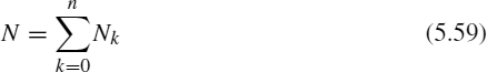
In this chapter, we will extend the notions developed for two-conductor lines in the previous chapter to multiconductor lines. In general, the concepts are identical but the details are more involved. We will find that numerical approximate methods must generally be employed to compute the entries in the per-unit-length parameter matrices L, C, and G. The entries in the per-unit-length resistance matrix R are grouped as shown in Chapter 3, Eqs. (3.12) and (3.13), and are computed, as an approximation, for the isolated conductors. Hence, the entries in R are the same as were obtained for two-conductor lines in the previous chapter; that is, we disregard proximity effect in the resistance calculation.
In the case of multiconductor transmission lines (MTLs), the situation is somewhat similar except that the details become more involved. In the case of a MTL where the conductors have circular, cylindrical cross sections such as wires and the surrounding medium is homogeneous, we can obtain approximate closed-form solutions for the entries in the per-unit-length parameter matrices L, C, and G under the assumption that the conductors are widely separated from each other. This condition of being widely separated is not very restrictive for typical dimensions of wire-type lines such as ribbon cables. However, dielectric insulations are usually present around the conductors of wire-type lines such as ribbon cables, and therefore wire-type MTLs generally require the use of numerical methods to compute the entries in the per-unit-length parameter matrices. For the case of MTLs having conductors of rectangular cross sections such as lands on printed circuit boards (PCBs), approximate numerical methods must always be used regardless of whether the surrounding medium is homogeneous (as is the case for the coupled stripline) or inhomogeneous (as for the case of the coupled microstrip and the case of a general PCB).
5.1 DEFINITIONS OF THE PER-UNIT-LENGTH PARAMETER MATRICES L, C, AND G
We first review the fundamental definitions of the per-unit-length parameter matrices of inductance, L, capacitance, C, and conductance, G. Recall that these per-unit-length parameters are determined as static field solutions in the transverse plane for perfect line conductors. As opposed to two-conductor lines, there are only a few closed-form solutions for MTLs. Generally, approximate numerical methods must be used for the computation of the entries in the per-unit-length parameter matrics L, C, and G. In any event, we showed in Chapter 3 that L, C, and G are symmetric and positive-definite matrices. Again, we will restrict our discussions to uniform lines. As discussed previously, computation of the entries in R is identical to those calculations for two-conductor lines given previously; that is, we will neglect proximity effect and compute these entries for isolated conductors.
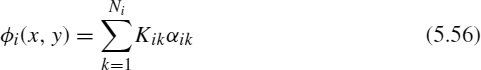
The entries in the per-unit-length inductance matrix L relate the total magnetic flux penetrating the ith circuit, per unit of line length, to all the line currents producing it as
or, in expanded form,
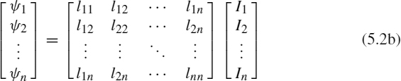
If we interpret the above relations in a manner similar to the n-port parameters [A.2], we obtain the following relations for the entries in L:
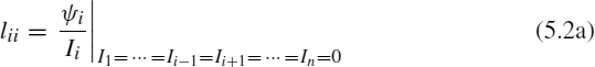
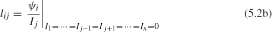
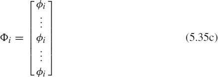
The entries lii are the self-inductances of the ith circuit, and the entries lij with i ≠ j are the mutual inductances between the ith and the jth circuits. Thus, we can compute these inductances by placing a current on one conductor (and returning it on the reference conductor), setting the currents on all other conductors to zero, and determining the magnetic flux, per unit of line length, penetrating the other circuit. The definition of the ith circuit is critically important in obtaining the correct value and sign of these elements. This important concept is illustrated in Figure 5.1. The ith circuit is the surface between the ith conductor and the reference conductor. This surface is of arbitrary shape but is uniform along the line. This surface shape may be a flat surface or some other shape so long as this shape is uniform along the line. The magnetic flux per unit length penetrating this surface (circuit) is defined as being in the clockwise direction around the ith conductor when looking in the direction of increasing z. In other words, the flux direction ψi through surface si is the direction in which magnetic flux would be generated by the current of the ith conductor. Figure 5.1(a) shows the calculation of lii, and Figure 5.1(b) shows the calculation of lij.
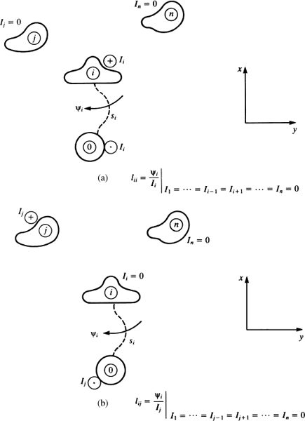
FIGURE 5.1 Illustration of the definitions of flux through a circuit for determination of the per-unit-length inductances: (a) self-inductances lii and (b) mutual inductances lij.
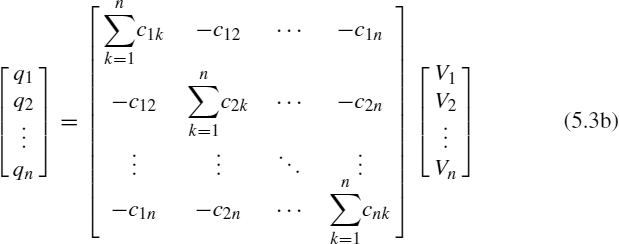
In order to illustrate this important concept further, consider a three-conductor line consisting of three wires lying in a plane where the middle wire is chosen, arbitrarily, as the reference conductor as shown in Figure 5.2(a). This resembles a ribbon cable without dielectric insulations. The surfaces and individual configurations for computing l11, l22, and l12 are shown in the remaining figures. Observe that the surface for ψ2 is between conductor 2 and the reference conductor, but observe the desired direction of this flux; it is chosen with respect to the magnetic flux that would be produced by current I2 on conductor 2. So, the flux direction for the ith circuit is defined by the direction of the current on the ith conductor and the right-hand rule when looking in the direction of increasing z.
The entries in the per-unit-length capacitance matrix C relate the total charge on the ith conductor per unit of line length to all of the line voltages producing it as or, in expanded form,
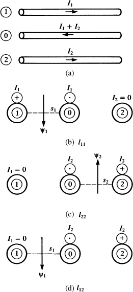
FIGURE 5.2 Illustrations of the derivation of the per-unit-length inductances for a three-wire ribbon cable with the center wire as the reference conductor.
The particular form for the entries in C in (5.3b) was derived in Chapter 3. If we denote the entries in C in the ith row and jth column as [C]ij, these can be obtained by interpreting (5.3b) as an n-port relation and applying the usual constraints of setting all voltages except the jth voltage Vj to zero (“grounding” them to the reference conductor) and determining the charge qi on the ith conductor (and −qi on the reference conductor) to give [C]ij:
This amounts to several two-conductor capacitance calculations where the other n − 1 conductors are connected with short circuits to the reference conductor.
Although the above method of setting all but one voltage to zero and determining the resulting per-unit-length charge on the other conductors is straightforward, an alternative and simpler method is to apply a per-unit-length charge qj on the jth conductor, the negative of this, −qj, on the reference conductor, and zero charge on the other conductors and then determining the resulting voltage between the ith conductor and the reference conductor. In order to do this, we invert (5.3) to give
or, in expanded form,
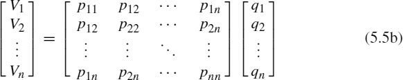
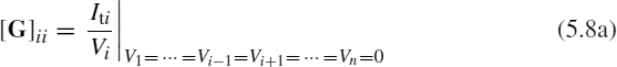
The entries in P are referred to as the coefficients of potential. Once the entries in P are obtained, C is obtained via (5.5c). The coefficients of potential are obtained from (5.5b) as
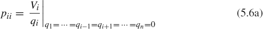
These relationships show that to determine pij we place a per-unit-length charge qj on conductor j with no charge on the other conductors (but −qj on the reference conductor) and determine the resulting voltage Vi of conductor i (between it and the reference conductor with the voltage positive at the ith conductor). These concepts are illustrated in Figure 5.3. Once P is obtained in this fashion, C is obtained as the inverse of P as shown in (5.5c). It is important to point out that the self-capacitance between the ith conductor and the reference conductor, cii, is not simply the entry in the ith row and ith column of C. Observe the form of the entries in C given in (5.3b). The off-diagonal entries are the negatives of the mutual capacitances between the pairs of conductors whereas the main-diagonal entries are the sum of the selfcapacitance and the mutual capacitances in that row (or column). Therefore, to obtain the self-capacitance cii, we sum the entries in the ith row (or column) of C.
The per-unit-length conductance matrix G relates the total transverse conduction current passing between the conductors per unit of line length to all the line voltages producing it as
or, in expanded form,
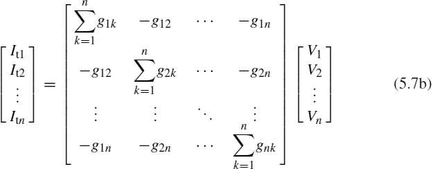
The particular forms of the entries in G in (5.7b) were obtained in Chapter 3.
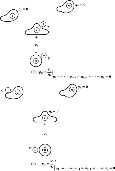
FIGURE 5.3 Illustrations of the determination of the per-unit-length coefficients of potential: (a) self terms pii and (b) mutual terms pij.
Once again, the entries in G can be determined as several subproblems by interpreting (5.7b) as an n-port. For example, to determine the entry in G in the ith row and jth column, which is denoted as [G]ij, we could enforce a voltage between the jth conductor and the reference conductor, Vj, with all other conductor voltages set to zero (“grounding” them to the reference conductor), V1 = ··· Vj−1 = Vj+1 = ··· Vn = 0, and determine the per-unit-length transverse current Iti flowing between the ith conductor and the reference conductor. Denoting each of the entries in G as [G]ij gives these entries in G as
In order to numerically determine the entries in L, C, and G, we need only a capacitance solver. First, we solve for the scalar capacitance matrix with the dielectric(s) surrounding the conductors removed and replaced with free space that is denoted as C0. The per-unit-length inductance matrix can be obtained from
In order to obtain the per-unit-length capacitance and conductance matrices, we could, as an alternative to the direct method outlined before, use the capacitance solver with each dielectric replaced by its complex permittivity:
where tan δi is the loss tangent (at the particular frequency of interest) of the ith dielectric layer and tan δi = (σeff, i/εi). This will give a complex-valued capacitance matrix as
Then, as discussed in the previous chapter, we obtain the per-unit-length capacitance and conductance matrices as
and
and ω = 2πf is the radian frequency of interest.
5.1.1 The Generalized Capacitance Matrix 
The above definitions as well as the derivation of the MTL equations assume that we (arbitrarily) select one of the n + 1 conductors as the reference conductor to which all the n voltages Vi are referenced. Once the reference conductor is chosen, all the per-unit-length parameter matrices must be computed for that choice consistently. Although the choice of reference conductor is arbitrary, choosing one of the n + 1 conductors over another as reference may facilitate the computation of the per-unit-length parameters. For example, if one of the n + 1 conductors is an infinite, perfectly conducting plane, choosing the plane as the reference conductor simplifies the calculation of the per-unit-length parameters. However, choice of this plane as reference is not mandatory; we could instead choose one of the other n conductors as the reference conductor. In this section, we describe a technique for computing a certain per-unit-length parameter matrix, the generalized capacitance matrix ![]() without regard to the choice of the reference conductor. The dimensions of this generalized capacitance matrix are (n + 1) × (n + 1). We will show that a transmission-line capacitance C which is of dimensions n × n, for any conductor chosen as reference conductor can be easily obtained from this generalized capacitance matrix. If a different choice of the reference conductor is made, we can readily obtain the transmission-line capacitance matrix C for this new choice of reference conductor from the generalized capacitance matrix using simple algebraic relations without repeating the time-consuming calculation of the per-unit-length generalized capacitance. The generalized capacitance matrix for the line with the surrounding medium removed and replaced by free space,
without regard to the choice of the reference conductor. The dimensions of this generalized capacitance matrix are (n + 1) × (n + 1). We will show that a transmission-line capacitance C which is of dimensions n × n, for any conductor chosen as reference conductor can be easily obtained from this generalized capacitance matrix. If a different choice of the reference conductor is made, we can readily obtain the transmission-line capacitance matrix C for this new choice of reference conductor from the generalized capacitance matrix using simple algebraic relations without repeating the time-consuming calculation of the per-unit-length generalized capacitance. The generalized capacitance matrix for the line with the surrounding medium removed and replaced by free space, ![]() , and the generalized capacitance matrix with the permittivities replaced by their complex-valued permittivities given in (5.10) as
, and the generalized capacitance matrix with the permittivities replaced by their complex-valued permittivities given in (5.10) as ![]() can similarly be obtained. The transmission-line capacitance matrix C0 and the complex transmission-line capacitance matrix
can similarly be obtained. The transmission-line capacitance matrix C0 and the complex transmission-line capacitance matrix ![]() can then be easily obtained from these corresponding generalized capacitance matrices. Then other transmission-line per-unit-length matrices L, C, and G can then be easily obtained from these as
can then be easily obtained from these corresponding generalized capacitance matrices. Then other transmission-line per-unit-length matrices L, C, and G can then be easily obtained from these as
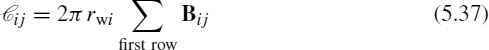
and
and
Hence, the major computational effort is in determining the generalized capacitance matrices.
The n MTL voltages Vi are defined to be between each conductor and the chosen reference conductor. We may also define the potentials ![]() i of each of the n + 1 conductors with respect to some reference point or line that is parallel to the z axis [C.4]. The total charge per unit of line length, qi, of each of the n + 1 conductors can be related to their potentials
i of each of the n + 1 conductors with respect to some reference point or line that is parallel to the z axis [C.4]. The total charge per unit of line length, qi, of each of the n + 1 conductors can be related to their potentials ![]() i for i = 0, 1, 2, …, n with the (n + 1) × (n + 1) generalized capacitance matrix
i for i = 0, 1, 2, …, n with the (n + 1) × (n + 1) generalized capacitance matrix ![]() as
as
Observe that ![]() is (n + 1) × (n + 1), whereas the previous per-unit-length parameter matrices L, C, and G are n × n. Also the generalized capacitance matrix, like the transmission-line capacitance matrix, is symmetric, that is,
is (n + 1) × (n + 1), whereas the previous per-unit-length parameter matrices L, C, and G are n × n. Also the generalized capacitance matrix, like the transmission-line capacitance matrix, is symmetric, that is, ![]() , for similar reasons. It can be shown that for a charge-neutral system, as is the case for the MTL, the reference potential terms for the choice of reference point for these potentials,
, for similar reasons. It can be shown that for a charge-neutral system, as is the case for the MTL, the reference potential terms for the choice of reference point for these potentials, ![]() i, vanish as the reference point recedes to infinity so that the choice of reference point does not affect the determination of the generalized capacitance matrix [B.4,C.1,C.4,C.7].
i, vanish as the reference point recedes to infinity so that the choice of reference point does not affect the determination of the generalized capacitance matrix [B.4,C.1,C.4,C.7].
Suppose that ![]() has been computed and we select a reference conductor. Without loss of generality, let us select the reference conductor as the zeroth conductor. In order to obtain the n × n capacitance matrix C from
has been computed and we select a reference conductor. Without loss of generality, let us select the reference conductor as the zeroth conductor. In order to obtain the n × n capacitance matrix C from ![]() , define the MTL line voltages, with respect to this zeroth reference conductor, as
, define the MTL line voltages, with respect to this zeroth reference conductor, as
for i = 1, 2, …, n. We assume that the entire system of n + 1 conductors is charge neutral:
Therefore, the charge (per unit of line length) on the zeroth conductor can be written in terms of the charges on the other n conductors as
Denote the entries in the ith row and jth column of the per-unit-length capacitance matrix C, with the zeroth conductor chosen as reference conductor, as Cij:
Comparing (5.18) to (5.3b), we observe that ![]() and Cij = −cij. Substituting (5.16) and (5.17) into (5.15) and expanding gives
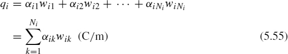
and Cij = −cij. Substituting (5.16) and (5.17) into (5.15) and expanding gives ![]() i = Vi +
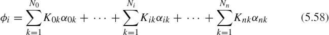
i = Vi + ![]() 0)
0)
Adding all equations in (5.19) gives
or
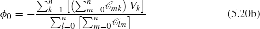
Substituting (5.20b) into the last n equations in (5.19) yields the entries in the per-unit-length capacitance matrix C, given in (5.18) as [C.4]
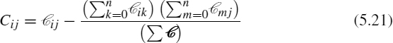
The first summation in the numerator of (5.21) is the sum of all the elements in the ith row of ![]() , whereas the second summation in the numerator of (5.21) is the sum of all the elements in the jth column of
, whereas the second summation in the numerator of (5.21) is the sum of all the elements in the jth column of ![]() . The denominator summation
. The denominator summation ![]() is the sum of all the elements in
is the sum of all the elements in ![]() .
.
In the case of two conductors, the result in (5.21) gives per-unit-length capacitance between the two conductors and reduces to
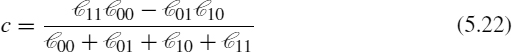
The generalized capacitance matrix, like the transmission-line capacitance, is symmetric so that ![]() . Eliminating the potential reference node (or line) and observing that capacitors in series (parallel) combine like resistors in parallel (series), one can directly obtain the result in (5.22) from the equivalent circuit of Figure 5.4(a).
. Eliminating the potential reference node (or line) and observing that capacitors in series (parallel) combine like resistors in parallel (series), one can directly obtain the result in (5.22) from the equivalent circuit of Figure 5.4(a).
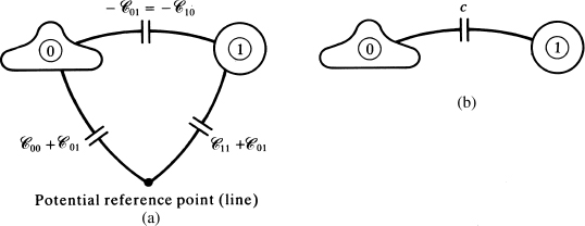
FIGURE 5.4 Illustration of (a) the meaning of the per-unit-length generalized capacitance matrix for a two-conductor line and (b) the elimination of the reference line to yield the capacitance between the conductors.
Therefore, we can obtain the per-unit-length generalized capacitance matrix ![]() , then choose a reference conductor, and then easily compute C for that choice of reference conductor from
, then choose a reference conductor, and then easily compute C for that choice of reference conductor from ![]() using the relation in (5.21). If the surrounding medium is inhomogeneous in ε, we similarly compute the generalized capacitance matrix with the dielectric removed (replaced with free space),
using the relation in (5.21). If the surrounding medium is inhomogeneous in ε, we similarly compute the generalized capacitance matrix with the dielectric removed (replaced with free space), ![]() , and from that compute the per-unit-length capacitance matrix with the dielectric removed, C0, with the above method. Once C0 is computed in this fashion, we may then compute
, and from that compute the per-unit-length capacitance matrix with the dielectric removed, C0, with the above method. Once C0 is computed in this fashion, we may then compute ![]() . Computing the complex generalized capacitance matrix using a complex permittivity for each homogeneous region as in (5.10),
. Computing the complex generalized capacitance matrix using a complex permittivity for each homogeneous region as in (5.10), ![]() , we can obtain the complex transmission-line matrix as
, we can obtain the complex transmission-line matrix as ![]() and from that we can obtain the transmission-line capacitance matrix as C = CR and the conductance matrix as G = −ωCI as shown in (5.12).
and from that we can obtain the transmission-line capacitance matrix as C = CR and the conductance matrix as G = −ωCI as shown in (5.12).
5.2 MULTICONDUCTOR LINES HAVING CONDUCTORS OF CIRCULAR, CYLINDRICAL CROSS SECTION (WIRES)
Conductors having cross sections that are circular–cylindrical are referred to as wires. These types of conductors are frequently found in cables that interconnect electronic circuitry and form an important class of MTLs.
5.2.1 Wide-Separation Approximations for Wires in Homogeneous Media
The results for two-conductor lines in a homogeneous medium obtained in the previous chapter are exact. For similar lines consisting of more than two conductors, exact, closed-form solutions cannot be obtained, in general. However, if the wires are relatively widely spaced, we can obtain some simple but approximate closed-form solutions using the fundamental subproblems derived in Section 4.2.1 of the previous chapter [B.4]. These results assume that the currents and charges are symmetric about the wire axes, which implicitly assumes that the wires are widely spaced. In other words we assume that proximity effect is not pronounced. As we saw in the case of two-wire lines, the requirement of widely spaced wires is not overly restrictive. The following wide-separation approximations for wires are implemented in the FORTRAN program WIDESEP.FOR described in Appendix A.
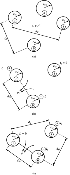
FIGURE 5.5 Illustration of the calculation of per-unit-length inductances using the wide-separation approximations for n + 1 wires: (a) the cross-sectional structure, (b) self-inductance, and (c) mutual inductance.
5.2.1.1 n+1 Wires
Consider the case of n + 1 wires in a homogeneous medium as shown in Figure 5.5(a). The entries in the per-unit-length inductance matrix are defined in (5.1) and (5.2). If the wires are widely separated, we can use the fundamental subproblems derived in Section 4.2.1 of the previous chapter to give these entries. The self-inductance is obtained from Figure 5.5(b) and the mutual inductance is obtained as in Figure 5.5(c) as
The entries in the per-unit-length capacitance and conductance matrices for this assumed homogeneous surrounding medium can be obtained from this result as before:
5.2.1.2 n Wires Above an Infinite, Perfectly Conducting Plane
Consider the case of n wires above and parallel to an infinite, perfectly conducting plane shown in Figure 5.6. Replacing the plane with the image currents and using the fundamental result derived in Section 4.2.1 of the previous chapter yields
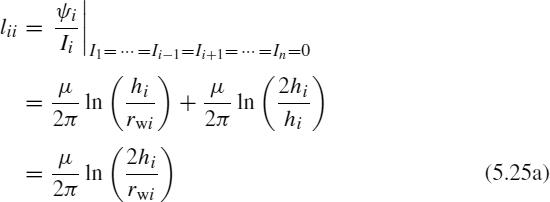
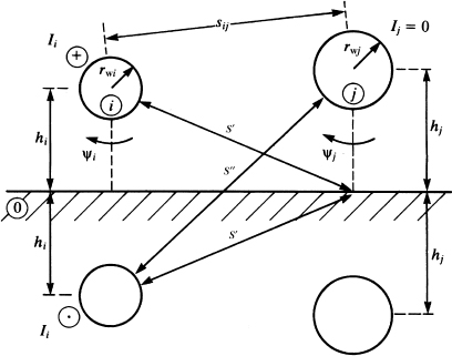
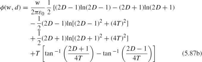
FIGURE 5.6 Illustration of the calculation of per-unit-length inductances using the wide-separation approximations for n wires above a ground plane.
This is again a problem of a homogeneous medium, and therefore the entries in the per-unit-length capacitance and conductance matrices can then be found from these results using (5.24).
5.2.1.3 n Wires Within a Perfectly Conducting Cylindrical Shield
Consider n wires of radii rwi within a perfectly conducting circular–cylindrical shield shown in Figure 5.7(a). The interior radius of the shield is denoted by rS and the distances of the wires from the shield axis are denoted by di, whereas the angular separations are denoted by θij. The perfectly conducting shield may be replaced by image currents located at radial distances from the shield center of ![]() as shown in Figure 5.7(b) [B.1, 1, 2]. The directions of the desired magnetic fluxes are as shown. Assuming that the wires are widely separated from each other and the shield, we may assume that the currents are uniformly distributed around the wire and shield peripheries. Thus, we may use the basic results of Section 4.2.1 of the previous chapter to give [B.1]
as shown in Figure 5.7(b) [B.1, 1, 2]. The directions of the desired magnetic fluxes are as shown. Assuming that the wires are widely separated from each other and the shield, we may assume that the currents are uniformly distributed around the wire and shield peripheries. Thus, we may use the basic results of Section 4.2.1 of the previous chapter to give [B.1]
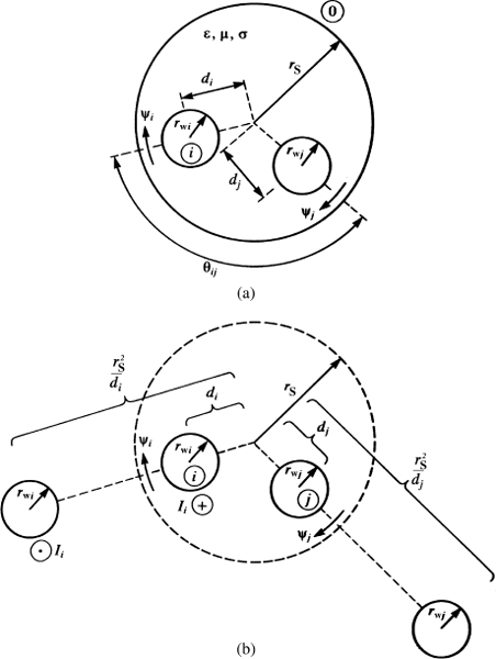
FIGURE 5.7 Illustration of the calculation of per-unit-length inductances using the wide-separation approximations for n wires within a cylindrical shield: (a) the cross-sectional structure and (b) replacement with images.
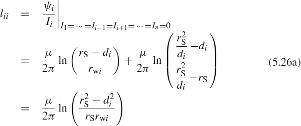
The entries in the per-unit-length capacitance and conductance matrices for this homogeneous medium can be obtained using the relations in (5.24).
5.2.2 Numerical Methods for the General Case
The results in the previous three subsections give simple formulas for the entries in the per-unit-length parameter matrices of L, C, and G for n wires and a reference conductor for three cases: (1) n + 1 wires, (2) n wires above an infinite, perfectly conducting “ground” plane, and (3) n wires within an overall circular–cylindrical shield. There are two important restrictions on their applicability. These are that (1) the wires must be widely separated and (2) the dielectric medium surrounding the wires must be homogeneous; that is, circular dielectric insulations are ignored. The wide-separation assumption provides the simplification that the charge distributions around the wire peripheries are approximately uniform. This assumption was made so that we may use the fundamental subproblems for wires derived in Section 4.2.1 of the previous chapter to obtain those results. The charge distributions around closely spaced wires will be nonuniform around their peripheries but will be approximately uniform for ratios of wire separation to wire radius of 4 and higher (see Fig. 4.9). However, a significant restriction on the utility of those results is that they assume a homogeneous surrounding dielectric medium. Practical wire-type cables have circular–cylindrical insulating dielectrics surrounding them, which creates an inhomogeneous medium (air and the dielectric insulation). In this section, we will obtain a numerical technique that can be used to obtain accurate results for multiwire lines having an inhomogeneous surrounding medium as well as closely spaced conductors. The following method is described in [C.1–C.7] and is implemented for the practical case of a ribbon cable in a FORTRAN computer program RIBBON.FOR described in Appendix A.
First, consider an (n + 1)-wire line in a homogeneous medium. If the wires are closely spaced, proximity effect will cause the charge distributions to be nonuniform around the wire peripheries. In the case of wires that are closely spaced, the charge distributions will tend to concentrate on the adjacent surfaces (proximity effect) (see Fig. 4.9). In order to model this effect, we will assume a form of the charge distribution around the ith wire periphery in the form of a Fourier series as a function of the peripheral angle θi as
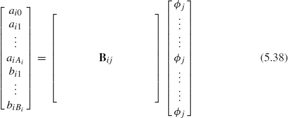
This Fourier series representation for the ith wire contains a total number of unknowns of Ni = 1 + Ai + Bi. For a line consisting of n + 1 wires, there will be a total of ![]() unknowns to be determined. The coefficients of each expansion, ai0, aik, and bik, are to be determined such that the boundary conditions are satisfied. These boundary conditions are that the potential at points on each conductor due to all charge distributions equals the potential of that conductor. (Since we assume perfect conductors for the computation of L, C, and G, the potentials of all points on a conductor are the same.) The charge distribution in (5.27) has dimensions of C/m2 since it gives the distribution around the wire periphery per unit of line length. Once the expansion coefficients in (5.27) are determined to satisfy the boundary conditions, the total charge on the ith conductor per unit of line length is obtained by integrating (5.27) around the wire periphery to yield
unknowns to be determined. The coefficients of each expansion, ai0, aik, and bik, are to be determined such that the boundary conditions are satisfied. These boundary conditions are that the potential at points on each conductor due to all charge distributions equals the potential of that conductor. (Since we assume perfect conductors for the computation of L, C, and G, the potentials of all points on a conductor are the same.) The charge distribution in (5.27) has dimensions of C/m2 since it gives the distribution around the wire periphery per unit of line length. Once the expansion coefficients in (5.27) are determined to satisfy the boundary conditions, the total charge on the ith conductor per unit of line length is obtained by integrating (5.27) around the wire periphery to yield
Hence, the charge per unit of line length is determined solely by the constant term in the expansion. However, the other terms affect this constant term. This simple result is due to the fact that ![]() .
.
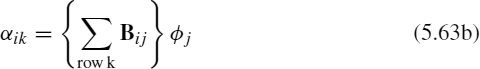
We now determine the potential at an arbitrary point in the transverse plane at a position rp, θp from each of these charge distributions, that is, ![]() i (rp, θp), as illustrated in Figure 5.8. This can be obtained by assuming that the charge distribution around the periphery of the ith conductor is composed of filaments of per-unit-length charge ρirwidθi C/m, each of whose amplitudes are weighted by the particular distribution, that is, 1, cos (kθi), and sin (kθi). Then we use the previous fundamental subproblem result given in Eq. (4.16) for the voltage between two points. With reference to Figure (5.8), we obtain
i (rp, θp), as illustrated in Figure 5.8. This can be obtained by assuming that the charge distribution around the periphery of the ith conductor is composed of filaments of per-unit-length charge ρirwidθi C/m, each of whose amplitudes are weighted by the particular distribution, that is, 1, cos (kθi), and sin (kθi). Then we use the previous fundamental subproblem result given in Eq. (4.16) for the voltage between two points. With reference to Figure (5.8), we obtain

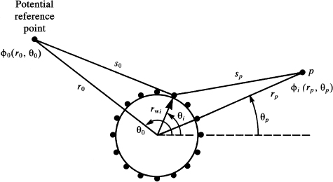
FIGURE 5.8 Determination of the potential of a charge-carrying wire having various circumferential distributions by replacement of the charge with weighted filaments of charge.
It was shown in [C.7] that the potential of the reference point, ![]() 0(r0, θ0), can be omitted if the system of conductors is electrically neutral, that is, the net charge per unit of line length is zero. Since this is satisfied for our MTL systems, we will henceforth omit the reference potential term. Thus, the differential contribution to the potential due to a filamentary component of the charge distribution is
0(r0, θ0), can be omitted if the system of conductors is electrically neutral, that is, the net charge per unit of line length is zero. Since this is satisfied for our MTL systems, we will henceforth omit the reference potential term. Thus, the differential contribution to the potential due to a filamentary component of the charge distribution is
The distance from the filament to the point is (according to the law of cosines) given by
Substituting this along with the form for the charge distribution given in (5.27) into (5.30) and integrating around the conductor periphery gives the total contribution to the potential due to the charge distributions:
where
Each of the integrals in (5.32a) can be evaluated in closed form giving [B.4]
Therefore, the contributions to the potential from each of these charge distributions are given in Table 5.1.
Satisfaction of the boundary conditions is obtained if we choose a total of
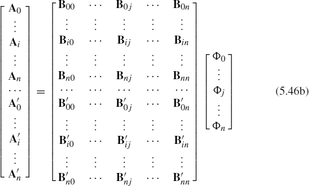
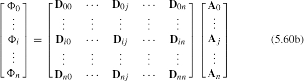
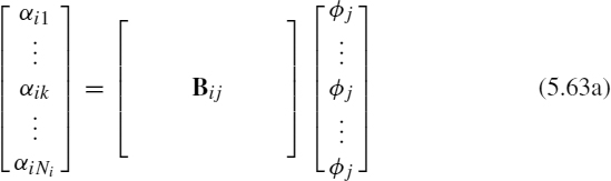
points on the wires at which we enforce the potential of the wire due to all the charge distributions on this conductor and all of the other conductors as illustrated in Figure 5.9. This leads to a set of N simultaneous equations that must be solved for the expansion coefficients, written in matrix form, as
FIGURE 5.9 Determination of the total potential at a point due to all charge distributions.
The vector of potentials at the match points on the ith conductor is denoted as
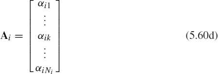
and the vector of expansion coefficients of the charge distribution on the ith conductor is denoted as
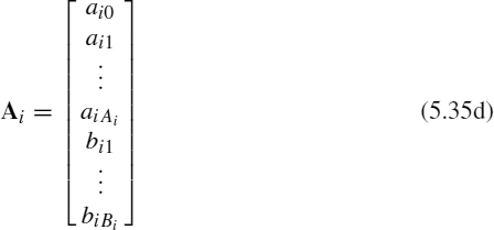
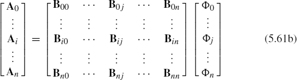
and Ai denotes the expansion coefficients associated with the ith conductor according to (5.27). Each Ai will have Ni = 1 + Ai + Bi rows as will Φi. Each Dij will have dimension of Ni × Nj. Inverting (5.35) gives the expansion coefficients in terms of a linear combination of the potentials of each conductor:
or, in expanded form,
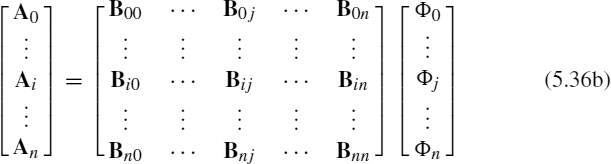
The generalized capacitance matrix ![]() described in Section 5.1.1 can be obtained from (5.36), using (5.28), as [C.1–C.7]
described in Section 5.1.1 can be obtained from (5.36), using (5.28), as [C.1–C.7]
This simple result is due to the fact that according to (5.28) we need only to determine ai0, and each submatrix in (5.36) relates
or, in expanded form,
where [Bij]mn denotes the entry in row m and column n of Bij. Hence, ![]() involves the sum of the entries in the first row of Bij.
involves the sum of the entries in the first row of Bij.
5.2.2.1 Applications to Inhomogeneous Dielectric Media
This method can be extended to handle inhomogeneous media such as circular–cylindrical dielectric insulations around the wires. Observe that for each wire and dielectric insulation of that wire there are two surfaces that contain charge and each distribution must be expanded into a Fourier series with respect to the angle around that boundary θi. These two surfaces are the conductor–dielectric surface and the dielectric–free-space surface.
As previously discussed in Chapter 4, dielectric media consist of microscopic dipoles of bound charge as illustrated in Figure 5.10(a). Application of an external electric field causes these microscopic dipoles of bound charge to align with the field as illustrated in Figure 5.10(b). If a slab of dielectric is immersed in an electric field, a bound charge density will appear on the surfaces of the dielectric as illustrated in Figure 5.10(c).
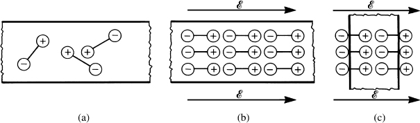
FIGURE 5.10 Illustration of the effects of bound (polarization) charge: (a) microscopic dipoles, (b) alignment of the dipoles with an applied electric field, and (c) creation of a bound surface charge.
Charge consists of two types: free charge is the charge that is free to move and bound charge is the charge appearing on the surfaces of dielectrics in response to an applied electric field as shown in Figure 5.10(c). At the interface between two dielectric surfaces, the boundary condition is that the components of the electric flux density vector ![]() that are normal to the interface must be continuous, that is,
that are normal to the interface must be continuous, that is, ![]() . A simple way of handling inhomogeneous dielectric media is to replace the dielectrics with free space having bound charge at the interface [C.1–C.7,1,2]. At places where the dielectric is adjacent to a perfect conductor, we have both free charge and bound charge, and the free charge density on the surface of the conductor is equal to the component of the electric flux density vector that is normal to the conductor surface, Dn (C/m2) [A.1]. Of course, the component of the electric field intensity vector that is tangent to a boundary is continuous across the boundary for an interface between two dielectrics,
. A simple way of handling inhomogeneous dielectric media is to replace the dielectrics with free space having bound charge at the interface [C.1–C.7,1,2]. At places where the dielectric is adjacent to a perfect conductor, we have both free charge and bound charge, and the free charge density on the surface of the conductor is equal to the component of the electric flux density vector that is normal to the conductor surface, Dn (C/m2) [A.1]. Of course, the component of the electric field intensity vector that is tangent to a boundary is continuous across the boundary for an interface between two dielectrics, ![]() , and is zero at the surface of a perfect conductor.
, and is zero at the surface of a perfect conductor.
In order to adapt the above numerical method to wires that have circular, cylindrical dielectric insulations, we describe the charge (bound plus free) around the wire periphery as a Fourier series in the peripheral angle, θi, as in (5.27):

In (5.40), ρif denotes the free charge distribution on the ith conductor periphery and ρib denotes the bound charge distribution on the dielectric periphery facing the conductor as shown in Figure 5.11. At the dielectric periphery facing the free-space region, there is only bound charge that we similarly expand in a Fourier series in peripheral angle θi as
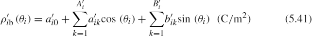
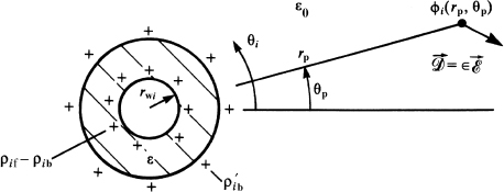
FIGURE 5.11 The general problem of the determination of the potential of a dielectric-insulated wire due to free and bound charge distributions at the two interfaces.
In (5.40), we have anticipated that the bound charge distribution at the conductor periphery will be opposite in sign to the bound charge distribution around the dielectric–free-space boundary. Also, we denote the bound charge distribution at the dielectric–free-space boundary in (5.41) with a prime, whereas the bound charge distribution at the conductor–dielectric boundary in (5.40) is denoted without a prime. This is because, although the total bound charge per unit length at each boundary must be the same, the distributions around the peripheries are different since the boundary radii are different. For each dielectric-insulated wire, there are a total of Ni unknown expansion coefficients, Ni = 1 + Ai + Bi, for the free plus bound charge on the conductor peripheries and a total of ![]() unknown expansion coefficients,
unknown expansion coefficients, ![]() , for the bound charge on the outer dielectric periphery. For a total of n + 1 wires, this gives a total number of unknowns of N + N′, where
, for the bound charge on the outer dielectric periphery. For a total of n + 1 wires, this gives a total number of unknowns of N + N′, where

unknowns. Observe that the total bound charge at the dielectric–conductor boundary per unit of line length must equal the total bound charge per unit of line length at the dielectric–free-space boundary but their distributions will not be the same. To determine the total charge on each surface per unit of line length, we integrate the charge distribution in (5.40) and (5.41) to yield
and
where ti is the thickness of the dielectric for the ith wire.
In order to enforce the boundary conditions, we choose points on each conductor periphery at which to enforce the conductor potential ![]() i and points on each dielectric–free-space periphery at which to enforce the continuity of the normal components of the electric flux density vector due to all these charge distributions. This gives a set of N + N′ simultaneous equations of a form similar to (5.35):
i and points on each dielectric–free-space periphery at which to enforce the continuity of the normal components of the electric flux density vector due to all these charge distributions. This gives a set of N + N′ simultaneous equations of a form similar to (5.35):
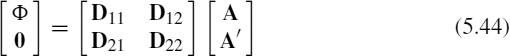
The first ![]() rows enforce the conductor potentials, and the second
rows enforce the conductor potentials, and the second ![]()
![]() rows enforce the continuity of the normal components of the electric flux density vector across the dielectric–free-space interfaces. The vector A contains the
rows enforce the continuity of the normal components of the electric flux density vector across the dielectric–free-space interfaces. The vector A contains the ![]() expansion coefficients of the free plus bound charge at the conductor peripheries, and the vector A′ contains the
expansion coefficients of the free plus bound charge at the conductor peripheries, and the vector A′ contains the ![]() expansion coefficients of the bound charge at the dielectric–free-space peripheries. The match points around the two peripheries are not chosen to be evenly spaced but are chosen with a scheme that avoids giving a singular matrix in (5.44) [C.3].
expansion coefficients of the bound charge at the dielectric–free-space peripheries. The match points around the two peripheries are not chosen to be evenly spaced but are chosen with a scheme that avoids giving a singular matrix in (5.44) [C.3].
The entries in (5.44) can be obtained by considering a cylindrical boundary of radius rb of infinite length shown in Figure 5.12, which supports the charge distributions 1, cos (mθb), and sin (mθb) around its periphery. This is identical to the problem of free charge around a conductor periphery considered in the previous section, but here the charge distribution can represent free or bound charge distributions. Proceeding as in the previous section by modeling the charge distributions as weighted filaments of charge gives the potential both inside and outside the boundary. Similarly, the electric field due to these charge distributions can be obtained from the gradient of these potential solutions [A.1]:
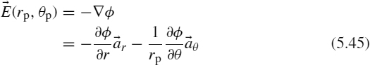
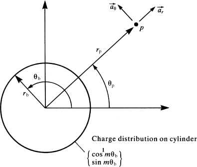
FIGURE 5.12 The general problem of determining the potential inside and outside a charge distribution.
TABLE 5.2 Match point outside the charge distribution, rp ≥ rb.
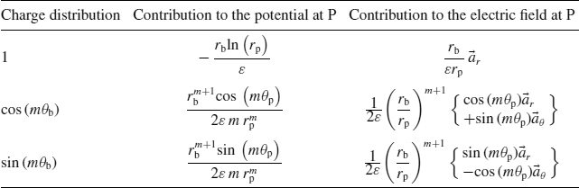
Carrying out these operations, the potential and electric field at a point rb, θb both inside and outside the charge distribution are given in Tables (5.2) and (5.3) [C.1–C.3].
Inverting Eq. (5.44) gives
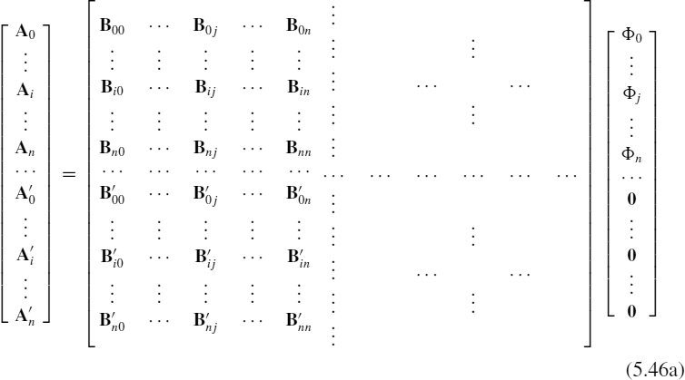
TABLE 5.3 Match point inside the charge distribution, rp < rb.
Recall that the charge at the conductor–dielectric interface consists of free charge plus bound charge, ρif−ρib. The entries in the generalized capacitance matrix relate the free charge on the conductors to the conductor potentials. Therefore, according to (5.43a) and (5.43b), we must add the total (bound) charge at the dielectric–free-space surface to the total (bound plus free) charge at the conductor–dielectric surface in order to obtain the free charge on the conductor to give the total per-unit-length free charge for each wire as
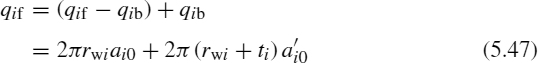
Thus, in a fashion similar to the bare conductor case above, the entries in the generalized capacitance matrix can be obtained from (5.47) as
where Σfirst rowBij denotes the sum of the elements in the first row of the submatrix Bij of (5.46b) relating the coefficients of the bound plus free charge at the ith conductor interface to the potential of the jth conductor, ![]() j, and
j, and ![]() denotes the sum of the elements in the first row of the submatrix
denotes the sum of the elements in the first row of the submatrix ![]() of (5.46b) relating the coefficients of the bound charge at the dielectric–free-space interface for the ith conductor to the potential of the jth conductor,
of (5.46b) relating the coefficients of the bound charge at the dielectric–free-space interface for the ith conductor to the potential of the jth conductor, ![]() j.
j.
FIGURE 5.13 Dimensions of a three-wire ribbon cable for illustration of numerical results.
5.2.3 Computed Results: Ribbon Cables
As an illustration of the numerical results, consider the three-wire ribbon cable shown in Figure 5.13. The outside wire is chosen for the reference conductor. The center-to-center separations of the wires are 50 mils (1 mil = 0.001 inch). The wires are identical and are composed of # 28 gauge (7 × 36) stranded wires with radii of rw = 7.5 mils and polyvinyl chloride (PVC) insulations of thickness t =10 mils and relative dielectric constant εr = 3.5. The results are computed using the RIBBON.FOR computer program described in Appendix A, which implements the method described in this section for ribbon cables. The generalized capacitance matrix was computed using 10 Fourier coefficients around each wire surface (the constant term and nine cosine terms) and 10 Fourier coefficients around each dielectric–free-space surface and the results are shown in Table 5.4.
The per-unit-length transmission-line capacitance matrices C and C0 become as shown in Table 5.5. The last column of Table 5.5 shows the effective dielectric constant (relative permittivity) as ![]() . The per-unit-length inductances shown in Table 5.6 were computed exactly as
. The per-unit-length inductances shown in Table 5.6 were computed exactly as ![]() , and using the wide-separation approximations.
, and using the wide-separation approximations.
TABLE 5.4 The generalized capacitances for the three-wire ribbon cable with and without the dielectric insulations.
TABLE 5.5 The transmission-line capacitances for the three-wire ribbon cable with and without the insulation dielectrics.
TABLE 5.6 The transmission-line inductances for the three-wire ribbon cable computed exactly and using the wide-separation approximations.
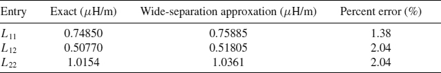
The wide-separation approximations are computed from (5.23) using the FORTRAN program WIDESEP.FOR described in Appendix A as
Once again, the wide-separation approximations give results for the entries in the per-unit-length inductance matrix that are within some 2% of the values computed from ![]() . The ratio of adjacent wire separation to wire radius is 6.67, so we would expect this.
. The ratio of adjacent wire separation to wire radius is 6.67, so we would expect this.
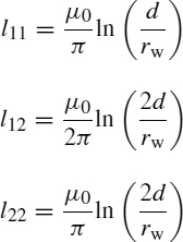
Figure 5.14 illustrates the convergence of the method for the three-wire ribbon cable. The per-unit-length inductances and per-unit-length capacitances are plotted versus the number of Fourier coefficients around the wire and dielectric boundaries in Figure 5.14(a) and (b), respectively. Observe that the inductances converge to accurate values after about two Fourier coefficients per boundary, whereas the capacitances require on the order of three or four Fourier coefficients per boundary for convergence.
FIGURE 5.14 Convergence of the per-unit-length parameters of the three-wire ribbon cable versus number of expansion coefficients: (a) inductances and (b) capacitances.
5.3 MULTICONDUCTOR LINES HAVING CONDUCTORS OF RECTANGULAR CROSS SECTION
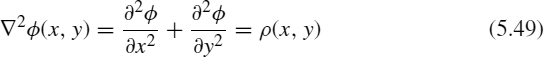
The basic solution problem in determining the entries in the per-unit-length parameter matrices L, C, and G remains the same as before. The per-unit-length parameters of inductance, capacitance, and conductance are all obtained as the static (dc) solution of the fields in the transverse x–y plane for perfect conductors. Essentially, this means that we need to solve Laplace's or Poisson's equation in the two-dimensional transverse plane [A.1]:
There are various methods for solving this equation. The method we will use determines an approximate solution using various numerical techniques that we will discuss in this section.
5.3.1 Method of Moments (MoM) Techniques
MoM techniques essentially solve integral equations where the unknown is in the integrand. An example is the integral form of Poisson's equation in the transverse x–y plane:
where a charge distribution in the x–y plane, ρ, is distributed over some surface s. Ordinarily, we know or prescribe the potential at points in the region (e.g., on perfectly conducting bodies) and wish to determine the charge distribution that produces it. Thus, we need to solve an integral equation for the integrand [A.1, 2–5].
The problems of interest here are the perfect conductors in the two-dimensional plane that are infinite in length (in the z direction) and the ith conductor that has some unknown surface charge density, ρi (x, y)(C/m2), residing on its surface as illustrated in Figure 5.15. Observe that the units of this charge distribution are per square meter: One dimension is along the z axis and the other dimension is around the conductor surface in the transverse x–y plane. One common way of doing this, which we used for the ribbon cable, is to approximate the charge distribution around the two-dimensional conductor periphery as infinitely long filaments of charge in the z direction (C/m) and use the basic problem of the potential of an infinitesimal line charge that was developed in Section 4.2.1. This forms the basis for numerical techniques that are used to analyze these two-dimensional structures of infinite length for determining the per-unit-length parameters [2–5]. Thus, we initially solve the problem of the potential of an infinitely long filament of charge carrying a per-unit-length charge in the z direction, which is uniformly distributed in the z direction. The potential at a point is the sum of the potentials of each line charge that makes up the desired charge distribution around the conductor periphery.
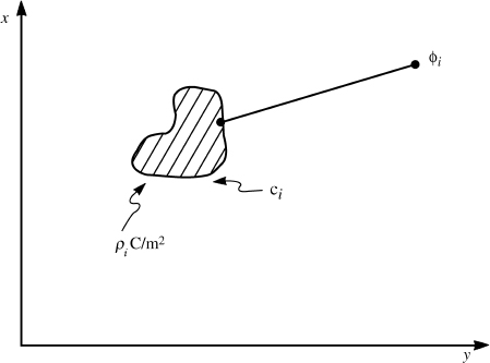
FIGURE 5.15 Illustration of the solution of Poisson's equation in two dimensions.
A more general way is to represent the charge distribution over the ith conductor surface as a linear combination of basis functions, ρik, as
Entire domain expansions use basis functions that are nonzero over the entire contour of the surface in the same manner as a Fourier series represents a time-domain function using basis functions defined over the time interval encompassing one complete period. This was the technique used earlier to expand the charge distributions around the wire and dielectric insulation peripheries of ribbon cables. Subdomain expansions seek to represent the charge distribution over discrete segments of the surface contour [C.1,C.2]. Each of the expansion basis functions, ρik, are defined over the discrete segments of the contour, cik, and are zero over the other segments. We will concentrate on the subdomain expansion method. There are many ways of choosing the expansion functions over the segments. One of the simplest ways is to represent the charge distribution as a “staircase function,” where the charge distribution is constant over the segments of the contour:
This is illustrated in Figure 5.16 and is referred to as the pulse expansion method. The charge distribution is assumed to be constant over the segments cik of the surface, but the levels αik are unknown as yet. Hence, we are making a “staircase” approximation to the true distribution. This is the essence of the MoM method that we will use for PCBs. More elaborate approximations such as triangular distributions may be made with corresponding increase in difficulty of analysis.
In order to illustrate the method as applied to PCB structures, consider a PCB shown in Figure 5.17(a) where three infinitesimally thin lands (flat, perfect conductors) reside on the surface of a dielectric substrate having a relative permittivity of εr. Each land is at potential ![]() i and carries a per-unit-length charge distribution qi (C/m). This charge distribution qi is the total charge on the land per unit of line length in the z direction. Figure 5.17(b) shows an important distinction between the case of PCB lands and the case of round wires; the charge distributions across the land widths on PCB lands, ρi(C/m2), tend to peak at the edges of the lands [6]. In order to determine the per-unit-length capacitance matrix for this structure we must relate these per-unit-length charge distributions qi to the conductor potentials
i and carries a per-unit-length charge distribution qi (C/m). This charge distribution qi is the total charge on the land per unit of line length in the z direction. Figure 5.17(b) shows an important distinction between the case of PCB lands and the case of round wires; the charge distributions across the land widths on PCB lands, ρi(C/m2), tend to peak at the edges of the lands [6]. In order to determine the per-unit-length capacitance matrix for this structure we must relate these per-unit-length charge distributions qi to the conductor potentials ![]() i, with the generalized capacitance matrix
i, with the generalized capacitance matrix ![]() as
as
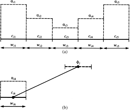
FIGURE 5.16 Illustration of the pulse expansion of a charge distribution on a flat strip.

FIGURE 5.17 Illustration of the charge distributions over the lands of a PCB.
We represent this charge distribution over each land as in (5.51) with the staircase approximation or pulse expansion method given in (5.52) as illustrated in Figure 5.18(a). The αik unknown levels of the charge distributions are to be determined to satisfy the boundary condition that the potential over the ith conductor is ![]() i as illustrated in Figure 5.18(b). The total charge (per unit length in the z direction) in C/m is obtained by summing the charges of the subsections of that conductor:
i as illustrated in Figure 5.18(b). The total charge (per unit length in the z direction) in C/m is obtained by summing the charges of the subsections of that conductor:
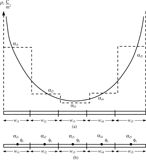
FIGURE 5.18 Illustration of (a) approximating the charge distribution over a land with piecewise-constant expansion functions and (b) matching the potential at the center of each strip.
In the case of the pulse expansion method, this simplifies to
where wik is the width of the kth segment of the ith conductor. The potential at a point on the ith conductor due to this representation will be due to the contributions from all the unknown charge distributions and can therefore be written as a linear combination of them as
Each coefficient Kik is determined as the contribution to the potential due to each basis function alone:
There are many ways of generating the required equations. One rather simple technique is the method of point matching. For illustration consider a system of n +1 conductors each having a prescribed potential of ![]() i for i = 0, 1, …,n. We next enforce the potential of each conductor,
i for i = 0, 1, …,n. We next enforce the potential of each conductor, ![]() i, due to all charge distributions in the system to be the potential of that conductor at the center of each subsection of the conductor. Typical resulting equations are of the form
i, due to all charge distributions in the system to be the potential of that conductor at the center of each subsection of the conductor. Typical resulting equations are of the form
Choosing a total of
points on the conductors gives the following set of N simultaneous equations in terms of the expansion coefficients:
The vector of potentials at the match points on the ith conductor is denoted as

and the vector of expansion coefficients of the charge distribution on the ith conductor is denoted as
Inverting (5.60) gives
or, in expanded form,
Once the expansion coefficients are obtained from (5.61), the total charge (per unit of length in the z direction in C/m) can be obtained from (5.55). The generalized capacitance matrix ![]() can then be obtained. In the case of point matching and pulse expansion functions as with flat conductors, the entries in the generalized capacitance matrix can be directly obtained from (5.61) as
can then be obtained. In the case of point matching and pulse expansion functions as with flat conductors, the entries in the generalized capacitance matrix can be directly obtained from (5.61) as

where wik is the width of the kth subsection of the ith conductor. This simple result is obtained from (5.55):
and is due to the fact that a submatrix of (5.61b) relates
Expanding this gives the expansion coefficients as
If the widths of all conductor segments are chosen to be the same and designated as w, then the elements of the generalized capacitance matrix are simplified as
where ΣBij is the sum of all the elements in the submatrix Bij.
Thus, the basic subproblem is determining Kik in (5.57), that is, determining the potential at the center of a segment due to a constant charge distribution of unit value, αik = 1(C/m2), over some other segment where that segment can be associated with another conductor. In order to illustrate this, consider the infinitesimally thin conducting strip of width w and infinite length supporting a charge distribution ρ(C/m2) that is constant along the strip cross section as shown in Figure 5.19. If we treat this as an array of wire filaments each of which bears a charge per unit of filament length of ρdx C/m, then we may determine the potential at a point as the sum of the potentials of these filaments again using the basic result for the potential of a filament given in (4.16) or (5.30) [2, 5]:
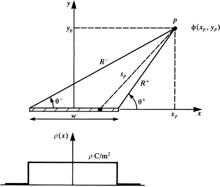
FIGURE 5.19 Calculation of the potential due to a constant charge distribution on a flat strip.
This integral is evaluated using [7]. This may be simplified somewhat if we denote the distances from the edges of the strip as R+ and R− and the angles as θ+ and θ−, as shown in Figure 5.19. In terms of these (5.65) becomes

In the case where the field or observation point lies at the midpoint of the strip in question, this becomes
The electric field due to this charge distribution will be needed for problems that involve dielectric interfaces. The electric field can be computed from this result as [A.1]
As an illustration of this method, consider the rectangular conducting box shown in Figure 5.20. The four walls are insulated from one another and are maintained at potentials of ![]() 1 = 0,
1 = 0, ![]() 2 = 10 V,
2 = 10 V, ![]() 3 = 20 V, and
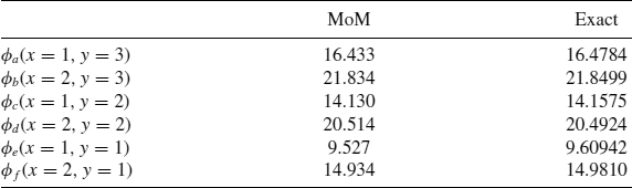
3 = 20 V, and ![]() 4 = 30 V. Suppose we divide the two vertical conductors into four segments each and the horizontal members into three segments each. Using pulse expansion functions for each segment and point matching gives 14 equations in 14 unknowns (the levels of the assumed constant charge distributions over each segment). Using the above results gives the potentials at the six interior points as shown in Table 5.7.
4 = 30 V. Suppose we divide the two vertical conductors into four segments each and the horizontal members into three segments each. Using pulse expansion functions for each segment and point matching gives 14 equations in 14 unknowns (the levels of the assumed constant charge distributions over each segment). Using the above results gives the potentials at the six interior points as shown in Table 5.7.
The exact results were obtained via a direct solution of Laplace's equation using separation of variables. In terms of the general parameters denoted in Figure 5.20, the solution is [8]
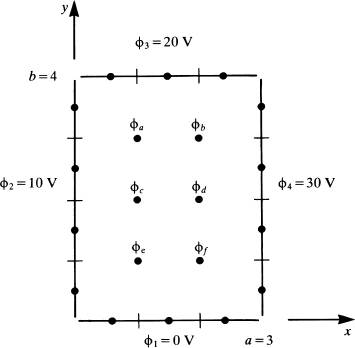
FIGURE 5.20 A two-dimensional problem for demonstration of the solution of Laplace's equation via the pulse expansion–point matching method.
TABLE 5.7
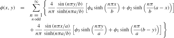
where a = 3, b = 4, and ![]() 1 = 0,
1 = 0, ![]() 2 = 10 V,
2 = 10 V, ![]() 3 = 20 V, and
3 = 20 V, and ![]() 4 = 30 V. The solution using finite-difference and finite-element methods will be given in subsequent subsections.
4 = 30 V. The solution using finite-difference and finite-element methods will be given in subsequent subsections.
The pulse expansion–point matching technique described above is particularly simple to implement in a digital computer program. Achieving convergence generally requires a rather large computational expense since the conductor subsections must be chosen sufficiently small to give an accurate representation of the charge distributions. This is particularly true in the case of lands on PCBs where the charge distribution peaks at the edges of each land. There are other choices of expansion functions such as triangles or piecewise sinusoidal functions, but the programming complexity also increases. For this reason, we will use the pulse expansion–point matching method for PCBs.
5.3.1.1 Applications to Printed Circuit Boards
The above MoM method can be adapted to the computation of the per-unit-length capacitances of conductors with rectangular cross sections as occur on PCBs. Consider a typical PCB shown in Figure 5.21(a) having infinitesimally thin conducting lands on the surface of a dielectric board of thickness t and relative dielectric constant of εr. The widths of the lands are denoted as wi and the edge-to-edge separations are denoted as sij. A direct approach would be to subsection each land into Ni segments of length wik. The charge on each subsection could be represented using the pulse expansion method as being constant over that segment with unknown level of αik. We could similarly subsection the surface of the dielectric and represent the bound charge on that surface with pulse expansions. A more direct way would be to imbed the dielectric in the basic Green's function. We will choose to do this. Thus, the problem becomes one of subsectioning the conductors immersed in free space as illustrated in Figure 5.21(b).
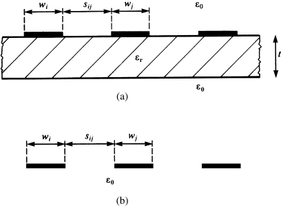
FIGURE 5.21 A PCB for illustration of the determination of the per-unit-length capacitances.
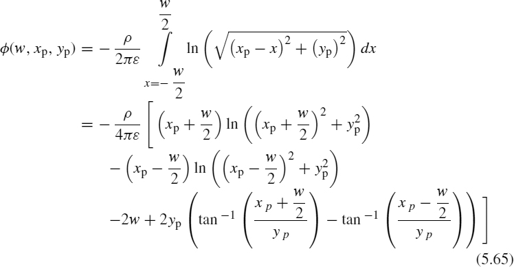
First, we consider solving the problem with the board removed as in Figure 5.21(b) and then we will consider adding the board. Consider the subproblem of a strip of width w representing one of the subsections of a land shown in Figure 5.22. We need to determine the potential at a point a distance d from the strip center and in the plane of the strip. This basic subproblem was solved earlier, and the results of (5.65) and (5.67) specialized to this case are as follows. For a point at the center of the strip, that is, d = 0, the self-potential is given by (5.67):
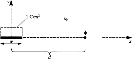
FIGURE 5.22 Illustration of the determination of the potential due to a constant charge distribution on a flat strip via point matching.
For the potential on another segment where d ≠ 0 and generally d > w/2, the potential is
The mutual result in (5.69b) is written in terms of the self term in (5.69a) and the ratio of the subsection separation to subsection width:
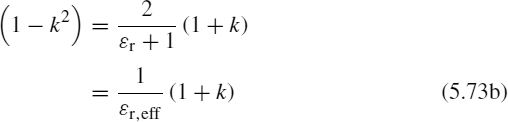
Next consider incorporating the dielectric board into these basic results. The first problem that needs to be solved is that of an infinite (in the z direction) line charge of q C/m situated at a height h above the plane interface between two dielectric media as shown in Figure 5.23. The upper half space has free-space permittivity ε0, and the lower half space has permittivity ε = εr ε0. This classic problem allows one to compute the potential in each region by images in the same fashion as though the lower region were a perfect conductor [1, 9]. The solution can be obtained by visualizing lines of electric flux density, ψ, enamating from the line charge. For an infinite line charge carrying a per-unit-length charge density of q C/m, the electric flux density at a distance r from the line charge is [A.1]
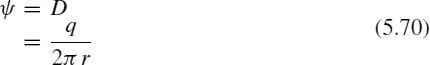
FIGURE 5.23 Illustration of the method of images for a point charge above an infinite dielectric half space.
In a region of permittivity ε, the electric field intensity E is related to D as D = ε E. Consider one such flux line emanating from the line charge that is incident on the interface at some angle θi. Some of this flux can be visualized as passing through the interface as (1 + k)ψ, whereas some is reflected at an angle θr as −kψ. The boundary conditions at the interface require that the normal components of the electric flux density be continuous or
This shows that the angles of incidence and reflection are the same (Snell's law), θi = θr [A.1]. Similarly, the tangential components of the electric field must be continuous across the interface giving

Recalling that θi = θr gives
and
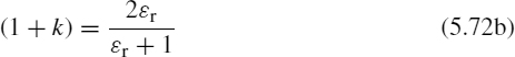
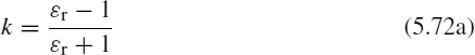
We will find the following combinations of k arising later:
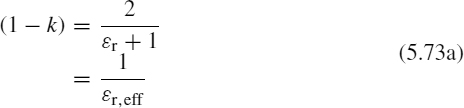
and
and
We have written (5.73) in terms of an effective relative permittivity, (εr + 1)/2. This would be the effective permittivity for the half space in Figure 5.23 as the average of the two permittivities.
FIGURE 5.24 Solution for the potential in each half space in Figure 5.23.
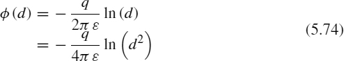
The potential in each half space can be determined as two complementary problems illustrated in Figure 5.24. The potential in a region of permittivity ε at a distance d from an infinite line charge bearing a charge distribution of q C/m is [A.1]
This omits the reference potential. The potential in the upper half space (y > 0) is as though it were due to the original charge q at the original height h and an image charge –kq with the dielectric removed and at a distance h below the interface as shown in Figure 5.24(a):

The potential below the interface (y < 0) is computed as though it is due to a line charge (1 + k)q located at a height h above the interface with the upper free-space region replaced by the dielectric as shown in Figure 5.24(b):

The problem of imaging across a dielectric boundary can be visualized as reflection of the electric flux density vector at the interface similar to optics as shown in Figure 5.25. For a source in the region of permittivity ε0 crossing a boundary into a region of permittivity εrε0 as shown in Figure 5.25(a), the reflected and transmitted electric flux densities are as shown. On the contrary, for a source in the region of permittivity εrε0 crossing a boundary into a region of permittivity ε0 as shown in Figure 5.25(b), the reflected and transmitted electric flux densities are as shown. The reflected ray is the incident ray, instead of being multiplied by −k is multiplied by k. The transmitted ray is the incident ray, instead of being multiplied by (1 + k) is multiplied by (1 − k). Hence, for the case of two dielectric boundaries representing a PCB dielectric substrate such as shown in Figure 5.26, we can easily successively image across both boundaries using this idea. This then gives an infinite set of images.
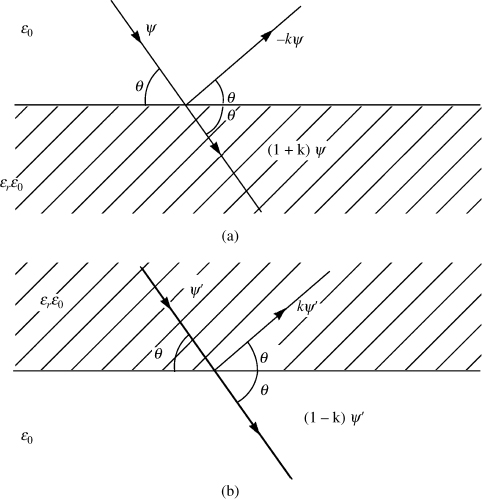
FIGURE 5.25 Solution of the half-space dielectric problem in Figure 5.23 in terms of fluxes.
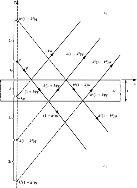
FIGURE 5.26 Images of a point charge above a dielectric slab of finite thickness.
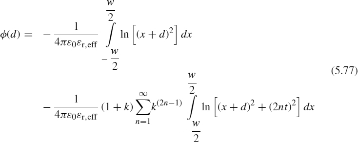
The problem now of interest for the PCB is a line charge on the surface of a dielectric slab (the PCB board) of relative permittivity εr and thickness t shown in Figure 5.27(a). We wish to find the potential at a point on the board at a distance d from the line charge. Specializing the results of Figure 5.26 for h = 0 gives the images shown in Figure 5.27(b) where, for the purposes of computing the potential above the board, the board is replaced with free space. Utilizing 5.74, the potential then is of the form of a series:
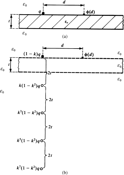
FIGURE 5.27 Illustration of the replacement of a dielectric slab of finite thickness with images to be used in modeling a PCB.
and we have replaced items with those given in 5.73. This series converges rapidly as
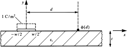
FIGURE 5.28 Illustration of the determination of the per-unit-length capacitances for a PCB by point matching.
Applying this result for a line charge to a infinitesimally thin strip on a dielectric slab by representing the charge distribution (pulse expansion function) as a set of 1 C/m line charges as shown in Figure 5.28 requires performing the following integral:
For a point at the center of the strip, that is, d = 0, the self-potential is given by
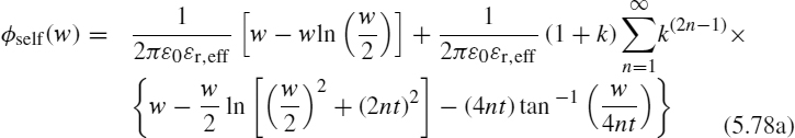
For the potential on another segment where d ≠ 0 and generally d > w/2, the potential is
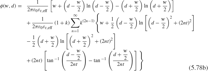
These results can be simplified and written as
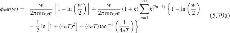
and
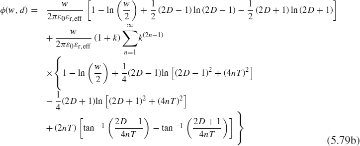
The results have been written in terms of the ratios of the subsection separation to subsection width, D, and board thickness to land width, T:
and
Recall that
denotes the effective dielectric constant as the board thickness becomes infinite, t → ∞, such that it fills the lower half space so that half the electric field lines would exist in air and the other half in the infinite half space occupied by the board. These results are used in the FORTRAN program PCB.FOR described in Appendix A to compute the entries in the per-unit-length capacitance matrix C of a PCB. The per-unit-length inductance matrix L is computed with the board removed from the basic relationship derived earlier:
where C0 is the per-unit-length capacitance matrix with the board removed.
As an example consider the three-conductor PCB shown in Figure 5.29 consisting of three conductors of equal width w and identical edge-to-edge separations s. The following computed results are obtained with the FORTRAN program PCB.FOR (pulse expansion functions and point matching). The results will be computed for typical board parameters: εr = 4.7 (glass epoxy), t = 47 mils, w = s =10 mils. Choosing the left-most conductor as the reference conductor, Figure 5.30(a) compares the elements of the per-unit-length inductance matrix L, Figure 5.30(b) compares the elements of the per-unit-length capacitance matrix C, and Figure 5.30(c) compares the elements of the per-unit-length capacitance without the board, C0, computed for various numbers of land subdivisions. Observe that convergence is achieved for about 20–30 subdivisions of each land. As a check on these results, observe that L22 > L11 as it should be since the loop area between the reference conductor and the second conductor is larger than the loop area between the reference conductor and the first conductor. Similarly, in the capacitance plots observe that C11 > C22 and C011 > C022 since the first conductor is closer to the reference conductor. Figure 5.31 shows the convergence for the capacitances for various numbers of land subdivisions with, C, and without, C0, the board. If one takes the ratios of the corresponding capacitance with and without the board, we see that the effective relative dielectric constant is on the order of 2.6–2.8 for this land width, land separation, and board thickness. This is on the order of the effective dielectric constant
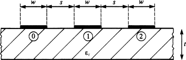
FIGURE 5.29 A PCB consisting of identical conductors with identical separations for the computation of numerical results.
![]()
if the board occupied the infinite half space such that half the electric field lines would reside in free space and the other half in the board. We would expect this to be the case for (a) moderately thick boards and (b) closely spaced lands. For wide land separations, more of the electric field lines exit the bottom of the board and are more important than for closely spaced lands.
There are no known closed-form solutions for this problem, but we may compare the computed results of PCB.FOR to the approximate relations of Chapter 4 for two-conductor PCBs. For example, the results for a two-conductor PCB are given in Eqs. (4.109) of Chapter 4. For example, consider a two-conductor PCB having εr = 4.7, w = s = 15 mils and t = 62 mils. Equations (4.109) give l = 0.804 μH/m and c=38.53 pF/m. PCB.FOR using 30 divisions per land gives l = 0.809μH/m and c = 38.62 pF/m, a difference of 0.2–0.6%. For a PCB having εr = 4.7, w = s = 5 mils and t = 47 mils, the formulas in (4.109) of Chapter 4 give l=0.804 μH/m and c = 39.06 pF/m, whereas PCB.FOR using 30 divisions per land gives l = 0.809 μH/m and c = 39.07 pF/m, a difference of 0.03–0.6%.
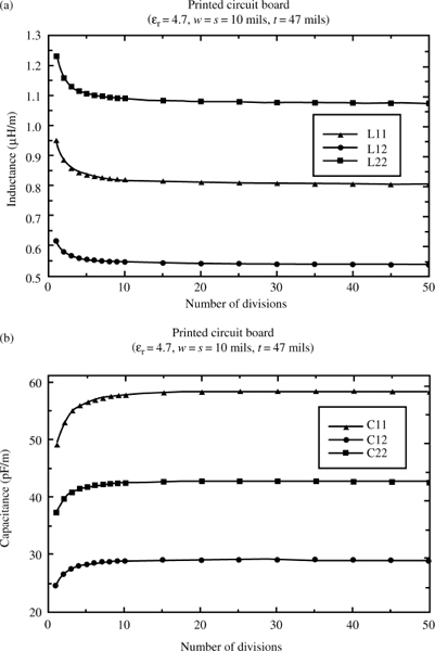
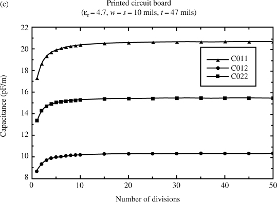
FIGURE 5.30 Illustration of the per-unit-length (a) inductances, (b) capacitances, and (c) capacitances with the board removed for various numbers of divisions of each land for εr = 4.7, land width = separation = 10 mils, and board thickness = 47 mils.
And finally, we will compute the entries in C and L for a PCB that will be used in later crosstalk analyses: εr = 4.7 (glass epoxy), t = 47 mils, w = 15 mils, and s = 45 mils. This separation is such that exactly three lands could be placed between any two adjacent lands. The results for the pulse expansion function, point matching method for 50 divisions per land computed using PCB.FOR are
5.3.1.2 Applications to Coupled Microstrip Lines
Next, we consider applying this technique to the coupled microstrip consisting of lands (of zero thickness) on a dielectric substrate of thickness t and relative permittivity εr with an infinite ground plane on the other side shown in Figure 5.32. The ground plane will serve as the reference or zeroth conductor so that the computation of the generalized capacitance matrix will not be necessary for this case: We directly compute the transmission-line capacitance matrix with the dielectric present, C, and with the dielectric removed, C0. This is implemented in the FORTRAN computer code MSTRP.FOR described in Appendix A. We will assume that all lands are of equal width, w, and edge-to-edge separation, s. Although only three lands are shown, the code will handle any number of lands with the appropriate dimensioning of the arrays in MSTRP.FOR. This problem will represent a PCB with innerplanes, that is, the outer surface of the PCB and the underlying innerplane.
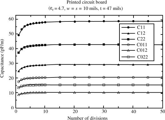
FIGURE 5.31 Comparison of the capacitances with and without the dielectric board versus the number of divisions per land from Figure 5.30(b) and (c).
The first and most basic subproblem we must address is the case of an infinitely long (in the z direction) filament carrying a per-unit-length charge of q C/m on the surface of the board and the determination of the potential on the board at a distance d away as shown in Figure 5.33(a). The sequence of images is shown in Figure 5.33(b) with their sequence number shown. With regard to Figures 5.25 and 5.26, we start with the original charge q and its image across the upper surface that gives a total of (1 − k) q on the surface of the dielectric with that removed. Then, we image this across the ground plane in order to remove the ground plane giving the second image of − (1 − k) q located at a distance t below the original position of the ground plane or a distance 2t below the first charge. Next, we image this charge across the upper surface of the dielectric according to Figure 5.25(b) by multiplying by k to give an image charge of −k (1 − k) q located at a distance of 2t above the dielectric surface. Then, this is imaged across the ground plane to give an image charge of k (1 − k) q located at a distance 3t below the ground plane or a distance of 4t below the first charge. Successive imaging across the ground plane and the dielectric gives the sequence of image charges shown in Figure 5.33(b). This allows the computation of the potential on the surface of the dielectric at a distance d from the original charge with the dielectric and the ground plane removed. Hence, we have the simple problem of computing the potential of an infinite set of line charges in free space. The basic potential for each of these is
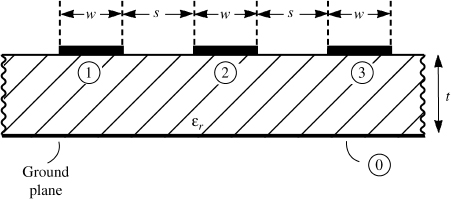
FIGURE 5.32 The three-conductor coupled microstrip line with equal land widths and separations.
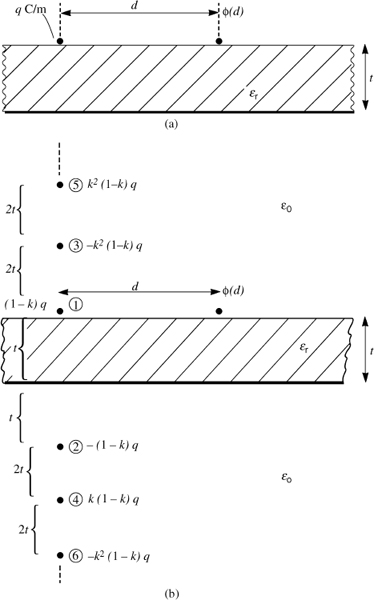
FIGURE 5.33 Determination of (a) the potential on a microstrip due to a line charge by (b) imaging across the boundaries.
Applying this to the sequence of images in Figure 5.33(b) gives
This can be written as
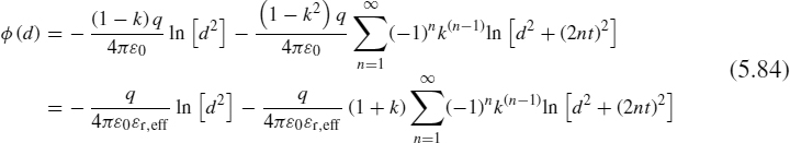
where we have substituted (1 + k)(1 − k) = (1 − k2) and we have written this in terms of the effective dielectric constant where the board thickness goes to infinity, that is, t → ∞:
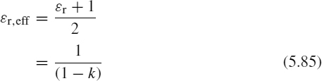
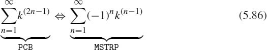
Comparing (5.84) to the same basic subproblem solution for the PCB given in (5.76) shows that we may easily modify the PCB code by simply replacing the summation ![]() in the PCB.FOR program results for the potential with the board present given in (5.78) and (5.79) with
in the PCB.FOR program results for the potential with the board present given in (5.78) and (5.79) with ![]() :
:
Hence, we can make a simple modification of PCB.FOR. In addition, we remove the generalized capacitance calculation from that code as we will be directly computing the transmission-line capacitance matrix since the reference conductor, the ground plane, is already designated.
There is one final but subtle difference. Note that the first term in the summation in (5.84) for n = 1 is nonzero even with the board absent, that is, k = 0. This is the term representing the first image across the ground plane. Hence, the self-potential of a land (d = 0) with the board removed is, from (5.79a) (εr = 1, k = 0),
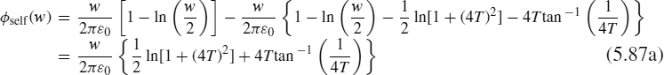
and we have written this in terms of the ratio of dielectric thickness t to land subsection width w:
Similarly, the potential with the board removed but d ≠ 0 and generally d > w/2 becomes, from (5.79b),
and we have written this in terms of (5.88) and the ratio of distance to the potential point, d, to land subsection width w:
The potentials with the board present are obtained from (5.79a) and (5.79b) by substituting (5.86). For the self-potential term, d = 0, we obtain
In reducing this result, we have used the summation (1 − k + k2 − k3 + ···) = 1/(1 + k). For d ≠ 0, the potential becomes, from (5.79b) substituting (5.86),
As an example consider a two-conductor coupled microstrip line consisting of two conductors of equal width w over a ground plane. The following computed results are obtained with the FORTRAN program MSTRP.FOR (pulse expansion functions and point matching). The results will be computed for typical board parameters: εr = 4.7 (glass epoxy), t = 47 mils, and w = s = 10 mils. Figure 5.34(a) compares the elements of the per-unit-length inductance matrix L, Figure 5.34(b) compares the elements of the per-unit-length capacitance matrix C, and Figure 5.34(c) compares the elements of the per-unit-length capacitance without the board, C0, computed for various numbers of land subdivisions. Observe that convergence is achieved for about 20–30 subdivisions of each land. Also observe that the capacitances on the main diagonal of C and C0, C11 and C22 as well as C011 and C022, are equal as they should be by symmetry. Similarly, L11 = L22 as should be the case by symmetry. Figure 5.35 shows the convergence for the capacitances for various numbers of land subdivisions. If one takes the ratios of the corresponding capacitance with and without the board, we see that the effective relative dielectric constant is on the order of 2.6–3.1 for this land width, land separation, and board thickness. This is on the order of the effective dielectric constant
![]()
if the board occupied the infinite half space such that half the electric field lines would reside in free space and the other half in the board. We would expect this to be the case for (a) moderately thick boards and (b) closely spaced lands. For wide land separations, more of the electric field lines will be influenced by the ground plane at the bottom of the board and are more important than for closely spaced lands.
We may compare the computed results of MSTRP.FOR to the approximate relations of Chapter 4. For example, the results for a microstrip line consisting of one land of width w above a ground plane are given in Eqs. (4.108) of Chapter 4. For example, consider a microstrip line having εr = 4.7, w = 5 mils, and t = 50 mils. Equations (4.108) give l = 0.8765 μH/m and c = 38.26 pF/m. MSTRP.FOR using 30 divisions per land gives l = 0.879 μH/m and c = 39.03 pF/m, a difference of 0.3–2%. For a microstrip line having εr = 4.7, w = 100 mils, and t = 62 mils, the formulas in (4.108) of Chapter 4 give l = 0.335μ H/m and c = 115.7 pF/m, whereas MSTRP.FOR using 30 divisions per land gives l = 0.336μ H/m and c = 115.2pF/m, a difference of 0.3–0.4%.
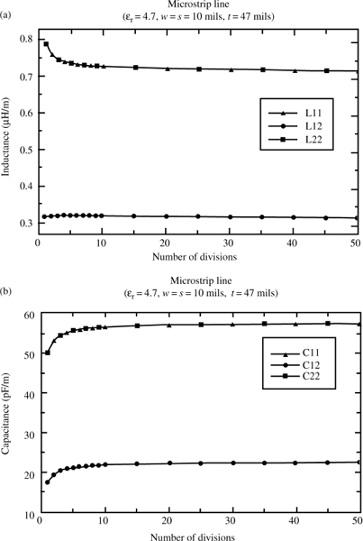
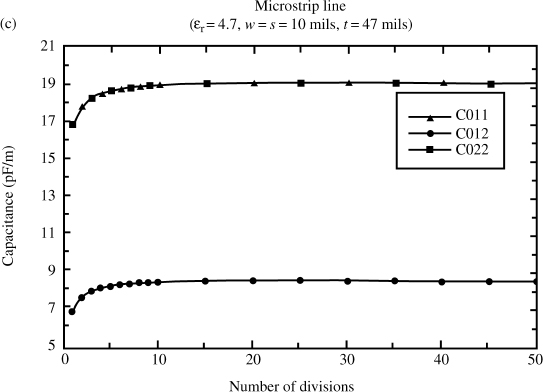
FIGURE 5.34 Determination of (a) inductances, (b) capacitances, and (c) capacitances with the board removed for a two-conductor coupled microstrip with εr = 4.7, land width = separation = 10 mils, and board thickness = 47 mils.
And finally, we will compute the entries in C and L for a coupled microstrip line that will be used in later crosstalk analyses: εr = 4.7 (glass epoxy), t = 62 mils, w = 100 mils, and s =100 mils. The results for the pulse expansion function, point matching method for 50 divisions per land computed using MSTRP.FOR are
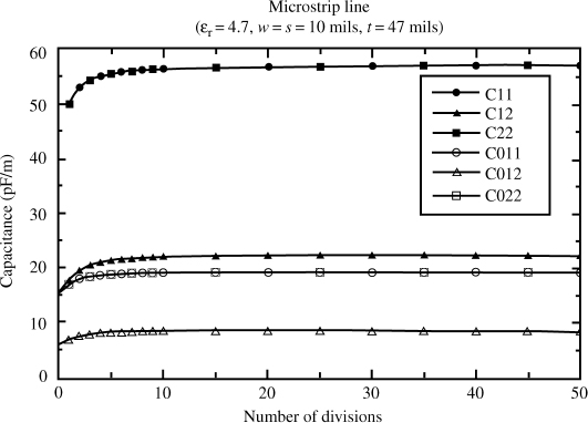
FIGURE 5.35 Comparison of the capacitances with and without the dielectric board versus the number of divisions per land from Figure 5.34 (b) and (c).
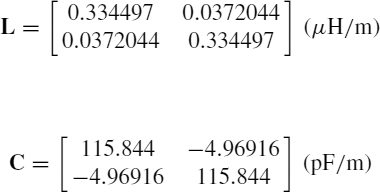
5.3.1.3 Applications to Coupled Striplines
Next, we consider applying this technique to the coupled stripline consisting of lands (of zero thickness) embedded in a dielectric substrate of thickness t and relative permittivity εr with infinite ground planes on both sides as shown in Figure 5.36. The ground planes will serve as the reference or zeroth conductor so that the computation of the generalized capacitance matrix will not be necessary for this case: We directly compute the transmission-line capacitance matrix with the dielectric present, C, and with the dielectric removed, C0. This is implemented in the FORTRAN computer code STRPLINE.FOR described in Appendix A. We will assume that all lands are of equal width, w, with equal edge-to-edge separations, s, and the lands are located midway between the ground planes. Although only three lands are shown, the code will handle any number of lands with the appropriate dimensioning of the arrays in STRPLINE.FOR. This problem will represent a PCB with innerplanes where lands are buried between the innerplanes.
The first and most basic subproblem we must address is the case of an infinitely long (in the z direction) filament carrying a per-unit-length charge of 1 (C/m) located midway between the ground planes, and we need to determine the potential at a point also midway between the ground planes and a distance d from the line charge as shown in Figure 5.37(a). This is a somewhat canonical problem that is solved in Collin [6] and Smythe [1]. The potential specialized to this case is [6].
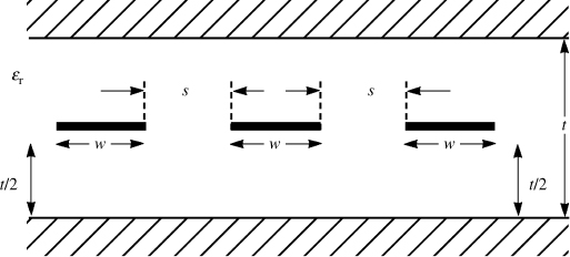
FIGURE 5.36 The three-conductor coupled stripline with equal land widths and separations.
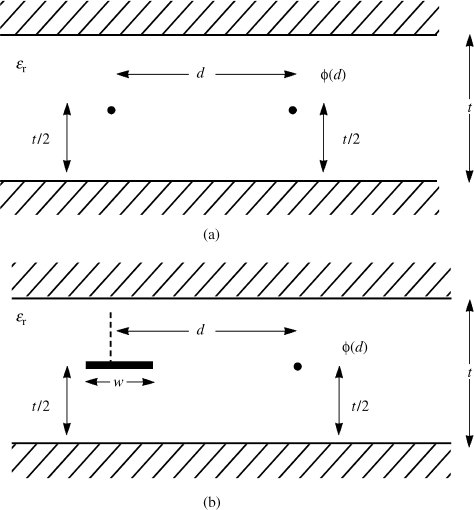
FIGURE 5.37 Illustration of the basic determination of the potential of a stripline for (a) a line charge and (b) a land with constant charge distribution.
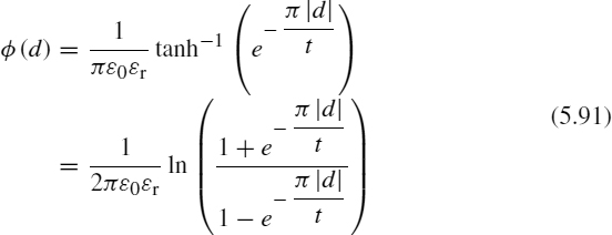
Smythe also gives an equivalent form as
The final subproblem is a strip of zero thickness and width w carrying a charge distribution of 1 C/m2 shown in Figure 5.37(b). The strip is parallel to the ground planes and is located midway between them. The desired potential is located midway between the planes and is a distance d from the midpoint of the strip. Treating the strip as a sequence of charge filaments 1dx (C/m), we sum the contributions to the potential as
This can be integrated by making a change of variables as u = e−(πd/t) e(πx/t) so that du = (π/t)u dx. Substituting into (5.93) gives
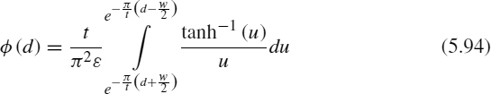
This integrates to (see Dwight [7] integral 735.1)
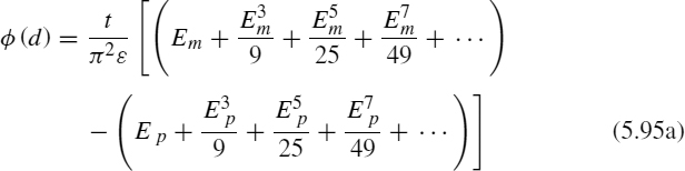
where
and
Each of these two series converges rapidly as for a match point on another strip, d > w/2. For the case where the match point is at the center of the charge-bearing strip, that is, d = 0, we require
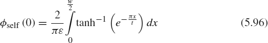
This may also be integrated by making the substitution u = e−(πx/t) and du = −(π/t)u dx to give
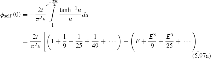
where
Again, both series converge rapidly and the first series converges to (see Dwight [7] #48.12)
We can essentially adapt the program MSTRP.FOR directly to this case by simply changing the computation subroutine for determining ![]() (d) and
(d) and ![]() (0) to the above results.
(0) to the above results.
As an example, consider the coupled stripline consisting of two conductors between ground planes where t = 47 mils, w = s =10 mils, and εr = 4.7. The results obtained with STRPLINE.FOR are shown in the following figures. Figure 5.38(a) compares the elements of the per-unit-length inductance matrix L and Figure 5.38(b) compares the elements of the per-unit-length capacitance matrix, C, computed for various numbers of land subdivisions. It is not necessary to show the corresponding results with the board replaced by free space, C0, since for this homogeneous medium C = εrC0. Observe that convergence is achieved for about 20–30 subdivisions of each land. Also observe that the capacitances on the main diagonal of C, C11 and C22, are equal as they should be by symmetry. Similarly, L11 = L22 as should be the case by symmetry.
We may compare the computed results of STRPLINE.FOR to the approximate relations of Chapter 4. For example, the results for a stripline line consisting of one land of width w midway between the ground planes are given in Eqs. (4.107) of Chapter 4. For example, consider a stripline line having εr = 4.7, w = 5 mils, and t = 50 mils. Equations (4.107) give l = 0.6566μ H/m and c = 79.54 pF/m. STRPLINE.FOR using 60 divisions per land gives l = 0.6515μ H/m and c = 80.27 pF/m, a difference of 0.8–0.9%. For a stripline line having εr = 4.7, w = 5 mils, and t = 10 mils, the formulas in (4.107) of Chapter 4 give l = 0.334μ H/m and c = 156.4 pF/m, whereas STRPLINE.FOR using 60 divisions per land gives l = 0.3362μ H/m and c = 155.53 pF/m, a difference of 0.6–0.7%.
FIGURE 5.38 Determination of (a) inductances and (b) capacitances for a two-conductor coupled stripline with εr = 4.7, land width = separation = 10 mils, and board thickness = 47 mils.
5.4 FINITE DIFFERENCE TECHNIQUES
Recall that the entries in the per-unit-length inductance, capacitance, and conductance matrices are determined as a static (dc) solution for the fields in the transverse (x−y) plane. Essentially, the transverse fields are such that the potential in the space surrounding the conductors, ![]() (x, y), again satisfies Laplace's equation in the transverse plane:
(x, y), again satisfies Laplace's equation in the transverse plane:
FIGURE 5.39 The finite-difference grid.

Finite-difference techniques approximate these spatial partial derivatives in a discrete fashion in the space surrounding the conductors. For example, consider the closed region shown in Figure 5.39. The space is gridded into cells of length and width h. First-order approximations to the first partial derivatives at the interior cell points a, b, c, and d are [A.1,4]
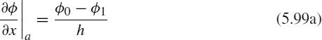
The second-order derivatives are similarly approximated using these results as

This amounts to a central difference expression for the partial derivatives [4]. Substituting these results into (5.98) gives a discrete approximation to Laplace's equation:
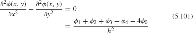
or
Thus, the potential at a point is the average of the potentials of the surrounding four points in the mesh. Equation (5.102) is to be satisfied at all mesh points. Typically, this is accomplished by prescribing the potentials of the mesh points on the conductor surfaces, initially prescribing zero potential to the interior points and then recursively applying (5.102) at all the interior points until the change is less than some predetermined amount at which point the iteration is terminated.
An example of the application of the method is shown in Figure 5.40, which was solved earlier using a MoM method and a direct solution of Laplaces's equation with those results given in Table 5.8. A rectangular box having the four conducting walls at different potentials is shown. The potentials of the interior mesh points obtained iteratively are shown. Observe that, even with this relatively course mesh, the potentials of the mesh points converge rather rapidly.
This method could also be solved in a direct fashion rather than iteratively. Enforcement of the potential via (5.102) at the six interior mesh points gives
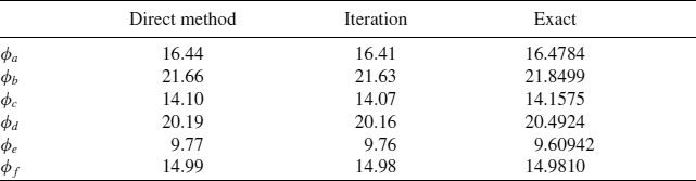
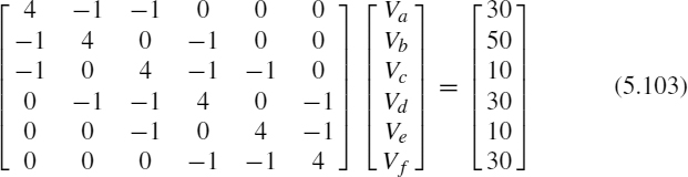
Solving this gives the potentials of the interior mesh points compared to those obtained by iteration in Figure 5.40 as shown in Table 5.8. The exact results were obtained from an analytical solution of Laplace's equation given previously [8].
The solution for the potentials via this method is only one part of the process of determining the per-unit-length generalized capacitance matrix. In order to compute the generalized capacitance matrix, we need to determine the total charge on the conductors (per unit of line length). To implement this calculation, recall Gauss's law:
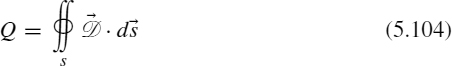
that provides that the charge enclosed by a surface is equal to the integral of the normal component of the electric flux density vector over that surface. For a linear, homogeneous, isotropic medium,
where ![]() is the unit vector normal to the surface. In order to apply this to the problem of computing the charge on the surface of a conductor, consider Figure 5.41. Applying (5.104) and (5.105) to a strip along the conductor surface between the conductor and the first row of mesh points just off the surface gives
is the unit vector normal to the surface. In order to apply this to the problem of computing the charge on the surface of a conductor, consider Figure 5.41. Applying (5.104) and (5.105) to a strip along the conductor surface between the conductor and the first row of mesh points just off the surface gives
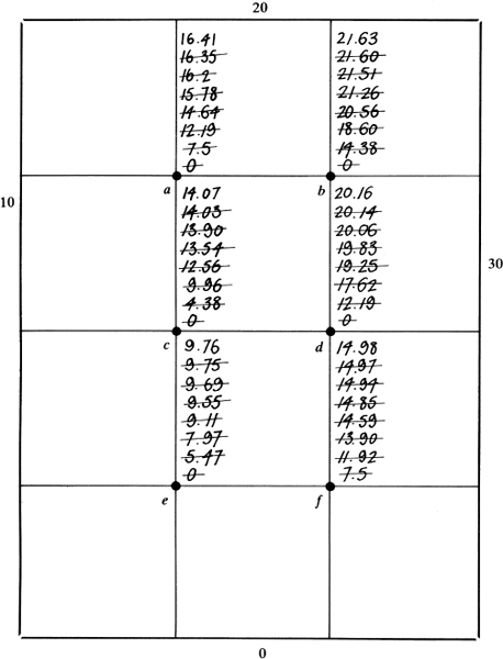
FIGURE 5.40 Example for illustration of the finite-difference method.
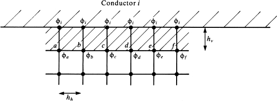
FIGURE 5.41 Use of the finite-difference method in determining surface charge on a conductor.
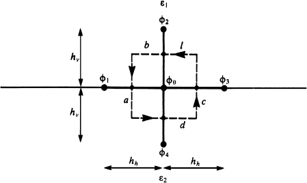
FIGURE 5.42 Illustration of the implementation of the finite-difference method for multiple dielectrics.
Using the potentials computed at the interior mesh points, we can obtain the charge on the surface by applying (5.106) in discrete form as
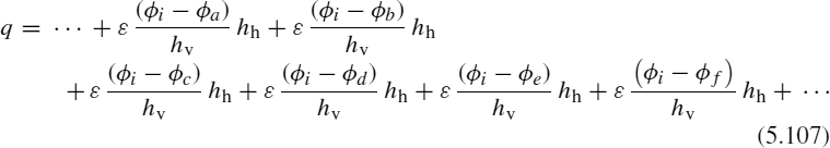
where hv denotes the “vertical” length of the mesh perpendicular to the conductor surface and hh denotes the “horizontal” length of the mesh parallel to the conductor surface. Once the charges on the conductors are obtained in this fashion, the generalized capacitance matrix can be formed and from it the per-unit-length capacitances can be obtained.
Dielectric inhomogeneities can be handled in a similar fashion with this method. Gauss's law requires that, in the absence of any free charge intentionally placed at an interface between two dielectrics, there can be no net charge on the surface. Consider the interface between two dielectrics shown in Figure 5.42, where a mesh has been assigned at the boundary. Applying Gauss's law to the surface surrounding the center point of the mesh shown as a dashed line gives
Finite-difference methods are particularly adapted to closed systems. For open systems where the space extends to infinity in all directions, a method must be employed to terminate the mesh. A rather simple but computationally intensive technique is to extend the mesh to a large but finite distance from the conductors and terminate it in zero potential. To check the sufficiency of this, extend the mesh slightly larger and recompute the results.
5.5 FINITE-ELEMENT TECHNIQUES
The third important numerical method for solving (approximately) Laplace's equation is the finite-element method or FEM. The FEM approximates the region and its potential distribution by dividing the region into subregions (finite elements) and representing the potential distribution over that subregion. We will restrict our discussion to the most commonly used finite element, the triangle surface shown in Figure 5.43(a). Higher order elements are discussed in [4,9]. Figure 5.43(b) illustrates the approximation of a 2D region using these triangular elements. The triangle element has three nodes at which the potentials are prescribed (known). The potential distribution over the element is a polynomial approximation in the x, y coordinates:
Evaluating this equation at the three nodes gives
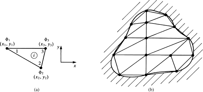
FIGURE 5.43 Illustration of (a) the finite-element triangular element and (b) its use in representing two-dimensional problems.
Solving this for the coefficients gives
where

and the area of the element is
Observe the cyclic ordering of the subscripts in (5.111) as 1 → 2 → 3. Given the node potentials, the potential at points on the element surface can be found from (5.109) using (5.111) and (5.112). The electric field over the surface of the element is constant:
Observe that when a surface is approximated by these triangular elements as in Figure 5.43(b), the potential is guaranteed to be continuous across the common boundaries between any adjacent elements.
The key feature in insuring a solution of Laplace's equation by this method is that the solution is such that the total energy in the field distribution in the region is a minimum [4, 9]. The total energy in the system is the sum of the energies of the elements:
The minimum energy requirement is that the derivatives with respect to all free nodes (nodes where the potential is unknown) are zero:
The energy of the ith element is
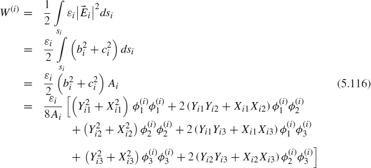
where ![]() is the potential of node k (k = 1, 2, 3) for the ith element. This can be written in matrix notation as a quadratic form as
is the potential of node k (k = 1, 2, 3) for the ith element. This can be written in matrix notation as a quadratic form as
where
and superscript t denotes transpose. The matrix
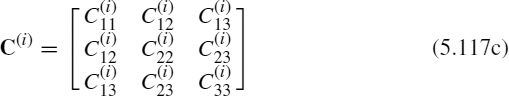
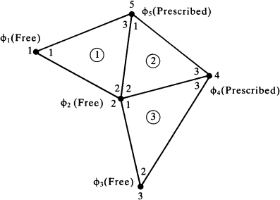
FIGURE 5.44 An example to illustrate the use of the FEM.
is referred to as the local coefficient matrix with entries
Now, we must assemble the total energy expression for a system that is approximated by finite elements according to (5.114). In order to illustrate this, consider the example of a region that is represented by three finite elements shown in Figure 5.44. The node numbers inside the elements are the local node numbers as used above. The global node numbers are shown uniquely for the five nodes. Nodes 1, 2, and 3 are free nodes whose potential is to be determined to satisfy Laplace's equation in the region. Nodes 4 and 5 are prescribed nodes whose potentials are fixed (known). The total energy expression can be written in terms of the global nodes as
where the vector of global node potentials is
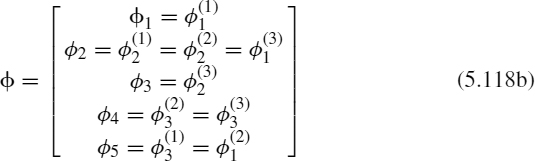
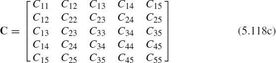
This global coefficient matrix C, like the local coefficient matrix, can be shown to be symmetric by energy considerations [9]. The entries in the global coefficient matrix can be assembled quite easily from the local coefficient matrix (whose entries are computed for the isolated elements independent of their future connection) with the following observation. For each element write the global coefficient matrix as
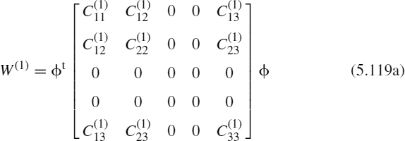
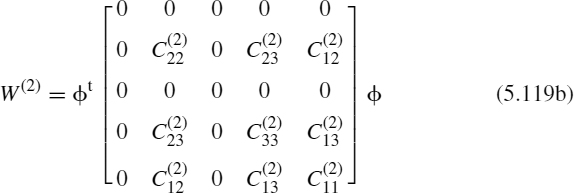
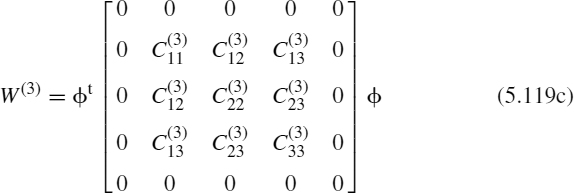
Assembling these according to (5.118) gives the total energy
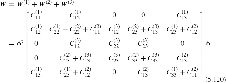
A very simple rule for assembling this global coefficient matrix can be developed from this example. The main diagonal terms are the sums of the main diagonal terms of the local coefficient matrices for those elements that connect to this global node. The off-diagonal terms are the sums of the off-diagonal terms of the local coefficient matrices whose sides connect the two global nodes. Observe that the off-diagonal terms will have at most two entries, whereas the main diagonal terms will be the sum of a number of terms equal to the number of elements that share the global node.
Now it remains to differentiate this result with respect to the free nodes to insure minimum energy of the system thereby satisfying Laplace's equation. To that end, let us number the global nodes by numbering the free nodes first and then numbering the prescribed (fixed potential) nodes last. The above energy expression can then be written in partitioned form as
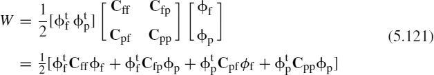
Differentiating this with respect to the free node potentials and setting the result to zero gives the final equations to be solved:
Solving this matrix equation for the free node potentials is referred to as the direct method of solving the FEM equations.
Observe from the example of Figure 5.44 that the global coefficient matrix C has a number of zero entries. This is quite evident as only those (two) elements that contain the nodes for this entry will contribute a nonzero term. Thus, the coefficient matrices in (5.122) will be sparse. Although there exist sparse matrix solution routines that efficiently take advantage of this, FEM problems, particularly large ones, are generally solved more efficiently using the iterative method. This is similar to the iterative method for the finite-difference technique in that the free nodes are initially prescribed some starting value (such as zero) and the new values of the free node potentials are computed. The process continues until the change in the free node potentials between iteration steps is less than some value. Writing out (5.122) for the example of Figure 5.44 gives
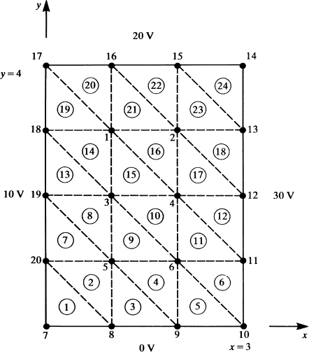
FIGURE 5.45 Illustration of the FEM applied to a previously solved problem.
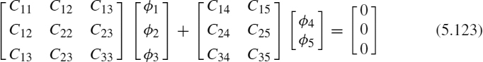
Writing this in terms of each free potential with respect to the other free potentials and the prescribed potentials gives
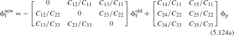
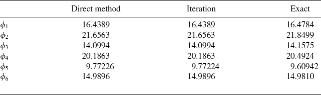
where
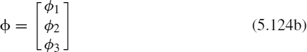
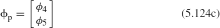
As a numerical illustration of the method, consider the problem of a rectangular region of side lengths 4 and 3 with prescribed potentials of 0 V, 10 V, 20 V, and 30 V as shown in Figure 5.20. This was solved earlier with the MoM technique and the finite-difference technique. In order to compare this with the finite-difference technique, we will again choose six interior nodes and approximate the space between these nodes with 24 finite elements as shown in Figure 5.45. Observe that the potentials at nodes 7, 10, 14, and 17 are not known since there are gaps between the adjacent conductors. We will prescribe these potentials as the average of the adjacent conductor potentials or 5 V, 15 V, 25 V, and 15 V. The solution for the six interior node potentials via the direct and the iterative method become as shown in Table 5.9. The iterative method converged after 15 iterations.
Some of the important features of the FEM are that it can handle irregular boundaries as well as inhomogeneous media. Inhomogeneous media are handled by ensuring that the region is subdivided such that each finite element covers (approximately) a homogeneous subregion. The permittivities of the finite elements, εi, are contained in the ![]() local node coefficients.
local node coefficients.
Once again, as with the finite-difference method, the finite-element method is most suited to closed systems. For open systems whose boundaries extend to infinity, an infinite mesh method can be developed [4] or the mesh can be extended sufficiently far from the main areas of interest and artificially terminated in zero potential thereby forming a (artificial) closed system.
The FEM is a highly versatile method for solving Laplace's equation as well as other electromagnetic fields problems [4, 9]. Other parameters of interest such as capacitances can be determined in the usual fashion by determining the resulting charge on the conductors as the normal component of the displacement vector just off the conductor surfaces.
PROBLEMS
5.1 Demonstrate the generalized capacitance relations in (5.21).
5.2 Show the result in (5.22).
5.3 Demonstrate the result in (5.23) for (n + 1) widely spaced wires.
5.4 Determine the per-unit-length inductances for a three-wire ribbon cable where the center wire is chosen as the reference conductor. [l11 = l22 = (μ0/π)ln(d/rw), l12 = (μ0/2π)ln(d/2rw)] Evaluate these for a center-to-center wire spacing of 50 mils and #28 gauge stranded wires having wire radii of rw = 7.5 mils. [l11 = l22 = 0.759μH/m = 19.3nH/in., l12 = 0.24μH/m = 6.1nH/in.]. Determine the per-unit-length capacitances (neglecting the wire insulations) from these. [c11 = c22 = 11.1 pF/m = 0.28 pF/in., c12 = 5.17 pF/m = 0.13 pF/in.]
5.5 Repeat the calculations of problem 5.4 using WIDESEP.FOR. [l11 = l22 = 0.7588μH/m, l12 = 0.2408μ H/m, c11 = c22 = 11.13pF/m, c12 = 5.174 pF/m]
5.6 Demonstrate the relations in (5.25) for n wires above an infinite, perfectly conducting ground plane.
5.7 Determine the per-unit-length inductances for two wires at an equal height above a ground plane and separation s. [l11 = l22 = (μ0/2π)ln(2h/rw), l12 = (μ0/4π)ln(1+4(h2/s2))] Evaluate these for a center-to-center wire spacing of 2 cm, a height of 2 cm and #20 gauge solid wires having wire radii of rw = 16 mils. [l11 = l22 = 0.918μ H/m = 23.3nH/in., l12 = 0.161μ H/m = 4.09nH/in.]. Determine the per-unit-length capacitances (neglecting the wire insulations) from these. [c11 = c22 = 10.3pF/m, c12 = 2.19pF/m]
5.8 Repeat the calculations of problem 5.7 using WIDESEP.FOR. [l11 = l22 = 0.9178μ H/m, l12 = 0.1609μ H/m, c11 = c22 = 10.314 pF/m, c12 = 2.193 pF/m]
5.9 Demonstrate the relations in (5.26) for n wires within an overall shield.
5.10 Determine the per-unit-length inductances for two wires within an overall shield where the wires are #28 gauge stranded having wire radii of rw = 7.5 mils. The wires are separated by 180°, the shield radius is rS = 4rw, and the distance of each wire from the center is two wire radii. This is typical for shielded pairs of wires where the wire insulation thicknesses are equal to the wire radii. [l11 = l22 = 0.22 μH/m, l12 = 44.6nH/m]
5.11 Repeat the calculations of Problem 5.10 using WIDESEP.FOR. [l11 = l22 = 0.2197μ H/m, l12 = 44.63 nH/m, c11 = c22 = 42.1 pF/m, c12 = 10.73 pF/m]
5.12 Demonstrate the results in Table 5.1.
5.13 Demonstrate the results in Tables 5.2 and 5.3.
5.14 Demonstrate the results in (5.48).
5.15 Determine, using RIBBON.FOR, the results in Tables 5.5 and 5.6 for a three-wire ribbon cable consisting of #28 gauge stranded wires (rw = 7.5 mils) with insulation thicknesses of 10 mils and εr = 3.5 and separations of 50 mils but with the center wire chosen as the reference conductor. [l11 = l22 = 0.7485μ H/m, l12 = 0.2408μ H/m, c11 = c22 = 24.98 pF/m, c12 = 6.266 pF/m]
5.16 Demonstrate the relations in (5.65) and (5.67).
5.17 Demonstrate the relations in (5.75) and (5.76).
5.18 Demonstrate the relations in (5.78).
5.19 Determine the per-unit-length inductances and capacitances for a three-conductor PCB having land widths of 25 mils, a board thickness of 30 mils, and an edge-to-edge separation of 10 mils and εr = 4.7 using PCB.FOR. Use 30 divisions per land and choose the reference conductor to be the center land. [l11 = l22 = 0.626μ H/m, l12 = 0.1812μ H/m, c11 = c22 = 38.35 pF/m, c12 = 11.197 pF/m]
5.20 Demonstrate the relations in (5.83).
5.21 Determine the per-unit-length inductances and capacitances for a two-conductor coupled microstrip having land widths of 25 mils, a board thickness of 30 mils, and an edge-to-edge separation of 10 mils and εr = 4.7 using MSTRP.FOR. Use 30 divisions per land and choose the reference conductor to be the center land. [l11 = l22 = 0.4484μ H/m, l12 = 0.1543μ H/m, c11 = c22 = 65.26 pF/m, c12 = 22.92 pF/m]
5.22 Demonstrate the relations in (5.95) and (5.97).
5.23 Determine the per-unit-length inductances and capacitances for a two-conductor coupled stripline having land widths of 25 mils, a separation between the two ground planes of 30 mils, and an edge-to-edge separation of 10 mils and εr = 4.7 using STRPLINE.FOR. Use 30 divisions per land and choose the reference conductor to be the center land. [l11 = l22 = 0.2466μ H/m, l12 = 21.6nH/m, c11 = c22 = 195 pF/m, c12 = 18.72 pF/m]
5.24 Demonstrate the relation for the finite-difference method in (5.102).
5.25 Reproduce the results in Table 5.8 for the finite-difference method.
5.26 Demonstrate the relations in (5.111) for the finite-element method.
5.27 Demonstrate the relation in (5.116) for the finite-element method.
5.28 Reproduce the results in Table 5.9 for the finite-element method.
REFERENCES
[1] W.R. Smythe, Static and Dynamic Electricity, 3rd edition, McGraw-Hill, New York, 1968.
[2] A.T. Adams, Electromagnetics for Engineers, Ronald Press, New York, 1971.
[3] R.F. Harrington, Field Computation by Moment Methods, Macmillan, New York, 1968.
[4] M.N. O. Sadiku, Numerical Techniques in Electromagnetics, CRC Press, Boca Raton, FL, 1992.
[5] W.T. Weeks, Calculation of coefficients of capacitance of multiconductor transmission lines in the presence of a dielectric interface, IEEE Transactions on Microwave Theory and Techniques, 18 (1), 35–43, 1970.
[6] R.E. Collin, Field Theory of Guided Waves, 2nd edition, IEEE Press, New York, 1991.
[7] H.B. Dwight, Tables of Integrals and Other Mathematical Data, 4th edition, Macmillan, New York, 1961.
[8] M.Javid, and P.M. Brown, Field Analysis and Electromagnetics, McGraw-Hill, New York, 1963.
[9] P.P. Sylvestor, and R.L. Ferrari, Finite Elements for Electrical Engineers, 2nd Edition, Cambridge University Press, New York, 1990.