
10
LITERAL (SYMBOLIC) SOLUTIONS FOR THREE-CONDUCTOR LINES
The general solution of the transmission-line equations for a two-conductor line considered in Chapters 6 and 8 is simple enough that it can be obtained in literal form, that is, in terms of symbols for the line terminations and the line parameters such as characteristic impedance ZC and the line one-way time delay TD. For example, see Eqs. (6.39) and (6.70) of Chapter 6 and (8.14) of Chapter 8. This literal or symbolic solution gives considerable insight into how the various parameters affect the terminal voltages and currents. This advantage is similar to a transfer function that is useful in the design and analysis of electric circuits and automatic control systems [A.2]. In order to obtain the same insight from the numerical solution, we would need to perform a large set of computations with these parameters being varied over their range of anticipated values.
Chapters 7 and 9 have examined the solution of the MTL (multiconductor transmission line) equations for a general (n + 1)-conductor line. This is so complex that it is not feasible to generate literal solutions, and the solution process must be accomplished with digital computer programs, that is, a numerical result is obtained. This numerical process does not reveal the general behavior of the solution. In other words, the only information we obtain is the solution for the specific set of input data, for example, line length, terminal impedance levels, source voltages, frequency, and so on. In order to understand the general behavior of the solution for a general (n + 1)-conductor MTL, it would be helpful to have a literal solution for the induced crosstalk voltages in terms of the symbols for the line length, terminal impedances, per-unit-length capacitances and inductances, source voltage, and so on. From such a result we could observe how changes in these parameters would affect the solution. Although highly desirable, such a literal solution is, in general, not feasible.
It is important to keep in mind that even though it may be possible to obtain a literal solution after laboriously manipulating the symbolic equations, any such result is worthless unless the result is simple enough to clearly and easily show what the mathematical result is telling us about the behavior of the system. There exist in the literature several symbolic results that are so complicated that no physical insight can be obtained. Hence, there is little value to going through the laborious symbolic solution, and one can obtain the same information included in these symbolic equations more easily by simply solving the transmission-line equations and incorporating the terminal constraints using numerical computer solutions. Hence, any symbolic result is useful only if it is simple enough to be interpretable.
Several transmission-line literal transfer functions for the prediction of crosstalk have been derived in the past for use in the frequency-domain analysis of microwave circuits [1–4] or for time-domain analysis of crosstalk in digital circuits [5–11]. All of these solutions assume that the line is a three-conductor line, that is, n = 2, with two signal conductors and a reference conductor. In addition, these results make the following assumptions about the line in order to simplify the derivation.
- The line is symmetric, that is, the two signal conductors are identical in crosssectional shape and the cross-sectional line dimensions are such that the self capacitances and inductances are identical, that is, c11 = c22 and l11 = l22. An example is the coupled microstrip where the two identical lands are at the same distance above the ground plane. For this case, the per-unit-length inductance and capacitance matrices are of the form
- The line is weakly coupled, that is, the effect of the induced signals in the receiving circuit on the driven circuit, that is, back interaction, is neglected (widely separated lines tend to satisfy this in an approximate fashion the wider the separation).
- Both lines are matched at both ends, that is, the line is terminated at all four ports in the line characteristic impedances. The question of what is meant by the “line characteristic impedances” for an MTL will need to be clarified. For weakly coupled or widely separated lines, these approximate to the characteristic impedances of the isolated two-conductor lines.
- The line is lossless, that is, the conductors are perfect conductors and the surrounding medium is lossless.
The obvious reason why these assumptions are used is to simplify the difficult manipulation of the symbols that are involved in the literal solution. The assumption of a symmetric line and the subsequent literal solution is referred to in the microwaves literature as the even–odd mode solution [1–3]. However, the vast majority of the applications are not perfectly matched at all four ports. For example, consider a three-conductor line where each line with the reference conductor connects a CMOS driver and a CMOS receiver. The input to a CMOS inverter looks essentially capacitive. Since the characteristic impedances for lossless lines must be purely real, that is, resistive, these lines are severely mismatched at their load ends.
The purpose of this chapter is to derive the literal or symbolic solution of the MTL equations for a three-conductor line and to incorporate the terminal constraints into this solution to yield explicit, symbolic equations for the crosstalk. Both the frequency-domain and the time-domain solutions will be obtained. In addition, the derivations will not presume a symmetric line nor will they presume a “matched” line. The idea is to simply proceed through the usual solution steps that would be involved in a numerical solution but instead to use symbols for all quantities rather than numbers. First, we determine the general solution of the MTL equations for n = 2. This has generally already been done in earlier chapters. However, in order to simplify the solution, we will assume a lossless line, that is, we will assume perfect conductors in a lossless medium, R = 0 and G = 0. Next, we incorporate the terminal constraints into that general solution in order to give the desired literal solution. For a three-conductor line this last step, incorporation of the terminal conditions, involves the simultaneous solution of symbolic equations with, for example, Cramer's rule and is quite tedious. It therefore does not appear to be feasible to extend this symbolic solution to lines consisting of more than three conductors. Even for a three-conductor line, the solution effort is so great that we must make another simplifying assumption. This primary assumption is to assume a homogeneous surrounding medium so that we may take advantage of the important identity for a homogeneous medium, LC = με12. This identity essentially reduces the number of symbols and allows the consolidation of certain other groups of the per-unit-length symbols. Once the exact result has been derived for only the assumption of a lossless line in a homogeneous medium, we will then specialize this exact result to the case of weak coupling between the two circuits. This will verify the widely used approximate model referred to as the inductive–capacitive coupling model [A.3]. The solution for the general case of perfect conductors in a lossless but inhomogeneous medium is obtained in [B.30]. In order for that solution to be feasible to obtain, the assumption of weak coupling must be made at the outset.
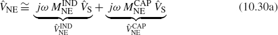
The general statement of the problem is illustrated in Figure 10.1(a). The line consists of three perfect conductors immersed in a lossless medium. The generator circuit is composed of a generator conductor with the reference conductor. It is driven at the left end with an open-circuit source voltage VS(t) and source resistance RS and is terminated at the right end in a load resistance RL. The receptor circuit is composed of a receptor conductor and the reference conductor. It is terminated at the left or “near end” in a resistance RNE and at the right or “far end” in a resistance RFE. Although resistive terminations are used in the following developments, the frequency-domain phasor crosstalk results that we will obtain apply for complex-valued terminal impedances. The per-unit-length equivalent circuit is shown in Figure 10.1(b). From this, the MTL equations can be derived in the usual manner and become

FIGURE 10.1 The three-conductor MTL: (a) line dimensions and terminal characterization and (b) the per-unit-length equivalent circuit.
where


Subscripts G denote quantities associated with the generator circuit, whereas subscripts R denote quantities associated with the receptor circuit. The subscript m denotes the mutual quantity between the two circuits. The generalized Thevenin equivalent characterization of the terminations becomes
where


Although we assume resistive terminations, the frequency-domain solution will allow complex-valued terminations. The objective is to obtain equations for the time-domain near-end and far-end crosstalk voltages: VNE(t) = VR(0, t) and VFE(t) = VR(![]() , t).
, t).
10.1 THE LITERAL FREQUENCY-DOMAIN SOLUTION FOR A HOMOGENEOUS MEDIUM
In order to simplify the solution process, we assume that the surrounding medium is homogeneous and characterized by permittivity ε and permeability μ. Because of the assumption of a homogeneous surrounding medium, we have the important identity
or, by multiplying both sides by L−,
where ![]() is the velocity of propagation of the waves in the homogeneous medium. This identity gives the following relations between the per-unit-length parameters:
is the velocity of propagation of the waves in the homogeneous medium. This identity gives the following relations between the per-unit-length parameters:


The frequency-domain MTL equations for sinusoidal steady-state excitation become

where the phasor line voltages and currents are

The phasor generalized Thevenin equivalent characterization of the terminations becomes
where


The objective is to obtain equations for the phasor near-end and far-end crosstalk voltages: ![]() and
and ![]() .
.
For this special case of perfect conductors in a lossless homogeneous medium, the MTL equations are decoupled as in Section 7.2.2.1 giving
where 12 is the 2 × 2 identity matrix. The general solution of the MTL equations in terms of the chain-parameter matrix for this case becomes
where the chain-parameter submatrices for this case of perfect conductors in a lossless homogeneous medium simplify to (see Eqs. (7.115) of Chapter 7)
where
and the phase constant is
The terminal characterization in (10.9) is substituted into the chain-parameter matrix in (10.12) to give (see Eqs. (7.92) of Chapter 7)
Substituting the chain-parameter submatrices given in (10.13) into (10.15) gives

Each of the equations in (10.16a) and (10.16b) are two simultaneous equations and once they are solved, the near-end and far-end crosstalk voltages are obtained from the second entries in these solution vectors as ![]() and
and ![]()
![]() .
.
Equations (10.16) were solved in [B.6] in literal form via Cramer's rule to yield the following exact literal solutions for the near-end and far-end crosstalk voltages:
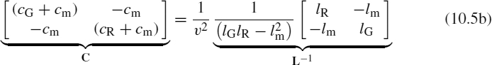
The various quantities in these equations are defined as [B.6]
where the inductive coupling coefficients are defined by


and the capacitive coupling coefficients are defined by

The coupling coefficient between the two circuits is defined by
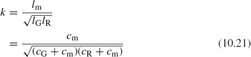
and the circuit characteristic impedances are defined by


where we have substituted (10.21) and the identities from (10.6d) and (10.6e). It should be pointed out that, as was previously determined, the line has a characteristic impedance matrix, and scalar characteristic impedances as defined above have no functional meaning. Here, we are merely defining terms that relate back and reduce to the scalar characteristic impedances of the two-conductor line. Observe that these definitions of each characteristic impedance do not simply involve just the self-capacitances of each circuit, cG and cR, but also contain the mutual capacitance cm as (cG + cm) and (cR + cm). For weakly coupled lines ![]() these do indeed reduce to the scalar characteristic impedances of the isolated lines; ZCG
these do indeed reduce to the scalar characteristic impedances of the isolated lines; ZCG ![]() vlG and ZCR
vlG and ZCR ![]() vlR. The relationships of the termination impedances to their associated characteristic impedances are important parameters. In order to highlight this dependency, the various ratios of termination impedance to the appropriate characteristic impedance are defined by
vlR. The relationships of the termination impedances to their associated characteristic impedances are important parameters. In order to highlight this dependency, the various ratios of termination impedance to the appropriate characteristic impedance are defined by
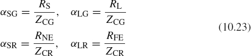
The remaining quantities are defined in the following way. The coefficient KNE in (10.17) is defined by

If only one line is matched at its load end, that is, αLG = 1 or αLR = 1, then ![]()
![]() and for a weakly coupled line,
and for a weakly coupled line,![]() , KNE
, KNE ![]() 1. The circuit time constants are logically defined as
1. The circuit time constants are logically defined as


and the line one-way delay is denoted as
and ![]() for this homogeneous medium. If a line is matched at only one end, its time constant reduces to
for this homogeneous medium. If a line is matched at only one end, its time constant reduces to ![]() . In other words,
. In other words, ![]() if αSi = 1 or if αLi = 1. In addition, if the line is weakly coupled,
if αSi = 1 or if αLi = 1. In addition, if the line is weakly coupled, ![]() , the time constant reduces to τi
, the time constant reduces to τi ![]() TD.
TD.
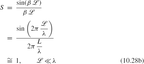
In terms of the ratios in (10.23), the factor P in Den in (10.17c) becomes

The coupling coefficient is always less than unity, that is, k < 1. Hence, P ![]() 1 if the line is weakly coupled,
1 if the line is weakly coupled, ![]() . There is another important case where P is identically unity, P = 1, and that occurs when the lines are matched at opposite ends, that is, αSG = αLR = 1 or αLG = αSR = 1, which occurs in directional couplers [1]. Hence, for these cases, the denominator of the expression in (10.17c) factors as
. There is another important case where P is identically unity, P = 1, and that occurs when the lines are matched at opposite ends, that is, αSG = αLR = 1 or αLG = αSR = 1, which occurs in directional couplers [1]. Hence, for these cases, the denominator of the expression in (10.17c) factors as
![]()
10.1.1 Inductive and Capacitive Coupling
The above results are an exact literal solution for the problem. No assumptions about symmetry or matched loads are used. Therefore, they cover a wider class of problems than have been considered in the past. Although they have been simplified by defining certain terms, they can be simplified further if we make the following assumptions. First, let us assume that the line is electrically short at the frequency of interest, that is, ![]() . In this case, the terms C and S simplify to
. In this case, the terms C and S simplify to

Further, let us assume that Den ![]() 1 in (10.17c). This will be the case for a weakly coupled line, that is,
1 in (10.17c). This will be the case for a weakly coupled line, that is, ![]() , such that P in (10.27) is approximately unity, P
, such that P in (10.27) is approximately unity, P ![]() 1, and a sufficiently small frequency such that Den
1, and a sufficiently small frequency such that Den ![]() 1 in (10.17c). Under these assumptions, the exact results in (10.17) simplify to
1 in (10.17c). Under these assumptions, the exact results in (10.17) simplify to

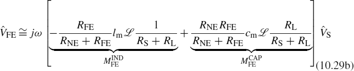
These low-frequency results can be computed from the equivalent circuit of Figure 10.2(a). The terms depending on the per-unit-length mutual inductance lm are referred to as the inductive coupling contributions, whereas the terms depending on the per-unit-length mutual capacitance cm are referred to as the capacitive coupling contributions.

FIGURE 10.2 The frequency-domain inductive-capacitive low-frequency coupling model.
Observe that the low-frequency approximate results in (10.29) show that the crosstalk varies directly with frequency or 20 dB/decade as illustrated in Figure 10.2(b). The total coupling can be written as the sum of inductive coupling and capacitive coupling components as

Depending on the levels of the load impedances, the inductive coupling contribution may dominate the capacitive coupling contribution, or vice versa. This is illustrated in Figure 10.3. If the termination impedances are much smaller than the line characteristic impedances, that is, low-impedance loads, then inductive coupling dominates. This is shown by substituting (10.19) and (10.20) into ![]() and
and ![]() to yield
to yield

FIGURE 10.3 Illustration of the dominance of (a) inductive coupling for low-impedance terminations and (b) capacitive coupling for high-impedance terminations.


We have written this result in terms of the line characteristic impedances by substituting the identity in (10.6f) along with (10.21) into (10.22). On the contrary, capacitive coupling dominates in the case of high-impedance loads, that is, ![]() and
and ![]() . Thus, capacitive coupling dominates inductive coupling when the inequalities in (10.31) are reversed, that is, for high-impedance loads.
. Thus, capacitive coupling dominates inductive coupling when the inequalities in (10.31) are reversed, that is, for high-impedance loads.
Although this approximation is valid only for a line that is electrically short and for a sufficiently small frequency, this separation of the total coupling into an inductive coupling and a capacitive coupling component provides considerable understanding of the crosstalk phenomena. In particular, it readily explains how shields and/or twisted pairs of wires will or will not reduce crosstalk [A.3].
10.1.2 Common-Impedance Coupling
The above derivation assumes that all three conductors are perfect conductors and the surrounding homogeneous medium is lossless. Losses can be ignored in many practical problems. However, there is a potentially significant contribution to crosstalk via imperfect conductors that occurs at the lower frequencies. This is referred to as common-impedance coupling and is contributed by the impedance of the reference conductor.
FIGURE 10.4 Illustration of common-impedance coupling due to a lossy reference conductor.
Figure 10.4 illustrates the problem. As the frequency of excitation is lowered, the crosstalk decreases directly with frequency. At some lower frequency, this contribution due to the electric and magnetic field interaction between the two circuits is dominated by the common-impedance coupling component. At a sufficiently low frequency, the current in the generator circuit, ÎG, returns predominantly in the reference conductor and can be computed from

If we lump the per-unit-length resistance of the reference conductor, r0, as a total resistance, R = r0![]() , then a voltage drop of
, then a voltage drop of

is developed across the reference conductor. This is voltage divided across the termination resistors of the receptor circuit to give

In an approximate sense, we may simply combine these contributions with the inductive–capacitive coupling contributions in (10.30) to give the total as

This approximate inclusion of the impedance of the reference conductor at low frequencies was verified in [B.20] by deriving the exact chain-parameter matrix with the per-unit-length resistance of the reference conductor included.
10.2 THE LITERAL TIME-DOMAIN SOLUTION FOR A HOMOGENEOUS MEDIUM
To obtain the exact time-domain solution, we will assume VS(t) = 0 for t ≤ 0 and the line is initially relaxed: V(z, t) = I(z, t) = 0 for all 0 ≤ z ≤ ![]() and t ≤ 0 [B.21]. In this case, the Laplace transform variable s can be substituted for jω in the above frequency-domain exact solution. Substituting jω → s into (10.14a) and (10.14b) along with (10.14c) gives
and t ≤ 0 [B.21]. In this case, the Laplace transform variable s can be substituted for jω in the above frequency-domain exact solution. Substituting jω → s into (10.14a) and (10.14b) along with (10.14c) gives


where again the line one-way time delay is
Substituting these along with jω → s into (10.17) gives the exact Laplace-transformed time-domain solution:


where


and VS(s) is the Laplace transform of VS(t).
We now take the inverse Laplace transform of these results. Rewrite (10.38a) and (10.38b) as


In order to obtain the inverse Laplace transform of this result, we recall the simple time-delay transform pair:
Therefore, the exact time-domain expressions become
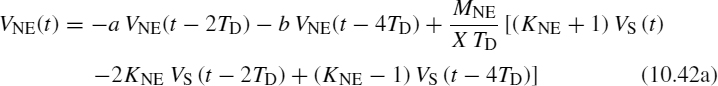

These equations can be solved recursively for the crosstalk voltages for an initially relaxed line, that is, VS(t) = VNE(t) = VFE(t) = 0 for t ≤ 0. The solutions are in terms of values of the source voltage at the present time, VS(t), and at various time delays prior to the present time: VS(t − TD), VS(t − 2TD), VS(t − 3TD), and VS(t − 4TD), as well as prior solutions at various time delays prior to the present time: VNE(t − 2TD), VNE(t − 4TD), VFE(t − 2TD), and VFE(t − 4TD).
10.2.1 Explicit Solution
Although the solution in (10.42) is exact, it requires knowledge of the solution at previous times that are multiples of the line one-way delay TD. Thus, a recursive solution is required. In order to obtain a solution that depends only on VS(t), we recall the time-shift or difference operator D, where
Using this time-shift operator along with (10.41) in (10.40) gives
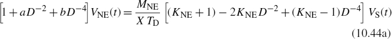

Multiplying the equations by powers of D gives the transfer functions in terms of the time-shift operator D as


These expressions can be inverted by carrying out the long division of the following basic problem:

where

Substituting the results of (10.46) into (10.45) gives the time-domain crosstalk voltages in terms of VS(t) delayed by multiples of the one-way line delay T as


where the constants are
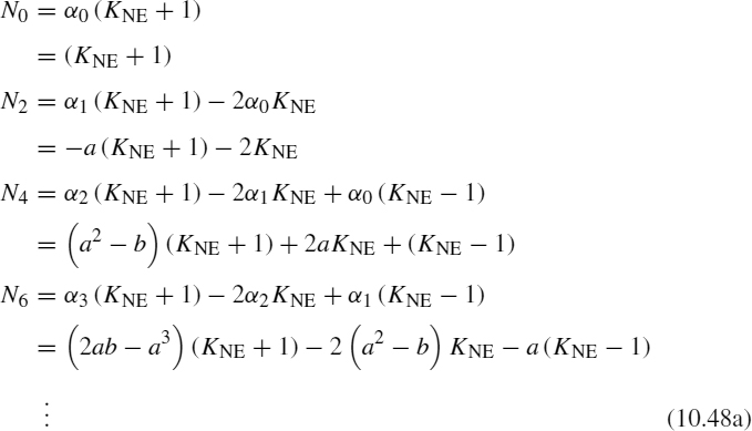

These final expressions give the explicit relationships for the crosstalk voltages as linear combinations of the source voltage delayed in time by various multiples of the line one-way delay TD.
Some additional interesting forms of these expressions can be obtained by grouping terms of (10.48) to yield


10.2.2 Weakly Coupled Lines
The above time-domain solutions are exact but somewhat complicated. In this section, we will assume that the lines are weakly coupled, that is, ![]() . In this case, P
. In this case, P ![]() 1 in Den, in which case the above results simplify considerably. The quantities in (10.39) factor, for P
1 in Den, in which case the above results simplify considerably. The quantities in (10.39) factor, for P ![]() 1, as
1, as


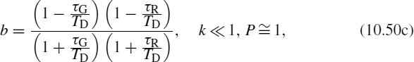
Assuming that the line is weakly coupled such that ![]() , the normalized time constants in (10.25) become
, the normalized time constants in (10.25) become


Now suppose that one of the ends of each line is matched; αSG = 1 or αLG = 1 and αSR = 1 or αLR = 1. In this case, the time constants in (10.25) become τG = TD and τR = TD. The quantities X, a, and b in (10.50) become X = 4, a = 0, and b = 0. The coefficients in (10.46b) are zero except for α0 = 1. The near-end and far-end crosstalk expressions in (10.49) simplify to

If the line is matched at the load end of the generator circuit, αLG = 1, or at the load end of the receptor circuit, αLR = 1, then KNE = 1 and (10.52) simplify to


There exist numerous electronic design handbooks and other publications that contain time-domain crosstalk prediction equations for three-conductor lines [5–11]. However, as pointed out previously, these invariably make the following assumptions:
- The line is weakly coupled.
- All ports are matched: αSG = αLG = αSR = αLR = 1.
- Both circuits have identical cross sections, for example, two identical wires at the same height above a ground plane. Hence, cG = cR and lG = lR.
These are very special restrictions that are generally not fulfilled in practical cases. For this special case where RS = RL = RNE = RFE = ZCG = ZCR = ZC, MNE and MFE in (10.29) reduce to

and the previously derived results in (10.53) reduce to


For a homogeneous medium, using (10.6) and (10.22), ![]() and the far-end crosstalk is (ideally) zero. For an inhomogeneous medium, the far-end crosstalk is not zero. These results are equivalent to results derived intuitively in [5–7]. Again, these results in (10.55) are restricted to lines that are (1) weakly coupled, (2) matched at all four ports, and (3) physically symmetric, that is, lG = lR and cG = cR. The total of these conditions is very ideal and is not found in practical applications.
and the far-end crosstalk is (ideally) zero. For an inhomogeneous medium, the far-end crosstalk is not zero. These results are equivalent to results derived intuitively in [5–7]. Again, these results in (10.55) are restricted to lines that are (1) weakly coupled, (2) matched at all four ports, and (3) physically symmetric, that is, lG = lR and cG = cR. The total of these conditions is very ideal and is not found in practical applications.
10.2.3 Inductive and Capacitive Coupling
In the frequency-domain solution, we observed that for a weakly coupled, electrically short line and for a sufficiently small frequency, the near-end and far-end crosstalk voltages reduce to (see (10.29))
The time-domain results can be obtained from these by substituting
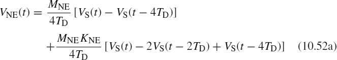
FIGURE 10.5 Illustration of near-end and far-end time-domain crosstalk predicted by the inductive-capacitive coupling model.
to give
For trapezoidal pulses representing, perhaps, digital clock or data signals, these results give crosstalk pulses occurring during the transitions of VS(t) with the levels of those pulses dependent on the slope or “slew rate” of VS(t) as illustrated in Figure 10.5. Substituting the definitions of MNE and MFE in (10.18) in terms of inductive and capacitive coupling contributions as given in (10.19) and (10.20) shows that this approximate time-domain crosstalk result can be computed from the equivalent circuit shown in Figure 10.6. Therefore, the time-domain crosstalk is the sum of an inductive coupling component and a capacitive coupling component.
The above time-domain result was obtained from the frequency-domain approximate result. In order for that frequency-domain result to be valid, the line must be electrically short at the highest significant sinusoidal frequency of excitation. Bounds on the spectrum of a periodic trapezoidal waveform representing a digital signal given in Chapter 1 are shown in Figure 10.7, where τr is the pulse rise time, and we assume that the rise time and fall time of the pulse are equal, τr = τf. Essentially, we require that the line be electrically short at the frequency components of the time-domain pulse waveform for frequencies up to some limit, fmax. We assume that the frequency components above this maximum frequency are decreasing in magnitude such that they do not substantially contribute to the pulse wave shape and hence incorrect processing of them by the time-domain model does not substantially introduce errors. For the trapezoidal waveform, the frequency components above the second break point, f = 1/π τr, are rolling off at −40 dB/decade. In Chapter 1, we obtained a criterion for the bandwidth of a trapezoidal, digital waveform as fmax = 3(1/π τr) ![]() 1/τr. Hence, we assume that the above approximate model is valid for frequency components below this. This gives a time-domain criterion for the validity of the approximate model given in (10.58) and Figure 10.6. Hence, we require that
1/τr. Hence, we assume that the above approximate model is valid for frequency components below this. This gives a time-domain criterion for the validity of the approximate model given in (10.58) and Figure 10.6. Hence, we require that
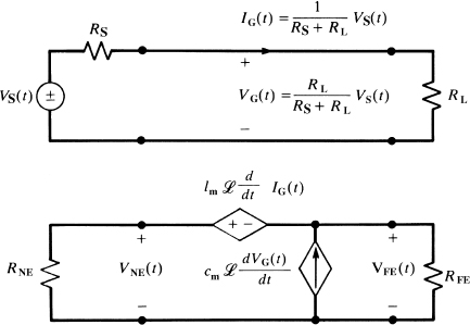
FIGURE 10.6 The time-domain inductive–capacitive coupling model.
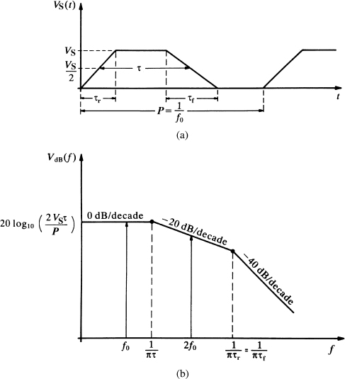
FIGURE 10.7 The frequency-domain representation of a periodic trapezoidal pulse train.

Rewriting this in terms of the line one-way delay, TD = ![]() /v, gives the criterion for validity of the approximate time-domain model as
/v, gives the criterion for validity of the approximate time-domain model as
10.2.4 Common-Impedance Coupling
The effect of the impedance of the reference conductor can be handled in an approximate manner at the lower frequencies of the pulse by simply adding the common-impedance coupling term to the inductive–capacitive contributions in (10.58):
where MNE and MFE are as given previously. The effect of common-impedance coupling is to add a scaled replica of VS(t) to the crosstalk resulting from inductive and capacitive coupling.
10.3 COMPUTED AND EXPERIMENTAL RESULTS
In this section, we will give some computed results comparing the predictions of the exact transmission-line model, the lumped-Pi model, and the inductive–capacitive coupling model developed in this chapter for three-conductor lines that were examined in the previous chapters. In all models, the conductors are considered to be lossless. For both structures, the SPICE subcircuit models were computed with the SPICEMTL.FOR, SPICELPI.FOR, and SPICELC.FOR computer programs de-scribed in Appendix A and combined into one SPICE program for ease of plotting of the results. The nodes at the input to the generator lines are designated as S1 (SPICE), S2 (lumped-Pi), and S3 (inductive–capacitive coupling model), whereas the nodes at the near end of the receptor circuit are designated as NE1 (SPICE), NE2 (lumped-Pi), and NE3 (inductive–capacitive coupling model). The termination impedances are all 50 Ω resistive, that is, RS = RL = RNE = RFE = 50 Ω.
10.3.1 A Three-Wire Ribbon Cable
The first configuration is a three-wire ribbon cable considered in previous chapters. See Figure 7.10. The wires are #28 gauge stranded (7 × 36) and are separated by 50 mils. One of the outer wires is the reference conductor, and the line is of total length 2 m. The per-unit-length parameters were computed in Chapter 5 with the RIBBON.FOR computer program described in Appendix A. Figure 10.8 compares the frequency-domain predictions for all three models over the frequency range of 1 kHz to 100 MHz. The line is one wavelength (ignoring the dielectric insulations) at 150 MHz, so we may consider it to be electrically short for frequencies below, say, 15 MHz. The lumped-Pi model gives good predictions below 10 MHz, whereas the inductive–capacitive coupling model gives good predictions below 1 MHz. This shows that the simple inductive–capacitive coupling model can give adequate predictions for a significant frequency range so long as its basic limitations are observed.
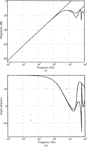
FIGURE 10.8 Illustration of the frequency response of the ribbon cable of Figure 7.10 via the SPICE model, one lumped-Pi section, and the inductive–capacitive coupling model: (a) magnitude and (b) phase.
Figure 10.9 shows the correlation between the three models for the time domain for the leading edge of the pulse. The source, VS(t), is a 1-MHz trapezoidal pulse train with 50% duty cycle. The trapezoidal pulses have 1 V magnitude with various rise times. The one-way time delay for the line (ignoring the dielectric insulations) is TD = ![]() /v = 6.67 ns, so we should not expect the inductive–capacitive coupling model to give adequate predictions for rise times less than 70 ns. Figure 10.9(a) shows the predictions for τr = 60 ns. The predictions of the lumped-Pi model compare well with those of the exact SPICE model. Figure 10.9(b) shows the predictions for τr = 120 ns, and Figure 10.9(c) shows the predictions for τr = 240 ns. Again, the predictions of the exact SPICE model and the lumped-Pi model correlate well. For the latter rise time of 240 ns, there is good agreement between the SPICE predictions and those of the inductive–capacitive coupling model for the peak crosstalk and τr = 36 TD.
/v = 6.67 ns, so we should not expect the inductive–capacitive coupling model to give adequate predictions for rise times less than 70 ns. Figure 10.9(a) shows the predictions for τr = 60 ns. The predictions of the lumped-Pi model compare well with those of the exact SPICE model. Figure 10.9(b) shows the predictions for τr = 120 ns, and Figure 10.9(c) shows the predictions for τr = 240 ns. Again, the predictions of the exact SPICE model and the lumped-Pi model correlate well. For the latter rise time of 240 ns, there is good agreement between the SPICE predictions and those of the inductive–capacitive coupling model for the peak crosstalk and τr = 36 TD.
Figure 10.10 shows oscilloscope photographs of the experimental results. For τr = 60 ns in Figure 10.10(a), the measured peak voltage is 80 mV compared to a predicted value of 80 mV. For τr = 120 ns in Figure 10.10(b), the measured peak voltage is 50 mV compared to a predicted value of 45 mV, and for τr = 240 ns in Figure 10.10(c), the measured peak is 26 mV compared to a predicted value of 23 mV. Observe in the measured results that, while the pulse is in its quiescent state of 1 V, the crosstalk does not go to zero as predicted by the lossless model but appears to asymptotically approach a value on the order of 2.5 mV, as shown in Figure 10.10(c). This is a result of common-impedance coupling. The per-unit-length dc resistance of one wire is obtained by dividing the dc resistance of one of the #36 gauge strands by 7 (the number of strands in parallel) to give a total resistance of the 2-m-long reference wire as r0![]() = 0.389 Ω. Substituting this into (10.34a) gives a common-impedance coupling level of 1.94 mV.
= 0.389 Ω. Substituting this into (10.34a) gives a common-impedance coupling level of 1.94 mV.
10.3.2 A Three-Conductor Printed Circuit Board
The next configuration is a three-conductor printed circuit board also considered previously. See Figure 7.13. The conductors (lands) are 15 mils in width and have thicknesses of 1.38 mils (1 ounce copper). They are on one side of a 47-mil-thick glass epoxy board and have edge-to-edge separations of 45 mils. One of the outer lands is the reference conductor, and the line is of total length 10 in. = 0.254 m. The per-unit-length parameters were computed in Chapter 5 with the PCB.FOR computer program described in Appendix A. Figure 10.11 compares the frequency-domain predictions for all three models over the frequency range of 10 kHz to 1 GHz. The line is one wavelength (assuming an effective relative permittivity as the average of the board and free space or ![]() at 700 MHz, so we may consider it to be electrically short for frequencies below, say, 70 MHz. The lumped-Pi model gives good predictions below 100 MHz, whereas the inductive–capacitive coupling model gives good predictions below 10 MHz. This again shows that the simple inductive–capacitive coupling model can give adequate predictions for a significant frequency range so long as its basic limitations are observed.
at 700 MHz, so we may consider it to be electrically short for frequencies below, say, 70 MHz. The lumped-Pi model gives good predictions below 100 MHz, whereas the inductive–capacitive coupling model gives good predictions below 10 MHz. This again shows that the simple inductive–capacitive coupling model can give adequate predictions for a significant frequency range so long as its basic limitations are observed.

FIGURE 10.9 Illustration of the time-domain response of the ribbon cable of Figure 7.10 via the SPICE model, one lumped-Pi section, and the inductive–capacitive coupling model for a rise/fall time of (a) 60 ns, (b) 120 ns, and (c) 240 ns.

FIGURE 10.10 The experimentally-determined time-domain response of the ribbon cable of Figure 7.10 for a rise/fall time of (a) 60 ns, (b) 120 ns, and (c) 240 ns.

FIGURE 10.11 Illustration of the frequency response of the printed circuit board of Figure 7.13 via the SPICE model, one lumped-Pi section and the inductive–capacitive coupling model: (a) magnitude, and (b) phase.
Figure 10.12 shows the correlation between the three models for the time domain. The source, VS(t), is again a 1 - V, 1 - MHz trapezoidal pulse train with various rise times. The one-way time delay for the line is (assuming an effective relative permittivity as the average of the board and free space or ![]() Td =
Td = ![]() /v = 1.43 ns, so we should not expect the inductive–capacitive coupling model to give adequate predictions for rise times less than 20 ns. Figure 10.12(a) shows the predictions for τr = 6.25 ns. The predictions of the lumped-Pi model compare well with those of the SPICE model. Figure 10.12(b) shows the predictions for τr = 20 ns, and Figure 10.12(c) shows the predictions for τr = 60 ns. Again the predictions of the SPICE model and the lumped-Pi model are virtually identical. For the latter rise time of 60 ns, the inductive–capacitive coupling model gives excellent prediction of the peak crosstalk magnitude and τr = 70 TD.
/v = 1.43 ns, so we should not expect the inductive–capacitive coupling model to give adequate predictions for rise times less than 20 ns. Figure 10.12(a) shows the predictions for τr = 6.25 ns. The predictions of the lumped-Pi model compare well with those of the SPICE model. Figure 10.12(b) shows the predictions for τr = 20 ns, and Figure 10.12(c) shows the predictions for τr = 60 ns. Again the predictions of the SPICE model and the lumped-Pi model are virtually identical. For the latter rise time of 60 ns, the inductive–capacitive coupling model gives excellent prediction of the peak crosstalk magnitude and τr = 70 TD.

FIGURE 10.12 Illustration of the time-domain response of the printed circuit board of Figure 7.13 via the SPICE model, one lumped-Pi section, and the inductive–capacitive coupling model for a rise/fall time of (a) 6.25 ns, (b) 20 ns, and (c) 60 ns.

FIGURE 10.13 The experimentally-determined time-domain response of the printed circuit board of Figure 7.13 for a rise/fall time of (a) 6.25 ns, (b) 20 ns, and (c) 60 ns.
Figure 10.13 shows oscilloscope photographs of the experimental results. For τr = 6.25 ns in Figure 10.13(a), the measured peak voltage is 94 mV compared to a predicted value of 95 mV. For τr = 20 ns in Figure 10.13(b), the measured peak voltage is 46 mV compared to a predicted value of 46 mV, and for τr = 60 ns in Figure 10.13(c), the measured peak is 17.5 mV compared to a predicted value of 15.8 mV. Observe in Figure 10.13(c) that, again while the pulse is in its quiescent state of 1 V, the crosstalk does not go to zero as predicted by the lossless model but appears to asymptotically approach a value on the order of 2.5 mV, as shown in Figure 10.13. This shows that common-impedance coupling can be significant even for short conductors. The total dc resistance of one land is r0![]() = 0.3279 Ω. Substituting this into (10.34a) gives a common-impedance coupling level of 1.64 mV.
= 0.3279 Ω. Substituting this into (10.34a) gives a common-impedance coupling level of 1.64 mV.
PROBLEMS
10.1 Show that the inverse of a 2 × 2 matrix
is

10.2 Solve, using Cramer's rule, Eqs. (10.16) to give the results in (10.17).
10.3 Derive the inductive–capacitaive coupling model results in (10.29).
10.4 Demonstrate the results in (10.31).
10.5 Derive the Laplace transform solution in (10.38).
10.6 Derive the time-domain recursive solution in (10.42).
10.7 Derive the explicit time-domain solution in (10.47).
10.8 Demonstrate the relations in (10.50) and (10.51).
10.9 Obtain the simplified relations in (10.52)–(10.54).
10.10 Consider a problem consisting of three identical, bare wires wherein one of the wires serves as the reference conductor. The wires are #28 gauge stranded wires (7 × 36) (radius 7.5 mils) and are arranged on the corners of an equilateral triangle so that the separations between each wire are 1 cm. The terminations are RS = 50 Ω, RL = 1k Ω, RNE = 300 Ω, and RFE = 100 Ω. If the total line length is 2 m, compute the near-end and far-end frequency-domain crosstalk (magnitude and angle) using (6.17) from 1 kHz to 100 MHz. Determine the coupling coefficient, the near-end and far-end crosstalk coefficients ![]() and
and ![]() , and the frequency where the line is 0.1 λ. long. Compare your results with those of the SPICE model, SPICEMTL.FOR, to show that (10.17) is correct.
, and the frequency where the line is 0.1 λ. long. Compare your results with those of the SPICE model, SPICEMTL.FOR, to show that (10.17) is correct.
10.11 For the structure of Problem 10.10, repeat the crosstalk calculations using the low-frequency, inductive–capacitive coupling model in (10.29). Verify your results using the SPICE model generated by SPICELC.FOR.
10.12 For the structure of Problem 10.10, assume that VS(t) is a 1-MHz periodic train of trapezoidal pulses with equal rise/fall times of 100 ns and a level of 1 V. Compute the time-domain near-end and far-end crosstalk using the iterative solution given in (10.42). Repeat these calculations for rise/fall times of 50 ns and 10 ns. Verify your results using the SPICE model generated by SPICEMTL.FOR.
10.13 Repeat Problem 10.12 using the low-frequency, inductive–capacitive coupling approximation given in (10.58). Verify your results using the SPICE model generated by SPICELC.FOR.
10.14 Determine the common-impedance coupling waveform for Problem 10.12.
10.15 Reproduce the results of Figures 10.8 and 10.9 using the SPICE models generated by SPICEMTL.FOR, SPICELPI.FOR, and SPICELC.FOR.
10.16 Reproduce the results of Figures 10.11 and 10.12 using the SPICE models generated by SPICEMTL.FOR, SPICELPI.FOR, and SPICELC.FOR.
10.17 Explain why you would expect to obtain the inductive–capacitive coupling models in the limit as the frequency goes to zero. [Hint: The current of the generator circuit produces a magnetic flux that links the receptor circuit. Now use Faraday's law to determine the induced voltage in the receptor circuit and assume weak coupling between the lines. Similarly, the voltage of the generator circuit produces an electric field some of which terminates on the receptor conductor that induces a charge on that conductor.]
REFERENCES
[1] L. Young, Parallel Coupled Lines and Directional Couplers, Artech House, Dedham, MA., 1972.
[2] V.K. Tripathi, Asymmetric coupled transmission lines in an inhomogeneous medium, IEEE Transactions on Microwave Theory and Techniques, 23 (9), 731–739, 1975.
[3] R. Speciale, Even- and odd-mode waves for nonsymmetrical coupled lines in nonhomogeneous media, IEEE Transactions on Microwave Theory and Techniques, 23 (11), 897–908, 1975.
[4] J.C. Isaacs, Jr. and N.A. Strakhov, Crosstalk in uniformly coupled lossy transmission lines, The Bell System Technical Journal, 52 (1), 101–115, 1973.
[5] W.R. Blood, Jr., MECL System Design Handbook, 4th edition, Motorola Semiconductor Products Inc., 1988.
[6] A. Feller, H.R. Kaupp, and J.J. Digiacoma, Crosstalk and reflections in high-speed digital systems, Proceedings, Fall Joint Computer Conference, 511–525, 1965.
[7] J.A. DeFalco, Predicting crosstalk in digital systems, Computer Design, 69–75, June, 1973.
[8] D.B. Jarvis, The effects of interconnections on high-speed logic circuits, IEEE Transactions on Electronic Computers, 12 (5), 476–487, 1963.
[9] I. Catt, Crosstalk (noise) in digital systems, IEEE Transactions on Electronic Computers, 16 (6), 743–763, 1967.
[10] A.J. Rainal, Transmission properties of various styles of printed wiring boards, The Bell System Technical Journal, 58 (5), 995–1025, 1979.
[11] H. You and M. Soma, Crosstalk analysis of interconnection lines and packages in highspeed integrated circuits, IEEE Transactions on Circuits and Systems, 37 (8), 1019–1026, 1990.