
5
Basic and Advanced SoC Interfaces
In this chapter, we will define an SoC interface for a given function. Then, we will look at the different memory interfaces for on-chip and off-chip memories, their topologies and architectural features, and the criteria for choosing a given interface (or a combination of many). We will cover the fundamentals of the processor caches and the memory management unit (MMU) while focusing on the Cortex-A9 implementation. Finally, we will explore the main data storage interfaces.
In this chapter, we’re going to cover the following main topics:
- Interface definition by function
- Processor cache fundamentals
- Processor MMU overview
- Memory and storage interface topology
Interface definition by function
As a generic definition, an interface in an SoC is a hardware block that acts as a proxy through which transactions are converted from one domain into another. The domain itself depends on the type of interface in question and what transformation it performs. We can distinguish many functions in an SoC topology, some of which are as follows:
- Type 1: A peripheral that performs a dedicated task in the hardware within the same chip, such as an interrupt controller, a system timer, or a central direct memory access (DMA) engine.
- Type 2: A peripheral that performs a dedicated task in the hardware in another chip external to the SoC, such as a temperature sensor, a radio-frequency integrated circuit (RFIC), or an analog-to-digital converter (ADC).
- Type 3: A peripheral that acts as an input/output (I/O) device such as a general-purpose input/output (GPIO) device or a display controller.
- Type 4: A peripheral that performs a low-speed communication task, such as a universal asynchronous receiver/transmitter (UART).
- Type 5: A peripheral that performs a high-speed communication task, such as an Ethernet controller, a Bluetooth controller, or a wireless local area network (WLAN) controller.
- Type 6: A bridge from one network-on-chip (NoC) to another or interconnect within the same SoC, such as an AXI to APB bridge, a high-speed NoC to a low-speed and low-power peripheral interconnect, or the processing subsystem (PS) to the programmable logic (PL) bridge within the Zynq-7000 SoC, as introduced in Chapter 1.
- Type 7: A bridge between the SoC chip and another high-speed integrated circuit (IC) residing within the same electronics board, such as a Peripheral Component Interface Express (PCIe).
- Type 8: A bridge between the SoC chip and another low-speed IC residing within the same electronics board such as a serial peripheral interface (SPI) or an inter-integrated circuit (I2C) bus controller.
- Type 9: A plug-and-play controller such as a universal serial bus (USB) controller.
- Type 10: A form of local storage within the SoC chip, such as read-only memory (ROM), static random Access memory (SRAM), or one-time programmable (OTP) arrays.
- Type 11: A form of external storage to the SoC chip, such as Dual Data Rate Synchronous Dynamic Random Access Memory (DDR SDRAM), Low-Power Dual Data Rate Synchronous Dynamic Random Access Memory (LPDDR SDRAM), or flash memory.
- Type 12: A hardware accelerator implemented within the SoC chip, such as a security accelerator engine or a mathematical computation engine.
The common factor between all these functions is that they all connect to the SoC internal NoC or interconnect from one side, and either connect to the chip’s internal resources or external I/O pads propagating their reach off-chip. The following diagram depicts the interface by function concept:
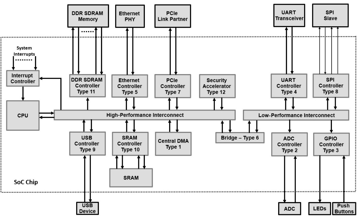
Figure 5.1 – SoC interfaces and their type classification
SoC interface characteristics
As mentioned previously, the interface bridges two domains, and as such, it is required to implement all the services needed to make this bridging possible. In the transfer function fulfilled in this bridging, usually, the clocking is different, either increasing or decreasing, as well as being asynchronous. This bridging can be unidirectional or bidirectional with some or no dependencies between the two data transfer directions. Often, the processor needs to set the operating mode of the function, check the status of operations, and intervene when necessary to either take on follow-up actions or reset the functionality of the device in case of errors. These are provided as a set of configuration and control registers that software programs use when powering up the SoC or when a mode change in how the function operates is desired. The data transfer process, as covered in Chapter 3, Basic and Advanced On-Chip Busses and Interconnects, can either be performed by the processor itself from the function’s temporary storage buffers or automatically triggered when data is available and then transferred via an integrated DMA engine within the function itself. Usually, domain crossing is done through FIFOs, which also act as temporary storage while certain conditions are met to transfer the data to its destination. The function also uses a set of registers to log operational information of interest to the processor, gather runtime and functional statistics to analyze the behavior, and estimate the function’s performance. The function also provides notifications to the processor via a set of interrupts or a single interrupt acting as a proxy for many lower-level interrupts. There is usually an array of registers for logging all the necessary information that the processor can read to decide on further actions and reset operating conditions, when necessary, in case of operational errors, for example. The function has a reset control mechanism that implements all the reset functionalities required by the function itself, such as the system reset, the interfaces reset, the external device controller reset, and so on, as defined by the function microarchitecture. When we look at all these operational details that a function acting as an interface requires, except for Type 6, which acts as an internal SoC bridge from one NoC to another or interconnect, we notice that there is a common set of services that an interface implements (some or all) to fulfill its transfer function.
In summary, these interface services are as follows:
- The SoC internal data plane bus interface, which implements the SoC data plane bus protocol, such as an AXI, ACE, or OCP
- The SoC internal control plane bus interface, which implements the SoC bus protocol, such as an APB, an AHB Lite, or an AXI Stream
- The SoC interconnect clock domain to the function’s hardware internal clock domain crossing in the write or transmit direction (as seen from the processor’s perspective)
- The function hardware’s internal clock domain to the SoC interconnect clock domain crossing in the read or receive direction (as seen from the processor’s perspective)
- The transmit/write FIFO or buffer within the function hardware block
- The receive/read FIFO or buffer within the function hardware block
- The DMA write channel within the function hardware block
- The DMA read channel within the function hardware block
- The interface’s main transfer function that’s implemented within the function’s hardware
- The function’s configuration, control, and status registers file
- The function’s interrupt mechanism implementation with all the registers required to enable, mask, and trigger the function’s single or multi-interrupts mechanism
- The function and interfacing logic system reset control
The following diagram depicts the function services concept in an SoC interface:
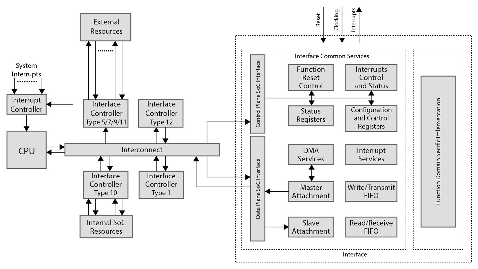
Figure 5.2 – Common interface services
The aforementioned function services are not necessarily present in all SoC interfaces as their range of complexity is wide, and the interface tends to implement the services required to perform the desired transfer functions. When implementing our custom interface in the advanced section of this book, we will start the microarchitecture design of the interface controller from a known set of services and design the interface using the services that provide the desired interface transfer functions.
SoC interface quantitative considerations
When designing, or sometimes even when configuring, an SoC interface provided by a third-party vendor as a configurable IP that can be tailored to a user SoC application, other quantitative considerations will dictate whether certain services are needed, such as using an integrated DMA engine or just relying on the SoC central DMA engine when it has one, using a FIFO and which size to implement, and which frequency to clock the core function at, for example. In these cases, knowledge of the SoC system’s performance requirements is a necessity for defining these elements. The SoC’s overall architecture should have defined these performance parameters or at least provided the system requirements from which to derive them.
When looking at the overall SoC interface performance, the main data bus and the type of runtime data transfer supported by the interface, such as the burst size, the issuing capabilities (IC) of the bus interfaces, the frequency at which it is running, and any interface internal buffering capabilities, help in computing the overall internal SoC side performance of the interface. The bus protocol transfer metrics are provided by the bus standards specification. The ARM AMBA bus collection and the OCP bus protocol were introduced in Chapter 3, Basic and Advanced On-Chip Busses and Interconnects, where some of the parameters affecting their performance were covered.
The interface controller’s domain-specific performance figures are usually set and predefined by the protocol (if any) to which the interface is performing the transfer function – for example, 1 Gbps for a Gigabit Ethernet controller and 3.4 Mbps in the high-speed mode of an SPI controller.
Given that the bus protocol supports data transfers via the interface, the domain protocol-specific metrics for which the controller is interfacing, and the interface internal function buffering capabilities, we can usually compute the interface performance figures and make decisions regarding the interface function configuration or choose a particular SoC implementation.
Processor cache fundamentals
Most processors used in modern SoCs include a Level 1 Instruction Cache (L1I$) and a Level 1 Data Cache (L1D$). Some processors also include an L2 Shared Cache (L2S$), which is used for both processor instructions and data per processor core, or like in the ARM Cortex-A9 cluster where it is used for both instructions and data, and shared between all the cores. In some modern processors in a multi-core processor cluster, there is also an L3 Common Cache (L3C$) between all the processors in the cluster. The caches are used to shorten the latency of the processor’s access to instructions and data while executing the software as they are implemented using SRAMs and running at the processor clock frequency, which is relatively higher than the remaining logic surrounding the processor in the SoC. Also, external memory access latency is usually many orders of magnitude higher than the access time to the internal SRAM implementing the cache within the processor core. This reduces the bus accesses performed by the processor to frequently running code and accessed data of the software, therefore reducing both the bottlenecks on the SoC interconnect and the shared memory hosting the software image and thus optimizing the overall SoC power consumption. The power is reduced by shortening the data movement on the SoC busses and avoiding unnecessary access to external memory. Access to external memory uses external pads which consume more power in comparison to accessing internal SRAM or ROM memory. In this section, we will focus on the processor cache organization in general and look at the ARMv7 architecture that’s used in the Cortex-A9 processor, which is implemented within the PS of the Zynq-7000 SoC earlier in this book. The following diagram depicts the hierarchical view of the processor caches in the Cortex-A9 processor cluster:
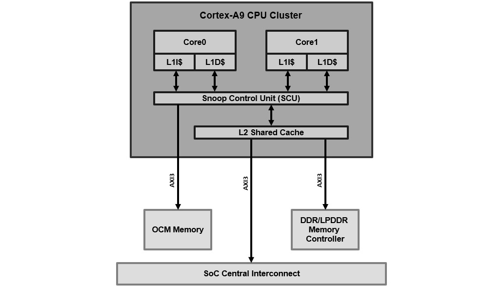
Figure 5.3 – Cortex-A9 processor cache hierarchy
The Snoop Control Unit (SCU) is responsible for maintaining the cache coherency between the different caches and the external memory by implementing a cache coherency protocol called MESI, which was introduced in Chapter 3, Basic and Advanced On-Chip Busses and Interconnects.
Processor cache organization
When the processor needs access to data or instructions held in the external memory, the address of that data or instruction is looked up in the first-level cache – that is, the L1D$ for data or the L1I$ for the instructions. If there is a hit – that is, this address is held in the L1D$ or L1I$ – then the data or the instruction is returned from the cache. If there is a miss, then the next-level cache – in this case, the L2S$ – is looked up and the data or instruction is returned from the L2S$ in the case of a cache hit; otherwise, the request is forwarded to the physical memory.
The memory content is loaded into the cache in cache line units. For the Cortex-A9, a cache line is 32 bytes in size. Cache memory sizes are limited to avoid increasing the SoC cost and slowing down the processor clock speed. Due to this, managing the use of the caches and placement of the code and data in the memory of the SoC software is a key element in the SoC system performance metric, which we will study in Part 3 of this book. When observing the software execution on an SoC processor, two aspects are noted:
- The code’s locality, which reflects the instructions and data that are executed at a specific period. These tend to be close to each other (in terms of addresses – that is, the physical location in memory, such as when executing loops).
- The other aspect is that software execution tends to reuse the same addresses over time (such as when calling the same function many times), which is the temporal locality aspect of the software's code and data.
Using caches in an SoC processor has the potential to improve the system software’s execution performance by reducing the external memory access latency and decreasing the energy cost of the software execution. However, this will introduce some degree of non-determinism that the application should be aware of to define a correctly behaving system. Caches are smaller in size than the external memory and are usually not big enough to hold all of the software application and its associated data. So, when code is fetched for the first time from external memory, its execution time acts as though the cache isn’t present; it is only on subsequent access to the same code and data while still in the cache that the system will benefit from the reduced latency and increased performance. This induced non-uniform latency can be a concern for hard real-time systems that require a deterministic response time, regardless of the use of a cache. In these systems, deadlines should be estimated and bound as if the cache is non-existent by placing the code and data in non-cacheable regions or tightly coupled memories (TCM) for processor architectures that have one. The Cortex-A9 doesn’t have this, but it does have an on-chip memory (OCM) provision in the PS that can be used as a non-cacheable memory region to hold critical data and instructions for software that is sensitive to determinism, for example.
Cache topology and terminology
The following diagram shows how the ARM cache is organized and the associated terminology necessary to understand the operating behavior of the caching mechanism in an ARMv7-A architecture:
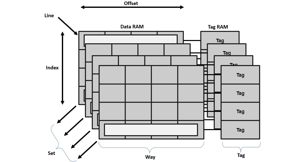
Figure 5.4 – ARMv7-A cache organization
The following table provides a summary of the terms used in the ARMv7 architecture cache’s organization:
|
Term |
Definition |
|
Cache |
A storage location for the processor’s data and instructions. |
|
Data RAM |
This stores the address content of either the data or the instructions. |
|
Tag RAM |
This stores the address information. |
|
Line |
This is the smallest data or instructions unit from the system memory that the cache operates on. |
|
Tag |
This is part of the cache line address in the system memory that’s stored in the cache. |
|
Index |
This is part of the cache line address in the system memory and can be found in the cache. |
|
Offset |
This is part of the cache line address in the system memory and via which a specific word can be found in the cache line. |
|
Way |
This is an equal-size logical grouping of multiple cache lines. |
|
Set |
This is a logical grouping of cache ways looked up simultaneously for a specific cache line. They have the same index values. |
Table 5.1 – Cache organization terminology
Directly mapped cache
Since the cache is smaller in size than the main SoC memory, a mapping between the cache and the main memory needs to be implemented to define where the specific memory region of a cache line size can be stored in the cache. We distinguish caches that are directly mapped and others that are set-associative. In a directly mapped cache, a memory address can only be held in a single cache location, as shown in the following diagram:
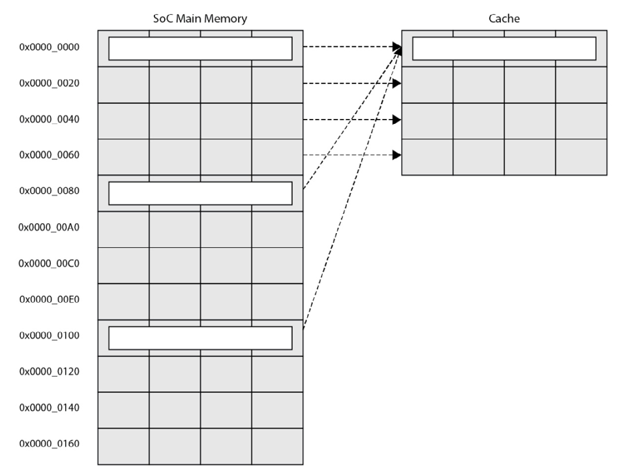
Figure 5.5 – Directly mapped cache
In the preceding diagram, the index bits (address[5:4]) are used to read the tag values stored in the cache. If there is a match and the address line is valid, then there is a hit. The line (address[3:2]) and the offset (address[1:0]) are used to locate the relevant data value within the cache line. The value of the cache line address to store is the remaining 26 bits (address[31:6]), which will be looked up in the tag memory to find out whether the memory location is cached when the processor needs to access it. The following diagram illustrates the cache line address utilization for a directly mapped cache:
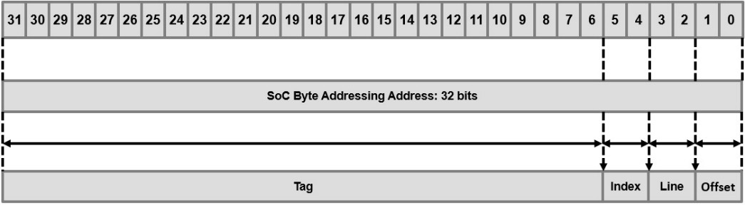
Figure 5.6 – Directly mapped cache line address format
Set-associative cache
As shown in the preceding diagram, memory addresses will be competing for the same cache line location in the cache and causing cache trashing and increasing traffic between the cache and the system memory, which results in higher power consumption and lower system performance. To circumvent this, we need to have multiple ways to host the memory address in the cache. This can be achieved with set-associativity. A set-associative cache increases the number of locations where a memory address can be stored in the cache, thus providing more chances to keep the cache line replacement low. The following diagram illustrates the set-associative cache approach:

Figure 5.7 – A two-way set-associative cache organization
In this cache organization, the capacity of the cache is split into many ways. A memory location can then be mapped to a way and not to a specific line like in the directly mapped cache introduced in the previous section. The line is still identified using the index field of the address in each way of the set. Consequently, cache lines with the same index values belong to the same set. For a cache hit, we must look at every tag in the set. In the ARM cache implementations of L1I$ and L1D$, two-way and four-way set-associative caches are usually used. In the L2S$, and because the L2S$ is usually bigger by at least an order of magnitude than the L1 caches, the number of ways is higher, and usually 8- or 16-way set-associative caches are common.
For more information regarding the ARMv7 architecture cache’s implementation, please read Section 8 of Caches of the ARM Cortex-A Series Programmer’s Guide at https://developer.arm.com/documentation/den0013/latest.
ARM Cortex-A9 Technical Reference Manual also contains some useful architectural-specific details on caches for the Cortex-A9: https://developer.arm.com/documentation/ddi0388/latest.
Processor MMU fundamentals
Another modern processor architectural feature, specifically for the Cortex-A series CPUs, is the MMU. It allows the software tasks running on the processor to use virtual memory addressing as it performs the address translation back to the physical memory when access is needed. It also implements access management in the address spaces from the processor to the physical memory to prevent and allow read, write, and execute access from tasks to the translated regions of the physical address space. The MMU allows software to be written without any knowledge of the physical address space mapping or whatever else may be running on the processor. It can also make mappings between a continuous virtual address space to a fragmented physical address space. The firmware running on the processor is responsible for setting up the MMU, as well as the address translation tables, to make the desired correspondence between the virtual view of the SoC address map seen by the software to the actual physical address map of the SoC. The following diagram shows what the MMU can perform in this respect:
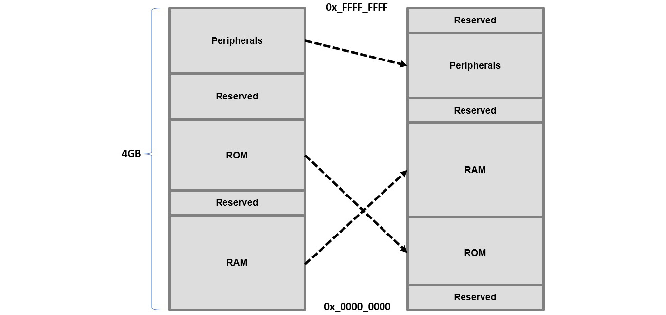
Figure 5.8 – MMU address translation operation
The virtual address space is on the left side of the preceding diagram, whereas the physical address map is on the right side.
The MMU can be disabled (it is at boot time by default) and in this case, the virtual address map is mapped directly to the physical address map with all types of access enabled. The MMU performs the address translation by using page tables (called translation tables in ARM architecture terminology) that are created by software in the SoC’s physical memory.
The addresses generated by a processor are virtual addresses that are then translated into physical addresses as they cross the MMU when enabled. If we think of the address space as a set of contiguous regions with different sizes, these regions can be mapped anywhere in the address map using several of the most significant bits. Effectively, this is the basis of the translation job performed by the MMU. Each region should also have some attributes that define the permissions that are checked as the translation is performed. If these permissions are not allowed or the region is not mapped, then an exception fault is generated by the MMU. Translation table walking refers to the process of reading the translation tables from memory by the MMU hardware during the translation process.
The translation look-aside buffer (TLB) is used as a caching mechanism by the MMU hardware for the translation tables. So, rather than fetching from memory at every translation operation, it keeps the recently used translation tables in this buffer (or cache), making translating the address from virtual memory to physical as fast as possible. When the translation table is accessed from the TLB, this is called a TLB hit.
The contiguous memory regions in the mapping job of the MMU are called translation pages. The smaller a page is, the better it is to efficiently use the memory space when allocation is done for different software processes that shouldn’t share memory, for example. However, this introduces a higher number of translation tables and therefore, potentially inefficient use of the TLB. For example, a software process requires 15 KB of memory. Here, assigning 4 x 4 KB pages is fine since only 1 KB is wasted, but for a process that requires 128 KB, if we assign a page that’s 1 MB, then a lot of memory space is wasted. However, with larger page sizes, TLB entries are more likely to maximize the hit rate, thus avoiding external memory for the translation table walking, which decreases performance. 16 MB supersections can be used for larger memory region allocations to processes where a detailed and restrictive mapping is required. To come up with an efficient translation scheme for a given SoC software, specifically when not using an OS, you may need to experiment with a few translation schemes using different page sizes to find the best compromise.
The MMU address translation process in a Cortex-A9 processor can involve many steps and uses multiple translation tables in its implementation.
The process of the address translation and how many steps are included in it for the ARM Cortex-A9 processor are described in detail in Section 9 of the ARM Cortex-A Series Programmer’s Guide at https://developer.arm.com/documentation/den0013/latest.
The ARM Cortex-A9 Technical Reference Manual also contains some useful architectural-specific details on the MMU and its hardware implementation for the Cortex-A9: https://developer.arm.com/documentation/ddi0388/latest.
Memory and storage interface topology
In this section, we will focus on the memory and storage controllers available in the PS of the Zynq-7000 SoC since we will need to configure them for Part 2 of this book. We will examine their microarchitectural features, their main configuration parameters, and how they affect the system performance aspects. In this section, we will cover the following Zynq-7000 SoC interfaces:
- DDR memory controller
- Static memory controller
- On-chip memory controller
Let’s get started.
DDR memory controller
The DDR memory controller that’s integrated within the PS of the Zynq-7000 SoC can be used to interface to DDR2, DDR3, DDR3L, and LPDDR2 type SDRAM memories. It is a multiport controller from the SoC side, and its bandwidth can be simultaneously shared between its four ports for both read and write transactions. It has four AXI3 internal ports that are full duplex. A port is connected directly to the L2 cache of the Cortex-A9, allowing it to service the processor cores and making the DDR memory cache coherent via the ACP of the Cortex-A9 with any external master to the PS. Another port is shared between all the internal masters within the PS via the central interconnect, and the two remaining ports are dedicated to the SoC programmable logic through two AXI3 64-bit full duplex interfaces. The DDR controller is formed of three main microarchitectural blocks:
- DDRI, which interfaces to the SoC interconnect via the 64-bit four AXI3 interfaces. It provides stage-1 arbitration access and buffers the command and data using the implemented internal FIFOs.
- DDRC, which is the core of the controller with the necessary logic to perform the per-port read/write stage-2 arbitration and the transaction scheduling in an optimal way (stage-3). This maximizes the bandwidth utilization of the attached external DDR DRAM memory while also minimizing latency for urgent transactions.
- DDRP, which is the PHY interface that translates the DDRC selected commands into DDR DRAM-specific transaction signals that obey its timing sequencing and requirements.
The following diagram depicts the DDR memory controller system’s connectivity within the Zynq-7000 SoC:

Figure 5.9 – DDR memory controller-centric view of the Zynq-7000 SoC
DDR memory controller features and configuration parameters
The DDR memory controller has the following SoC interface characteristics:
- The AXI interface has the following features:
- Four ports, each with a 64-bit full duplex data interface with 32-bit addressing capabilities
- All ports support both AXI INCR and WRAP bursts
- A multi-port arbitration protocol that maximizes DRAM bandwidth utilization
- Arbitration logic that can be bypassed for low-latency transactions
- High acceptance capability per port for both read and write commands
- Out-of-order read completion for read transactions with different master IDs and an AXI ID width of 9 for all ports
- 1 to 16 beats burst length, with a burst size of 1, 2, 4, or 8 bytes per beat
- Programmable secure regions on 64 MB boundaries using a system-level register
- Exclusive accesses are only supported for two different master IDs and only per port, not across ports
- The DDRC controller has the following features:
- DDR DRAM memory data throughput and low latency-aware transaction scheduling algorithm (a three-stage arbitration and command selection mechanism, as shown in Figure 5.12)
- A transaction reordering engine to optimize the DDR DRAM access bandwidth for both sequential and random access
- Read and write address dependency detection for data access coherency
- The DDRP PHY controller has the following features:
- Supported DDR I/Os: 1.2V LPDDR2, 1.8V DDR2, 1.5V DDR3, and 1.35V DDR3L
- 16-bit and 32-bit physical memory data width supported
- Software controller self-refresh mode with automatic exit when there are commands to execute
- Programmable idle periods timing for the automatic DDR power down entry and exit
- Automatic calibration for the data read strobe
Port S0 of the DDR memory controller is dedicated to the Cortex-A9 L2 cache interface and the ACP. On the DDRI side, this port is usually configured for low latency access.
Port S1 serves the other PS masters via the SoC central interconnect.
Ports S2 and S3 serve the programmable logic side of the SoC via a switching interconnect. On the DDR memory controller side, these ports are usually configured for high throughput.
The DDR memory controller has 1 GB of address space allocated to it in the 4 GB SoC address map. The following table shows the possible physical devices supported and their arrangements:
|
Device |
Component Configuration |
Number of Components |
Component Density (GB) |
Total Width |
Total Density |
|
DDR3/DDR3L |
x16 |
2 |
4 |
32 |
1 GB |
|
DDR2 |
x8 |
4 |
2 |
32 |
1 GB |
|
LPDDR2 |
x32 |
1 |
2 |
32 |
256 MB |
|
LPDDR2 |
x16 |
2 |
4 |
32 |
1 GB |
|
LPDDR2 |
x16 |
1 |
2 |
16 |
256 MB |
Table 5.2 – Zynq-7000 SoC DDR memory controller example DRAM memory organization
Quality of Service (QoS) is implemented in the DDR memory controller’s DDRC using a combination of the round-robin arbitration algorithm among the four port queues and an aging mechanism assigned to each queue via a software-controlled register. There is also an input signal representing an urgent request on a port that resets the aging counter, making it the highest priority queue. The arbitration algorithm also uses page matching to decide which command queue to service. The page, which is the DDR memory page, is open at the time of the arbitration. The following diagram illustrates the arbitration algorithm (stage-1) that’s used by the DDRC to arbitrate between the ports:
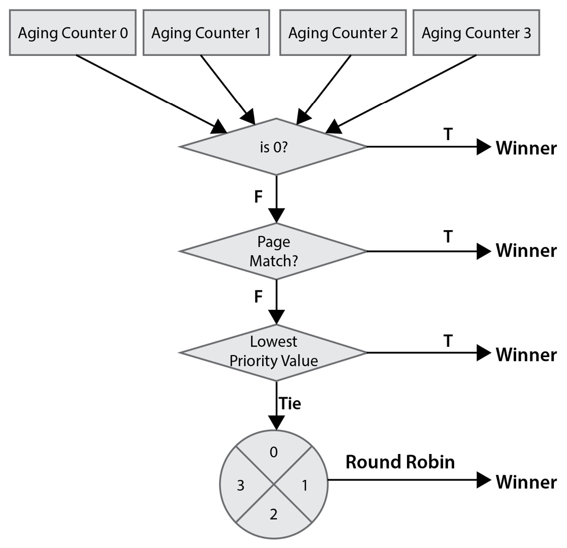
Figure 5.10 – DDR memory controller ports arbitration algorithm
Within the DDRC core, there is another stage of arbitration (stage-2) between the read and the write command queues. The following diagram illustrates this stage of arbitration in the Zynq-7000 SoC DDR memory controller:
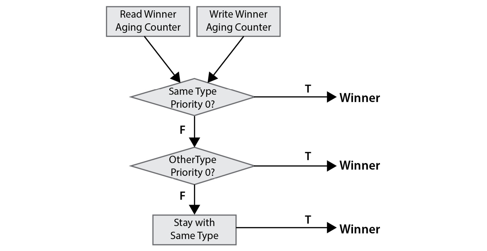
Figure 5.11 – DDR memory controller read and write queues arbitration algorithm
In this second stage of arbitration within the DDRC, the aging counter is checked. Then, an older one is selected. If the next command from it has a priority of 0 and is like the previous one (already selected in the previous arbitration cycle), then it wins the arbitration. For example, assuming that in the previous cycle, the command was a read transaction, the queue that is the oldest is the read queue, and the read command has a priority of 0, then it is the winner of this arbitration cycle, and the next read transaction is elected to be executed next. If it is not the same type of command with a priority of 0, and another type of transaction with a priority of 0 is next, then that one will win. If there is no transaction with a priority of 0 in the queues, then the winning transaction is from the same queue as the previous transaction.
It is important to understand these arbitration schemes to figure out which stream of commands will be serviced next and how such a scheme may affect the overall performance of the system, especially in applications where the overall software processing architecture relies on a pipelined model. This will help in choosing which QoS attributes to assign to a port that’s used for a specific data stream.
The DDRC also has an optional feature that is called high priority read (HPR). Here, the read data queue is split into two separate queues – one for high-priority transactions and another for low-priority transactions. Every port of the DDR memory controller can be qualified as a high or low priority according to the application needs and the nature of the data streams it services – for example, assigning a high-priority read to port 0, which is servicing the CPU. This feature needs to be enabled to be used. The following diagram provides an overview of all the arbitration stages a command goes through before being executed by the DDRC and forwarded to the DDR DRAM memory device:

Figure 5.12 – DDR memory controller commands full arbitration stages
The DDRC also has a write combining feature, which can be enabled to exploit merging many write commands to the same address from different commands.
There are many other operational details related to the DDR memory controller, such as the clocking, the reset, the startup sequence, and the controller calibration, which we will cover in Part 2 of this book when we put an SoC project together that uses the DDR SDRAM as its system’s main memory. We will also practically assess the effect certain parameters have on the system’s overall performance by putting together a benchmarking software example that can measure the effects on system performance for the given parameter settings. For details on these, you are invited to examine Chapter 10 of the Zynq-7000 SoC Technical Reference Manual at https://docs.xilinx.com/v/u/en-US/ug585-Zynq-7000-TRM.
Static memory controller
The static memory controller (SMC) can be used to interface to a NAND flash, SRAM, or NOR flash memory. It has an AXI3 slave interface for the data transfers between the SoC and the memory media attached to it, and an APB slave interface to configure the registers of the SMC and read status when necessary.
SMC features and configuration parameters
The SMC has an interrupt (IRQ ID# 50) that is connected to the Cortex-A9 generic interrupt controller (GIC). The SMC can operate either as a NAND flash interface and address up to 1 GB of flash memory, or as a parallel SRAM/NOR flash interface and address up to 32 MB per chip select (CS) pin. The SMC has two CS pins, so it can address two dual 32 MB regions of attached SRAM and/or NOR flash memories. The following diagram provides a microarchitectural representation of the SMC:

Figure 5.13 – SMC microarchitecture diagram
The SMC NOR or NAND flash memory can be used as a booting device for the Cortex-A9 CPU. For details on clocking and reset options, the external connectivity, the APB registers file, and other operational information, you are invited to explore Chapter 11 of The Zynq-7000 SoC Technical Reference Manual at https://docs.xilinx.com/v/u/en-US/ug585-Zynq-7000-TRM.
On-chip memory controller
The OCM controller is an interface within the PS that has an internal SRAM of 256 KB and a BootROM of 128 KB. The OCM controller presents two AXI3 64-bit interfaces to the SoC masters, one connected to the Cortex-A9 CPU and the other shared between all the other SoC masters (from the PS and PL) via a memory interconnect. The following diagram shows the system view of the OCM controller in the PS block:

Figure 5.14 – On-chip memory controller-centric view of the Zynq-7000 SoC
OMC features and configuration parameters
The OCM SRAM is divided into 64 x 4 KB pages for which the security attributes (access rights and modes) can be assigned on a per-page basis. The OCM also has a configuration APB slave port and an interrupt signal with ID#35. The CPU/ACP interface to the OCM is on a low latency path but still has a minimum of 23 cycles for read latency when the CPU is running at 667 MHz. Arbitration between the AXI read and write channels is done round-robin from the OCM interconnect, and the arbitration between the CPU/ACP port and the OCM interconnect ports is fixed with the highest priority to the CPU/ACP one. The OCM, due to its lowest access latency from the CPU perspective compared to the DDR DRAM, can be used to host the critical parts of the SoC software, such as the TLB tables, the interrupt service routines, the exceptions code, and any functions that are real-time in nature and greatly affect the system’s response time. The OCM is also good for hosting the DMA engine descriptors, as well as any other parts of the code or data that are bound by real-time constraints for it to be accessed. Further details on OCM clocking, its address mapping, and the address relocation options will be covered in Part 2 of this book when we configure the OCM for critical code and data section hosting. Information on the APB registers file, as well as other operational information, is available in Chapter 29 of the Zynq-7000 SoC Technical Reference Manual at https://docs.xilinx.com/v/u/en-US/ug585-Zynq-7000-TRM.
Summary
This chapter started by providing an architectural and functional overview of what SoC interfaces are while classifying them by functionality. Then, we listed the main services needed to perform such an interfacing function. After that, we provided a summary of the main features that globally affect the SoC’s system performance that need to be considered when designing an SoC interface of a specific type. Then, we looked at the fundamentals of the processor caches while focusing on the ARMv7 architecture implementation in the Cortex-A9 CPU and covered their associated terminology and topologies. After that, we looked at the cache organizations, the possible mappings, and how caches improve the SoC system performance. We also introduced the processor MMU and its role in virtual to physical address translation, physical address space management, and SoC security implementation. Next, we provided a detailed introduction to the DDR memory controller as being one of the fundamental SoC interfaces where the software application and the system’s main data are stored. Here, we looked at the multi-port nature of the Zynq-7000 SoC DDR memory controller and how transactions from the different ports are arbitrated for access to the memory media at the different stages of their processing by the DDR memory controller. We also introduced the static memory controller and the different types of memory and flash devices that can be connected to the SoC through it, as well as its main architectural features and performance metrics. Finally, we introduced the OCM controller as a major complementary storage interface for the DDR memory controller for hosting the critical parts of the SoC software and as the default BootROM of the PS.
This was the closing chapter of Part 1 of this book, where we mainly focused on the fundamentals and the basic knowledge you need to start designing and implementing an SoC using Xilinx FPGAs. The next chapter will be the opening chapter of Part 2 of this book, where we will look at the SoC architecture design and development process before moving on to putting the SoC together and building, verifying, and integrating all its critical components.
Questions
Answer the following questions to test your knowledge of this chapter:
- What is an SoC interface? How can we classify one?
- How does classifying the SoC interfaces help with designing a custom SoC interface?
- Build a table where you list the various interface types we can distinguish, and provide the main services for each.
- How could we compute the depth of a write/transmit FIFO for an SoC interface if we are given the read IC of the AXI3 port of the interface as 16, the speed of the SoC interconnect as 400 MHz, the type of the interface as 5, and the external domain as having a transmission speed of 250 Mbps?
- How is a processor cache organized? Define all the parameters that are used in the Cortex-A9 cache topology.
- What is a cache tag? How is its length computed?
- What is a set-associative cache? What are the main advantages of using a set-associative cache versus using a direct mapped cache?
- How many ways do we usually find in an L1 ARMv7 implemented cache? What about L2 caches?
- What is a processor MMU?
- What is a processor virtual address?
- How does a virtual address get translated into a physical address?
- How many ports does the DDR memory controller of the Zynq-7000 SoC have? Why is this topology used?
- How many transaction command arbitration stages are there in the DDR memory controller of the Zynq-7000 SoC? Explain the principle of each and how the possible choices can affect the system’s performance.
- What are the main features of the Zynq-7000 SoC static memory controller?
- What types of memory are used in the OCM controller? Explain the system uses of each.
- Why is the OCM controller’s CPU/ACP port given the highest arbitration priority for its AXI3 read sides among all the other ports?