
9
SoC Design Hardware and Software Integration
In this chapter, you will complete the steps involved in an SoC-based FPGA design. You will download the FPGA binary configuration file describing the ETS SoC to the target hardware board if you have one to hand. If no demo board capable of hosting the ETS SoC hardware design is available, you will still be able to use an emulator platform based on a system model provided by Xilinx to perform some of the SoC system design integration tasks. The virtual system will allow you to boot the SoC CPU, load it with the executable file to simply run it, or proceed to debug the application software on the virtual target as if it was the real hardware hosting it. This chapter is mainly hands-on in that you will be guided through every step of the SoC hardware and software integration and testing phases using the Vitis IDE and the Xilinx emulation platform. This is the closing chapter of Part 2, which has covered most of the SoC system design and development topics introduced in Part 1, but with an emphasis on their practical aspects. We have based this chapter on a complex design involving many of the topics we have studied thus far and tried to illustrate a few of them at a time, so the principles will be mastered, and you are prepared to tackle more complex topics in both the hardware and software design techniques of modern SoCs.
We have gone from the concept of designing an Electronic Trading System (ETS) SoC to building its actual components. We have specified the design and the system requirements, built the hardware, and exported the design from the hardware design environment to the software design environment. Within the Vitis IDE, we configured the BSP and the drivers and generated the test software for both ETS SoC CPUs, and in this chapter, we will put all these parts together to run the software on the ETS SoC hardware. We will be using a real electronics board or a virtual platform emulating the SoC in its operating environment.
In this chapter, we’re going to cover the following main topics:
- Connecting to an FPGA SoC board and configuring the device
- The emulation platform for running the embedded software
- Using the emulation platform to debug the SoC test software
- Embedded software profiling using the Vitis IDE
Technical requirements
The GitHub repo for this title can be found here: https://github.com/PacktPublishing/Architecting-and-Building-High-Speed-SoCs.
Code in Action videos for this chapter: http://bit.ly/3fOdrEc.
Connecting to an FPGA SoC board and configuring the FPGA
Once the application software for the ETS SoC design has been compiled using the Vitis IDE and its executable image has been generated, we can proceed to the next phase: connecting to the FPGA board from the Vitis IDE to download the FPGA SoC bitstream. This phase requires that a JTAG cable is connected from the host machine to the demo board. The JTAG cable is usually plugged into the host machine’s USB port. If you are using the UbuntuVM environment, as suggested in this book, the drivers for the Xilinx JTAG cable aren’t installed, and you will need to install them separately using the Vivado Lab solutions available at https://www.xilinx.com/support/download.html.
This will install the JTAG cable drivers and the necessary device packages that will allow this version of the Vivado tools to connect to the hardware board. Alternatively, you will need to use Vivado and Vitis IDEs on a native OS version that is officially supported by the Xilinx tools. This will then install the JTAG cable drivers as part of the Vitis installation process, and therefore you can connect directly from the Vitis IDE to the board. In the remaining parts of this chapter, we will focus on the Xilinx emulator platform to maximize the usefulness of these practical parts to everyone.
Another aspect of the hardware and software integration in the Xilinx SoC design flow is the automatic loading of the executable file that was mapped by the linker script to the FPGA BRAMs. In the ETS SoC design, all the sections of the MicroBlaze PP executable file were mapped to the LMB BRAM by the linker script. Given that the BRAMs are part of the PL side of the FPGA, they are configured from a hardware design perspective via the FPGA bitstream like any other hardware macro of the FPGA, but the Vitis tools also initialize these BRAMs’ content with the executable file sections. This step is automatically run whenever a Build All command is executed in Vitis using a bootloop executable file to initialize the MicroBlaze LMB BRAM with. This can be changed to the test application executable we built for the MicroBlaze PP in Chapter 7, FPGA SoC Hardware Design and Verification Flow, as can be seen in Step 4.
To download the FPGA bitstream from the Vitis IDE, follow these steps:
- From the Vitis IDE main menu, click Xilinx | Program Device:
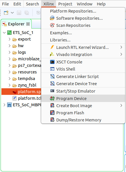
Figure 9.1 – Launching the Vitis IDE Program Device wizard
- In the Program Device window shown in the following screenshot, set the bitstream file path, the BMM/MMI File location, and the executable file to load into MicroBlaze. Leave all the other settings as the defaults and click Program. This will launch the board’s JTAG discovery and then program the Zynq-7000 FPGA device with the bitstream initializing the LMB BRAM with the MicroBlaze PP bootloop executable.
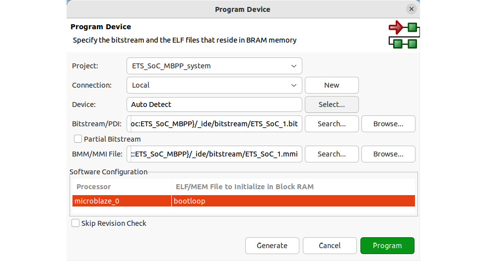
Figure 9.2 – Setting the Program Device options
- The MicroBlaze PP executable file can be changed to the one built in Chapter 8, FPGA SoC Software Design Flow, for the ETS SoC project. You can modify it by browsing to its location and selecting it as the executable file for the microblaze_0 processor instance in the Program Device wizard.
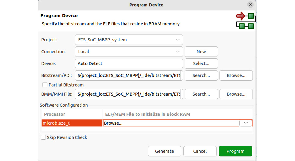
Figure 9.3 – Changing the executable file for the MicroBlaze PP
- When you select Browse…, press Enter on your keyboard and the executable file associated with the microblaze_0 hardware instance will be automatically found, which you can then select by clicking Open.
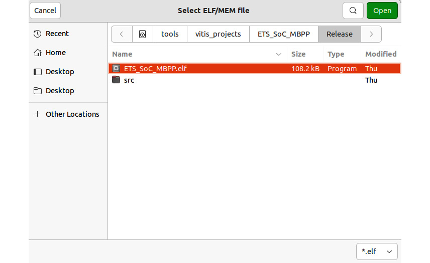
Figure 9.4 – Selecting an application executable file for the MicroBlaze PP
- The ETS_SoC_MBPP.elf file is now mapped to the LMB BRAM in the FPGA bitstream. To update the bitstream, you can now click Generate, which will call the updatemem Vitis utility that updates the FPGA bitstream with the MicroBlaze PP executable Executable and Linkable (ELF) file.

Figure 9.5 – Updating the FPGA bitstream with the MicroBlaze PP executable file
The emulation platform for running the embedded software
Xilinx provides an emulation platform for the Zynq-7000 SoC, the MicroBlaze embedded processor, and the Zynq UltraScale+ MPSoC. It is based on the Quick Emulator (QEMU), which is a Linux-based emulation platform that allows us to build a virtual system including the SoC with all its internal hardware component modules, its external interfaces, and all the surrounding electronics board integrated circuits. It is therefore a suitable environment for software development and prototyping. These ports emulate board-level systems with many peripheral models included. QEMU is already integrated within the Vitis IDE and can be directly called as if we were targeting a demo board.
Information
For the list of features and supported devices by the Xilinx QEMU ports, check Chapter 2 of the Xilinx Quick Emulator User Guide at https://docs.xilinx.com/v/u/2020.1-English/ug1169-xilinx-qemu.
In the ETS SoC project, we will only be able to target a single CPU at a time: either the Cortex-A9 PS subsystem or the MicroBlaze PL subsystem. However, this is enough to get started and interact with the software part of the SoC design using the associated Vitis IDE tools for introducing debugging techniques. We will target the Cortex-A9 processor in this chapter. It is worth mentioning that Xilinx provides a way of performing QEMU and user logic co-simulation via remote ports, which uses a SystemC/TLM2.0 interface, which requires the PL side of the design to be built in SystemC, Verilog, or VHDL. This method could be a way of integrating custom logic built in the PL part of the Zynq-7000 with QEMU, and therefore have the MicroBlaze PP simulating in RTL and the Cortex-A9 of the PS in QEMU; however, this is outside the scope of this book.
Using QEMU in the Vitis IDE with the ETS SoC project
As already mentioned, QEMU is integrated into the Vitis IDE, which means that there is already a virtual platform that can be used as a prototyping environment for the test software we have built for the Cortex-A9 processor. This virtual environment presents itself as if it was the real hardware on which the executable file is running, and therefore can be used natively with the Cortex-A9 executable we built in Chapter 8, FPGA SoC Software Design Flow. To use QEMU as a demo platform in the Vitis IDE, just follow these steps:
- To launch QEMU, go to Xilinx in the Vitis IDE main menu and then click Start/Stop Emulator:
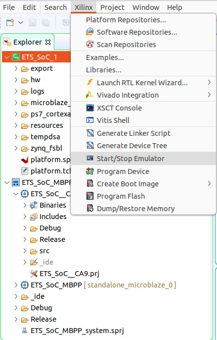
Figure 9.6 – Launching QEMU in the Vitis IDE
- The following wizard will open, showing the project and its associated configuration. Click Start to launch QEMU.

Figure 9.7 – Launch menu of QEMU in the Vitis IDE
QEMU will then start its console window in the Vitis IDE.

Figure 9.8 – QEMU console in the Vitis IDE
Figure 9.9 – Running the software on QEMU in the Vitis IDE
- The following WARNING window will open as we have already launched a QEMU session, but without any software loaded on it. Click OK to relaunch QEMU, this time with the software executable of the Cortex-A9 core0 loaded on the platform and automatically started.

Figure 9.10 – QEMU warning in the Vitis IDE
The QEMU console will act as a terminal for the embedded software and captures its output.

Figure 9.11 – Results of running the software on QEMU in the Vitis IDE
- We can observe from the results that some tests have passed and two have failed, while the last test appears to be still running. The logical action to take is to get some debugging going so we get some answers to why these didn’t return PASSED. Stop the session by going to the Vitis IDE main window and clicking Xilinx | Start/Stop Emulator, as shown in Figure 9.6.
- The following window will open. Click Stop.
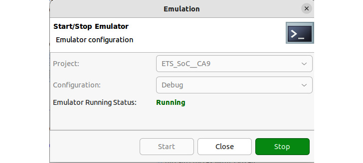
Figure 9.12 – Stopping QEMU in the Vitis IDE
The following message will then appear, confirming that QEMU has been stopped:
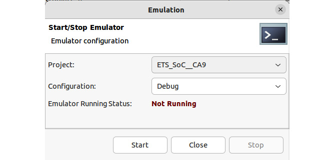
Figure 9.13 – QEMU session status in the Vitis IDE
Using the emulation platform for debugging the SoC test software
QEMU can be used as a virtual target to debug the software we built in Chapter 8, FPGA SoC Software Design Flow, for the ETS SoC project. Readers with experience of using Eclipse-based SDK debugging of embedded software running on a hardware target board will find it similar to using QEMU as a target debug environment in the Vitis IDE. To connect QEMU as a debug target, let’s go through the next steps:
- We need to configure or examine the Debug Configuration… option to use. Right-click on the Debug build under ETS_SoC_CA9 and click Debug | Debug Configuration….
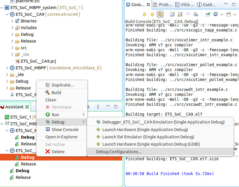
Figure 9.14 – Accessing the Debug Configuration... menu in the Vitis IDE
- This will open the following window. Select Debugger_ETS_SoC_CA9-Emulation, tick the Emulation entry, and make sure that all the settings match the following screenshot:

Figure 9.15 – Specifying the debug configuration in the Vitis IDE
- Select the Application tab and make sure that the Download option specifies the executable linked to the Cortex-A9 core 0 processor (ps7_cortexa9_0) as shown. Make sure that Stop at ‘main’ is ticked. Click Debug.

Figure 9.16 – Specifying the executable to debug in the Vitis IDE
- This will then connect the debugger to QEMU, download the executable file, and release the Cortex-A9 to run until it reaches the entry point of main(). The Vitis IDE switches its view to the Eclipse-based SDK debugger.

Figure 9.17 – Specifying the executable to debug in the Vitis IDE
- Set some breakpoints and then click on Resume. This will run the software until it reaches the breakpoint, where it stops.

Figure 9.18 – Resuming software execution on QEMU in the Vitis IDE debugger
- To stop the execution of the debugger, you can click on Suspend.
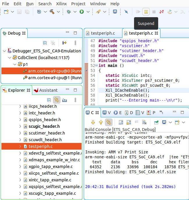
Figure 9.19 – Suspending software execution on QEMU in the Vitis IDE debugger
- Execution will stop and show where the software execution is at. This is in the ps7_scuwdt_0() test, which didn’t finish executing during the free running session earlier. The Watchdog Timer test isn’t hanging, it is running fine and waiting for a timeout to occur to complete the test.

Figure 9.20 – Examining the Timeout value of the Watchdog Timer model in the Vitis IDE debugger
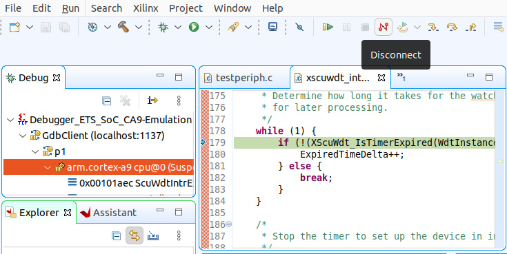
Figure 9.21 – Disconnecting the debugger from QEMU in the Vitis IDE debugger
Embedded software profiling using the Vitis IDE
To use the Vitis IDE for software profiling, we need to connect to a target hardware board. To launch the software profiling, follow the next steps:
- Click on the arrow next to the play button in the Vitis IDE main menu. Click Run Configurations….

Figure 9.22 – Launching the Profiling menu in the Vitis IDE
- The Run Configuration menu will open. Select the Debugger_ETS_SoC_CA9-Performance under SPM Analysis as shown. This window will allow you to configure the profiling launch options.
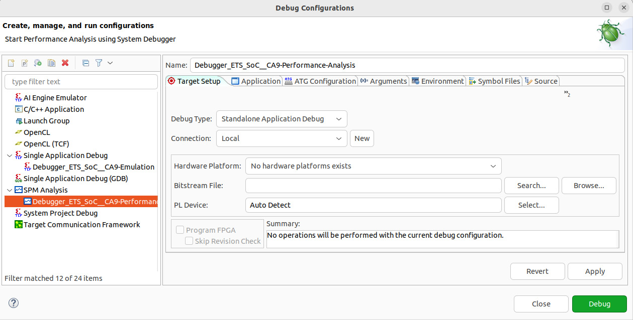
Figure 9.23 – Configuring the Profiling Launch Options in the Vitis IDE
- Click Debug to connect the debugger to the target hardware board for profiling.
You can now profile the application software running on the Cortex-A9 processor on the target hardware board. You can examine the call graph and the histograms and study the system’s runtime behavior to highlight areas for performance improvement.
Summary
In this chapter, we looked at the remaining final steps and utilities to complete the FPGA-based SoC system design. We have seen that using an FPGA SoC isn’t so different from an SoC development targeting an ASIC technology. This is the result of the tight integration of the hardware and the software flows facilitated by the Vitis IDE, which takes over from the Vivado IDE using the XSA hardware information. The Vitis tools then inherit all the information related to the hardware platform, such as the memory map, the list of IPs, and the FPGA configuration file to boot the FPGA with, from the Vitis IDE. We have seen how easy it is to proceed to download the FPGA binary configuration file describing the ETS SoC design to the target hardware board from the Vitis IDE. Software development can start using QEMU as a virtual development platform. This emulator is easily accessible from within the Vitis IDE. The virtual system allowed us to boot the SoC CPU. We could also load it with the executable file and fully run it on the emulation target. We have also been able to perform software debugging on QEMU using an Eclipse-based SDK-like IDE debugger within the Vitis IDE. In this chapter, we have completed the last phase of the system co-design by performing the hardware and software integration. We have also executed some system-level testing using the template software test examples.
This chapter closes Part 2 of this book, which has covered most of the SoC system design and development topics in practical, easy-to-follow steps. We have gone from the concept of designing an ETS SoC to building its actual components. We specified the design and the system requirements, built the hardware, exported the design from the hardware design environment to the software design environment, configured the BSP and the drivers, and generated the test software for both ETS SoC CPUs. We have also put all these parts together to run the software on the ETS SoC hardware using a real electronics board or a virtual platform emulating the SoC. We are now ready to tackle more complex embedded system design topics, such as platforms design for an embedded Linux or a Real-Time Operating System (RTOS) including the system-level security aspects and data coherency between the PS and the PL accelerators over the Cortex-A9 Acceleration Coherency Port. These and other FPGA SoC-based applications in different industry verticals will be discussed in Part 3 of this book.
In the next chapter, we will explore some advanced and challenging SoC design topics, which will allow us to efficiently connect hardware accelerators to the Cortex-A9 processor using coherent data-sharing mechanisms. We will also learn how to analyze the performance of these IPC mechanisms.
Questions
Answer the following questions to test your knowledge of this chapter:
- Is it possible to program the FPGA using the Vitis IDE? How would you do that?
- If the MicroBlaze executable is hosted in the LMB BRAM, which utility is used to integrate it into the FPGA bitstream file?
- Why do we need to initialize the LMB BRAM with the MicroBlaze executable prior to configuring the FPGA SoC?
- Describe the steps used in the Vitis IDE to update the FPGA SoC bitstream using a new MicroBlaze executable ELF file.
- What is QEMU?
- What are the characteristics of the Xilinx QEMU? Which processors from Xilinx SoCs does it support?
- Describe the steps to launch QEMU from the Vitis IDE.
- How different is debugging the Cortex-A9 software using the Xilinx port of QEMU in comparison to using a real hardware board?
- Describe the steps needed to debug the Cortex-A9 software on the QEMU emulator.
- How can we profile the Cortex-A9 software?