13
Video, Image, and DSP Processing Principles in an FPGA and SoCs
In this chapter, you will learn about some of the advanced applications implemented in modern FPGAs and SoCs and what makes these devices such powerful compute engines for these types of processing- and bandwidth-demanding applications. You will gain clarity on how the parallel processing required by Digital Signal Processing (DSP) applications in general can be easily implemented in the FPGA logic and how these parallel compute engines can be interfaced to wide memories and the powerful CPUs available in the SoCs. This chapter is purely informative and introduces high-level architectural details that may inspire you in designing and building these kinds of applications.
In this chapter, we’re going to cover the following main topics:
- DSP techniques using FPGAs
- DSP in an SoC and HW acceleration mechanisms
- Video and image processing implementation in FPGA devices and SoCs
DSP techniques using FPGAs
Performing DSP in an FPGA or an SoC-based FPGA, such as the Zynq-7000 SoC or the UltraScale+ MPSoC, is no different than performing it in an Application-Specific Integrated Circuit (ASIC) specifically built for such operations. There are many advantages to performing DSP operations in an FPGA technology in comparison to using an ASIC and these are mostly due to the flexibility, extensibility, and scaling advantages of using an FPGA-based DSP solution. Classically, FPGAs were chosen to implement DSP computation units for many industries, telecommunication being one of the dominant ones. Wireless communication standards were still evolving and the time to market was, and is still, an important business objective, making using a flexible solution, such as FPGA-based DSP, an attractive option. In these applications, most of the time, the FPGA device was a companion chip to a powerful processor. The architecture of these solutions evolved around reconfigurability as software running on the processor could be changed and upgraded even post the product deployment, and so are the FPGA DSP compute engines changeable and upgradeable. These types of architectures are still in deployment, but some users sometimes have preferences for using a processor architecture that is not based on ARM; however, these users are in the minority nowadays. The following diagram helps in visualizing the simple concept of a dual-chip solution to solve most of the DSP-intensive design challenges:

Figure 13.1 – Conceptual diagram of an electronic system using a dual-chip solution for DSP
Most applications requiring a processor and a companion FPGA to perform hardware acceleration and specifically intensive DSP computations will find an FPGA-based SoC attractive for performing their DSP operations. As we already know, these types of devices combine both a powerful processor and a rich logic elements resource. This combination and integration of both the processor subsystem and the FPGA logic for the DSP implementation within the same device has many advantages, such as the following:
- Reduction of the Bill of Materials (BOM) requirements
- Optimization of the overall solution’s power consumption and power design
- Enhancement of the performance in terms of throughput between the two domains
- Reduction of the electronics board size and thus the overall product volume
Zynq-7000 SoC FPGA Cortex-A9 processor cluster DSP capabilities
FPGA-based SoCs, such as the Zynq-7000 SoC, offer a powerful DSP operations-capable engine within the Cortex-A9 cluster called NEON Media Processing Engine (MPE). NEON designates an ARM Intellectual Property (IP) used for the Advanced Single Instruction Multiple Data (SIMD) functionality of ARMv7 and ARMv8 Cortex-A and Cortex-R processors. SIMD is a generic term referring to performing in parallel multiple operations on similar datasets when the dataset is of a smaller size than the processor width. A simple example is to perform four parallel addition operations (ADD4) on 8-bit datasets using a 32-bit processor. In this example, the single instruction is the ADD4 operation, and the multiple datasets would be the two 32-bit vectors holding each of the four 8-bit datasets. The following figure illustrates the basic SIMD concept on a 32-bit processor:

Figure 13.2 – SIMD example for a four-way 8-bit unsigned integer ADD operation
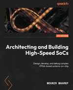
In the ARMv7 architecture specification, the Advanced SIMD extension was added to the ARMv7-A and ARMv7-R profiles. The SIMD concept is further expanded by the addition of new instructions, which take as operands 64-bit vectors (doubleword) and 128-bit vectors (quadword). These Advanced SIMD instructions operate on 64-bit and 128-bit registers and their implementation by ARM is called NEON. The following figure shows the NEON ADD16 operation:
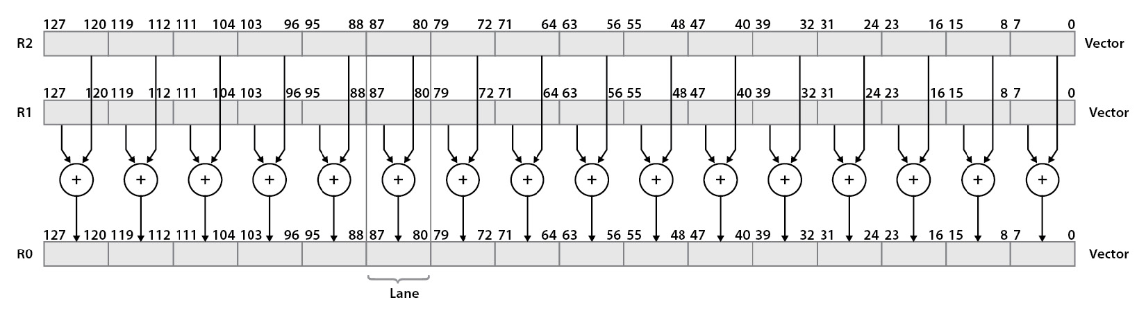
Figure 13.3 – NEON example for a 16-way 8-bit unsigned integer ADD operation
The preceding simple example is provided to visualize the principles of the NEON implementation in the ARM architecture. This helps in understanding the basis of performing the fundamental mathematical processing using a 32-bit processor but operating on wider vectors of datasets in parallel. These provide a huge performance improvement in comparison to sequentially performing the same operation on a pair of datasets at a time; however, the software code and the data representation should be optimized or vectorized to map well to NEON use.
Information
The following article provides more information on NEON architecture, implemented operations, and the supported data types: https://developer.arm.com/documentation/dht0002/a/Introducing-NEON/What-is-SIMD-/ARM-SIMD-instructions.
Zynq-7000 SoC FPGA logic resources and DSP improvement
Exploiting parallelism in the SIMD concept is going to improve the throughput when there is a chance to perform the same operation on multiple datasets. However, there is no possibility to pipeline many of these operations and avoid storing back to memory and loading from it. Data movements from/to the system memory are required to perform successive operations when using a processor, even with a SIMD engine, whereas by using an FPGA-based SoC, this kind of multiple SIMD operations pipelining is easy to implement. The following figure illustrates the extra capability of pipelining DSP operations and avoiding storing back to memory and reloading datasets to perform the next series of operations. This is also possible as we can extend the computation units to any number required to implement the desired parallel and pipelined DSP architecture.
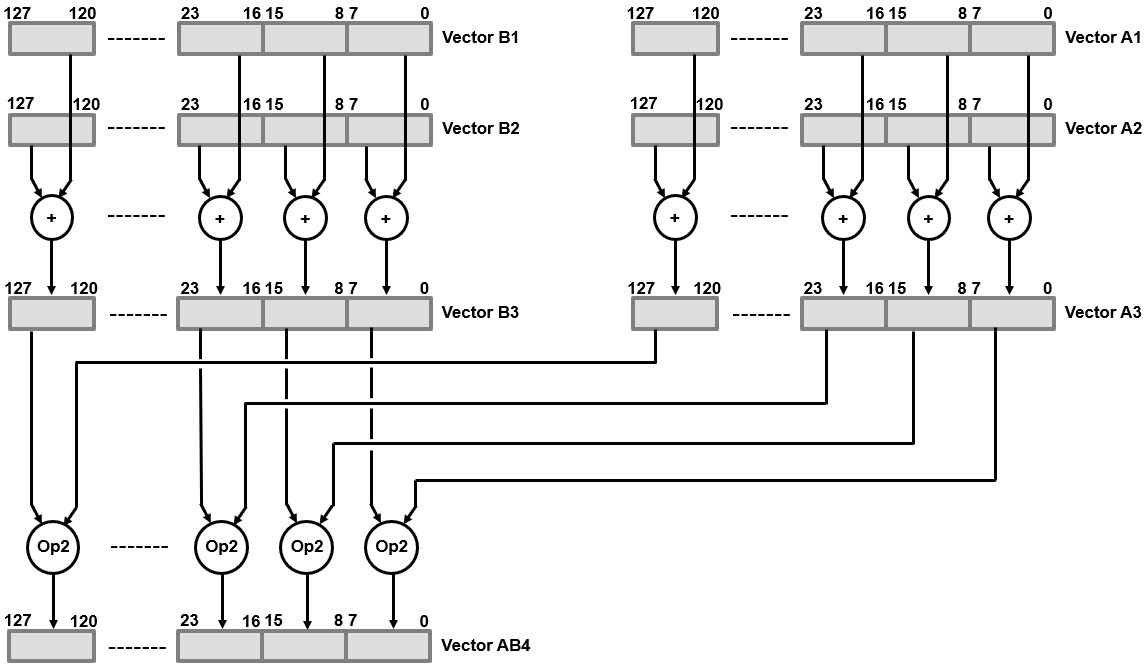
Figure 13.4 – DSP computation using the FPGA parallelism and pipelining capabilities
The FPGA logic elements, DSP slices, and distributed registers provide an extensive pool of resources to implement any mathematical function in a cost-effective way that is hard to beat using a classical processor, even with its attached coprocessing units, such as SIMD engines. When using a Zynq-7000 SoC FPGA, the computation algorithm can be mapped in such a way that sequential, control, and house-keeping operations are run on the Cortex-A9, whereas intensive mathematical operations are performed by the FPGA logic. The FPGA logic can implement wide and deep DSP engines that can operate on a large bank of datasets.
Zynq-7000 SoC FPGA DSP slices
The Zynq-7000 SoC FPGAs include many DSP slices, depending on the device size and density. The DSP slice architecture looks as in the following figure:
Figure 13.5 – Zynq-7000 SoC FPGA DSP slice architecture
The DSP slice contains a 25 x 18-bit two’s complement multiplier and 48-bit accumulator. When not needed, the multiplier can be bypassed, resulting in two 48-bit vector inputs to the SIMD engine. The SIMD arithmetic unit can operate on a dual 24-bit or quad 12-bit dataset per vector and is able to perform addition, subtraction, and accumulator operations. It is also capable of performing logic operations.
Information
Details of the Zynq-7000 SoC DSP slices are available at https://docs.xilinx.com/v/u/en-US/ug479_7Series_DSP48E1.
DSP in an SoC and hardware acceleration mechanisms
DSP computation extensibility using the FPGA logic resources is just a special case of the hardware acceleration techniques covered in the previous chapters of this book. It is therefore a matter of architecture design to split and coordinate what will be running on the Cortex-A9 embedded software and what computation will be shifted to the FPGA logic resources implementing the DSP engines.
Accelerating DSP computation using the FPGA logic in FPGA-based SoCs
In an FPGA-based SoC such as the Zynq-7000 SoC, DSP computation can be implemented using the FPGA logic and DSP resources. The SoC architecture should define how the shared data to operate on should be moved around the SoC, how the results shall be shared with the Cortex-A9, and any external entity that the Zynq-7000 SoC FPGA interfaces with. Obviously, it is also important to design an Inter-Processor Communication (IPC) mechanism that is optimal and avoids any system bottlenecks. The following diagram provides a system overview of the DSP computation extensibility and the possible data paths and communication paths in the Zynq-7000 SoC FPGA:

Figure 13.6 – Zynq-7000 SoC FPGA DSP computation integration
As shown by the preceding figure, and like the already-introduced hardware acceleration integration techniques in the previous chapters of this book, the DSP computation engines can be integrated into the SoC design using the same approach. The interfacing can be implemented over the High-Performance (HP) 64-bit AXI slave ports for high-throughput data accesses from the DSP engine masters to the SoC domain and external memory. Low- and medium-throughput operations from the DSP engines can make use of the General-Purpose (GP) 32-bit AXI slaves. From the Processing Subsystem (PS) masters, the GP 32-bit AXI masters provide a gateway to access the DSP engine address space. For a cache-coherent data exchange and sharing between the DSP computation engines and the Cortex-A9 processor, the 64-bit AXI slave ACP port can be used.
Video and image processing implementation in FPGA devices and SoCs
Video processing, specifically real-time video processing, requires intensive DSP computation. In the last decade, we started observing the proliferation of these applications in embedded systems, which possess a limited amount of computation, storage, and power resources. The emergence of IoT and distributed systems is adding to the abundance of computationally demanding devices with these limited resources. Many architectures are also evolving to solve this dilemma and balance the processing requirements and the limited resources in these devices. Several applications, such as object detection, video surveillance, machine vision, and security, are using FPGA-based SoCs where the PS implements the device security, communication, and control, whereas DSP-intensive operations are offloaded to the FPGA logic to implement the computationally intensive algorithms. This approach is helping to minimize the time to market and the overall solution cost.
Xilinx AXI Video DMA engine
Xilinx provides the AXI Video Direct Memory Access (VDMA) IP core, which is a Direct Memory Access (DMA) engine adapted for video applications. It can perform video data read and write transfer operations from an AXI mapped address space to an AXI4-Stream destination. It can also execute transfers in the opposite direction. This IP integrates features that are specific to the video systems. These include genlock and frame sync for fully synchronized frame DMA operations as well as two-dimensional DMA transfers.
Both the scatter/gather or register direct mode operations are provided by the AXI VDMA IP for data transfers controlled by the central processor. The AXI VDMA has an AXI4-Lite slave interface for the IP initialization, status, and control registers access. The AXI VDMA core can handle data conversion and padding from the common 24-bit format in video applications to the 32-bit generic AXI interface. The AXI VDMA architecture is shown in the following figure:

Figure 13.7 – Xilinx AXI VDMA IP architecture
Information
Further details on the Xilinx AXI VDMA engine are available from https://docs.xilinx.com/v/u/6.2-English/pg020_axi_vdma.
Video processing systems generic architecture
Video processing systems usually contain a video stream source, video processing performed by the SoC hardware and coordinated by the SoC software, and a destination. The processing is performed in multiple stages in a pipelined fashion. These stages consist of an input interface stage, a video preprocessing step, a main processing step, a postprocessing step, and an output interfacing stage. At most of these steps, common memory accesses are required at the video quality and resolution rate. The following figure illustrates the generic architecture of a digital video processing system:
Figure 13.8 – Typical digital video processing system pipelined architecture
For further information on designing HP video systems with the Zynq-7000 SoC FGPAs, you are encouraged to study Xilinx application note XAPP1205 available at https://docs.xilinx.com/v/u/en-US/xapp1205-high-performance-video-zynq.
Using an SoC-based FPGA for edge detection in video applications
In video processing applications, edge detection is a technique used to extract information from the frames as a base step for feature extraction and the segmentation of objects. This process delimits the object among others and the image background. In these kinds of systems, the input is received from a CMOS camera, the processing is performed in the SoC FPGA, and the output is streamed to a display unit. The following diagram provides the architecture of an example system:
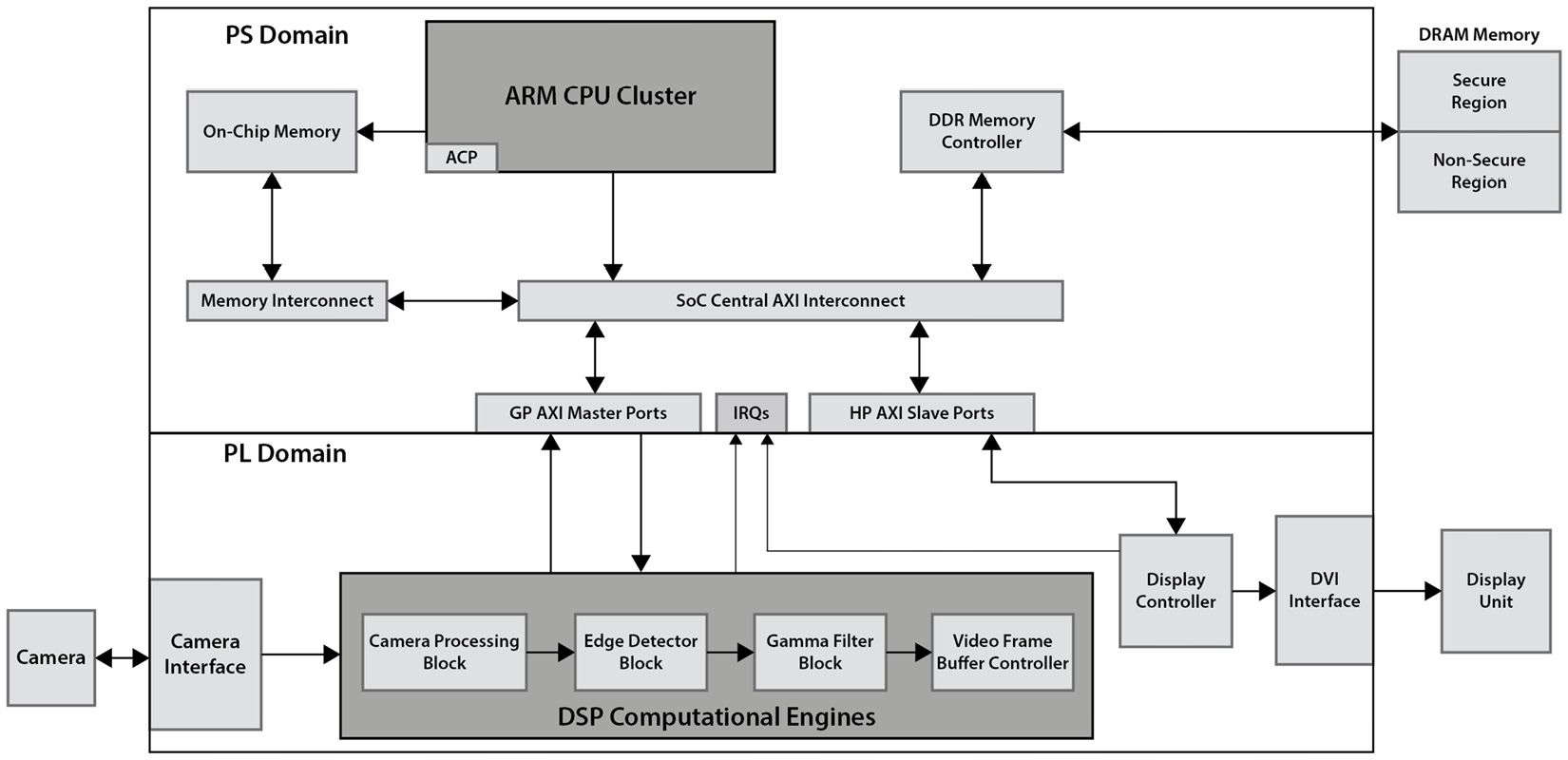
Figure 13.9 – Edge detection video application architecture example in an FPGA SoC
The preceding architecture provides a powerful platform for edge detection video applications and optimizes the overall device cost and power consumption.
Using an SoC-based FPGA for machine vision applications
The Zynq-7000 SoC FPGA is an ideal platform for implementing an HP machine vision algorithm such as the MVTec HALCON. The vision-based processing can be offloaded to the Programmable Logic (PL) portion of the SoC FPGA and achieves orders of magnitude of improvement of software-only-based machine vision processing. The following architecture can be implemented in the Zynq-7000 SoC FPGA:
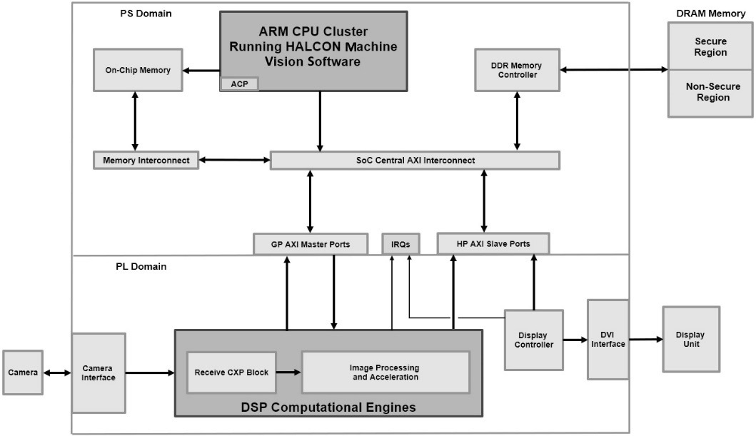
Figure 13.10 – Machine vision application architecture example in an FPGA SoC
This architecture accelerates the vision processing with visual applets implemented in the PL portion of the FPGA SoC and HALCON software running on the Cortex-A9 in the PS. It exceeded 90 frames/second in a machine vision model for an industrial application for manufactured parts inspection. This acceleration is around 20x faster in comparison to a software-only-based machine vision application.
Information
The preceding architecture example is provided in a Xilinx white paper. Further details on this specific video application can be found at https://docs.xilinx.com/v/u/en-US/wp453-machine-vision.
Summary
In this chapter, we looked at some advanced applications where FPGA-based SoCs are well suited as a single-chip architecture with a fast time to market product development and a lower cost solution, which is also lower power in comparison to multi-chip-based architectures. These advanced applications find many uses in DSP and video and image processing systems. Like the generic hardware acceleration capabilities of FPGA-based SoCs, DSP applications are well suited to these types of devices. SoCs built using PL have tight integration between the Cortex-A9 CPU cluster and the PL. This flexible architecture offers a scalable DSP solution where the exact amount of compute capabilities is used. Designers can start with a pure software solution, then they can offload heavy-compute DSP and video and image processing algorithms to the FPGA logic, which is rich in DSP building blocks. We examined the intrinsic DSP capabilities of the Cortex-A9 CPU, which make use of the Advanced SIMD feature of the ARM architecture implemented under the name NEON. These use vectors of multiple datasets upon which the same operation is simultaneously executed. We also looked at the case of multiple parallel vector operations being needed to improve the performance of the Cortex-A9 NEON engine and how this can be achieved using the DSP building blocks in the FPGA logic. We looked at a generic video and image processing system architecture and its different building blocks. We also looked at a few video and image processing applications and how they can be implemented in an FPGA SoC. We saw that many applications in the video and image processing domain are well suited for SoC FPGA implementation where heavy algorithms compute engines are built using the FPGA logic DSP resources and the software management and orchestration are running on the Cortex-A9 CPU. We then looked at two example architectures using the Zynq-7000 SoC FPGA, the first for edge detection and the second for machine vision.
In the next chapter, we will explore more topics related to the FPGA-based SoC advanced applications with a focus on communication and control systems.
Questions
Answer the following questions to test your knowledge of this chapter:
- List the advantages of using an FPGA-based SoC to implement a system with the heavy use of mathematical algorithms in a DSP application.
- Describe the process of deciding whether offloading the DSP computation to the FPGA logic is the correct decision to make. You can refer to the hardware acceleration methodologies described in the previous chapters.
- Define SIMD and describe how it can improve the software runtime performance and reduce power consumption.
- List some of the challenges you may face if you decide to use a CPU SIMD feature.
- What does NEON refer to in the ARM architecture and how wide are the datasets its instruction set can operate on?
- How could you extend the NEON capabilities of the Cortex-A9 CPU in a Zynq-7000 SoC FPGA? Name the main logic resources you would use to achieve this.
- Draw a simple SoC diagram where you offload heavy DSP algorithms to the FPGA logic, showing both the data path and the control path.
- Describe the minimal system architecture of a video processing system. Does every video processing system need to have all the listed subcomponents?
- What is the Xilinx VDMA engine? How different it is from a central DMA engine for moving regular data in the SoC?
- What is an edge detection video application? List its major architecture components.
- Which components of the edge detection video processing application are well suited for the FPGA logic implementation? Can you explain why?
- Name one of the machine vision algorithms. What kind of performance improvement should we expect when we offload its heavy compute algorithms from the Cortex-A9 CPU to a DSP engine implemented in the FPGA logic?