1 Hardware of the PIC16F648A-Based PLC
The hardware of the PIC16F648A-based programmable logic controller (PLC) consists of two parts: the CPU board and the I/O extension board. The schematic diagram and the photograph of the PIC16F648A-based PLC CPU board are shown in Figures 1.1 and 1.2, respectively. The CPU board contains mainly three sections: power, programming, and CPU (central processor unit)
The power section accepts 12 V AC input and produces two DC outputs: 12 V DC, to be used as the operating voltage of relays, and 5 V DC, to be used for ICs, inputs, etc. The programming section deals with the programming of the PIC16F648A microcontroller For programming the PIC16F648A in circuit, it is necessary to use PIC programmer hardware and software with In Circuit Serial Programming (ICSP) capability For related hardware and software to be used for programming the PIC16F648A-based PLC, please visit the following web page: http://www.meliksah.edu.tr/muzam/. For other types of USB, serial, or parallel port PIC programmers the reader is expected to make necessary arrangements The ICSP connector takes the lines VPP(MCLR), VDD, VSS(GND), DATA (RB7), and CLOCK (RB6) from the PIC programmer hardware through a properly prepared cable, and it connects them to a four-pole double-throw (4PDT) switch There are two positions of the 4PDT switch As seen from Figure 1.1, in one position of the 4PDT switch, PIC16F648A is ready to be programmed, and in the other position the loaded program is run For properly programming the PIC16F648A by means of a PIC programmer and the 4PDT switch, it is also a necessity to switch off the power switch. The CPU section consists of the PIC16F648A microcontroller In the project reported in this book, the PLC is fixed to run at 20 MHz with an external oscillator. This frequency is fixed because time delays are calculated based on this speed By means of two switches, SW1 and SW2, it is also possible to use another internal or external oscillator with different crystal frequencies When doing so, time delay functions must be calculated accordingly SW3 connects the RA5 pin either to one pole of the 4PDT switch or to the future extension connector When programming PIC16F648A, RA5 should be connected to the 4PDT switch RB0, RB6, and RB7 pins are all reserved to be used for 8-bit parallel-to-serial converter register 74HC/LS165. Through these three pins and with added 74HC/LS165 registers, we can describe as many inputs as necessary. RB0, RB6, and RB7 are the data in, clock in, and shift/load pins, respectively. Similarly, RB3, RB4, and RB5 pins are all reserved to be used for 8-bit serial-to-parallel converter register/driver TPIC6B595 Through these three pins and with added TPIC6B595 registers,
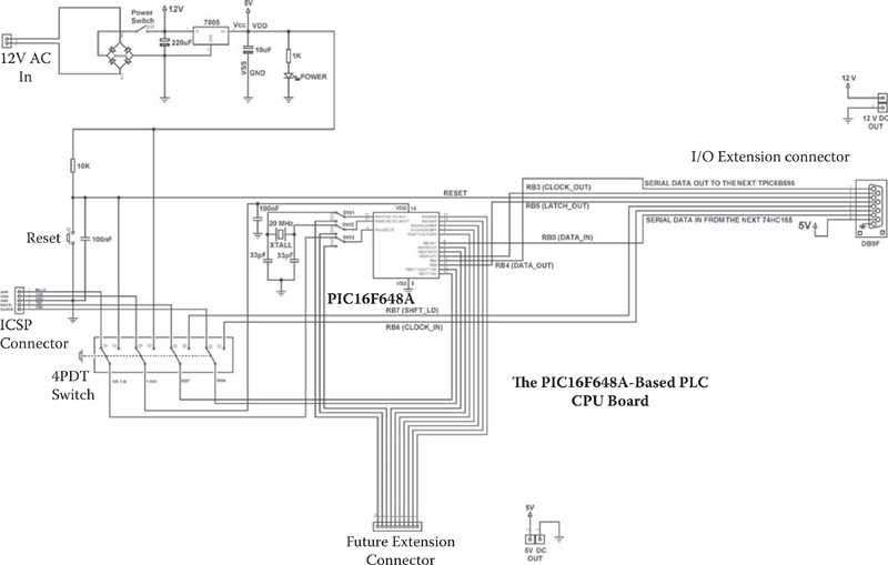
FIGURE 1.1
Schematic diagram of the CPU board.
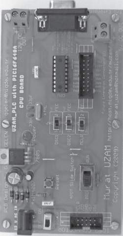
FIGURE 1.2
Photograph of the CPU board.
we can describe as many outputs as necessary. RB3, RB4, and RB5 are the clock out, data out, and latch out pins, respectively. The remaining unused pins of the PIC16F648A are connected to the future extension connector. PIC16F648A provides the following: flash program memory (words), 4096; RAM data memory (bytes), 256; and EEPROM data memory (bytes), 256. The PIC16F648A-based PLC macros make use of registers defined in RAM data memory. Note that it may be possible to use PIC16F628A as the CPU, but one has to bear in mind that PIC16F628A provides the following: flash program memory (words), 2048; RAM data memory (bytes), 224; and EEPROM data memory (bytes), 128. In that case, it is necessary to take care of the usage of RAM data memory
Figures 1.3 and 1.4 show the schematic diagram and photograph of the I/O extension board, respectively. The I/O extension board contains mainly two sections: eight discrete inputs and eight discrete outputs The I/O extension connector DB9M seen on the left connects the I/O extension board to the CPU board or to a previous I/O extension board. Similarly, the I/O extension
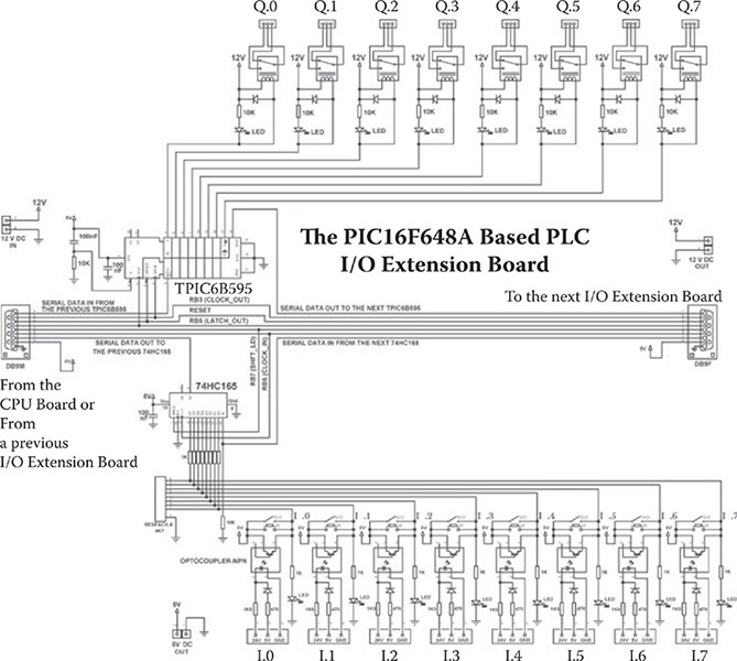
FIGURE 1.3
Schematic diagram of the I/O extension board.
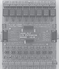
FIGURE 1.4
Photograph of the I/O extension board.
connector DB9F seen on the right connects the I/O extension board to a next I/O extension board. In this way we can connect as many I/O extension boards as necessary. Five-volt DC and 12 V DC are taken from the CPU board or from a previous I/O extension board, and they are passed to the next I/O extension boards. All I/O data are sent to and taken from all the connected extension I/O boards by means of I/O extension connectors DB9M and DB9F.
The inputs section introduces eight discrete inputs for the PIC16F648A-based PLC (called I0.0, I0.1, I0.7 for the first I/O extension board). Five-volt DC or 24 V DC input signals can be accepted by each input These external input signals are isolated from the other parts of the hardware by using NPN type opto-couplers (e. g., 4N25). For simulating input signals, one can use onboard push buttons as temporary inputs and slide switches as permanent inputs In the beginning of each PLC scan cycle (get_inputs) the 74HC/LS165 is loaded (RB7 (shift/load) = 0) with the level of eight inputs and then these
FIGURE 1.5
Schematic diagram of the CPU board plus two I/O extension boards.
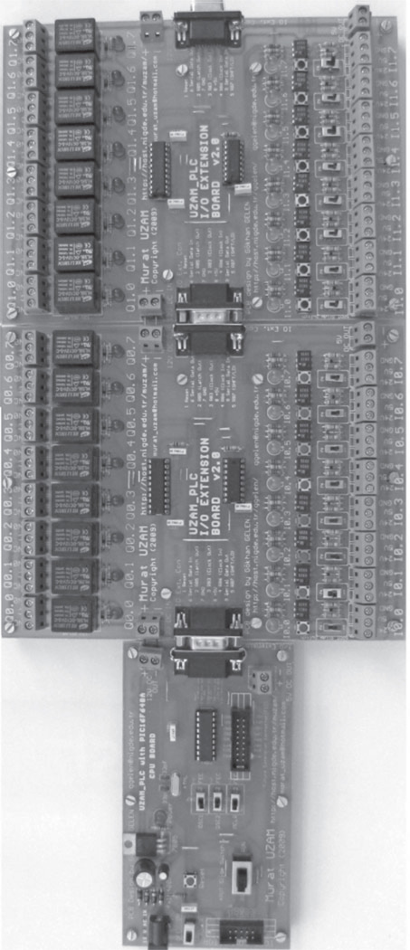
FIGURE 1.6
Photograph of the CPU board plus two I/O extension boards.
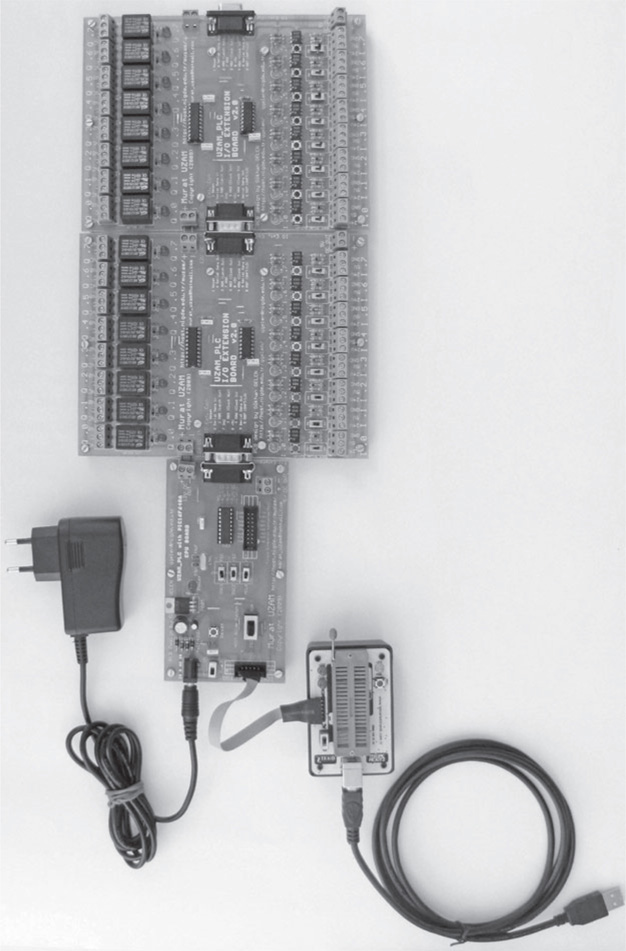
FIGURE 1.7
Photograph of the CPU board plus two I/O extension boards and a USB PIC programmer.
data are serially clocked in (when RB7 = 1; through RB0 data in and RB6 clock in pins). If there is only one I/O extension board used, then eight clock_in signals are enough to get the eight input signals. For each additional I/O extension board, eight more clock_in signals are necessary. The serial data coming from the I/O extension board(s) are taken from the SI input of the 74HC/LS165
The outputs section introduces eight discrete relay outputs for the PIC16F648A-based PLC (called Q0.0, Q0.1, Q0.7 for the first I/O extension board). Each relay operates with 12 V DC and is driven by an 8-bit serial-to-parallel converter register/driver TPIC6B595 Relays have single-pole double-throw (SPDT) contacts with C (common), NC (normally closed), and NO (normally open) terminals. At the end of each PLC scan cycle (send_outputs) the output data are serially clocked out (through RB3 clock out and RB4 data out pins) and finally latched within the TPIC6B595. If there is only one I/O extension board used, then eight clock_out signals are enough to send the eight output signals. For each additional I/O extension board, eight more clock_out signals are necessary The serial data going to the I/O extension board(s) are sent out from the SER OUT (pin 18) of the TPIC6B595
The PCB design files of both the CPU board and the I/O extension board can be obtained from the CD-ROM attached to this book Note that in the PCB design of the CPU board and the I/O extension board, some lines of I/O extension connectors DB9M and DB9F are different from the ones shown in Figures 1.1 and 1.3.
The project reported in this book makes use of a CPU board and two I/O extension boards, as can be seen from the schematic diagram and photograph depicted in Figures 1.5 and 1.6, respectively. Thus, in total there are 16 inputs and 16 outputs. Figure 1.7 shows the PIC16F648A-based PLC consisting of a CPU board, I/O extension boards, 12 V DC adapter, and USB PIC programmer.