Finalizing the Design
POSTROUTING INSPECTION
Depending on how you placed your parts, your board might look something like
Figure 9-81
(not all layers shown). After the autorouter has finished routing the board, it should be checked for problem areas, such as acute angles, long parallel traces, and bad via locations.
Chapter 6
discusses several of these and other routing issues. It is also necessary to check for new DRC errors that may have been caused by the routing process and check for any nets that the autorouter could not route.
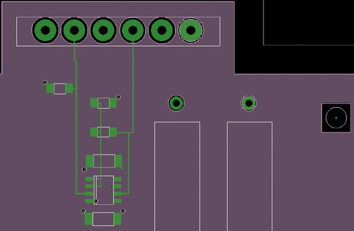 |
| Figure 9-81 Board design after final parts placement and autorouting. |
CHECKING ROUTING STATISTICS
Once you have all the traces routed, you can check for new DRC errors and unrouted nets using the
Status dialog box (
Figure 9-82
).
To view routing statistics, select
Display → Status from the menu bar. The
Status dialog box provides information about the number of unrouted nets as well as unplaced components.
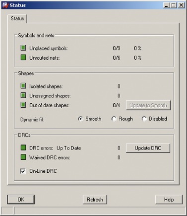 |
| Figure 9-82 Use the
Status dialog box to check for unrouted nets and DRC errors. |
If the routing statistics are less than 100% but you cannot easily locate unrouted nets, use the
Visibility filter tab to turn off all Etch layers and make sure that the
Rats All button is active,
 . Use the
Find filter (look for nets only) and the Show Element tool and drag a box across the board area. Any unrouted nets should be displayed in the
Show Element text box with information about the net’s name, to which pins the net belongs, and its location. An example is shown in
Figure 9-83
.
. Use the
Find filter (look for nets only) and the Show Element tool and drag a box across the board area. Any unrouted nets should be displayed in the
Show Element text box with information about the net’s name, to which pins the net belongs, and its location. An example is shown in
Figure 9-83
.
| Rats All button
|
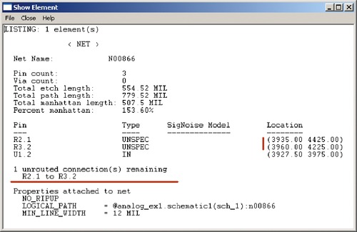 |
| Figure 9-83 Using the
Find filter and Show Element tool to identify unrouted nets. |
CLEANING UP A DESIGN BY GLOSSING
After the autorouter has finished routing the board (or after performing any last-minute manual routing tasks), you can have PCB Editor go over the design and perform a cleanup using the Gloss command.
To clean up (gloss) a board design, select
Route → Gloss… from the menu. At the
Line Smoothing dialog box (see
Figure 9-84
), check the options you would like PCB Editor look for and fix. When you have made your selections, click the
Gloss button.
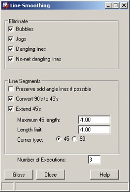 |
| Figure 9-84 Use the Gloss command to add finishing touches to the board design. |
You can attach either the NO_GLOSS property or the FIXED property to the nets so that gloss does not modify the routing of these nets. Use the Constraint Manager to apply the NO_GLOSS property to a net. Select the
Properties tab and the
Net/General Properties icon then set the NO_GLOSS property to
On. To apply the FIXED property, you can also use the Constraint Manager or use the
Fix button on the toolbar.
SYNCHRONIZING THE DESIGN WITH CAPTURE (BACK ANNOTATION)
Once the board design is finished, you can export information from your PCB design to your schematic by performing a back annotation. Back annotation in PCB Editor is called
feedback (search for it in
fcoms.pdf). Also see
Backannotating to Allegro Design Entry HDL or System Connectivity Manager in
Transferring Logic Design Data (algrologic.pdf), and the
Capture User’s Guide (cap_ug.pdf). See
Back annotation from PCB Editor, p. 508.
Information that is back annotated has to be common to PCB Editor and Capture. To see some examples of these properties, go to the schematic page and double click a part to display the properties spreadsheet. Select the
Cadence-Allegro filter. Some examples are
HARD_LOCATION,
NO_SWAP_GATE,
NO_SWAP_PIN. The configuration file
allegro.cfg, which is located in the
C:OrCADOrCAD_16.0 oolscapturepath by default, lists all of the properties included during back annotation.
To perform a back annotation from PCB Editor to Capture, go to the PCB design in PCB Editor and select
Setup → User Preferences…. In the
User Preferences dialog box, left click the
Logic folder once, and select
capture in the
schematic_editor: list, as shown in
Figure 9-85
.
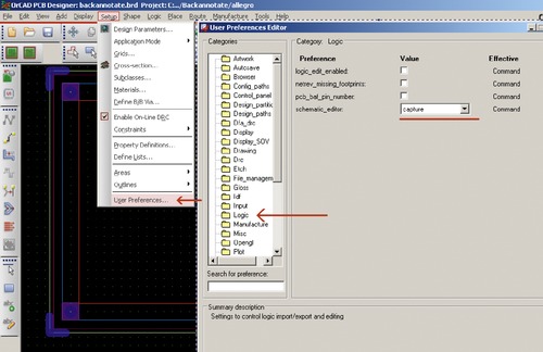 |
| Figure 9-85 Setting the
Logic type for back annotation. |
From the
File menu, select
Export Logic…; the
Export Logic dialog box will be displayed (see
Figure 9-86
). Select the
Cadence tab, select the
Design entry CIS option, and select the destination path from
Export to directory: area (use the
Browse… button). The default path is your current working directory, displayed in the
Export to directory field as a period (unless another location was specified and applied in a previous session). Click the
Export Cadence button. That’s it for PCB Editor. Now go back to Capture to import the back-annotation information into the project design.
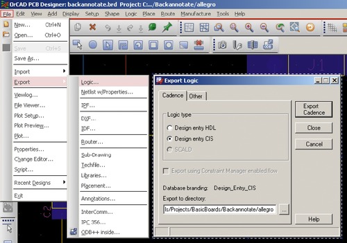 |
| Figure 9-86 Displaying the
Export Logic dialog box. |
In Capture go to the
Project Manager pane and select the
Project icon. Then select
Back Annotate… from the
Tools menu, as shown in
Figure 9-87
.
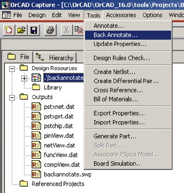 |
| Figure 9-87 Performing back annotation in Capture. |
The
Backannotate dialog box will be displayed. Select the
PCB Editor tab and select the proper files and paths using the
Browse… buttons. You can change what gets imported by clicking the
Setup… button, as shown in
Figure 9-88
. The
allegro.cfg file lists the parameters that will be imported. To edit the file, click the
Edit button on the
Setup dialog box. If you edit the file, remember to save the changes. Dismiss the .cfg file and Click
OK three times to dismiss the dialog boxes and perform the back annotation.
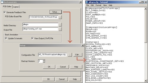 |
| Figure 9-88 Setting up the back-annotation path and
allegro.cfg file. |
To see what changes were made, double click a part in the schematic to view the properties sheet. Select
Cadence-Allegro from the
Filter by: list.
Figure 9-89
shows the trace width properties that were set in the Constraint Manager in PCB Editor (a) are imported into the
Edit Properties spreadsheet in Capture (b).
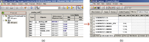 |
| Figure 9-89 Net properties back annotated to (a) PCB Editor (b) Capture from. |
This completes the first example. At this point you would produce the manufacturing files for the board and send them off to a board house for manufacturing. We look at this in greater detail in
Chapter 10
.
..................Content has been hidden....................
You can't read the all page of ebook, please click here login for view all page.