
Chapter 6. PCB Design for Signal Integrity
Desirable electrical characteristics of a circuit and its PCB include low noise, low distortion, low cross talk, and low radiated emissions, to name a few. The purpose of this chapter is to introduce the issues that cause PCB performance problems and how to route the PCB to minimize them and maximize signal integrity.
Circuit Design Issues Not Related to PCB Layout
Circuit design constraints are primarily the responsibility of the circuit design engineer and will not be covered in detail here, but some of the issues will be mentioned briefly since the symptoms of poor circuit design can be confused with PCB design problems.
Noise
Noise generally refers to any signal that interferes with or degrades a signal of interest. It is often used with an adjective for problems, such as phase noise, switching noise, cross-talk noise, and reflection noise. In this text we will limit the term
noise to mean random or pseudo-random, natural signals, which are generally not a result of the PCB design. Functional problems such as cross talk or ringing (which are PCB-related problems) will be named as such. From this perspective there are two basic categories of noise: background noise and intrinsic component noise. These noise problems are generally addressed by the circuit designer, not the PCB designer, but are discussed here briefly for completeness.
BACKGROUND NOISE
Background noise is an uncontrolled signal that originates from the system or environment your board is working in. For example, if your circuit is an audio amplifier that is supposed to amplify a speaker’s voice as he or she speaks into a microphone, but a crowd of people is talking around the speaker or a jet plane flies overhead, both the speaker’s voice and the background sounds will be amplified and the signal would be considered noisy or said to suffer from a low signal-to-noise ratio. There is nothing you can do about it from the PCB design perspective. Sensors may also be noisy because of their sensitivity, but that is also a circuit design issue and needs to be handled long before the PCB is laid out.
INTRINSIC NOISE
There are four basic types of intrinsic noise: thermal noise, shot noise, contact noise, and popcorn noise. Thermal noise (also known as
Johnson noise) is due to the motion of electrons in a conducting material. It is present in any material that exhibits a resistance to current flow and is a function of temperature. It is white noise (is constant over frequency) and is prominent in resistors and semiconductor devices. Shot noise is also white noise and is due to potential barriers and is also prevalent in semiconductor devices.
Contact noise (also called
excess noise in resistors and l/
f noise) is due to imperfect connections at contact junctions or interfaces. It is not constant over frequency and can be fairly large at low frequencies. Your best defense against this type of noise is good-quality connectors and good solder joints.
Popcorn noise (also called
burst noise) is typically proportional to l/
f2 and is worse in high-impedance circuits. It is caused by manufacturing defects in semiconductors and ICs.
Distortion
Distortion is an issue more related to analog circuitry because of the nature of continuous signals. In analog circuitry all voltages between the power supply rails may be of significance. Digital signals are not continuous: they are either HI or LO and usually nothing in between matters. As long as voltage levels meet threshold specifications, there is no ambiguity and therefore no quality issues. Ringing on the rising and falling edges of a square wave might be considered distortion, but that is handled differently, as described below. Distortion of a sinusoidal signal (which normally has a single spike on a frequency spectrum) begins to occur in amplifiers as the sine waves either are clipped or experience a phase reversal. Op amps have amplitude limits imposed by the power supplies, their drive capabilities, and their frequency response. If the amplitude of a sinusoidal output signal (as determined by the input signal times the gain) exceeds the output capability of the op amp, then the output signal will be clipped off and begin to resemble a square wave. Square waves are composed of many sine waves, which are primarily odd harmonics of the fundamental frequency of the square wave. The dominant harmonic is typically the third one, so as a sine wave begins to clip the onset of third harmonic distortion is observed.
If the input signal exceeds the op amp’s input limits (as imposed by the power supply rails), the output signal will also be distorted. Some amplifiers simply clip the signal (causing third harmonic distortion), while other op amps experience phase inversion, which also causes harmonic distortion.
These problems are caused by the circuit design and component selection and are not the fault of the PCB design. These effects are mentioned because, if you are not used to them or do not know about them, they can be confused with PCB layout problems. Along with harmonic distortion ringing will produce unwanted frequency components, which can be seen with a spectrum analyzer and may be confused with other forms of distortion or noise. Ringing is caused by reflections, which in turn are caused by impedance mismatches on PCB traces, which
is a function of the PCB design.
Frequency Response
Both analog and digital circuits have frequency limits. In digital circuitry, if frequency limits are exceeded the signal level may rise and fall before a gate has a chance to switch states. This may give the appearance that the signal is attenuated or that the receiving gate is “not seeing” the signal. This too is a circuit design problem and not a PCB problem. In circuit design we need to make sure that the components selected are within design constraints.
When signals exceed the frequency limits of analog circuitry, the output signal will also be attenuated, and distortion will result if the sine wave begins to look like a triangle wave at the output of the frequency-limited component. This is a function of the amplifier’s slew rate, −3
dB BW, and gain bandwidth product. Again these issues need to be handled at the circuit design level, well before the PCB design stage.
Issues Related to PCB Layout
Electromagnetic Interference and Cross Talk
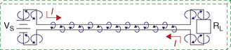
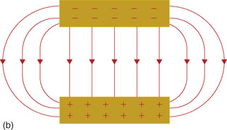
There are three goals in designing PCBs for electrical performance and signal integrity: (1) The PCB should be immune from interference from other systems, (2) it should not produce emissions that cause problems for other systems, and (3) it should demonstrate the desired signal quality. A common factor relating these three issues is electromagnetic waves. As Figure 6-1 shows, “noise” can be introduced into your PCB from outside sources, and it can produce noise that is radiated to other systems and to itself.
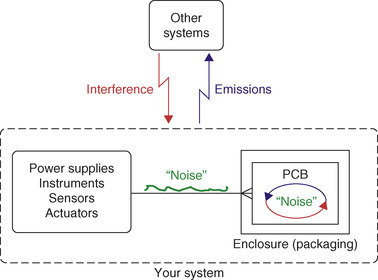 |
| Figure 6-1 The enemy—electromagnetic interference. |
When electromagnetic waves get into your system, this is referred to as
electromagnetic interference (EMI). On the flip side, your PCB can be the source of EMI and cause problems for other systems. The ability for systems to “play nice together” is referred to as
electromagnetic compatibility (EMC). The FCC has established rules for many types of systems regarding EMI and EMC, which, depending on your application, your PCB may have to abide by. Properly laying out your PCB can greatly reduce EMI and improve EMC. In this section we take a look at how to minimize EMI and its effects. There are many good books available that address these issues in greater detail. The material in this chapter is not intended to duplicate those works but to provide an overview of the issues and provide insight on how to design PCBs with PCB Editor with regard to signal integrity issues.
The method by which systems and circuits can “reach out and touch” another circuit is inductive and capacitive coupling of electromagnetic fields.
In the 1820s Faraday and Henry showed that an electric current could be produced in a conductor by changing the current in another, nearby conductor (Serway 1992, p. 806). And years later Maxwell showed that changing electric fields also produce magnetic fields. These fields are the source of many woes in PCB design. We begin by looking at magnetic fields and inductive coupling.
Magnetic Fields and Inductive Coupling
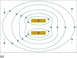
As shown in Figure 6-2 a magnetic field vector, B, is developed around a conductor when current flows through the conductor, into the “X” end and out of the “Dot” end of the conductor. The right-hand rule (from Ampere’s law) is used to determine the direction of the field: If the thumb of the right hand points in the direction of conventional current flow (movement of positive charges), then the magnetic field curls in the direction of the fingers. This is defined mathematically by a cross product called the
Biot-Savart law. By applying some calculus, which will not be shown here, an equation can be derived for the scalar (nonvector) magnitude,
B, of the magnetic field vector, B, near the conductor.
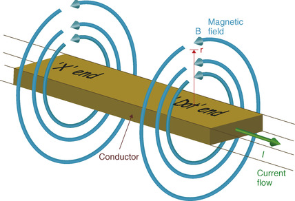 |
| Figure 6-2 Magnetic field caused by a current-carrying conductor. |
The magnitude of the magnetic field a distance,
r, from a long straight conductor (Serway 1992, p. 838) is given by Eq. (6.1),
 where
B is the magnitude of the magnetic field in Wb/m
2, μ
0 is the permeability of free space (μ
0 = 4π × 10
−7Wb/A×m),
I is the current in amps (A), and
r is the distance from the conductor.
where
B is the magnitude of the magnetic field in Wb/m
2, μ
0 is the permeability of free space (μ
0 = 4π × 10
−7Wb/A×m),
I is the current in amps (A), and
r is the distance from the conductor.
(6.1)
The total magnetic field within or through an area is called magnetic flux, Φ, which has units of Wb and is described by Eq. (6.2) (Serway 1992, p. 849; Wb/m
2 × m
2 = Wb),
 where
B is the magnetic field magnitude per unit area (Wb/m
2),
A is the area intersected by the magnetic field (m
2), and θ is the angle between
B and
A.
where
B is the magnetic field magnitude per unit area (Wb/m
2),
A is the area intersected by the magnetic field (m
2), and θ is the angle between
B and
A.
(6.2)
Magnetic flux expands or contracts in proportion to changes in current flow. As the flux expands or contracts around the conductor, we see from Faraday’s Law of Induction, given in Eq. (6.3) (Serway 1992, p. 877), that a voltage is induced into the conductor. This is known as
self-induced electromotive force (emf):

(6.3)
The minus sign in Eq. (6.3) is a result of Lenz’s law, which states that the emf induced into the conductor produces a current in the conductor that creates a magnetic flux that will oppose the changing magnetic flux. This effect is called
self-inductance. The self-inductance tends to limit how fast the current can change in a conductor. This is what makes an inductor have inductance and oppose AC currents in analog circuits and fast rise times in digital circuits. The magnitude of the inductance,
L, is shown in Eq. (6.4):

(6.4)
The inductance is directly proportional to
N, the number of turns on a coil (
N=1 for a PCB trace and its return path), and the magnetic flux and is inversely proportional to the current,
I.
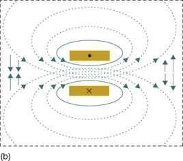
If a secondary conductor is near a primary conductor, which is carrying current as shown in Figure 6-3, some of the flux will be felt by the secondary conductor. If the current through the primary conductor changes with respect to time (as in the case of a rising edge of a digital signal or an AC signal) the magnetic field (and therefore the magnetic flux) also changes with respect to time as it increases in strength and expands outward (or decreases in strength and contracts inward) from (or toward) the primary conductor.
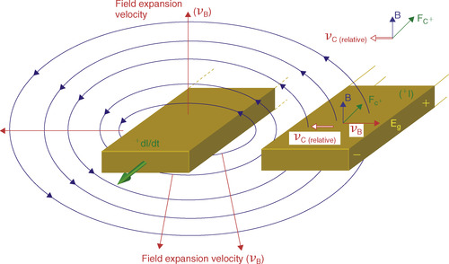 |
| Figure 6-3 Voltage induced into adjacent trace by varying magnetic fields. |
When the flux that is impinging on the secondary conductor changes with respect to time, as it expands or contracts, we see again from Faraday’s Law of Induction in Eq. (6.3) that a voltage,
E
g, is induced into the secondary conductor. Using the right-hand rule for electric generators, the direction of the induced current can be determined. To use the right-hand rule point the thumb in the direction of the motion of the conductor (relative to the expanding/shrinking flux—ν
C), point the first finger in the direction of the
B field, and the middle finger will point in the direction of the force applied to the positive charges
 and therefore the positive current flow. The resultant voltage and current are shown in Figure 6-3. Notice that the current in the secondary conductor flows in the direction opposite that of the current in the primary conductor as a result of the induced voltage. This produces a secondary magnetic field which opposes and partially cancels the primary magnetic field (by Lenz’s law).
If the induced current flow in the secondary conductor is changing with respect to time (which it is because the primary conductor is causing it to) and it is in close proximity to the first conductor (which it is), then the secondary conductor will also induce an emf back into the primary conductor. The magnetic flux that goes back and forth between the two conductors is called
mutual inductance.
The emf (voltage) generated into the primary conductor (by the secondary conductor) will be in a direction that aids the original current flow in the primary conductor as the secondary flux tries to oppose the primary flux. If the original flux is partially canceled, then the self-inductance is also partially canceled and the changing current in the primary conductor is not as limited (i.e., it sees less inductance).
It would seem that unlimited current could flow in the primary inductor since the secondary conductor aids it, but the secondary inductor also experiences its own self-inductance and is therefore limited. Also the amount of mutual inductance between the two conductors is limited by how much of the flux couples the two conductors. This is similar to the coupling coefficient in transformers and in both circumstances is never 100%.
When a trace on a PCB induces a voltage into an adjacent signal trace we call that
cross talk, which is bad because it generates noise in the adjacent signal trace. But if the second conductor is the PCB’s ground plane, that is good because it reduces the trace’s inductance and therefore the overall
loop inductance of the circuit. For the time being we will stick with using the term
return plane, rather than
ground plane, for reasons described later.
Loop Inductance
In Figure 6-3 only segments of the traces were shown. Of course for current to flow through the circuit, a closed path must exist, as shown in Figure 6-4. Any conductor in the circuit that carries current will produce a magnetic field as indicated by the circular arrows.
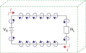 |
| Figure 6-4 Loop inductance of a closed circuit. |
An equation for inductance is given in Eq. (6.5) (Serway 1992, p. 905),
 where
n is the number of turns (1),
A
where
n is the number of turns (1),
A is the volume that the circuit occupies, and μ
0 is the relative permeability of the material in which the circuit exists. For most materials used in PCBs, μ
0 = 1. So the inductance is a function of the volume of the inductor and the number of turns of the conductor around the space. Therefore, inductance is dependent on the circuit geometry, by which a smaller volume results in a smaller circuit or loop inductance.
is the volume that the circuit occupies, and μ
0 is the relative permeability of the material in which the circuit exists. For most materials used in PCBs, μ
0 = 1. So the inductance is a function of the volume of the inductor and the number of turns of the conductor around the space. Therefore, inductance is dependent on the circuit geometry, by which a smaller volume results in a smaller circuit or loop inductance.
(6.5)
If we look at the closed loop circuit shown in Figure 6-4 with respect to its volume, we can see that, if the circuit is physically large and makes a large loop, it will have what is referred to as high loop inductance.
If on the other hand we arrange the circuit as shown in Figure 6-5, we can see from Eq. (6.5) that the loop inductance will be less since there is less volume. If you notice the direction of the arrows (the magnetic fields) you can see that the source current and the return current magnetic fields oppose each other, thereby reducing the flux and inductance.
 |
| Figure 6-5 Closed loop circuit with low loop inductance. |
Figure 6-6(a) shows the resultant magnetic field of two conductors in close proximity where the currents are in the same direction. As indicated the magnetic fields circulate in the same direction and aid each other. This is the case for an inductor in which the turns are wound in the same direction and build up an overall strong magnetic field.
 |
 |
| Figure 6-6 Aiding and opposing magnetic fields: (a) aiding fields, (b) opposing fields. |
Figure 6-6(b) shows the resultant magnetic field when the currents of the two conductors are in opposite directions. The magnetic fields oppose each other and result in partial flux cancellation. The amount of cancellation depends on the amount of mutual inductance, which in turn depends in part on the distance between the conductors.
The situations in Figure 6-4Figure 6-5 and Figure 6-6 are steady-state DC circuits, but if we apply the concept in Figure 6-3 and Eq. (6.3) for time-varying currents, then we can see that, if the return trace on a circuit board is in close proximity to the signal trace, then the inductance of the traces is reduced; that is, the loop inductance of the closed-loop circuit is reduced. If the loop inductance is reduced in an AC circuit, then by Eq. (6.6) it can be seen that there will be less inductive reactance (
X
L), less voltage drop, and less cross talk (fewer EMI problems):

(6.6)
To maintain a small
X
L (and low loop inductance), we need to have the return path as wide as possible (low self-inductance) and as close as possible to the signal path wherever possible (maximum coupling and small cross-sectional areas). The easiest way to do this is by using a plane layer as the return path. The return plane has historically (and most often inappropriately) been called the
ground plane, but it is being referred to more often as an
image plane or a
return plane. In PCB design a return plane has low inductance (and therefore low self-inductance) and it is everywhere the signal trace is and therefore allows for maximum coupling between the signal trace and the plane for any and all widths of the signal trace.
From this discussion then we can say that one of the most important functions of the return (image) plane is to reduce loop inductance. Reducing loop inductance (and the magnetic fields related to it) provides a low-impedance return path for power and signal lines and reduces unwanted cross talk to nearby conductors. It should also be stated that cross talk between unrelated conductors is also reduced by keeping them farther apart (i.e.,
r is large).
Electric Fields and Capacitive Coupling
We saw in the previous paragraphs that keeping signal and power lines close to their return paths provides flux cancellation and reduces loop inductance, which is beneficial in all respects. But what happens with the electric fields under these circumstances and what is the effect on the circuit?Figure 6-7(a) shows electric field lines for a single charged conductor, which can represent a signal trace that is a long way away from its return path. Figure 6-7(b) shows electric field lines between two oppositely charged conductors, which can represent a signal or power line close to its return path. As shown, the solitary conductor radiates electric field lines in all directions, while the coupled conductors contain (or at least concentrate) the electric field between them.
 |
 |
| Figure 6-7 Electric fields on conductors: (a) a single charged conductor, (b) a field between oppositely charged conductors. |
The Ampere–Maxwell law (Serway 1992, p. 851) states that “magnetic fields are produced both by conduction currents and by changing electric fields.” So, to minimize cross talk, it would seem to be in our best interest not to allow traces to radiate electric fields in an uncontrolled manner but to keep the signal (and power) traces close to their return paths. This is true for both magnetic and electric fields.
But what happens to the capacitance of the traces relative to the return plane when we do this? The equation of a parallel plate capacitor (in farads) in air is given in Eq. (6.7) (Serway 1992, p. 712),
 where
C is capacitance (in farads), ε
0 is permittivity of free space,
A is the area common to the parallel plates, and
d is the distance between the plates. As indicated, as the plates become closer together or as the area becomes larger, the capacitance increases. This also holds for the capacitance between a trace and the return plane, although as we will see later the equation is slightly different and the units are in F/in. to make it easier to calculate capacitance for various trace lengths.
where
C is capacitance (in farads), ε
0 is permittivity of free space,
A is the area common to the parallel plates, and
d is the distance between the plates. As indicated, as the plates become closer together or as the area becomes larger, the capacitance increases. This also holds for the capacitance between a trace and the return plane, although as we will see later the equation is slightly different and the units are in F/in. to make it easier to calculate capacitance for various trace lengths.
(6.7)
From Eq. (6.8) we can see that as the capacitance,
C, increases the capacitive reactance decreases:

(6.8)
By combining Eqs. (6.7) and (6.8) as shown in Eq. (6.9), we can see that, by keeping traces and power planes close to their return planes (small
d), the capacitive reactance between the trace and the return plane is reduced (coupling is increased):

(6.9)
And by keeping unrelated signal traces farther apart (large
d), the reactance between the traces is higher and the coupling (cross talk) is reduced. With both magnetic and electric fields, the wider the return path (the areas of the conductor), the better the coupling, and the closer the signal or power conductor is to the return plane, the better the coupling.
Ground Planes and Ground Bounce
What Ground Is and What It Is Not
In the previous discussion, the term
return plane was used instead of the term
ground plane. Unless the return plane is physically connected to the earth by some means, it really has nothing to do with “ground,” The ground symbol,
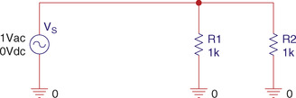
 , has long been used on schematics (in academia and in practice) to indicate a connection to the point to which all closed-circuit currents must return. An example is shown in Figure 6-8. This gives the impression that ground, somehow, is an omnipresent, unfaltering current sink and equipotential reference. Equipotential means that the voltage is the same everywhere, regardless of how much current is flowing through it. This is a myth.
| Ground Symbol
|
 |
| Figure 6-8 Typical depiction of “ground.” |
Although the depiction of the ground connection shown in Figure 6-8 is convenient to use on the schematic, in reality there has to be a physical, real-world connection. And, just so you know, the official ground symbols per IEEE Std 315-1975 (ANSI Y32.2-1975) are given in Table 6-1. The IEEE disclaims any responsibility or liability resulting from the placement and use in the described manner. However, it is quite common that the ground and return symbols are used otherwise. Since the ground concept has been around a long time, it is unlikely that its use will change overnight. The important thing is that it is clear what the symbol means. The standard states that the symbols can be given supplementary information (such as names) on the schematic to specifically annotate the symbol’s purpose or function.
| Symbols and definitions in Table 6-1 reprinted with permission from IEEE Std. 315-1975, Copyright 2003, by IEEE. All rights reserved. | ||
| Symbol | Name | Purpose/usage |
|---|---|---|
| Earth GND | A direct connection to the earth. | |
| A direct connection to a vehicle’s or an airplane’s frame that serves the same function as earth ground. | ||
| Noiseless GND | Used to indicate a low or noiseless earth ground. | |
| Safety GND | Used to indicate a ground connection that serves a safety function against electric shock. | |
| Chassis GND | A connection to a chassis, or frame, or similar connection of a printed circuit board and may be completely different from earth ground. | |
| Return | Used to indicate common return connections. | |
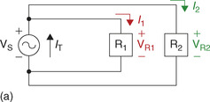
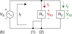
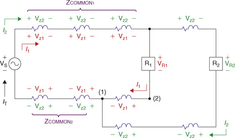
There are two basic ground and source connection schemes, parallel and series connections, as shown in Figure 6-9. A parallel ground system is shown in Figure 6-9(a). A parallel ground system is also called a
separate ground system, since the current flow in each branch is supplied by and returns to the source through completely separate paths. A series-connected ground system is shown in Figure 6-9(b). The series-connected ground system is also referred to as a
common ground system or
daisy chain, since the current flows in the two branches share a common path.
 |
 |
| Figure 6-9 Typical signal and return connection schemes: (a) parallel connected, (b) series connected. |
At the schematic level the circuits in Figure 6-9 are identical; mathematically the circuits are also identical, that is,
I
T =
I1 +
I2 and
V
R1 =
V
R2 =
V
s. Furthermore, as indicated in Figure 6-9(b), you could connect
R1 to the common return path at either point (1) or point (2) without changing the meaning of the circuit description in any way. However, on the PCB, the two circuits shown in Figure 6-9 can be significantly different. There may even be significant differences between points (1) and (2) in Figure 6-9(b).
It was said earlier that any conductor that carries current will produce a magnetic field. Even if there is very tight coupling between the signal conductor and its return conductor, some inductance will always exist because the coupling is not 100.0% complete; that is, there is less than perfect mutual inductance from the primary trace to the secondary trace (the return plane) and from the secondary trace back to the primary trace.
With this understanding we can see from Figure 6-10 that there is an “unseen” schematic within the PCB. As a result, although the relationship
I
T =
I1 +
I2 is still true, it should be realized that
V
R1 =
V
R2 =
V
s is no longer true because there are voltage drops along the shared and individual impedances between the source and each of the loads. Furthermore points (1) and (2) and any other points along the return path are not equipotential. The ideal, equipotential ground plane does not exist in practice.
 |
| Figure 6-10 The actual circuit—the hidden schematic. |
Common impedance is particularly troublesome when high-power or noisy signals share common return paths (
ZCOMMON1 and
ZCOMMON2) with low-power signals. High-speed digital signals operating near low-level analog signals are an example.
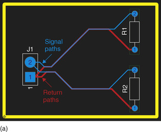
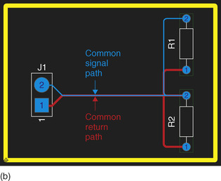
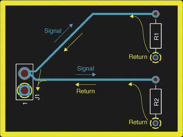
Clearly then, it would seem that the best return system is the parallel system shown in Figure 6-9(a). However, a potential problem arises when we try to implement this approach on the PCB. Figure 6-11 shows the routing scenarios in which Figure 6-11(a) is the parallel connection and Figure 6-11(b) is the series connection. As described above and shown in Figure 6-11(a), the current paths do not interfere with each other in the parallel connection since their paths are completely separate, and since each signal path is directly above its return path, there is tight coupling between the signal and the return and therefore the inductance is minimized. The problem is that it would become incredibly cumbersome to route a PCB using this approach with even a few additional components and worse on a high-density, multilayer PCB. If components are moved, movement of the signal and return paths would have to be carefully coordinated, resulting in many opportunities for routing “errors” that could be difficult to detect.
 |
 |
| Figure 6-11 Signal and return connection schemes in PCB Editor: (a) parallel (separate) connected, (b) series (common) connected. |
The series connection in Figure 6-11(b) is obviously much easier to route, but it loses the benefit of the separate signal and return paths. Even with the signal and return paths tightly coupled, the common paths (impedances) could be problematic for circuits operating at high frequency or with fast rise times.
Ground (Return) Planes
Above, we said that we want the return path to be as wide as possible and as “everywhere” as possible, which, when taken to the extreme, causes the return path to become a plane. But since (at first glance) it appears that a plane is potentially a common return path (a common impedance), the question arises as to whether this is really the best solution to overcome the inconvenience of the routing problem. If we reroute the circuit of Figure 6-8 as shown in Figure 6-12, in which the return path is the GND plane in PCB Editor (where the thermal reliefs indicate a connection to the GND plane), we can analyze the situation. If the signal path is relatively close to the return path, the return signal will automatically flow through the GND plane directly below the signal trace. The reason this happens is that by doing so the loop inductance of the circuit is minimized. As is commonly known in DC circuits, current follows the path of least resistance. Perhaps not as commonly known, AC currents will follow the path of least impedance and, particularly on PCBs, the path of least inductance. The only way for that to happen is if the return current travels directly under the signal trace on its way back to the source. This is true no matter what kind of crazy path the signal trace makes, as long as no discontinuities exist in the return plane.
 |
| Figure 6-12 Pseudo-common return path using a “ground” plane. |
So (in Figure 6-12) even if
R2 was directly between
R1 and the PCB connector, the return paths would not be common as long as the signal traces to
R1 and
R2 did not overlap (which can happen if the signal traces were routed on different layers) or become “too” close. We will look at the appropriate trace separation (what
too close means) in the routing section discussed later.
Ground Bounce and Rail Collapse
In a typical PCB the power distribution system contains one or more power and ground planes. The power and ground planes are like very wide traces (have little inductance) and are usually adjacent to each other (high capacitance). This is exactly what we want for the power distribution system. However, despite these advantages, a problem occurs in high-speed digital systems when gates switch from one state to another. The problem in general is known as
switching noise.
Figure 6-13 shows a representative CMOS logic gate. The capacitor,
C
L, represents all of the capacitances related to construction of the CMOS transistors
Q1 and
Q2. When the gate switches from one state to another,
C
L has to charge (or discharge) before the gate can reach its steady-state value. For example, at a logic state of 0,
Q1 is off and
Q2 is on, the output (and
VC
L) is at
VSS (0
V). When the gate tries to switch to a high state, logic level 1,
Q1 turns on,
Q2 turns off, and
C
L begins to charge to
VDD. During this transition the gate consumes significant power because for a brief moment
Q1 and
Q2 are both partially on. A short circuit exists from
VDD to
VSS through
Q1 and
Q2 and through
C
L (which has low impedance while it charges). Because a high current results (even if only briefly) the voltage at the
VDD pin tends to drop until the switching is complete and
C
L is fully charged. A similar thing happens when the gate tries to change from a logic 1 to a logic 0 state, except that as
C
L tries to discharge through
Q2 (which is turning on as
Q1 turns off) the voltage at the
VSS pin tends to rise until the switching is complete and
C
L is fully discharged.
 |
| Figure 6-13 A CMOS logic gate. |
Because the power and ground planes are not superconductors, there is a drop in voltage between the supply pins of the gate and where power is connected to the PCB (same for the return plane). Remember that there is always some amount of resistance and inductance—even on the so-called ground plane. This is shown in Figure 6-14, in which we see the supply voltages across the PCB while the gate is switching. The drop in the positive rail is called
rail collapse and the rise in ground potential is called
ground bounce. Note that, since there is really nothing magical about the so-called ground plane, the term
rail collapse can refer to the ground rail rising as well as the supply rail dropping.
 |
| Figure 6-14 Illustration of ground bounce and rail collapse. |
The solid line in Figure 6-14 shows that a relatively linear drop in positive rail voltage (or rise in ground potential) occurs along the distance from the connector to the switching gate when none of the ICs on the PCB have bypass capacitors. The worst voltage drop occurs at the gate itself, but any gates located between the switching gate and the connector will “feel” the voltage drop as well.
The dashed lines in Figure 6-14 indicate the voltage drop (or rise in ground potential) when all of the ICs have bypass capacitors. The capacitors act as current reservoirs and help hold up the positive rail voltage and keep down the return (ground) rail voltage except at close proximity to the gate that is switching (although it is minimized there as well).
The primary purpose of bypass capacitors in digital circuits is to promote a stable PCB power distribution system and prevent rail collapse and ground bounce—that is, to keep switching noise off from the rails. Conversely, the purpose of analog bypass capacitors is to keep any power supply noise that does exist from getting to the analog circuitry; that is, the bypass capacitors act as low-pass filters and short out power supply transients (noise) before they get to the amplifiers.
Since analog circuits (particularly amplifiers) are usually designed to operate strictly between (and a safe distance from) the rails, they rarely cause rail collapse but are usually the victims of it. The purpose of amplifier circuits is to amplify small signals, which are often in the millivolt or microvolt range; thus a very quiet circuit environment is highly desirable. Since digital switching noise can be as much as 100
mV or more, making analog and digital systems work together on the same PCB can be a significant challenge.
Even when a PCB’s power distribution system is well designed (low inductance planes and lots of bypass caps) switching noise can be a significant problem for analog circuits (and other digital circuits for that matter) as the switching currents surge across the PCB planes. This is particularly true if the analog circuitry is between the PCB connector and the noise digital circuitry. Any voltage drops along the path will be seen as noise by the analog system.
It was said earlier (see Figure 6-12) that, as long as traces did not overlap or if they were not too close, the return currents would tend to stay directly under the signal traces and cross talk would be minimized. However, in very high-frequency analog or high-speed digital systems, return currents (whether signal or power return) may deviate from the ideal path because of imperfections in the PCB’s copper plating and variations in the laminate materials. As a result, high-frequency analog and high-speed digital return currents may actually spread across a return plane “looking” for the path of least inductance. This occurs particularly when a signal leaves one layer and goes to another through a via and the return currents do not have an easy path from the one return plane to another that is closer to the new signal layer.
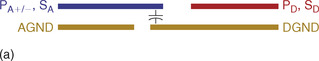
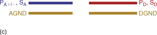
Split Power and Ground Planes
The solution to the problem of digital noise being injected into analog circuitry through the supply planes is to segregate the analog components from the digital ones and eliminate common return paths. Segregating the components is straightforward; the components are physically placed in different places on the board. Eliminating common return paths can be accomplished by splitting the ground and power planes into separate areas. The various planes are shown in Figure 6-15. A typical plane is one continuous sheet (an entire layer dedicated to a single power or ground connection) as shown in Figure 6-15(a). But it is possible and advantageous to break up the plane into sections or to create completely separate planes for the digital and analog areas. Figure 6-15(b) shows a split plane that provides isolated areas on a single layer while providing an electrically common reference point. This configuration is common where power electronics are placed over the plane area that is close to the board connectors, and analog and digital electronics are placed over their respective return planes. This allows all circuits on the board to be referenced to a common ground but forces the specific return currents to stay within their own areas. This is demonstrated in the PCB Design Examples.
 |
 |
 |
 |
| Figure 6-15 Different types of power/ground planes: (a) continuous plane; (b) split plane; (c) moated plane; (d) isolated, continuous planes. |
Return planes can also be completely separate areas by using moats as in Figure 6-15(c) or distinct continuous planes as shown in Figure 6-15(d). Moated planes are sometimes used as local ground or reference planes for high-speed clocks or small sections of a circuit that require their own regulated supply or ground potential, and isolated planes are used where parts of the system do not share a common ground reference or power supply system.
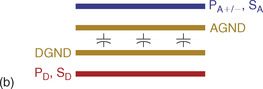
Care must be exercised when using split or multiple isolated ground and power planes. Even if the planes are separated physically, noise can be capacitively coupled from one plane to the next as shown in Figures 6-16(a) and 6-16(b). To minimize noise coupling between analog and digital planes, split planes on different layers should be prevented from overlapping each other, as shown in Figure 6-16(c), or should be separated with a shield plane, as shown in Figure 6-16(d). This is demonstrated in Example 3 in the PCB Design Examples.
 |
 |
 |
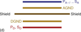 |
| Figure 6-16 Power and ground plane stack-up scenarios: (a) coupling between overlapped planes, (b) coupling between parallel planes, (c) nonoverlapping split planes, (d) shielded isolated planes. Key: P, power; S, signal; A, analog; D, digital. |
On rare occasions the analog and digital return or reference planes of a PCB may be on different layers (and not overlapping or separated by a shield plane) but must be referenced to a common point (for example, when working with analog-to-digital and digital-to-analog converters). So the question becomes how to keep them physically separated but electrically connected. The easiest way is by using the isolated planes (Figure 6-15(c)) and then connecting the planes at a point using a plated through hole as shown in Figure 6-17(a) or a shorting bar. Moated planes (Figure 6-15(c)) can also be connected using the shorting bar. Both of these methods can be used in PCB Editor and are demonstrated in the PCB Design Examples.
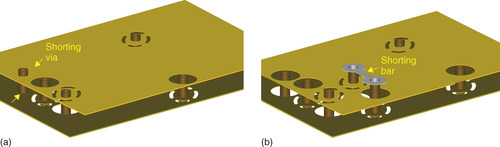 |
| Figure 6-17 Methods of shorting together separate plane layers: (a) a via as a short, (b) a copper trace (strip) as a short. |
PCB Electrical Characteristics
Characteristic Impedance
It was stated earlier that to minimize cross talk we want to minimize trace (loop) inductance and maximize the capacitance to the return plane. What does this do to the characteristic impedance,
Z0, of a trace?
Perhaps the first thing to do is to look at what characteristic impedance really is. For example RG58 is a coaxial cable that is often used as a shielded transmission line in 50-Ω systems. Actually, RG58 is about 52
Ω, not 50
Ω. But even so, what does that mean? If you use an ohmmeter to measure the resistance from the center conductor to the shield you will see that it is neither 52 nor 50
Ω. So how is its characteristic impedance 52
Ω?
Figure 6-18 shows a model of a transmission line, which consists of series inductors and parallel capacitors. This is called the
lumped-element model, which assumes that the series resistance is negligibly small and that the transmission line is infinitely long (or at least long enough to watch what happens). Each
LC“lump” represents a finite section of the transmission line, and the sum total of the elements is representative of the total inductance and capacitance of the transmission line.
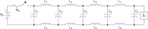 |
| Figure 6-18 A lumped-element transmission line model. |
We begin the analysis with all of the capacitors discharged and all currents at zero. At time
t = 0
s the switch is shut, which applies the source voltage,
VS, to the transmission line through the source resistance
R
s as shown in Figure 6-19. Initially
C1 acts as a short circuit so
I =
V
S/R
S. Current,
I, begins to charge capacitor
C1, and a return current will also flow out of the bottom of
C1 back to the source (note that this is a
displacement current as postulated by Maxwell rather than a
conduction current as defined by Ampere). The instantaneous impedance is
Z
C1=
Vline/
I.
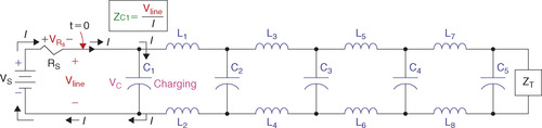 |
| Figure 6-19 A signal applied to the transmission line. |
As
C1 charges (no longer acting like a short), current begins to flow into
L1. Each inductor pair (
L1 and
L2,
L3 and
L4, etc.) is mutually coupled, so the magnetic field of
L1 induces the return current in
L2.
As current flows past
L1,
C2 begins charging positively on the top side; and as
L2 forces return current to flow back to the source (due to mutual inductance),
C2 begins charging negatively on the bottom side (relative to its top lead).
At some point
C1 becomes fully charged to a value of
V
C1 =
Vline =
V
S−
I×
RS and then the displacement current no longer flows through
C1, so the instantaneous impedance at
C1 is
Z
C1 = ∞ and
Z
C2 = V
line/
I. Current continues down the line, charging up each capacitor in turn to a value of
V
Cn =
Vline.
As each capacitor along the way is charging, the instantaneous impedance across the line is
Z
Cn =
Vline/I
Cn as shown in Figure 6-20. As each capacitor becomes fully charged, its impedance goes to infinity because the displacement current through it goes to zero. As seen from the source (
V
S) the impedance of the line is
Zline =
Vline/
I =
Vline/
I
Cn and is dynamic since it travels along the line. Furthermore, the impedance farther down the line is unknown.
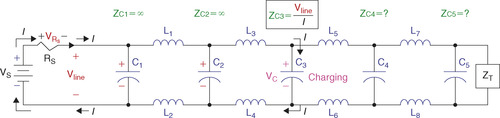 |
| Figure 6-20 The instantaneous impedance propagates along the transmission line. |
The speed at which the instantaneous impedance travels along the line is dependent on the inductance and the capacitance of each section. It was said above it is desirable to have as little loop inductance as possible (which will never be zero) and as much capacitance as possible (which will never be infinite). Thus there will always be finite inductive reactance (
X1) and capacitive reactance (
X
C) during any transient. However, the capacitors that are charged have nothing to do with the impedance (since they look like open circuits) and the inductors that have steady-state current flowing through them have nothing to do with the impedance (since they look like shorts). The capacitors and inductors farther down the line have nothing to do with the impedance either, since they do not see any action until the capacitors and inductors before them have approached a steady-state condition. Until the voltage (
Vline) reaches the load,
Z
T, the source actually has no idea the load,
Z
T, even exists; neither does it know how many sections of
L and
C there are until all of the previous sections have reached steady state. If the impedance of each section is the same all along the line, then we call the instantaneous impedance the characteristic impedance of the transmission line and give it the special symbol
Z0.
Before we consider what happens to the current flow and line voltage in Figure 6-20 once all of the capacitors are charged and the line voltage and current reach
Z
T, we need to take a closer look at the behavior of the transmission line. From the above discussion we see that it takes a finite amount of time for the applied voltage (minus the voltage drop,
V
Rs) to propagate down the line, and, as the applied voltage propagates, it essentially behaves as a wave. In fact the effects described here are due to wave properties and not directly due to electrons flowing (at least not like we normally think of them). The key to understanding
Z0 (and reflections and ringing, as we will see shortly) is in understanding how and at what speed the waves travel.
If you ask an average person how fast electricity travels, you will usually get the answer that it travels at the speed of light. Except in one particular case, that answer is not correct. If we think of electricity as flowing electrons, then electricity actually travels at only about 1
cm/s (Bogatin 2004, p. 211), pretty slow really. This seems counterintuitive since when we turn on a light switch the lights come on seemingly immediately, as if the “electricity” traveled at the speed of light from the switch to the light bulb. But what does travel at (almost) the speed of light is the electromagnetic wave that is launched into the wiring by the switch closing.
Figure 6-21 can be used to explain the difference between the speed of electrons and the electromagnetic wave velocity. The figure shows a copper tube, which contains marbles that are separated by small springs. If an additional marble (No. 5) is shoved into the tube, marble 4 is shoved further into the tube, compressing the spring between it and marble 3. Note that in this early stage marbles 2 and 1 have no idea what is going on yet. As No. 5 is shoved into No. 4’s place the rest of the marbles must “do the wave” to make room for it. Eventually all of the marbles have slid over by one marble space and marble 1 pops out the other end.
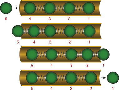 |
| Figure 6-21 Wave velocity vs. particle velocity. |
Notice now that all of the marbles have moved a distance of only one marble space, but the effect of this movement (a wave) is felt at the end of the tube in about the same amount of time. The speed of the wave is determined for the most part by the value of the spring constants and partly by the momentum of the marbles.
So in a transmission line the electrons travel slowly, but the electromagnetic (EM) waves travel fast. The speed of the EM wave is determined by how quickly the magnetic fields in the inductors and the electric fields in the capacitors can be built up or dissipated, which is influenced by the material properties and geometry of the PCB through which the wave travels.
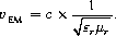
The velocity of an EM wave through a medium is described by Eq. (6.10),
 where
vEM is the velocity of the EM wave in a given material, ε
0 is the permittivity of free space (8.89×10
−12 F/m), ε
r is the relative permittivity (dielectric constant) of the material (a unitless constant relative to ε
0), μ
0 is the permeability of free space
(4Π×10
−7 H/m), and μ
r is the relative permeability of the material (a unitless constant relative to μ
0).
where
vEM is the velocity of the EM wave in a given material, ε
0 is the permittivity of free space (8.89×10
−12 F/m), ε
r is the relative permittivity (dielectric constant) of the material (a unitless constant relative to ε
0), μ
0 is the permeability of free space
(4Π×10
−7 H/m), and μ
r is the relative permeability of the material (a unitless constant relative to μ
0).
(6.10)
You may recall that the speed of light,
c (a special EM wave), in free space is

(6.11)
So we can rewrite Eq. (6.10) as
(6.12)
As stated, the terms ε
r (relative permittivity) and μ
r (relative permeability) are unitless. Furthermore μ
r is equal to 1 in free space and in most polymers (including FR4 laminate), so we can further simplify Eq. (6.12) as shown in Eq. (6.13):

(6.13)
From Eq. (6.13) we see that the velocity of an EM wave (which comprises both electric and magnetic fields) in a PCB varies inversely with the relative permittivity, ε
r.
Relating this observation with Eq. (6.7), we can state (without rigorous proof) that the capacitance of a transmission line is determined by the geometry of the transmission line and the relative dielectric constant (ε
r) within the transmission line. And the inductance of a transmission line (specifically the loop inductance) is determined by the geometry, but μ
r falls out since it is equal to 1 (see Eq. [6.5] and Figure 6-4 and Figure 6-5).
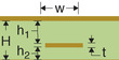
In practice, calculating the characteristic impedance, capacitance, and inductance can be fairly complex, depending on the geometry of the circuit, but fortunately that has been done for us for the most common transmission line configurations. The equations are shown in Table 6-2Table 6-3Table 6-4 and Table 6-5. The PCB designer has full control over the trace width (
w) and partial control over the trace thickness (
t) by selecting the ounces per square foot but may have little or no control over the thickness of the laminate (
h). These equations are solved for
w and presented later in this chapter (in Table 6-6 and Table 6-7).
| Microstrip transmission lines | Characteristics | Intrinsic propagation delay | |
|---|---|---|---|
| Surface | Topology | Characteristic impedance | |
 | |||
| k=87 for 15< w<25 mils [1][2][3] and [4] | |||
| k=79 for 5< w<15 mils [3] and [4] | |||
| Restrictions | |||
| 0.1< w/ h<3.0 [1] | |||
| 1<ε r<15 [1] | |||
| Design equations | |||
| Trace routing width to use in PCB Editor | |||
| (use k=87, then check against width rules, use k=79 if necessary) | |||
| Surface differential | Topology | Characteristic impedance | |
 | |||
| (same as surface microstrip) [5][6] and [7] | |||
| Differential impedance | |||
| Restrictions | |||
| None specifically noted except as applies to the surface microstrip. | |||
| Design equations | |||
| Trace routing width to use in PCB Editor | |||
| Trace separation: | |||
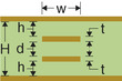
| Embedded | Topology | Characteristic impedance | |
where
 | |||
| OR | |||
| [1] | |||
| Restrictions[8] and [10] | |||
| 0.1< wlh2<3.0 | |||
| 1<ε r<15 | |||
| Line widths: 0.127(5 mils) to 0.381
mm (15 mils)
Dielectric thickness: 0.127 (5 mils) to 0.381 mm (15 mils)40< Z0<90 Ω | |||
| Design equations | |||
| Trace routing width to use in PCB Editor | |||
| w=7.475 h 2×e −x−1.25 t | |||
| where | |||
| OR | |||
 | |||
| Embedded differential | Topology | Characteristic impedance | |
| Differential impedance | |||
 | |||
| Restrictions[5] | |||
| Same as embedded microstrip | |||
| Design equations | |||
| Trace routing width to use in PCB Editor | |||
| w=7.475 h2×e −x−1.25 t | |||
| where | |||
 [1] [1] | |||
| Trace separation of pair: | |||
| Stripline transmission lines | Characteristics | Intrinsic propagation delay | |
|---|---|---|---|
| Balanced (symmetric) | Topology | Characteristic impedance | |
 | Restrictions Line widths: 0.127 (5 mils) to 0.381 mm (15 mils)Dielectric thickness: 0.127 (5 mils) to 0.381 mm (15 mils) 40< Z0<90 Ω Design equation | ||
| Trace routing width in PCB Editor: | |||
 | |||
| Unbalanced (asymmetric) | Topology | Characteristic impedance | |
 | |||
| Restrictions | |||
| Design equation | |||
| Trace routing width in PCB Editor | |||
| w=2.375(2h 2 + t) e−x−1.25 t | |||
| where | |||
 | |||
| Stripline transmission lines | Required trace width (in) for desiredZ0 and/orZdiff. | Intrinsic propagation delay | |
| Broadside coupled differential stripline (symmetric)[12] | Topology | Characteristic (between conductors) impedance | |
 | Restrictions None given in the references Design equations Trace routing width to use in PCB Editor w=7.475 d×e −x−1.25 t where | ||
| Edge coupled differential stripline (symmetric)[12] | Topology | Characteristic impedance | |
| For symmetric ( h1= h2) or asymmetric ( h1 ≠ h 2) | 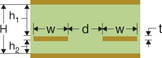 | For symmetric ( h1=h 2) | |
| For asymmetric (h 1≠ h2) | |||
| Differential impedance (both) | |||
| Design equations | |||
| Trace routing width to use in PCB Editor | |||
| For symmetric (h 1=h 2) | |||
 | |||
| For asymmetric ( h1≠ h2) | |||
| w=2.375(2 h2 + t)×e −x−1.25 t | |||
| where | |||
 | |||
| Trace separation in layer stack-up (for symmetric or asymmetric) | |||
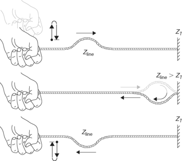
Reflections
So the next question is, What happens when the voltage “wave front,”
Vline, reaches the termination impedance,
Z
T? The answer is that it depends on what
Z
T is.
Let’s assume for a minute that
Z
T is an open circuit. When the last capacitor,
C5, in Figure 6-18 is charged and
Vline reaches
Z
T (which equals infinity), then all capacitors are charged along the line (and their impedance equals infinity), so all current stops—or at least it would like to. But it cannot, because all of the inductors have current,
Iline, through them and they will not allow
Iline to stop instantly. As the magnetic fields of
L7 and
L8 begin to collapse to try to maintain their current (remember that they are mutually coupled and influence each other), they continue to shove current into
C5, raising its voltage a bit more (we will see later what
a bit more means).
The magnetic fields of each inductor pair (
L3 and
L4,
L1 and
L2, etc.) will collapse, one after the next, back toward the source and raise the voltage of its nearest capacitor, all the way down the line. This new voltage front (
Vline + a bit more) propagates back from
Z
T toward the source with the collapsing magnetic fields until all of the magnetic fields have collapsed and all of the capacitors have this new charge on them. An analogy of a reflection from a high impedance termination is shown in Figure 6-22, which shows a person launching a wave into a rope. If the rope experiences little or no friction, the wave will propagate down the rope unattenuated. If the end of the rope is loose (a high impedance), the wave will be reflected back toward the person, who will feel an identical wave returned.
 |
| Figure 6-22 Positively reflected wave (
Z
T is an open circuit). |
In the example above the reflected wave has the same polarity and amplitude of the transmitted (incident) wave. In reality the rope would not be in a frictionless environment (and
Z
T would not be infinitely high). In that case the reflected wave would still have the same polarity as the incident wave but the amplitude would be less.
The magnitude and polarity of the reflected wave are described by the reflection coefficient, ρ (Greek letter
r), as shown in Eq. (6.14):

(6.14)
The reflection coefficient can have values between −1 and +1. If
Z
T>
Zline (i.e., as
Z
T approaches ∞
, as in the example above), then
 which means that the reflected wave will be exactly the same amplitude and have the same polarity as the incident wave.
Next we consider what happens if
Z
T (in Figure 6-18) is a short circuit instead of an open circuit. At first the exact same thing occurs as described above when the switch is shut. That is (assuming the same initial conditions as above, all caps are discharged, etc.), the capacitors and inductors take their turn charging up and building up magnetic fields,
Vline is applied to the line, current
Iline. flows, and
Z
Cn =
Vline/
I
Cn. So the instantaneous line impedance is equivalent to
Z
Cn. A different result occurs at the end of the transmission line. Since
Z
T = 0
Ω and inductors
L7 and
L8 again want to maintain their current flow,
Iline flows straight through the short, Z
T.
Since the current through
L7 and
L8 is maintained (even for just an instant) and since the voltage drop across an inductor with a constant current flow is zero, capacitor
C4 sees the short and begins to discharge through
L7 and
L8 (helping to maintain their current flow) and on through the short,
Z
T. A short moment later
C4 is at the same potential as
C5 and
Z
T (0
V), while
L7 and
L8 have managed to maintain their current. The capacitors continue to discharge one after the other (
C3 then
C2, etc.) and each inductor pair maintains its current until finally all capacitors are shorted (and all the inductors look like a short if they have the same constant current). In the final analysis,
Vline =
V
ZT = 0
V and therefore
Zline = 0/
Iline = 0
Ω and
Iline =
V
s/
R
s.
A mechanical analogy of a wave reflected negatively from a “dead short” is shown in Figure 6-23. If a positive wave is launched into a rope that is rigidly fixed at the end, the wave will be negatively reflected. In a perfectly lossless environment, the reflected wave will be of the same magnitude but opposite polarity as the incident wave.
 |
| Figure 6-23 Negatively reflected wave (
Z
T is a short circuit). |
In the electrical example above, the negatively reflected wave has the same magnitude as but opposite polarity to the voltage stored on the capacitors. As the negative wave hits each capacitor, it is forced to give up its charge (as current), which helps maintain the current flow through the nearest inductors and all the way down the line through the short at the end of the line. This negatively reflected wave is again represented mathematically by the reflection coefficient (Eq. [6.14]), but in this case since Z
T<
Zline (i.e., as Z
T approaches 0), ρ = −1, as shown in Eq. (6.15):

(6.15)
Now let’s say for argument that the characteristics of our transmission line are such that when we calculate
Z
Cn =
Vline/
I
Cn at each capacitor/inductor section, Z
Cn = 50
Ω. Let us also set
R
s = to 50
Ω. Now what happens when
Z
T = 50
Ω? As you can suppose by this time, at the moment the switch is shut, the capacitors take their turn getting charged (and the inductors are building their fields). Since each
Z
Cn = 50
Ω, then
Zline is also 50
Ω. Since
R
s and
Zline are equal (and act as a voltage divider),
Vline = 1⁄2
V
s. Once the wave front has propagated down the line and reaches
Z
T, which is also 50
Ω,
Iline continues to flow into
Z
T as if nothing different has occurred and
V
ZT =
Vline = 1⁄2
V
s. As long as Z
T is purely resistive, then everything is at steady state and
Zline =
Z
T = 50
Ω. Also no voltage is reflected back toward the source because no change in voltage occurred on the capacitors and no current change occurred in the inductors.
In this case, since
Z
T =
Zline the reflection coefficient is 0 (ρ = 0) as shown in Eq. (6.16):
(6.16)
The mechanical analogy is shown in Figure 6-24, in which none of the wave energy is reflected but is perfectly absorbed into the load at the end of the line.
 |
| Figure 6-24 No reflection (
Z
T absorbs wave energy). |
From these examples we can conclude that
Zline is in effect only during voltage transitions and is the result of the voltage and the current transients that flow to charge the line capacitance to the new voltage and to build the magnetic fields in the inductors. We can also see that, if the impedance
Z
T is not the same as
Z0, then a reflection will occur, but if the impedance
Z
T is the same as
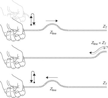
Z0, then no reflection will occur. Furthermore it takes a finite amount of time for a wave front to propagate from one end of a transmission line to the other, and if a reflection does occur it takes another finite amount of time for the reflection to propagate back to the source. What happens at the source is the next topic.
Ringing
When ρ ≠ 0 between any adjacent impedances, reflections will occur. This is true both from driver to transmission line and from transmission line to load (and back). If there is little or no loss along the transmission line, the reflected waves will bounce back and forth between the driver and the load if they are not matched to the transmission line (or if the transmission line is not matched to them). When viewing a particular point along the path, for example at the output pin of a gate or amplifier, the repeated reflections will be evident as ringing. Ringing is a direct result of reflections, which in turn are due to impedance mismatches.
One of the problems with ringing is that the voltage at any point along the line is effectively out of control, since ringing causes voltage overshoots and undershoots (see Figure 6-26 later). Overshoots can actually damage active devices that have input voltage limitations and will radiate greater EMI than normal signals. Overshoots and undershoots can cause digital circuits to be falsely triggered if the reflected voltage swings across switching thresholds. In analog circuits the interactions between a continuous wave signal and its reflections creates standing and/or traveling waves that can degrade the signal of interest.
The magnitude and frequency of the ringing depend on the speed of the wave through the transmission line, the length of the line, and the reflection coefficient at each impedance discontinuity. We take a detailed look at ringing using the circuit shown in Figure 6-25.
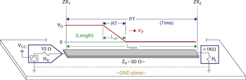 |
| Figure 6-25 Representation of signal propagation on a PCB trace. |
The circuit consists of a driver that is powered by
VCC and has a low output impedance,
R
S (10
Ω); a transmission line with a characteristic impedance,
Z0 (50
Ω); and a receiver with a high input impedance,
R
L (usually 1
kΩ or higher). The dashed lines indicate the interfaces of the mismatched impedances and are labeled as ZX
1, and ZX
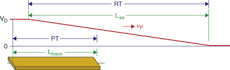
2. The dimensions in green represent length, and the dimensions in blue represent time. The circuit in the figure can be used to represent an analog or digital circuit, but we will consider the digital application.
Consider the following:
▪ RT is the rise time, the time it takes for the output of a driver to transition from a minimum value to a maximum value. RT is specific to individual devices and is given in the data sheets.
▪
Ltrace is the length of a trace (transmission line) on the PCB.
▪
v
P is the propagation velocity of a wave and is determined by
Z0 which is determined by ε
r and the transmission line dimensions (trace width and distance to the ground plane).
• PT is the propagation time, the time it takes for the transition to propagate from one end of the transmission line to the other.
▪
LSE is the effective length of the rising edge (also called
transition distance or the
spatial extent of the transition [Bogatin 2004, p. 215] or
edge length [Johnson and Graham 1993, p. 7]).
▪ Length and time are related by the propagation velocity of the wave,
v
p (units of distance/time), where PT =
Ltrace/
v
p (units of time) and
LSE =
v
P× RT (units in distance).
• If length of the trace,
Ltrace, is longer than the spatial extent of the rising edge,
LSE, then the rising edge will fit entirely within the length of the trace and the reflection voltage will be an amplitude-scaled copy of the entire rising edge, for which the scaling is determined by the reflection coefficient, ρ. Another way of looking at the same thing is if the RT (rise time) is faster than the PT (propagation time), then the rising edge will have time to be fully reflected.
Electrically Long Traces
The goal is to design PCB traces such that they do not allow conditions to exist under which propagation times are too slow (compared to signal RTs) or a trace’s length is too long (compared to a signal’s spatial extent). When these conditions cannot be met, the trace is considered to be “electrically long” and must be treated as a transmission line. Proper treatment of a transmission line means controlling the impedance of the line over the entire length of the line and matching the impedance of the line with the source and load impedances so that reflections do not occur.
The obvious question is, when is a trace too long (or when is the RT too fast)? The magnitude of reflections and the ringing frequency are governed by the down and back (round trip) time of the reflections. Much of the literature states that the propagation time, PT, should be less than one half of the rise time (i.e., PT <½RT) or that the length of the trace should be less than one half of the special extent of a rising edge (i.e.,
Ltrace < ½
LSE). These relationships define the limits, not the goal. The shorter trace lengths are or the slower the RT is, the better off you will be. The examples below illustrate this in greater detail. After the examples general design recommendations are provided.
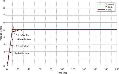
Figure 6-26 shows what happens when PT is too long compared to RT. The data in the figure were generated using the transmission line model found in PSpice and the PT was set four times longer than the RT (instead of being<1⁄2RT).Refer to Figure 6-25 and Figure 6-26 during the discussion.
0. At time
t = 0
ns the logic gate output (
Vsource) switches to
VCC = 5 V
DC and begins to increase in voltage at the output (
Vdrive) (start of rising edge). The first capacitor in the transmission line is uncharged and acts like a short to GND.
1. At
t = 10
ns the gate has finished switching and the voltage at the output of the driver,
V
D, is
 because of the voltage divider established by
R
s and
Z0. At this point the beginning of the rising edge is halfway to the load, and the tail end of the rising edge is just leaving the load side of
R
s.
because of the voltage divider established by
R
s and
Z0. At this point the beginning of the rising edge is halfway to the load, and the tail end of the rising edge is just leaving the load side of
R
s.
2. At
t = 20
ns the beginning of the rising edge reaches the load resistor,
R
L. Since there is an impedance mismatch between
Z0 (50
Ω) and
R
L (1
kΩ), there is a positive reflection that begins immediately to head back to
R
S. The reflected voltage is added to the rest of the rising edge as it continues to arrive at
R
L. The reflection coefficient looking into the load from the transmission line is ρ = (1000−50)/(1000 + 50) = 0.90.
3. By
t = 30
ns the trailing end of the rising edge reaches the load. The voltage at the load (
Vload) is now the sum of its previous voltage (0
V) plus the value of the incoming voltage (4.17
V) plus the reflected voltage (4.17×0.90 = 3.75
V) for a total of 4.17 + 3.75 = 7.92
V. The reflected voltage (3.75
V) is well on its way back toward the source.
4. At
t = 40
ns the rising edge that was positively reflected from the load begins to arrive at the source,
R
S. The voltage at the source begins to rise (pts 4 to 5). However, since the impedance of the transmission line is greater than that of the source resistor, a negative reflection immediately begins to head back to the load. The reflection coefficient from the transmission line looking into
R
S is
5. At
t = 50
ns the 3.75
V reflected off from the load has completely reached
R
s. The voltage at the load side of
R
s is the sum of its original value (4.17
V) and the incoming reflected voltage (3.75
V) plus the voltage being rereflected back to the load (−0.667×3.75
V = −2.50
V) for a total of 4.17 + 3.75 + −2.5 = 5.42
V. And the −2.50
V is on its way to the load.
6. At
t = 60
ns the −2.50
V reaches the load and begins to lower the load voltage from its previous value of 7.92
V. Because of the impedance mismatch between the transmission line and the load, a reflection is immediately launched again. The reflection coefficient is still + 0.90, so the reflection will have the same polarity as the incident wave. Since the incident wave is the −2.50
V reflected off from
R
S, the load will reflect back a negative voltage. As the incoming −2.50
V runs into a positively reflected negative voltage, the overall voltage at the load (pts 6 to 7) drops significantly since ρ is high (0.90).
7. At
t = 70
ns the −2.50
V reflected off from the source has completely reached
R
L where the voltage is the sum of its original value (7.92
V) and the incoming reflected voltage (−2.50
V) plus the voltage being rereflected back to the load (−2.50
V×0.90 = −2.25
V) for a total of 7.92 + −2.50 + −2.25 = 3.16
V). And of course the −2.25
V is on its way to the source.
8. At
t = 80
ns the negative voltage that was reflected (positively, i.e., leaving the sign intact) from the load begins to arrive at
R
s. Since the incoming voltage is negative, the voltage at
R
s begins to fall. But since there is still a negative reflection coefficient (−0.667) from the transmission line looking into
R
s, the wave that immediately begins to bounce off from
R
S is now positive and heads back to the load.
9. At
t = 90
ns the −2.25
V reflected off from the load has completely reached
R
s. Again the voltage at
R
s is the sum of its previous value (5.42
V) and the incoming reflected voltage (−2.25
V) plus the voltage being rereflected back to the load (−0.667×−2.25
V = + 1.50
V) for a total of 5.42 + −2.25 + 1.50 = 4.67
V). And of course the + 1.50
V is on its way to the load.
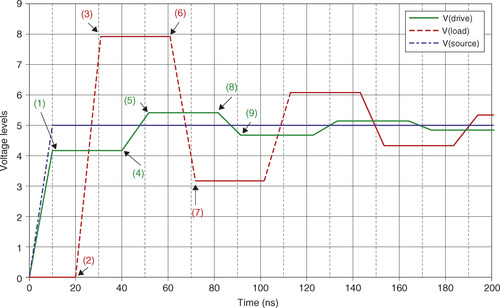 |
| Figure 6-26 Ringing on an electrically long transmission line. |
The reflections continue back and forth but decrease in value each trip. The losses occur because the energy that is not reflected at each impedance interface is absorbed into the source and load resistors. Eventually, the reflections become too small to notice and we say that it has reached steady state. The time to reach steady state is called the
settling time and the shorter the settling time, the better.
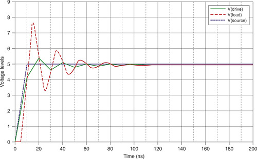
If the length of the trace,
Ltrace, is much shorter than the special extent of
LSE (as represented in Figure 6-27), then the rising edge will not fit within the length of the trace and will reach the driver before the driver has even completely reached is steady-state value. If the trace is very short, the reflection voltage will be reflected many times and repeatedly fold back onto itself as the driver output climbs to its steady-state value. Since the voltage at an interface is the sum of its existing voltage, the incoming reflection, and the reflected reflection, the effects of the reflections become “smeared” into each other. By the time the driver has fully reached its final value most of the reflections have come and gone and only the last, smaller overshoots and undershoots are evident.
 |
| Figure 6-27 Representation of an electrically short trace. |
Figure 6-28 shows what happens when PT is much shorter than RT on an electrically short trace. The reflections occur as previously described, but as shown in the graph many of the reflections have occurred by the time the driver reaches its full output level. Recall that the voltage at each impedance interface is the sum of its previous voltage plus the incoming voltage plus the reflected voltage, but since the reflections happen fast (relative to the rise time), each reflection never has a chance to reach its full voltage level (only a fraction of the rising edge at that time), so the reflections are much smaller and therefore the peaks (overshoots) and valleys (undershoots) are also much smaller (hardly noticeable), while the driver output is still rising. Also the ring frequency is higher with the shorter trace.
 |
| Figure 6-28 Negligible ringing on electrically short traces. |
Critical Length
As mentioned above an electrically short trace is one for which the propagation time is less than one half of the rise time (i.e., PT<1⁄2RT) or the length of the trace is less than one half of the special extent of a rising edge (i.e.,
Ltrace < ½
LSE). The length of a trace or transmission line for which these conditions are just barely met is called the
critical length. Figure 6-29 shows the voltage levels at critical length. Ringing still occurs, but the peaks never level off and the reflections settle sooner. But again the one-half rule is a limit and not a goal. Examples of determining critical length and designing transmission lines are given in the design section below and in Example 4 in the PCB Design Examples.
 |
| Figure 6-29 Reflections when PT = ½RT. |
Transmission Line Terminations
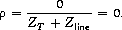
If we cannot make the rise time slower and/or the length of the trace shorter, then we will have noticeable reflections and ringing. The only other way to stop the reflections and ringing is to eliminate the impedance mismatches that are causing them by properly terminating the ends of the transmission line with the proper source and/or load resistors.
We can make
R
s = Z
0 =
R
L by using a resistor in series with the source and a resistor in parallel with the load.
If the impedances are all matched then there will be no reflections, as shown in Figure 6-30. However, only half the voltage will reach the load because a voltage divider results with
R
S equal to
R
L so
Vload = 1⁄2
Vsource. This lower voltage at the load may not reach required logic thresholds, preventing affected digital circuits from functioning.
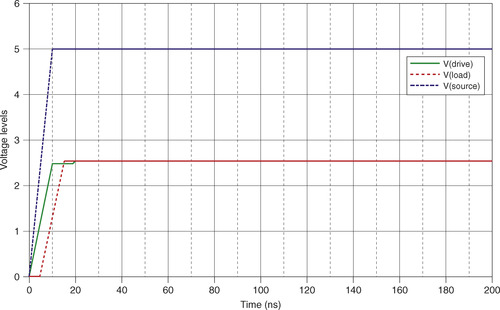 |
| Figure 6-30 No reflections when all impedances are matched. |
An alternative is to put a resistor in series with the driver such that the impedance that the transmission line sees looking at the driver and series resistor is equal to
Z0. So if
Z0 is 50
Ω and the driver output resistance is 10
Ω, then the transmission line will be matched to the driver by putting a 40-Ω resistor in series with
R
s. An example of the result is shown in Figure 6-31. Even when PT is >1⁄2RT, only one reflection occurs (the fiat section on
Vdrive between 10 and 20
ns) and it is absorbed into the 40-Ω resistor and
R
s, so the reflection dies there. An advantage of this type of termination technique is that the voltage at the load is also much closer to the ideal voltage. The momentary hold on
Vdrive is usually not a problem, but it can be a problem in high-speed clock circuits for which the steady-state on (off) time is about the same duration as the rise time.
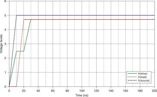 |
| Figure 6-31 Reducing reflections by using a resistor in series with the source. |
PCB Routing Topics
There are four areas for electrical considerations when routing your PCB: placing parts, PCB layer stack-up, bypass capacitors, and trace width and spacing width.
Parts Placement for Electrical Considerations
Chapter 5 addressed parts placement with manufacturability in mind. Here we consider parts placement with electrical performance in mind. Usually the two goals complement each other, but occasionally they conflict. When conflicts do occur an attempt should be made to resolve the conflict in a way that is mutually beneficial. If that is not possible, electrical considerations usually have priority over mechanical considerations unless doing so will result in a mechanical failure of the board. For example, it may be necessary to manipulate the assembly or soldering processes or place parts on both sides of the board in order to meet manufacturability requirements and meet electrical performance requirements. Whatever solution is chosen the PCB needs to be manufacturable and operational.
Aside from manufacturability goals the first approach to placing parts for electrical considerations is usually determined by the function of the circuit. This is especially true for analog circuits where a signal enters the PCB, flows through the circuitry in more or less a single path (including feedback networks), and then leaves the board. Since analog circuits are susceptible to noise the goal is usually to place the parts to minimize the possibility of degrading the signals. This usually means keeping the parts as close together as possible so that the traces can be as short as possible and keeping the signal path as straight as possible (not zigzagging back and forth or from one side of the board to the other). This approach may increase the size of the board, however, and is not always possible.
With digital circuits it is also desirable to keep related parts close together and lines short, but because digital circuits often contain many parallel paths and branches and may contain wide data busses it may be nearly impossible to do so. Sometimes the best that can be accomplished is to keep parts that are functionally related closer together or place parts together that have the highest speed clocks and rising edges in order to minimize the length of related signal lines.
Mixed signal boards are even more challenging, in that both analog and digital circuits and high-power circuits (such as switching regulators) exist on the same board. In these cases the PCB should be segregated into different areas as shown in Figure 6-32. The topology may vary but the idea is to keep the higher power and other noisy circuitry closer to the connector if possible. This limits the amount of return plane that is utilized by these circuits and therefore minimizes the amount of return plane that is common between them and the rest of the circuitry. Digital and analog circuits should also be kept apart from each other to minimize the effects of switching noise on analog circuitry. When dividing the PCB in this way, it is usually necessary (and beneficial) to set up split and isolated plane layers as shown in Figure 6-15.
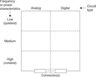 |
| Figure 6-32 Board layout recommendations for noisy circuits. |
PCB Layer Stack-Up
Although PCB Editor’s
Layout Cross Section dialog box allows you to define a stack-up, the PCB layer stack-up and thicknesses are really assigned when the board is ordered from the manufacturer. But the PCB layer stack-up and thickness need to be defined early in the design stage before working in PCB Editor, since the stack-up will determine how many layers to enable and how many power and ground planes to establish. The strategy for stacking up a PCB depends on a number of things such as the capabilities of your board manufacturer, the circuit density (both routing and parts), the frequency (analog) and rise/fall times (digital) of the signals, and the acceptable cost of the board.
As circuits become more dense, additional routing and plane layers are required.Digital circuits commonly require more layers than analog circuits because digital circuits typically consist of parts with greater numbers of pins per chip and because they have a higher number of parallel interconnections. High-speed circuits (whether analog or digital) may require a greater number of layers even if they are not very dense. This is because multilayer boards can provide better impedance control and shielding since they can have additional ground planes. The more layers a board has, the more it costs, but once a PCB stack-up exceeds four layers, the cost increase per layer usually becomes less for additional layers (to a point). Additionally the benefits of shielding and impedance control can considerably outweigh the increased cost of extra layers.
There are many possible ways to design the stack-up. If the board will be operated at low speeds and in an isolated environment almost anything you can dream up will work. However, as signal speeds increase the layer stack-up and trace routing become increasingly important because a poorly designed stack-up can lead to reflections and excessive EMI radiation (affecting external circuits as well as causing self-inflicted cross talk). A well-designed layer stack-up (and proper routing) not only minimizes the energy it radiates, but also can make your circuit relatively immune from external sources of radiation. In designing a layer stack-up there are only a few guidelines to follow, but they are important. The following few paragraphs and the examples demonstrate the guidelines.
Since PCBs are constructed of double-sided cores bonded together with prepreg, multilayer PCBs usually contain an even number of layers. Odd-layered boards can be made, but in most cases there is no cost benefit to adding only one layer instead of a layer pair (e.g., if you need five layers you may as well go with six). The extra layer can be an extra return/ground plane and the symmetry of an even number of layers helps minimize board warpage.
A signal layer should always be adjacent (and close) to a plane layer (preferably a return/GND plane) to minimize loop inductance, which minimizes electromagnetic radiation and cross talk. Power planes should also be adjacent (and close) to a return plane as this adds interplane capacitance, which helps minimize power supply noise and radiation. If you have to choose between a signal layer being adjacent to the return plane and a power plane being adjacent to the return plane, choose the signal layer. You can add more bypass and bulk capacitors between the power planes to make up for the loss in interplane capacitance.
The following stack-up examples are offered as a reference only. There are many more combinations possible, but only a few are shown here (please see the references for additional examples and details). The final board thickness in the examples is 0.093 in. and the copper is 1
oz (1.35 mils) thick. The availability of certain dimensions will depend on the manufacturer’s capabilities and specific processes.
The thicknesses listed in the figures are given to provide perspective. You can use Table 6-3Table 6-4 and Table 6-5 to get an idea of the different combinations of cores and prepreg types used to make up different layer thicknesses, but remember that the thicknesses from the tables are preassembly thicknesses, and finished thicknesses may vary since traces sink into the soft prepreg, while plane layers do not (see the Advanced Circuits Web site, www.4pcb.com, for examples of layer thicknesses).
A signal’s return current will be on the ground or power plane that is closest to the signal line (if possible), and the relative dimensions determine the trace/plane routing pairs. Ideally all return currents will need to end up at the ground/return pin on the PCB’s power connector. It may be beneficial to stack up and route your PCB to
try to make it easier for the return currents of critical high-speed traces to be paired up with certain ground planes (so that they are not forced to go through capacitor leads or vias to get back to the ultimate return point), but there is no guarantee they will follow it. But remember that to an AC signal there is no real difference between the power plane and the ground plane because they are shorted together with bulk and bypass capacitors. So when signal traces transition from one layer to another, the return currents may not have an easy path from one ground plane to another and may choose to return to the source on a power plane until they find a convenient path back to the preferred ground plane through a bypass capacitor. While the return current is not flowing on the preferred plane, the impedance of a transmission line can be significantly different from what is expected. To assist the return current in staying with the signal line when it changes layers, return current bridges can be installed by using free vias connected to the ground planes or capacitors with fan-out vias near vias used to transition signals from one layer to another.
There are several symbols that need to be defined with regard to the stack-up figures. The
H in the figures implies horizontal routing and the
V implies vertical routing. In some of the figures, an
R is used to imply nonspecific routing direction. Concentrating the routing strategies in horizontal or vertical directions makes the routing process more efficient in high-density designs and reduces the number of vias required to complete the connections. The symbol HS is used to imply high-speed signals that are usually buried between plane layers for extra shielding. The GND symbol is used to represent any ground or return plane (for signal or power). The symbols PWR or ±PWR represent any power plane, such as + 5
V
VCC for digital circuits or +
V and −
V for analog circuits.
There are three basic types of transmission lines: microstrip, stripline, and coplanar. You may not always need a transmission line, but no matter how you route your board one of these types will be represented (even if it is not a close resemblance). Other types of transmission line configurations can be realized by other types of stack-ups, which are not shown here as they will depend on the capabilities and processes of your board manufacturer.
Figure 6-33 shows three different four-layer stack-ups. Indicated thickness is in mils.
 |
| Figure 6-33 Typical four-layer stack-ups. |
Figure 6-33(a) is one of the most common four-layer stack-ups for simple digital or analog PCBs. The land patterns and traces are placed on the outside (top and bottom) of the board and the power and return planes are inside. Placing the traces on the outside enables postfabrication inspection and troubleshooting.
Figures 6-33(b) and 6-33(c) place the power and return planes on the outside of the board and the traces on the inside. This arrangement helps shield the traces from outside EMI and helps contain self-generated radiation between the planes and consequently minimizes radiated EMI. The configuration in Fig. 6-33(c) can be used to route low-density analog circuits that require + /−
V for dual-supply op amps. Power is routed to the amplifiers with wide traces or copper pours and shares the layers used for routing signals.
Figure 6-34 shows examples of six-layer PCB stack-ups. Figure 6-34(a) is a typical stack-up for digital circuits or analog circuits that do not require dual-power supplies. This arrangement provides four routing layers and two plane layers. The inner routing layers can be used for the higher speed signals since they are shielded by the ground and power planes. For analog circuits that require dual power planes, the stack-up in Figure 6-34(b) provides a highly functional stack-up with two full routing layers, two partial routing layers (which share layers with the + PWR and −PWR layers), and ground planes that are adjacent to all signal and power layers and provide shielding for the inner signal traces. Alternatively the shared power and routing layers can be dedicated to power only, but this limits the board to two routing layers. The stack-up in Figure 6-34(c) provides two well-shielded, balanced stripline routing layers for high-speed digital circuits and adjacent ground planes for each of the signal and power layers. A limitation of this stack-up is that there are only two routing layers.
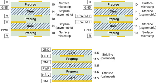 |
| Figure 6-34 Six-layer stack-up examples. |
Figure 6-35 and Figure 6-36 show examples of 8- and 10-layer stack-ups, respectively. Only a few examples are shown, but by using the different stack-up strategies of the previous examples and capitalizing on the various finished board thicknesses available from most board manufacturers, it can be seen that the higher layer stack-ups can provide a multitude of routing possibilities.
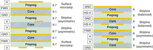 |
| Figure 6-35 Examples of eight-layer PCB stack-ups. |
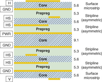 |
| Figure 6-36 A 10-layer PCB stack-up. |
Bypass Capacitors and Fan-Out
Bypass Capacitors serve two main functions, namely to short high-frequency noise to ground and to act as current reservoirs. Consequently there are three basic methods to fan out power pins. The first method usually occurs when the autorouter is used to create the fan-outs automatically. The autorouter creates individual fan-out vias for the IC’s power and ground pins, and it creates individual fan-out vias for each pin on the bypass capacitor (resulting in no direct trace connection between the IC and its capacitor). In general this is acceptable. The second method is to deliberately route the power pin to the bypass capacitor before the fan-out via and to the power plane as Figure 6-37(a) shows, and the third method is to route the power pin to the power plane first by placing the fan-out via between the power pin and the bypass capacitor as shown in Figure 6-37(b).
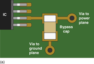 |
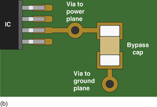 |
| Figure 6-37 Power pin fan-out methodologies: (a) power pin to bypass capacitor to via, (b) power pin to via to bypass capacitor. |
At first glance there may appear to be no difference electrically speaking, but the differences can be significant at high frequencies and fast rise times. Additionally, other issues such as the method of assembly (wave vs. reflow soldering) and the available board real estate often influence orientation and routing of bypass capacitors. Sources in the literature do not all agree with which method is best, but more often Figure 6-37(a) is recommended for analog circuits and Figure 6-37(b) for digital circuits.
Trace Width for Current-Carrying Capability
When current flows through a conductor, it will heat up due to
I2R losses. Wider traces exhibit less resistance and therefore less heating.
To determine the minimum trace width required to minimize heating, determine the maximum current a trace will carry and the thickness of the copper you will use on your board. Use Eq. (6.17) to calculate the minimum trace width,
 where
w is the minimum trace width (in mils),
h is the thickness of the copper cladding (in oz/ft
2),
I is the current load of the trace (in A),
k = 0.024 is used for inner layers and
k = 0.048 is used for outer (top or bottom) layers, and Δ
T is the maximum permissible rise in temp (°C) of the conductor above ambient temperature. You can also use the graph shown in Figure 6-38, which was derived from curves in IPC-2221A.
where
w is the minimum trace width (in mils),
h is the thickness of the copper cladding (in oz/ft
2),
I is the current load of the trace (in A),
k = 0.024 is used for inner layers and
k = 0.048 is used for outer (top or bottom) layers, and Δ
T is the maximum permissible rise in temp (°C) of the conductor above ambient temperature. You can also use the graph shown in Figure 6-38, which was derived from curves in IPC-2221A.
(6.17)
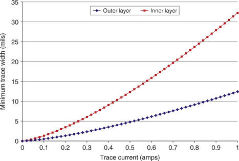 |
| Figure 6-38 Minimum trace widths for 1
oz copper for Δ
T = 10°C. |
Note: The glass transition temperature for FR4 is −125 to 135°C, so as ambient temperature increases, the allowed Δ
T decreases and minimum trace width increases. Even if the board will be at room temperature, giving you a Δ
T = 108°C, it does not hurt to restrict the temperature rise intentionally just to be safe (e.g., specify Δ
T = 20°C even if it could be much higher).
Note: Equation (6.17) was derived from the IPC-2221A standard. Please refer to the standard for the actual equation and additional details.
You can usually use any of the standard technology files for most small signal applications. Figure 6-38 shows the minimum trace widths for l-oz inner and outer layer copper with Δ
T = 10°C. With 6-mil traces you can run up to about 300
mA on inner traces and about 600
mA on the outer traces, but for manufacturability and reliability considerations, they should be as wide as practical. Usually the applications of concern are power supply lines for large circuits and power supply boards in general.
Trace Width for Controlled Impedance
Controlled impedance PCB can be significantly more expensive than standard process PCBs. Before going through the effort and expense of designing controlled impedance transmission lines on the PCB, it is a good idea to determine if they are needed by determining if traces are electrically long (and whether controlled impedance is required).
For digital systems, at a minimum, we want the propagation time, PT, to be less than the rise time of the driver (i.e., PT < ½RT or RT > 2PT). From the discussion under Reflections another way to look at it is that the length of the trace,
Ltrace, should be less than one half of the special extent (edge distance) of the rising edge (i.e.,
Ltrace < ½
LSE or
LSE>2
Ltrace). To determine if this condition is met we need to determine RT and PT. RT (or fall time—FT) can be obtained from the data sheet for the device that is driving the trace and will have units of time (e.g., nanoseconds). Note that, since both the rise and the fall times must fall within limits, the smaller value should be used in the calculations. The RT and FT of several logic families are listed in Appendix C.
To calculate PT we need to know the intrinsic propagation delay (
tPD), which has units of time/distance. The intrinsic propagation delay for various transmission line configurations is given in Table 6-6 and Table 6-7. Bracketed numbers [1][2][3][4][5][6][7][8][9][10][11] and [12] refer to the numbered references at the end of the chapter.
Topologies,
Z0,
tPD, Trace Width, and Trace Separation Design Equations for Various Transmission Lines
Units for
h, w, and
t can be mils, centimeters, inches, etc., as long as they are consistent.
Note that in general the values of intrinsic capacitance (
C0) and intrinsic inductance (
L0) are given by [1] and
and
 where
C0 is in picofarads per inch,
tPD is in picoseconds per inch, Z
0 is in ohms, and
L
0 is in nanohenrys per inch.
where
C0 is in picofarads per inch,
tPD is in picoseconds per inch, Z
0 is in ohms, and
L
0 is in nanohenrys per inch.
For values of
C0 and
L0 that are specific to particular transmission line topologies, please see the appropriate references as listed.
There are two families of transmission lines described here, microstrip and stripline, including their subfamilies, which are as follows:
Microstrip:
1. Surface microstrip,
2. Surface differential microstrip,
3. Embedded microstrip, and
4. Embedded differential microstrip.
Stripline:
1. Balanced (symmetric) stripline,
2. Unbalanced (asymmetric) stripline,
3. Broadside coupled differential stripline (symmetric), and
4. Edge coupled differential stripline (symmetric and asymmetric).
Next calculate the propagation time, PT, using Eq. (6.18),
 where PT is a trace’s one-way propagation time,
Ltrace is the length of the trace as measured on the PCB, and
tPD is the intrinsic propagation delay from Table 6-6 and Table 6-7.
where PT is a trace’s one-way propagation time,
Ltrace is the length of the trace as measured on the PCB, and
tPD is the intrinsic propagation delay from Table 6-6 and Table 6-7.
(6.18)
If it is determined that the trace is electrically too long, then either it needs to be shortened or the impedances need to be matched. To determine the maximum allowable trace length use Eq. (6.19).
Since we want PT<1⁄2RT and PT =
Ltrace×
tPD, then

(6.19)
For analog systems we determine the critical length of a trace with respect to the wavelength rather than the rising edge. The wavelength, λ, is determined using Eq. (6.20),
 where
v
P is the intrinsic propagation velocity (
v
P = 1/
tPD) and
f is the frequency of the signal on the trace.
where
v
P is the intrinsic propagation velocity (
v
P = 1/
tPD) and
f is the frequency of the signal on the trace.
(6.20)
Various trace length limits are stated in the literature: anywhere from
Ltrace < 1/6λ to
Ltrace < 1/20λ. IPC-2251 recommends
Ltrace < 1/15λ, where
Ltrace is the length of the trace as measured on the PCB and λ is the wavelength of the highest frequency component of the signal (the shortest wavelength).
Table 6-6 and Table 6-7 can be used to determine
tPD (ps/in.) for critical length calculations for both analog and digital circuits. If it is determined (using Eq. [6.19] or [6.20]) that a trace is electrically long, then source and load resistance and the transmission line impedance need to be controlled.
To design a controlled impedance transmission line on a PCB use Table 6-6 and Table 6-7 to determine the trace width,
w (in.). The trace thickness,
t (oz/ft
2), dielectric thickness,
h (mils), and dielectric constant, ε
r (unitless), are determined by your board manufacturer.
There is another type of transmission that is not in Table 6-6 and Table 6-7: The coplanar transmission line is shown in Figure 6-39. Typically
d <
h, and
w is relatively wide compared to the other configurations. The copper along each side of the trace is a topside return plane and is typically >5
w in both directions. The bottomside return plane is not present in some applications.
 |
| Figure 6-39 A coplanar transmission line. |
The equations are not well documented in the literature for this type of coplanar configuration except in the
Transmission Line Design Handbook, by Brian C. Wadell (1991). The equations are not presented here because they are rather unwieldy, and this type of transmission line is not widely used on FR4. If you need to use this type, please see the reference for a full description of its design, use, and limitations. An approximation of this type of configuration is sometimes attempted using guard traces and copper pours, but because of the relative dimensions (i.e.,
h <
d or
h ≈
d), an accidentally designed surface microstrip is usually the result.
Trace Spacing for Voltage Withstanding
There are two reasons for controlling the spacing between traces: (1) to ensure adequate voltage-withstanding capability (insulation resistance) between high voltage lines and (2) to minimize cross talk between signal lines. Table 6-8, which is an abridged version of a similar table given in IPC-2221A (Table 6-1),shows the required trace spacing for various voltage ranges on internal and external layers. The spacing on external traces depends on both the voltage and the external coating of the board.
Trace Spacing to Minimize Cross Talk (3w Rule)
The default trace spacing used in PCB Editor’s Constraint Manager is shown in Figure 6-40(a), in which the edge-to-edge spacing between traces is typically one conductor width. If a trace is susceptible to cross talk from adjacent traces then it should be kept a minimum of two trace widths (edge to edge) from the other traces, as shown in Figure 6-40(b). This is referred to in the references as the 3
w rule because the center-to-center spacing is 3
w, as indicated in Figure 6-40(b). At 3
w, the traces are out of reach of about 70% of each other’s magneticfield if the traces are controlled impedance transmission lines (or reasonable approximations). Keeping the traces 10
w apart at the centers will keep the traces out of about 98% of each other’s field (Montrose 1999, p. 210).
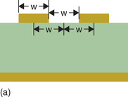 |
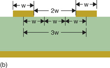 |
| Figure 6-40 Trace spacing methods: (a) typical trace spacing, (b) 3w spacing to minimize cross talk. |
To adjust the trace-to-trace spacing in PCB Editor select the
Constraint Manager button on the tool bar to display the Constraint Manager as shown in Figure 6-41. Select the
Spacing tab and the
Line icon as shown. Enter the edge-to-edge spacing in the
Default row or click the ‘ + ’ box and enter edge-to-edge values for specific nets.
 |
| Figure 6-41 Setting the trace spacing in PCB Editor’s Constraint Manager. |
Traces with Acute and 90° Angles
Routing high-frequency analog or high-speed digital traces with acute or 90° angles has long been discouraged, but not everyone agrees anymore as to how much of a problem it really is (see Jonson and Graham 1993, p. 174; Montrose 2000, p. 220; Bogatin 2004, p. 317; and Brooks 2003, p. 383). The argument is that the trace width increases by a factor of 1.414 at the corner of the trace (as shown in Figure 6-42) and causes a change in the characteristic impedance (due to an increase in capacitance) of the trace. As discussed above impedance mismatches cause reflections. The reflections in turn cause ringing in digital circuits with fast rise times and standing or traveling waves in high-frequency analog circuits. In theory then, 90° corners should be avoided—at least when routing controlled impedance transmission lines.
 |
| Figure 6-42 Trace geometry of a sharp 90° corner. |
A look through the references shows that, when using high-end network analyzers and time domain reflectometers to measure the reflection from a 90° corner, the effects are evident (Bogatin 2004, p. 318). However, the frequencies at which the reflections occur are high (into the upper gigahertz for traces greater than 50 mils wide and tetrahertz for traces less than 10 mils), and compared to other sources of impedance discontinuities (such as vias), the effects are insignificant.
Another thing to consider is that (with PCB Editor anyway) the corners are not as sharp as shown in Figure 6-42. Recall from Chapter 1 that pads and traces are drawn as flashes or draws, respectively, by photoplotters with apertures of a given diameter. While square apertures can be used (and are for square pads), PCB Editor uses round apertures for traces in the Gerber codes. A 90
° corner produced by PCB Editor is shown in Figure 6-43(a). Although the corner may look fairly sharp, a close-up of the corner shown in Figure 6-43(b) shows that the outer edge is rounded and only the inner corner is square. This results in a smaller increase in width than with a square corner.
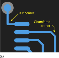 |
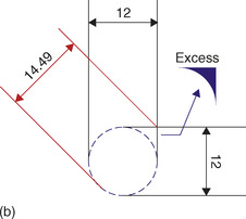 |
| Figure 6-43 Geometry of a 90° corner in Layout: (a) 90° and chamfered corners, (b) excess copper at a 90° corner. |
The difference between a 12-mil trace and a 17-mil trace (at the sharp corner in Figure 6-42) is about 11.5
Ω for a dielectric constant of 4.2 and a core thickness of 10 mils, and the difference between the 12-mil trace and a 14.5-mil trace (at the rounded corner in Figure 6-43) is about 6.2
Ω. However, the effect of extra width (and change in impedance) is very small. The excess area shown in Figure 6-43(b) is 7.73 mils
2 for a 12-mil trace. If the equivalent area is divided by 2 and each piece is placed on either side of a straight segment of a 12-mil trace (as indicated by the arrow in Figure 6-44) it is clear that the excess area created by the 90° corner is insignificant compared to other factors such as vias and land patterns. The literature (Brooks 2003, p. 385) suggests that even acute angles of 135° can be used up to about 1
GHz.
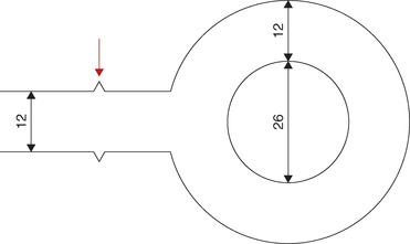 |
| Figure 6-44 Excess area compared to a typical via (Brooks 2003, p. 383; Johnson and Graham 1993, p. 174; Montrose 1999, p. 220; Bogatin 2004, p. 315). |
Using PSpice to Simulate Transmission Lines
PSpice is used in Chapter 7 to develop PSpice subcircuit models for creating new Capture parts with simulation capabilities. In this section PSpice is used to simulate transmission lines. When used in conjunction with the design equations from this chapter and the simulations in the PCB Design, Examples, PSpice can be of help in designing PCB-based transmission lines and in understanding transmission lines in general.
The circuit shown in Figure 6-45 is used here to simulate a high-speed digital circuit (it was also used previously to generate the plots used to explain ringing). The circuit consists of a driver gate with an output impedance of 10
Ω, a 50-Ω transmission line, and a receiving gate with in input resistance of 1
kΩ and input capacitance of 15
pF. The PSpice parts used in the circuit are
V2 is
VPULSE (from the Source library), the driver.
R1 is
R (from the Analog library), the source resistance (output impedance) of the driver.
T1 is
T (from the Analog library), the transmission line.
R2 is
R (from the Analog library), the load resistance.
C1 is
C (from the Analog library), the load capacitance.
 |
| Figure 6-45 A basic transmission line simulation circuit. |
Figure 6-45 also shows the various reflection coefficients at the impedance mismatches, where the reflection coefficient looking into T1 from R1 is
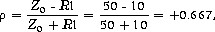 the reflection coefficient looking into R1 from T1 is
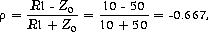 and the reflection coefficient looking into R2 from T1 is
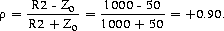
To simulate a transmission line (T1) the characteristic impedance,
Z0, must be specified and either the transmission delay (TD) must be specified or the frequency (
f) and number of wavelengths (NL) must be specified. Use TD for digital signals, and use
f and NL for analog signals.
Simulating Digital Transmission Lines
The value TD is the same as PT (propagation time) from the earlier discussion and is calculated by
 where
tPD is found from Table 6-6 and Table 6-7. For the surface microstrip
tPD is
where
tPD is found from Table 6-6 and Table 6-7. For the surface microstrip
tPD is
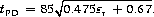
In laying out a digital circuit (for instance the digital design example in the PCD Design Examples), it is important to know the critical trace length so that traces can be kept short enough and parts can be placed accordingly. The critical trace length is calculated by
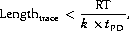 where
k is a safety factor and is essentially the ratio PT/RT. The maximum trace length recommended is
k = 2; larger values of
k (shorter traces) are better.
where
k is a safety factor and is essentially the ratio PT/RT. The maximum trace length recommended is
k = 2; larger values of
k (shorter traces) are better.
For ALS family logic RT is approximately 2
ns. Using ε
r = 4.2 the critical trace length is then 7.3 in. Table 6-9 shows the effective
k value and TD for various transmission line lengths.
| Long | Critical | Safe | |
|---|---|---|---|
| Length trace (in.) | 30 | 7.3 | 3.5 |
| k (approximate) | ½ | 2 | 4 |
| TD (ns) | 4.1 | 1 | 0.24 |
Knowing RT (2
ns) and TD (from Table 6-9), we can use PSpice to simulate the various transmission line lengths. Set up the PSpice simulation as shown in Figure 6-46. To display the
Simulation Settings dialog box select
Edit Simulation Profile from the
PSpice menu. Note: If the step time is too large, the simulation may become unstable and you will not get good results. A maximum step size of 1/1000 of the total run time usually produces satisfactory results. Click
OK.
 |
| Figure 6-46 PSpice simulation settings. |
To start the simulation, press the blue triangle on the menu bar, or press
F11 on the keyboard, or select
Run from the
PSpice menu. The results are shown in Figure 6-47Figure 6-48 and Figure 6-49.
 |
| Figure 6-47 Simulation results for a long line (
k = ½). |
 |
| Figure 6-48 Simulation results for a critical length line (
k = 2). |
 |
| Figure 6-49 Simulation results for a short line (
k = 4). |
Simulating Analog Signals
For analog signals
f is the frequency on the trace and NL is the length of the trace in relative wavelengths (e.g., NL would be 0.25 for a quarter wavelength trace at frequency
f). To determine NL you need to know the wavelength, λ. You can calculate the wavelength using Eq. (6.21):
 where
where
(6.21)
vPD is the propagation velocity (distance/time) of a wave through a dielectric.
f is the frequency of the wave.
tPD is the propagation time (time/distance) as described above.
So for a 66-MHz signal traveling through the same surface microstrip from the above example (ε
r = 4.2), λ = 110.8 in. The critical length for traces carrying analog signals varies depending on which book you read but is often cited as being λ/6, λ/15, or λ/20 (or somewhere in between). As with the digital signals, the shorter the trace, the better.
References
E. Bogatin,
Signal Integrity—Simplified.
(
2004)
Pearson Educational,
Upper Saddle River, NJ.
D. Brooks,
Signal Integrity Issues and Printed Circuit Board Design.
(
2003)
Pearson Educational,
Upper Saddle River, NJ.
IPC-2141. 1996.
Controlled Impedance Circuit Boards and High Speed Logic Design. Northbrook, IL: IPC-Associated Connecting Electronics Industries.
IPC-2221A. May 2003.
Generic Standard on Printed Board Design. Northbrook, IL: IPC-Associated Connecting Electronics Industries.
IPC-D-330
.
H. Johnson, N. Graham,
High-Speed Digital Design: A Handbook of Black Magic.
(
1993)
Prentice Hall,
Upper Saddle River, NJ.
M.I. Montrose,
EMC and the Printed Circuit Board: Design, Theory, and Layout Made Simple.
2nd edn. (
1999)
IEEE Press,
New York.
M.I. Montrose,
Printed Circuit Board Design Techniques for EMC Compliance: A Handbook for Designers.
2nd edn. (
2000)
IEEE Press,
New York.
R.A. Serway,
Physics for Scientists and Engineers with Modern Physics.
3rd edn. (
1992)
Harcourt Brace Jovanovich,
Orlando, FL.
B.C. Wadell,
Transmission Line Design Handbook.
(
1991)
Artech House,
Norwood, MA.
Numbered References
[1]
IPC-2251. November 2003.
Design Guide for the Packaging of High Speed Electronic Circuits, p. 32. Northbrook, IL: IPC-Associated Connecting Electronics Industries.
[2]
IPC-2141. 1996.
Controlled Impedance Circuit Boards and High Speed Logic Design, p. 12. Northbrook, IL: IPC-Associated Connecting Electronics Industries.
[3]
M.I. Montrose,
Printed Circuit Board Design Techniques for EMC Compliance: A Handbook for Designers.
p. 1012nd edn. (
2000)
IEEE Press,
New York.
[4]
M.I. Montrose,
EMC and the Printed Circuit Board: Design, Theory, and Layout Made Simple.
p. 1722nd edn. (
1999)
IEEE Press,
New York.
[5]
IPC-2251. November 2003.
Design Guide for the Packaging of High Speed Electronic Circuits, p. 36. Northbrook, IL: IPC-Associated Connecting Electronics Industries.
[6]
M.I. Montrose,
Printed Circuit Board Design Techniques for EMC Compliance: A Handbook for Designers.
p. 1072nd edn. (
2000)
IEEE Press,
New York.
[7]
M.I. Montrose,
EMC and the Printed Circuit Board: Design, Theory, and Layout Made Simple.
p. 1772nd edn. (
1999)
IEEE Press,
New York.
[8]
M.I. Montrose,
Printed Circuit Board Design Techniques for EMC Compliance: A Handbook for Designers.
p. 1032nd edn. (
2000)
IEEE Press,
New York.
[9]
M.I. Montrose,
EMC and the Printed Circuit Board: Design, Theory, and Layout Made Simple.
p. 1772nd edn. (
1999)
IEEE Press,
New York.
[10]
IPC-2251. November 2003.
Design Guide for the Packaging of High Speed Electronic Circuits, p. 33. Northbrook, IL: IPC-Associated Connecting Electronics Industries.
[11]
M.I. Montrose,
Printed Circuit Board Design Techniques for EMC Compliance: A Handbook for Designers.
p. 1052nd edn. (
2000)
IEEE Press,
New York.
[12]
IPC-2251. November 2003.
Design Guide for the Packaging of High Speed Electronic Circuits, p. 35. Northbrook, IL: IPC-Associated Connecting Electronics Industries.
..................Content has been hidden....................
You can't read the all page of ebook, please click here login for view all page.