Chapter 3. Project Structures and the PCB Editor Tool Set
This chapter explains what you did when making the simple design in Chapter 2 and why. It also introduces and describes the PCB Editor tool set in greater detail, so that you will be well equipped to lay out more complicated boards in the PCB Design Examples in Chapter 9.
Project Setup and Schematic Entry Details
Capture Projects Explained
When you set up your project by following the
File → New → Project menu path, you had five options from which to choose: a project, a design, a library, a VHDL file, or a Text file. The options we are most interested in are projects and libraries, and we look at those in great detail throughout the book. VHDL files are used in field programmable gate array projects and are not discussed here. A Text file is simply a text file (for making project notes, for example).
After you selected the
New Project option to begin setting up your project, four more options were available to you in the
New Project dialog box:
Analog or Mixed-Signal A/D,
PC Board Wizard,
Programmable Logic Wizard, or
Schematic. A flow diagram of these options and suboptions is shown in Figure 3-1 (see also Figure 2-2).
Analog or Mixed-Signal A/D is used to simulate analog and/or digital circuits using PSpice. PSpice is used to develop and test models (Chapter 7), perform circuit simulations (Chapter 7 and the PCB Design Examples), and simulate transmission lines (PCB Design Examples). For now, we work mostly with the second option, the
PC Board Wizard, while we focus on designing PCBs. The next option,
Programmable Logic Wizard, is for working with programmable devices and is not discussed in this text. A
Schematic is basically just a design file with only a schematic and a parts cache. The thick green line in Figure 3-1 shows the path you followed in Chapter 2, that is,
File → New → Project → PC Board Wizard → No Simulation.
 |
| Figure 3-1 New Project design flow and options. |
There are four types of OrCAD libraries. As shown in Figure 3-2, these four libraries have three file extensions. There are two types of OLB libraries: an LIB library and a symbols library, which contains .dra files as well as some other files that are explained in detail in Chapter 8. Inside the capture folder is a library folder, which contains one of the types of OLB files, and a folder called
pspice, which contains the other types of OLB files. The OLB files located directly in the Capture library folder contain simple schematic part symbols and are the ones we used in Chapter 2. The libraries located in the pspice folder contain parts with schematic symbols, too, but the parts also contain PSpice templates, which are links to specific PSpice models. The PSpice models to which templates point are located in the main OrCAD pspice folder (shown at the bottom of Figure 3-2). Individual models are grouped into various PSpice library files, which contain the .LIB extension. The share folder contains the footprint models (called
symbols), which are files with the .dra extension. Most parts in Capture are capable of having a PSpice template or a footprint assigned to them, but only some parts have them preassigned. It may seem backward, but only parts from the PSpice part library (located in the Capture/library folder) have preassigned templates and footprints, and the footprints are OrCAD Layout footprints not PCB Editor footprints. So, in Chapter 2, when you worked with the PCB Project Wizard, you selected libraries from the Capture/library folder, which had parts with schematic symbols but had no PSpice simulation capabilities or footprints assigned to them.
 |
| Figure 3-2 OrCAD libraries (extraneous files not shown). |
Once you clicked
Finish in the
PCB Project Wizard box, Capture opened up the
Project Manager window shown in Figure 3-3. Behind the scenes, Capture generated two files: an OrCAD project file (name.OPJ) and a design file (name.DSN). These files will be in the directory you chose when you set up the project.
 |
| Figure 3-3 Project Manager window. |
As you look at the
Project Manager window, you can see that a project contains three folders labeled
Design Resources,
Outputs, and
Referenced Projects. Initially, the
Outputs and
Referenced Projects folders are empty. When a netlist is created, netlist files are placed in the
Outputs folder. The
Design Resources folder contains one design (represented by the icon) and a
Library folder. A project can have only one design, but a design can have several subfolders, which in turn may contain several different items. The
Library folder contains links to the libraries used by your design. We discuss library management in Chapter 7. The design contains at least one Schematic folder (the root folder) and a
Design Cache folder. A design can contain multiple Schematic folders, and each Schematic folder can contain multiple schematic pages. The
Design Cache folder contains a record of each part you used in your design. If you modify one of the parts on a Schematic page, Capture makes a copy of it (leaving the original part in the library unchanged) and adds a record of the modified part to the design cache. A design with one Schematic folder and one or more Schematic pages connected together by off page connectors is called a
flat design. A design with more than one Schematic folder and one or more Schematic pages per folder or that contains hierarchical blocks is called a
hierarchical design. Hierarchical designs are not discussed here, since they are not used with PCB design projects. For more information on project details, see Chapter 2 of the
Capture User’s Guide, under “Starting a New Project” (cap_ug.pdf in the OrCAD_16.0/DOC folder).
Capture Part Libraries Explained
Once the project is set up, the next step is to open the Schematic page (if it is not already open) and begin placing parts from the
Place dropdown menu. When the
Place Part dialog box opens (see Figure 3-4), it shows a list of libraries (in the
Libraries window) and a list of the parts (in the
Part List window) within a library. If you select a part within one of the libraries, you can see what the part looks like in the preview window, as pointed out in Figure 3-4(a). The libraries listed in the
Libraries window are ones that were added by the PC Board Wizard when you set up the current project and libraries that were added to the list during previous projects. You can add other libraries to the list by clicking the
Add Library… button. Likewise, you can remove a library from the list by selecting it and clicking on the
Remove Library button. The libraries that are listed may be from the Capture or the PSpice library. It is not obvious which library it is from just by looking at the name, (compare Figures 3-4(a) and 3-4(b)). However, if you have Windows ToolTips turned on and hold your mouse over the library name, the ToolTips text box will show the path of the library, (see Figure 3-4(a)). From the path, you can tell which type of library it is. Another important note is that, if a PSpice or Layout library (not a PCB Editor library) is associated with the Capture part, you will see one or both of the icons below the part preview window, as shown in Figure 3-4(b). If no icons are present, it means that it is just a Capture schematic part that has no footprint or PSpice template (models) assigned to it.
 |
 |
| Figure 3-4 Place Part from Capture or Capture/PSpice library: (a) Capture parts, (b) PSpice parts. |
As you place parts in your design, Capture keeps track of the parts and stores the information in a database file generated the moment you place your first part. This file has a .DBK extension. After you finish your design and tell Capture to make the PCB Editor netlist, Capture generates three more files that describe which parts were used and how they were connected. The files are
pstxnet.dat (the netlist file),
pstxprt.dat (the reference designator and device type file), and
pstchip.dat (a device definition file also used for pin swapping, etc.); and they are located in the
Outputs folder. These files are also used when back-annotating information from PCB Editor to Capture. More on back-annotation is discussed in the PCB Design Examples. For the most part, these files are used behind the scenes, and you need not know much about them for what we cover in this text. If you want to know more about them, please see
Allegro® PCB Editor Users Guide: Transferring Logic Design Data (algrologic.pdf, p. 18) which is located in the OrCAD documents folder.
Another file that gets created is the netrev.lst file, which is a netlisting report generated when the PCB Editor netlist files are created. If there is a problem during the netlisting process, this is where the errors and warnings are documented. If you have trouble trying to create a netlist, open this file with Microsoft Word or another text application and search for the word
error or
warning. An example of a netlist error is given in the PCB Design Examples.
Understanding the PCB Editor Environment and Tool Set
Terminology
Before we start talking about the tool set, we examine a couple terms that should be defined up front, so the descriptions of the tools make more sense. These important terms follow:
▪
Classes and
subclasses—another way of thinking about layers and objects on layers. From the PCB perspective, there are layers: routing layers, plane layers, soldermask layers, and the like. But being able to group or separate things into classes gives you more control over the design. Generally speaking, a class is a broad grouping of things and a subclass is a more specific thing that can be grouped into a class. For example, Etch (defined later) is a class, and Top and Bottom Etch are subclasses of Etch. Some subclasses are distinct but have the same name. They are distinct because they belong to different classes. An example of this situation is the Silkscreen subclass, one of which belongs to the Board Geometry class (lines or text belonging to the board), another belongs to the Component Reference (text only, belonging to components only) class, and yet another belongs to the Manufacturing class (a grouping of all types of the other two subclasses). By having separate subclasses of silkscreen (or soldermask, say), you can control the color and visibility of each type of silkscreen object. As you go through the design examples, this will become very clear.
▪
Clines—where
cline is short for connection line. A cline is a routed copper trace that makes electrical connections to pins. Clines are also called
etch. Unrouted connection lines are called
nets or
rat’s nest. Lines that make up graphic objects are just lines.
▪
Etch—objects on routing and plane layers that become copper patterns during the manufacturing process. Etch objects are on subclasses that belong to the Etch class and can be traces (clines), areas (rectangles), or text. Etch objects can be connected to nets or may stand alone.
▪
Elements—a general term for things that you put into your board design. You can have text elements, graphic elements (e.g., silkscreen outlines), and components (footprint symbols).
▪ Frectangle—a filled rectangle. A frectangle is drawn using one of the Shape tools as described later. Frectangles can have special properties, and not all rectangles are frectangles. Some of the differences between plain rectangles and frectangles are described later. There are also dynamic copper shapes, which can be rectangles but are different from frectangles. Frectangles and dynamic copper objects are demonstrated in the design examples.
▪
Symbols—elements you can place in your design that can be made up of one or more other elements. For example, a component footprint is called a
symbol (specifically a footprint symbol), which can comprise padstacks, outline details, and text elements. Other types of symbols include flash symbols, mechanical symbols, and drawing symbols, to name a few. Symbols are used extensively in Chapter 8 and the PCB Design Examples.
▪
Functions—a part of an integrated circuit (e.g., a logic gate).
PCB Editor Windows and Tools
At this point in Chapter 2, PCB Editor was launched, the board design (
name.brd) was opened with all default settings, and a blank work area was presented to you. From this point you made a board outline, placed the parts on your board, autorouted the board, and produced the artwork for it. To be fluent at these tasks, you need to know how to use the PCB Editor tools. We now take a tour of the PCB Editor environment and tool set.
Note: From the time you start your design in Capture to the time the artwork is produced in PCB Editor, nearly 30 files can be generated, which together fully describe your design. If you save more than one project in the same folder, it can become very cluttered. It is a good idea to set up a “MyProjects” folder that contains subfolders for each project.
The Design Window
The
Design window is the working environment for a board design (see Figure 2-12). From the
Design window, you have access to the tools you need to handle parts, route traces, and perform back annotations (design updates from PCB Editor to Capture). Hundreds of tasks can be executed from the
Design window menus. Since they are covered in detail in the
Allegro®
User’s Guide, a detailed discussion of the menus is not given here, but the key menu options are discussed in the Examples as the need arises. The toolbar is discussed next.
The Toolbar Groups
By default, two toolbars are displayed. You can move them wherever you want or turn them off.
To add tool bars, select
View → Customize Toolbar… from the menu. This section does not describe the tools in great detail but serves as an introduction only. The use of the tools are demonstrated in the design examples and described further in
Allegro®
PCB Editor User Guide: Getting Started with Physical Design (algrostart.pdf).
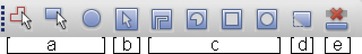
APPLICATION MODE GROUP

PCB Editor works in two application modes: [a]
Generaledit and [b]
Etchedit. The differences between the two modes are subtle, and most of the time you need not consciously choose between one or the other. The biggest difference between the two modes is which items are available and checked by default in the
Find pane and which ones of those items are higher up in selection priority. When in General Edit mode, the highest level hierarchical type elements (items at the top of the list) enabled by the
Find filter are highlighted by default and become more easily selectable with your mouse. But in Etch Edit mode, the lowest level hierarchical type elements enabled by the
Find filter (items at the bottom of the list) become more easily selectable. You can execute most commands in either mode, but you will find that some commands are easier to perform in one mode than the other and you may have to wrestle with the
Find and
Options panes settings to do so. You can determine which application mode you are in by looking at the application box in the status bar (described later). See
Allegro®
PCB Editor User Guide: Getting Started with Physical Design (algrostart.pdf) for further information.
EDIT GROUP
The edit group is made up of the following tools: [a] Move, [b] Copy, [c] Delete, [d] Undo/Redo, and [e] Fix/Unfix. These tools can be used on graphical objects, text, and etch. The Delete tool deletes (erases) objects, but it is used to rip up traces (it does not delete nets) and unplace parts. The Fix/Unfix tool is used to prevent objects (e.g., shapes and text) from being moved or deleted, and it prevents routed traces (clines) from being ripped up.
VIEW GROUP
a. Unrats All/Rats All—controls the visibility of all unrouted nets (also know as
rat’s nest). You can also control the visibility of individual nets using the
Rats Off property with the Constraint Manager (described later) or by selecting
Unrats All then selecting
Display → Show Rats → Net in concert with the
Find filter tab to then display specific nets.
c. Redraw—refreshes the display.
SETUP GROUP
The following tools constitute the setup group:
a. Grid Toggle—allows you to turn the grids on or off. The displayed grid resolution depends on the settings in the
Define Grid dialog box (from
Setup menu) and the type of layer (class) that is active. Classes related to etch layers use the
Etch grid resolution and non-etch-related classes use the
Non Etch resolution. If the grid resolution is too dense for a given Zoom level, PCB Editor automatically adjusts the grid density view but not the functionality.
b. Color Pallet—allows you to control the color and visibility of classes and subclasses. The
Color dialog box is described in greater detail later.
c. Shadow Toggle—controls the intensity of visible layers. Shadow mode makes highlighted items stand out more clearly.
d. Stack-up—launches the
Layer Cross Section dialog box, where you define your board’s stack-up as described later.
e. Constraint Manager—launches the Constraint Manager, where you set autorouter specifications (e.g., trace width and spacing) and design rule constraints. The Constraint Manager is discussed further later.
f. Keep-in Router.
g. Keep-in Package—automatically selects the correct classes and drawing tools so that you can quickly draw these areas in your board design.
SHAPES GROUP
These are drawing tools and are different from the
Add (line and rectangle) group objects described later. They are used to make shapes that interact with the DRC tool and are used to create dynamic shapes that adjust automatically (e.g., plane layers that heal and you can plow through) when interacting with other Etch objects. You can also make static shapes with them, which are used for keep-in/-out areas and the like. Shapes can be filled or unfilled, static or dynamic. Some classes, such as the Package Keep-in class, automatically know what type of shape it needs (unfilled), so even if you unknowingly choose a static filled rectangle, it will automatically become unfilled. Many other classes do not. For example, you can place a filled rectangle on the GND plane, but it may not connect to pins properly. Copper areas on negative plane layers should be Dynamic shapes.
a. Shape Tools—The following tools are used to make the shapes: Shape Add (polygon), Shape Add Rect(tangle), and Shape Add Circle.
b. Shape Select—used to edit existing shapes (stretch shapes, add or move vertices, etc.).
c. Shape Void tools—are used to remove areas of shapes. For example, if you want to create an opening in the plane layers because a mounting hole is inserted in the design and has a route keep-out area, then you can use a void shape to make the opening.
d. Edit Shape Boundary—is used to add or remove areas to a shape at the shape’s boundaries. It is similar to using the Merge and Void commands but is easier to use and can be used only on the edge of a shape.
e. Island Delete—deletes pieces of planes or shapes that become detached from the main shape due to spacing requirements around groups of pins. These floating pieces can become EMI issues and should be removed.
Note: When making changes that affect dynamic shapes some changes may not take effect immediately. To redraw shapes, select
Display → Status → Update shapes from the menu.
MANUFACTURE GROUP
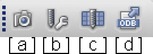
a. Artwork—opens the
Artwork Control Form dialog box, where you set up the classes and subclasses for which you want manufacturing data generated.
b. NC Drill Param(eters)—opens the
NC Parameters dialog box, where you can set up drill format (Enhanced Excellon format, etc.).
c. NC Drill Legend—is used to set up then display the drill legend (drill chart). Drill symbols in parts on your design then also become visible.
d. ODB—exports database information into a Valor ODB++ database, which contains all CAD/EDA, assembly, and manufacturing data. ODB is not enabled in basic OrCAD PCB Editor.
DISPLAY GROUP
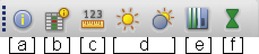
a. Show Element—displays a text box that provides information and properties about the object you select (nets, shapes, components, etc.). Use it in concert with the
Find filter to locate objects or nets without actually having to click on them.
b. Show Constraints—is similar to Show Element but reports only constraints.
c. Show Measure—measures the distance between two pick points and displays the measurement in a pop-up text box.
e. Highlight Sov—checks for cline segments (traces) routed over voids (not enabled in basic OrCAD PCB Editor).
f. Waive DRC—used to override DRCs that you know about and do not need or want to fix.
MISCELLANEOUS GROUP

a. Report—opens the
Reports dialog box so that you can pick a report to view (e.g., DRC, bill of materials). Selecting this button is the same as selecting
Tools → Reports from the menu.
b. DRC update—updates the DRC status. It does the same thing as selecting
Display → Status → Update DRC from the menu. You can then use
Display → Status to see how many errors there are, or you can use the
Report button to show the list of errors if there are any.
PLACE GROUP

a. Place Manual—displays the
Placement dialog box so that you can place parts or other objects from the list.
b. Place Manual–H—does the same thing as Place Manual but does not automatically show the
Placement dialog box. To show the dialog box, right click and select
Show from the pop-up menu.
ROUTE GROUP
a. Net Schedule—sets priorities on net routing. It is not enabled in basic OrCAD PCB Editor.
b. Add Connect—is used to manually route traces (produce clines).
c. Slide—is used to move or stretch a routed trace. It automatically uses autorouter algorithms to prevent most (but not all) DRCs.
d. Delay Tune—is used to route differential pairs. It is not enabled in basic OrCAD PCB Editor.
f. Vertex—is used to add a vertex to a line or cline (use shape select to add or move vertices on shapes).
g. Create Fanout—is used with
Setup → Design Parameters → Route → Create Fanout Parameters to define how fan-outs should be done. Select this tool then click on a pin or component to make it happen.
h. Spread between Voids—is not enabled in basic OrCAD PCB Editor.
ADD GROUP
These objects are graphical in nature only. Use these tools for making graphics and text on silkscreen and assembly layers. The tools are
a. Add Line.
b. Add Rectangle.
c. Add Text.
d. Edit Text.
Note: Edit text is used to change the text characters. If you need to change the text properties (size and spacing etc.), you need to use the
Options pane and
Setup → Design Parameters → Text → Setup Text Sizes.
Control Panel with Foldable Window Panes
The control panel is an area containing three tabs that show or hide collapsible window panes. The panes are shown in Figure 3-5 in their default condition (no tools or commands active). The panes are dynamic, so what is displayed depends on what tool is active or what type of object you selected at that moment. From these panes, you can control visibility and selectability of objects and what particular tools can do (extent of effect, etc.) when you use them. The panes are collapsible, so that they do not take up design window space, but you can pin them in place by toggling the stick pin icon. You can also close them altogether by clicking the
X in the upper right corner. To display them select
View → Window → Options/Find/Visibility from the menu bar. Each pane is described briefly. You see examples of them in action during the design examples.
 |
| Figure 3-5 Control panel window panes. |
VISIBILITY PANE
The
Visibility pane is a shortened version of the
Color dialog box (described later). It provides a handy way to turn on and off routing and plane layers (or specific elements on those layers). The colored boxes and check boxes are switches you can use to toggle on and off specific items or entire rows or columns. The colored box in the
Options pane (described later) works the same way, and with it, you can control the visibility of more elements using the class and subclass lists.
FIND FILTER PANE
The
Find pane acts as a selection filter for tools and commands. By selectively checking object boxes, you can restrict which objects will be selected when you perform mouse picks in your design. The order of the object types indicates a level of hierarchy, so if all objects are enabled and you attempt to perform a mouse pick in a congested area of your board, the top-down order indicates which object type will likely be picked. Unchecking an object prevents that type of object from being selected. Note: If you attempt to perform a command on an object and PCB Editor does not let you do it, check the
Find pane; chances are, the box for that type of object has been unchecked.
You can further narrow searches and selections by using the
Find By Name area. Select the type of thing you are looking for from the dropdown list then click the
More… button. A dialog box will pop up, which will allow you to pick specific objects from a list by name or property.
OPTIONS PANE
The
Options pane is very dynamic and you will use it often. Its appearance is determined by what tool you have selected or what command you are running. Figure 3-6 gives an example, where (left) shows what the
Options pane looks like when the Delete tool is active and (right) shows what the
Options pane looks like when the Add Connect tool is active. Along with the
Visibility pane and the
Color dialog box, you can turn on or off layers (classes) or parts of layers (subclasses) by toggling the colored squares. When you first start out learning PCB Editor, it is easy to forget about the
Options pane, but you want to keep it in mind, as it gives you significant control over your tools. You might want to pin this one up until you get used to relying on it.
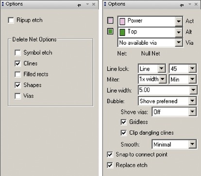 |
| Figure 3-6 Options pane with (left) Delete tool and (right) Add Connect tool active. |
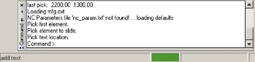
Command Window Pane
The
Command window (Figure 3-7) provides you with information, gives instructions, and allows you to enter commands at the Command prompt. Most of the commands you often use are also located on the toolbar and in the menus, but the
Command window can give you greater control of the tools (if you know the commands). The documentation folder in the OrCAD directory has manuals (called
command references) for these commands. The manuals are listed alphabetically by the first letter of the command followed by
coms. So, for example, if you are looking for instructions on how to use the
Command window to perform a manual routing task (
add connect) look in the
acoms document folder (or use the Online Help tool and search for Add Connect).
 |
| Figure 3-7 Command window pane. |
WorldView Window Pane
The
WorldView shown in Figure 3-8 is located in the lower right-hand corner of the design window and gives you a bird’s-eye overview of large boards. The white square represents your monitor, and the green outline represents the PCB’s outline.
WorldView is interactive. If you use the highlight tool and select a part or net (whether by clicking on it or by selecting it from a list using the
Find pane), the object will be displayed in the
WorldView. If you right click inside of it, a pop-up menu is displayed that lets you change the size and location of the view in the design area.
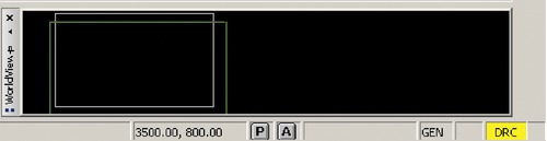 |
| Figure 3-8 WorldView window pane. |
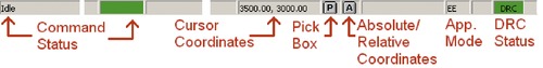
Status Bar
The status bar (shown in Figure 3-9) is located along the bottom of the design window, below the
Command window and
WorldView window. At the far left of the bar, the Command Status section lets you know if a command is active and running. If a tool has been selected (e.g., Move), the name or function of the tool is listed at the far left; and when a command is running, the colored box turns red. When the command has finished executing, the box turns green again.
 |
| Figure 3-9 Status bar. |
The
x,
y coordinates indicate the location of your cursor. The accuracy of the display is based on the design accuracy, which you can change in the
Design Parameters dialog box (select
Setup → Design Parameters → Design from the menu). The coordinates are absolute (based on the origin of the design) or relative (based on the last mouse pick). You can toggle between the two at any time using the
A (or
R) button, as described later.
The
P button is interactive. Clicking it produces a
Pick dialog box, which you can use to enter coordinate points in the work area using the keyboard rather than selecting a point with the mouse. This is useful for drawing outlines and so forth on large designs, so that you need not pan around the design trying to find and select a particular point. The
x and
y coordinates in the
Pick box are entered with space between them, not a comma.
The
A (or
R) button determines whether the coordinates are absolute or relative. Absolute coordinates show the cursor position relative to the design origin. Relative coordinates show the cursor
x and
y distance relative to the last pick point you made (whether a tool was active or not).
The
Application Mode text box informs you of whether PCB Editor is in Etch Edit (
EE) mode or General Edit (
GE) mode (described previously). The
DRC Status box lets you know at a glance if the design rule check is up to date and if any errors exist by the color of the box. If the box is any color other than green (see Figure 3-8), then you need to update the DRC and use a DRC report to locate any errors if they exist.
Color and Visibility Dialog Box
The
Color dialog box (Figure 3-10) is used to define custom colors for classes and subclasses and allows you to control the visibility of specific objects belonging to those classes (
Xs indicate the object is visible, open boxes indicate they are invisible). The
Color dialog box can be displayed by selecting the
Color button,
 , on the toolbar. As mentioned previously, the
Color dialog box performs some of the same functions as the colored and check boxes in the
Visibility and
Options panes, but as the figure shows, you have much greater control of objects and layers.
, on the toolbar. As mentioned previously, the
Color dialog box performs some of the same functions as the colored and check boxes in the
Visibility and
Options panes, but as the figure shows, you have much greater control of objects and layers.
| Color button
|
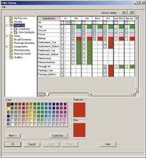 |
| Figure 3-10 Color dialog box. |
Layout Cross Section (Layer Stack-Up) Dialog Box
The
Layout Cross Section dialog box, shown in Figure 3-11, is where you define your board’s layer stack-up. From this dialog box, you can add or delete layers, define their physical and electrical properties (if you want to), and define positive and negative properties to routing and plane layers, respectively. The
Layout Cross Section dialog box is displayed using the
Xsection button,
 . Examples of setting up layer stack-ups are given in the PCB Design Examples.
| Xsection button
|
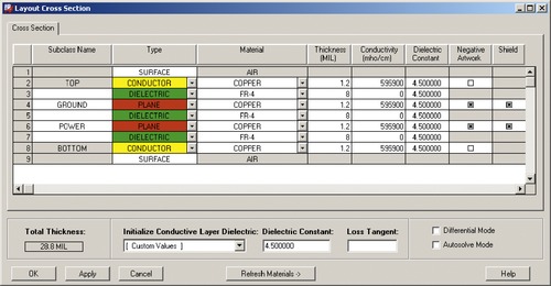 |
| Figure 3-11 Layout Cross Section dialog box. |
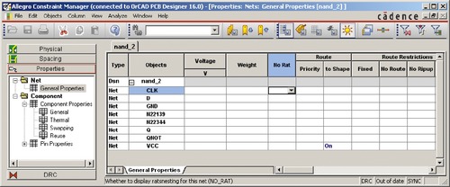
Constraint Manager
The Constraint Manager, shown in Figure 3-12, is where you set routing and component placement rules for your board design. The
Constraint Manager can be launched using the
Cmgr button,
 , by selecting
Setup → Constraints
… from the menu, or by typing
cmgr at the
>prompt in the
Command window. The
Constraint Manager has four tabs and each tab has several views (indicated by folders and icons). From these tabs and views, you have very precise control over routing characteristics for every net (e.g., trace width and spacing, what vias are used, routing enabled, locking traces, etc.), every component, and shapes.
, by selecting
Setup → Constraints
… from the menu, or by typing
cmgr at the
>prompt in the
Command window. The
Constraint Manager has four tabs and each tab has several views (indicated by folders and icons). From these tabs and views, you have very precise control over routing characteristics for every net (e.g., trace width and spacing, what vias are used, routing enabled, locking traces, etc.), every component, and shapes.
| Cmgr button
|
 |
| Figure 3-12 Constraint
Manager dialog box. |
Note: The
Constraint Manager takes a moment to load, but if it is taking a long time to load, check the
Command window. This tool will not load if a command is still active, and the
Command window (and
status bar) will tell you if that is the case. If so, you need to stop the current command by right clicking in the work space and selecting
Done from the pop-up menu.
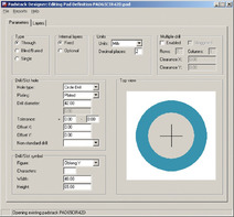
PADSTACK DESIGNER
The
Padstack Designer is used to define and modify padstacks (see Figure 3-13). The padstacks can be ones from the PCB Editor library or ones in a PCB design only. You use
Padstack Designer both during PCB layout work and separately during footprint development.
Padstack Designer can be launched from within PCB Editor (from the
Tools menu) or in stand-alone mode from the Windows
Start menu. Many examples of using the
Padstack Designer are presented in Chapter 8 (footprint design examples) and the PCB Design Examples.
 |
| Figure 3-13 Padstack Designer. |
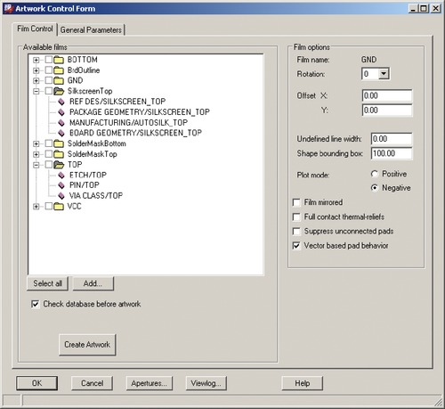
Manufacturing Artwork and Drill Files
Once the board is laid out and routed, the artwork must be generated. The information in the board design is separated into specific data files (Gerber files), which are used by the board manufacturer to make the different parts of your board. The
Artwork Control Form (Figure 3-14) is used to specify all the different types of layers for which Gerber files will be created and the format of the files. You can add as many layers as necessary to fully define your board design. Chapter 10 describes how to set up the
Artwork Control Form based on a board layout example.
 |
| Figure 3-14 Artwork Control Form dialog box (
Film Control tab). |
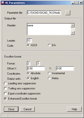
The drill files are generated by selecting
Manufacture → NC → NC Drill… from the menu. The drill files are generated from drill settings that you specify in the
NC Parameters dialog box (shown in Figure 3-15). The use of this dialog box is discussed further in Chapter 9.
 |
| Figure 3-15 NC (drill)
Parameters dialog box. |
The number and types of files generated by the
Artwork Control Form depends on the complexity of your board and the requirements of your board manufacturer. Most of the artwork files correspond to the layers with which you work in the layout environment, but some of the files do not. For example, files are generated for etch and silkscreen layers and drill files, all of which depend on the output format you chose. The two most common types of output formats are RS-274D and RS-274X (also known as
Excellon). The Excellon format is typically used, but your board manufacturer should tell you which specific files it needs and which format it prefers. Artwork instructions are set up from the
Manufacture → Artwork menu, and we will look at specific settings in Chapter 9.
Understanding the Documentation Files
Some of the terminology used in the PCB fabrication business is left over from the early PCB manufacturing days.
Drill tapes and
apertures are such terms. Nowadays, a drill tape is just an electronic file that describes drill holes and sizes just like any of the other files describes its data. However, originally the drill tape was actually a role of paper or Mylar with holes punched into it that described hole sizes and locations for early computer numerical control (CNC) machines, but it is still sometimes called a
drill tape. Here is another example. In Chapter 1, the current technology of photoplotting and laser direct imaging was discussed. In contrast, the older technology used a xenon flash lamp and a shutter to expose photosensitive film or glass plates. The shutter controlled the exposure and an aperture controlled the size of the exposed area. Any shape or drawing could be made by having apertures of different sizes and shapes. Light would be shone through the selected aperture and moved in the ±
x direction, and the film was moved in the ±
y direction. Opening and closing the shutter in one area (to make a pad) was called a
flash, while holding the shutter open and moving the light source or film in the
x and
y directions (to make a trace) was called a
draw. The technology today is more advanced, but the concept is the same, and the same terminology is used. Figure 3-16 shows a list of the apertures the
Artwork Control Form uses, where you will notice D codes and flash geometries (circles, rectangles, and flash symbols). A Gerber D code is a just a chronological number that specifies the size and shape of the aperture used on a given layer. Flash symbols (e.g., D code D20 in the figure) are used to produce thermal reliefs, which are used to connect plated through holes to copper planes. The procedure for drawing thermal flash symbols is described in Chapter 8 and the use of them is described in the PCB Design Examples.
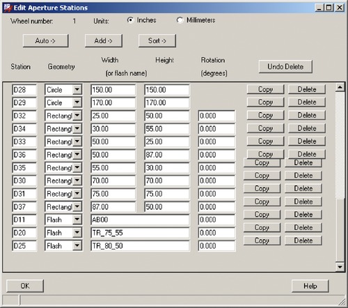 |
| Figure 3-16 Edit Aperture dialog box. |
You should now be familiar with the PCB design flow and PCB Editor tool set. In the following chapters, we look at how to assign footprints to parts from within Capture, how to make your own Capture parts, how to make new footprints with PCB Editor, and how to set up the PCB Editor’s Constraint
Manager to route complex boards.
..................Content has been hidden....................
You can't read the all page of ebook, please click here login for view all page.