Based on an extensive analysis of the wireless communication application domain, in Chapter 2, Ascheid and Meyr propose an architecture description language (ADL) based design flow for ASIPs. While Chapter 4 has elaborated on ADL design issues in detail, in this chapter we focus on advanced software tools required for ADL-based ASIP architecture exploration and design.
The concept of ADL-based ASIP design is sketched in Fig. 16.1. The key is a unique “golden” processor model, described in an ADL, which drives the generation of software (SW) tools as well as hardware (HW) synthesis models. The retargetable SW tools allow us to map the application to the ASIP architecture and to simulate its execution on an architecture virtual prototype. A feedback loop exists to adapt the ADL model (e.g., by adding custom machine instructions to the ASIP) to the demands of the application, based on simulation and profiling results. Another feedback loop back-annotates results from HW synthesis, which allows the incorporation of precise estimations of cycle time, area, and power consumption. In this way, ASIP design can be seen as a stepwise refinement procedure: Starting from a coarse-grain (typically instruction-accurate) model, further processor details are added until we obtain a cycle-accurate model and finally a synthesizable HDL model with the desired quality of results.

This iterative methodology is a widely used ASIP design flow today. One example of a commercial EDA tool suite for ASIP design is CoW-are’s LISATek [1], which comprises efficient techniques for C compiler retargeting, instruction set simulator (ISS) generation, and HDL model generation (see, e.g., [2–4] for detailed descriptions). Another state-of-the-art example is Tensilica’s tool suite, described in Chapter 6 of this book.
While available EDA tools automate many subtasks of ASIP design, it is still largely an interactive flow that allows us to incorporate the designer’s expert knowledge in many stages. The automation of tedious tasks, such as C compiler and simulator retargeting, allows for short design cycles and thereby leaves enough room for human creativity. This is in contrast to a possible pure “ASIP synthesis” flow, which would automatically map the C application to an optimized processor architecture. However, as already emphasized in Chapter 2, such an approach would most likely overshoot the mark, similar to experiences made with behavioral synthesis in the domain of ASIC design.
Nevertheless, further automation in ASIP design is desirable. If the ASIP design starts from scratch, then the only specification initially available to the designer may be the application C source code, and it is far from obvious how a suitable ADL model can be derived from this. Only with an ADL model at hand, the earlier iterative methodology can be executed, and suboptimal decisions in early stages may imply costly architecture exploration cycles in the wrong design subspace. Otherwise, even if ASIP design starts from a partially predefined processor template, the search space for custom (application-specific) instructions may be huge. Partially automating the selection of such instructions, based on early performance and area estimations, would be of great help and would seamlessly fit the above “workbench” approach to ASIP design.
In this chapter we therefore focus on new classes of ASIP design tools, which seamlessly fit the existing well-tried ADL approach and at the same time raise the abstraction level in order to permit higher design productivity.
On one hand, this concerns tools for application source code profiling. A full understanding of the dynamic application code characteristics is a prerequisite for a successful ASIP optimization. Advanced profiling tools can help to obtain this understanding. Profilers bridge the gap from a SW specification to an “educated guess” of an initial HW architecture that can later be refined at the microarchitecture level via the earlier ADL-based design methodology.
Second, we describe a methodology for semiautomatic instruction set customization that utilizes the profiling results. This methodology assumes that there is an extensible instruction set architecture (ISA) and that a speedup of the application execution can be achieved by adding complex, application-specific instruction patterns to the base ISA. The number of potential ISA extensions may be huge, and the proposed methodology helps to reduce the search space by providing a coarse ranking of candidate extensions that deserve further detailed exploration.
The envisioned extended design flow is coarsely sketched in Fig. 16.2. The two major new components are responsible for fine-grained application code profiling and identification of custom instruction candidates. In this way, they assist in the analysis phase of the ASIP design flow, where an initial ADL model needs to be developed for the given application. Selected custom instructions can be synthesized based on a given extensible ADL template model, e.g., a RISC architecture. The initial model generated this way is subsequently further refined within the “traditional” ADL-based flow. Details on the proposed profiling and custom instruction synthesis techniques are given in the following sections.

Designing an ASIP architecture for a given application usually follows the coarse steps shown in Fig. 16.3. First, the algorithm is designed and optimized at a high level. For instance, in the DSP domain, this is frequently performed with block diagram–based tools such as Matlab or SPW. Next, C code is generated from the block diagram or is written manually. This executable specification allows for fast simulation but is usually not optimized for HW or SW design. In fact, this points out a large gap in today’s ASIP design procedures: taking the step from the C specification to a suitable initial processor architecture that can then be refined at the ISA or microarchitecture level. For this fine-grained architecture exploration phase, useful ADL-based tools already exist, but developing the initial ADL model is still a tedious manual process.

Profiling is a key technology to ensure an optimal match between a SW application and the target HW. Naturally, many profiling tools are already available. For instance, Fig. 16.4 shows a snapshot of a typical assembly debugger graphical user interface (GUI). Besides simulation and debug functionality, such tools have embedded profiling capabilities, e.g., for highlighting critical program loops and monitoring instruction execution count. Such assembly-level profilers work at a high accuracy level, and they can even be automatically retargeted from ADL processor models. However, there are two major limitations. First, in spite of advanced ISS techniques, simulation is still much slower than native compilation and execution of C code. Second, and even more important, a detailed ADL processor model needs to be at hand in order to generate an assembly-level profiler. On the other hand, only profiling results can tell what a suitable architecture (and its ADL model) need to look like.

Due to this “chicken-and-egg” problem, assembly-level profiling only is not very helpful in early ASIP design phases.
Profiling can also be performed at the C source code level with tools like GNU gprof. Such tools are extremely helpful for optimizing the application source code itself. However, they show limitations when applied to ASIP design. For example, the gprof profiler generates a table as an output that displays the time spent in the different C functions of the application program and therefore allows identification of the application hot spots. However, the granularity is pretty coarse: a hot-spot C function may comprise hundreds of source code lines, and it is far from obvious what the detailed hot spots are and how their execution could be supported with dedicated machine instructions.
A more fine-grained analysis is possible with code coverage analysis tools like GNU gcov. The output shown in Fig. 16.5 shows pairs of “execution count:line number” for a fragment of an image processing application (corner detection). Now, the execution count per source code line is known. However, the optimal mapping to the ISA level is still not trivial. For instance, the C statement in line 1451 is rather complex and will be translated into a sequence of assembly instructions. In many cases (e.g., implicit type casts and address scaling), the full set of operations is not even visible at the C source code level. Thus, depending on the C programming style, even per–source line profiling may be too coarsely grained for ASIP design purposes. One could perform an analysis of single source lines to determine the amount and type of assembly instructions required. For the previous line 1451, for instance, 5 ADDs, 2 SUBs, and 3 MULs would be required, taking into account the implicit array index scaling. However, in case an optimizing compiler, capable of induction variable elimination, will later be used for code generation, it is likely that 2 MULs will be eliminated again. Thus, while the initial analysis suggested MUL is a key operation in that statement, it becomes clear that pure source level analysis can lead to erroneous profiling results and misleading ISA design decisions.
To overcome the limitations of assembly level and source level profilers, we propose a novel approach called microprofiling (μP). Fig. 16.6 highlights the features of μP versus traditional profiling tools. In fact, μP aims at providing the right profiling technology for ASIP design by combining the best of the two worlds: source-level profiling (machine independence and high speed) and assembly-level profiling (high accuracy).
Table 16.6. Summary of profiler features.
C source level (e.g.gprof) | assembly level (e.g., LISATek) | micro-profiler | |
|---|---|---|---|
primary application | source code optimization | ISA and architecture optimization | ISA and architecture optimization |
needs architectural details | no | yes | no |
speed | high | low | medium |
profiling granularity | coarse | fine | fine |
Fig. 16.7 shows the major components. The C source code is translated into a three address code intermediate representation (IR) as is done in many C compilers. We use the LANCE C frontend [5] for this purpose. A special feature of LANCE, as opposed to other compiler platforms, is that the generated IR is still executable, since it is a subset of ANSI C. On the IR, standard “Dragon Book”–like code optimizations are performed in order to emulate, and predict effects of, optimizations likely to be performed anyway later by the ASIP-specific C compiler. The optimized IR code then is instrumented by inserting probing function calls between the IR statements without altering the program semantics. These functions perform monitoring of different dynamic program characteristics, e.g., operator frequencies. The implementation of the probing functions is statically stored in a profiler library. The IR code is compiled with a host compiler (e.g., gcc) and is linked together with the profiler library to form an executable for the host machine. Execution of the instrumented application program yields a large set of profiling data, stored in XML format, which is finally read via a GUI and is displayed to the user in various chart and table types (see Fig. 16.8).

Simultaneously, the μP GUI serves for project management. The μP accepts any C89 application program together with the corresponding makefiles, making code instrumentation fully transparent for the user. The μP can be run with a variety of profiling options that can be configured through the GUI:
Operator execution frequencies: Execution count for each C operator per C data type, in different functions and globally. This can help designers to decide which functional units should be included in the final architecture.
Occurrences, execution frequencies, and bit width of immediate constants: This allows designers to decide the ideal bit width for integral immediate values and optimal instruction word length.
Conditional branch execution frequencies and average jump lengths: This allows designers to take decisions in finalizing branch support HW (such as branch prediction schemes, length of jump addresses in instruction words, and zero-overhead loops).
Dynamic value ranges of integral C data types: Helps designers to take decisions on data bus, register file, and functional unit bit widths. For example, if the dynamic value range of integers is between 17 and 3,031, then it is more efficient to have 16-bit, rather than 32-bit, register files and functional units.
Apart from these functionalities, the μP can also be used to obtain performance estimations (in terms of cycle count) and execution frequency information for C source lines to detect application hot spots.
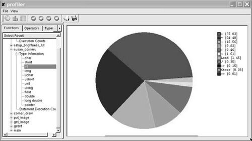
Going back to the previously mentioned image processing example, the μP can first of all generate the same information as gcc, i.e., it identifies the program hot spot at C function granularity. In this example, the hot spot is a single function (“susan_corners”) where almost 100% of the computation time is spent. The μP, however, allows for a more fine-grained analysis: Fig. 16.9 represents a “zoom” into the profile of the hot spot, showing the distribution of computations related to the different C data types. For instance, one can see there is a significant portion of pointer arithmetic, which may justify the inclusion of an address generation unit in the ASIP architecture. On the other hand, it becomes obvious that there are only very few floating point operations, so that an inclusion of an FPU would likely be useless for this type of application.

Fig. 16.10 shows a further “zoom” into the program hot spot, indicating the distribution of C operators for all integer variables inside the “susan_corners” hot spot. One can easily see that the largest fraction of operations is made up by ADD, SUB, and MUL, so that these deserve an efficient HW implementation in the ASIP ISA. On the other hand, there are other types of integer operations, e.g., comparisons, with a much lower dynamic execution frequency. Hence, it may be worthwhile to leave out such machine instructions and to emulate them by other instructions.
The μP approach permits us to obtain such types of information efficiently and without the need for a detailed ADL model. In this way, it can guide the ASIP designer in making early basic decisions on the optimal ASIP ISA. Additionally, as will be described in Section 16.2, the profiling data can be reused for determining optimal ISA extensions by means of complex, application-specific instructions.
In addition to guiding ASIP ISA design, the μP also provides comprehensive memory access profiling capabilities. To make sound decisions on architectural features related to the memory subsystem, a good knowledge of the memory access behavior of the application is necessary. If, for example, memory access profiling reveals that a single data object is accessed heavily throughout the whole program lifetime, then placing it into a scratch-pad memory will be a good choice. Another goal when profiling memory accesses is the estimation of the application’s dynamic memory requirements. As the memory subsystem is one of the most expensive components of embedded systems, fine-tuning it (in terms of size) to the needs of the application can significantly reduce area and power consumption.
The main question in memory access profiling is what operations actually induce memory traffic. At the C source code (or IR) level, there are mainly three types of operations that can cause memory accesses:
Accesses to global or static variables
Accesses to locally declared composite variables (placed on the runtime stack, such as local arrays or structures)
Accesses to (dynamically managed) heap memory
Accesses to local scalar variables usually do not cause traffic to main memory; as in a real RISC-like processor with a general-purpose register bank, scalars are held in registers. Possible, yet rare, memory accesses for local scalar variables can be considered as “noise” and are therefore left out from profiling. As outlined earlier, IR code instrumentation is used as the primary profiling vehicle. In the IR code, memory references are identified by pointer indirection operations. At the time of C to IR translation, a dedicated callback function is inserted before every memory access statement. During execution of the instrumented code, the profiler library searches its data structures and checks whether an accessed address lies in the memory range of either a global variable, a local composite, or an allocated heap memory chunk and updates corresponding read/write counters. In this way, by the end of program execution, all accesses to relevant memory locations are recorded.
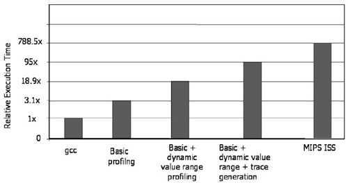
In order to evaluate the μP performance and capabilities, a number of experiments have been performed. The first group of experiments addresses the profiling speed. For fast design space exploration, the μP instrumented code needs to be at least as fast as the ISS of any arbitrary architecture. Preferably, it should be as fast as code generated by the underlying host compiler, such as gcc. Fig. 16.11 compares average speeds of instrumented code versus gcc generated code, and a fast compiled MIPS instruction accurate ISS (generated using CoWare LISATek) for the different configurations of the μP. As can be seen, the speed goals are achieved. The basic profiling options slow down instrumented code execution versus gcc by a factor of only 3. More advanced profiling options increase execution time significantly. However, even in the worst case, the instrumented code is almost an order of magnitude faster than ISS.
Next, we focused on the accuracy of predicting operator execution frequencies. Fig. 16.12 shows the operator count comparisons obtained from a MIPS ISS and instrumented code for the ADPCM benchmark. All the C operators are subdivided into five categories. As can be seen, the average deviation from the real values (as determined by ISS) is very reasonable. These data also emphasize the need to profile with optimized IR code: the average deviation is lower (23%) with IR optimizations enabled than without (36%).

Finally, Fig. 16.13 shows the accuracy of μP-based memory simulation for an ADPCM speech codec with regard to the LISATek on-the-fly memory simulator (integrated into the MIPS ISS). The memory hierarchy in consideration has only one cache level with associativity 1 and a block size of 4 bytes. The miss rates for different cache sizes have been plotted for both memory simulation strategies. As can be seen from the comparison, μP can almost accurately predict the miss rate for different cache sizes. This remains true as long as there is no or little overhead due to standard C library function calls. Since μP does not instrument library functions, the memory accesses inside binary functions remain unprofiled. This limitation can be overcome if the standard library source code is compiled using μP.

The μP has been applied, among others, in an MP3 decoder ASIP case study, where it has been used to identify promising optimizations of an initial RISC-like architecture in order to achieve an efficient implementation. In this scenario, the μP acts as a stand-alone tool for application code analysis and early ASIP architecture specification. Another typical use case is in connection with the ISA extension technology described in Section 16.2, which relies on the profiled operator execution frequencies in order to precisely determine data flow graphs of program hot spots.
Further information on the μP technology can be found in [6]. In [7], a more detailed description of the memory-profiling capabilities is given. Finally, [8] describes the integration of μP into a multiprocessor system-on-chip (MPSoC) design space exploration framework, where the μP performance estimation capabilities are exploited to accurately estimate cycle counts of tasks running on multiple processors, connected by a network on chip, at a high level.
While the μP tool described earlier supports a high-level analysis of the dynamic application characteristics, in this section we focus on the synthesis aspect of ASIPs. Related chapters (e.g., Chapters 6 and 7) in this book emphasize the same problem from different perspectives.
We assume a configurable processor as the underlying platform, i.e., a partially predefined processor template that can be customized toward a specific application by means of ISA extensions. Configurable processors have gained high popularity in the past years, since they take away a large part of the ASIP design risks and allow for reuse of existing IP, tools, and application SW. ISA extensions, or custom instructions, (CIs), are designed to speed up the application execution, at the expense of additional HW overhead, by covering (parts of) the program hot spots with application-specific, complex instruction patterns.
The MIPS32 Pro Series CorExtend technology allows designers to tailor the performance of the MIPS32 CPU for specific applications or application domains while still maintaining the benefits of the industry-standard MIPS32 ISA. This is done by extending the MIPS32 instruction set with custom user-defined instructions (UDIs) with a highly specialized data path.
Traditionally, MIPS provides a complete tool chain consisting of a GNU-based development environment and a specific ISS for all of its processor cores. However, no design flow exists for deciding which instructions should be implemented as UDIs. The user is required to manually identify the UDIs via application profiling on the MIPS32 CPU using classical profiling tools. Critical algorithms are then considered to be implemented using specialized UDIs. The UDIs can enable a significant performance improvement beyond what is achievable with standard MIPS instructions.
These identified UDIs are implemented in a separate block, the CorEx-tend module. The CorExtend module has a well defined pin interface and is tightly coupled to the MIPS32 CPU. The Pro Series family CorExtend capability gives the designer full access to read and write the general-purpose registers, and both single and multiple cycle instructions are supported. As shown in Fig. 16.14 when executing UDIs, the MIPS32 CPU is signaling instruction opcodes to the CorExtend module via the pin interfaces, which are decoded subsequently. The module then signals back to the MIPS32 CPU which MIPS32 CPU resources (for example, register or accumulators) are accessed by the UDI. The CorEx-tend module then has access to the requested resources while executing the UDI. At the end, the result is signaled back to the MIPS32 CPU.
![MIPS CorExtend Architecture (redrawn from [9]).](http://imgdetail.ebookreading.net/hardware/1/9780123695260/9780123695260__customizable-embedded-processors__9780123695260__graphics__f0395-01.jpg)
Further examples of configurable and customizable processors include Tensilica Xtensa, ARCtangent, and CriticalBlue, which are described in more detail in Chapters 6, 8, and 10.
The CorXpert system from CoWare (in its current version) specifically targets the MIPS CorExtend platform. It hides the complexity of the CorExtend RTL signal interface and the MIPSsim CorExtend simulation interface from the designer. The designer is just required to implement the instruction data path using ANSI C for the different pipeline stages of the identified CIs. It utilizes the LISATek processor design technology to automate the generation of the simulator and RTL implementation model. As shown in Fig. 16.15, the CorXpert GUI provides high-level abstraction to hide the complexity of processor specifications. The manually identified CIs are written in ANSI C in the data path editor. Furthermore, the designer can select an appropriate format for the instruction, defining which CPU registers or accumulators are read or written by the instructions. The generated model can then be checked and compiled with a single mouse click. The complete SW tool chain comprising the C compiler, assembler, linker, loader, and the ISS can also be generated by using this GUI.

The problem of identifying ISA extensions is analogous to detecting the clusters of operations in an application that, if implemented as single complex instructions, maximize performance [10]. Such clusters must invariably satisfy some constraints; for instance, they must not have a critical path length greater than that supported by the clock length and the pipeline of the target processor used, and the combined silicon area of these clusters should not exceed the maximum permissible limit specified by the designer. Additionally, a high-quality extended instruction set generation approach needs to obtain results close to those achieved by the experienced designers, particularly for complex applications. So the problem of selecting operations for CIs is reduced to a problem of constrained partitioning of the data flow graph (DFG) of an application hot spot that maximizes execution performance. In other words, CIs are required to be optimally selected to maximize the performance such that all the given constraints are satisfied. The constraints on CIs can be broadly classified in the following categories:
Generic constraints: These constraints are independent of the base processor architecture, but are still necessary for the proper functioning of the instruction set. One of the most important generic constraints is convexity. Convexity means that if any pair of nodes are in a CI, then all the nodes present on any path between the two nodes should also be in the same CI. This constraint is enforced by the fact that, for a CI to be architecturally feasible, all inputs of that CI should be available at the beginning of it and all results should be produced at the end of the same [10]. Thus any cluster of nodes can only be selected as a CI when the cluster is convex. For example, the CIs shown in Fig. 16.16(a) are not convex, since nodes na and nc are present in the same CI (CI1), while the node nb, which lies on the path between na and nc, is in a different CI. The same holds true for the CI2. Thus CI1 and CI2 are both architecturally infeasible.
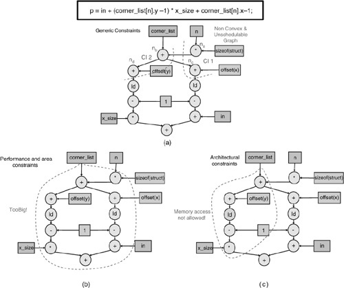
Figure 16.16. Examples of various constraints: (a) generic constraints, (b) performance constraints, (c) architectural constraints. The clusters of operations enclosed within dotted lines represent CIs.
Schedulability is another important generic constraint required for legal CIs. Schedulability means that any pair of CIs in the instruction set should not have cyclic dependence between them. This generic constraint is needed because a particular CI or a subgraph can only be executed when all the predecessors of all the operators in this subgraph are already executed. This is not possible when the operators in different CIs have cyclic dependencies.
Performance constraints: The performance matrices also introduce some constraints on the selection of operators for a CI. Usually embedded processors are required to deliver high performance under tight area and power consumption budgets. This in turn imposes constraints on the amount of HW resources that can be put inside a custom function unit (CFU). Additionally, the critical path length of the identified CIs may also be constrained by such tight budgets or by the architecture of the target processor [11]. Thus, the selection of operators for the CIs may also be constrained by the available area and permissible latencies of a CFU. Fig. 16.16(b) shows an example of the constraints imposed by such area restrictions. The CI obtained in this figure is valid except for the fact that it is too large to be implemented inside a CFU, which has strict area budget.
Architectural constraints: As the name suggests, these constraints are imposed by the architecture itself. The maximum number of general-purpose registers (GPRs) that can be read and written from a CI forms an architectural constraint. Memory accesses from the customized instructions may be not allowed either, because having CIs that access memory creates CFUs with nondeterministic latencies, and the speedup becomes uncertain. This imposes an additional architectural constraint. This is shown in Fig. 16.16(c), where the CI is infeasible due to a memory access within the identified subgraph.
The complexity involved in the identification of CIs can be judged from the fact that, even for such a small graph with only architectural constraints in consideration, obtaining CIs is not trivial. The complexity becomes enormous with the additional consideration of generic and performance constraints during CI identification. Thus, the problem boils down to an optimization problem where the operators are selected to become a part of a CI based on the given constraints.
The proposed CI identification algorithm is applied to a basic block (possibly after performing if-conversion) of an application hot spot. The instructions within a basic block are typically represented as a DFG, G =(N, E), where the nodes N represent operators and the edges E capture the data dependencies between them. A potential CI is defined as a cut C in the graph G such that C ⊆ G. The maximum number of operands of this CI, from or to the GPR file, are limited by the number of register file ports in the underlying core. We denote IN(C) as the number of inputs from the GPR file to the cut C, and OUT(C) as the number of outputs from cut C to the GPR file. Also, let INmax be the maximum allowed inputs from GPR file and OUTmax be the maximum allowed outputs to the same. Additionally, the user can also specify area and the latency constraints for a CI. Now the problem of CI identification can be formally stated as follows:
Problem: Given the DFG G =(N, E) of a basic block and the maximum number of allowed CIs (CImax), find a set S = {C1, C2, ..., CCImax}, that maximizes the speedup achieved for the complete application under the constraints:
∀ Ck ∊ S the condition Ck ⊆ G is satisfied, i.e., all elements of the set S are the subgraphs of the original graph G.
∀ Ck ∊ S the conditions IN(Ck) ≤ INmax and OUT(Ck) ≤ OUTmax are satisfied, i.e., the number of GPR inputs/outputs to a CI does not exceed the maximum limit imposed by the architecture.
∀ Ck ∊ S the condition that Ck is convex is satisfied, i.e., there exists no path from node a ∊ Ck to another node b ∊ Ck through a node w∉Ck.
∀ Ck, Cj ∊ S and j ≠ k the condition thatCk andCj are mutually schedulable is satisfied, i.e., there exists no pair of nodes such that nodes {a, d}∊ Ck and nodes {b, c}∊ Cj where b is dependent on a and d is dependent on c.
∀ Ck ∊ S the condition
 AREA(Ck) ≤ AREAmax is satisfied, i.e., the combined silicon area of CIs does not exceed the maximum permissible value. Here AREA(Ck) represents the area of a particular cut Ck ∊ S.
∀ Ck ∊ S the condition CP(Ck) ≤ LATmax is satisfied, i.e., the critical path, CP(Ck), of any identified CI, Ck, is not greater than the maximum permissible HW latency.
The CIs identified through the solution of this problem are implemented in a CFU tightly attached to the base processor core. The execution of these CIs is usually dependent on the data accessed from the base processor core through GPRs implemented in the same. However, these GPR files usually have a limited number of access ports and thus impose strict constraints on the identification of CIs. Any CI that requires more communication ports than that supported by the GPR file is architecturally infeasible.
Our approach to overcome the restrictions imposed by the architectural constraints of GPR file access is to store the data needed for the execution of an identified CI as well as the outcome of this CI execution, in special registers, termed as internal registers. Such internal registers are assumed to be embedded in the CFU itself. For instance, let us assume that the execution of CI1 in Fig. 16.17 requires five GPR inputs, but the underlying architecture only supports two GPR read ports. This constraint can be overcome with the help of internal registers. A special instruction can be first used to move extra required inputs into these internal registers. Thus, the inputs of nodes nj, nr, and np can be moved from GPRs to internal registers using special move instructions. CI1 can then be executed by accessing five inputs—three from the internal registers and two from the GPRs. Similarly, internal registers can also be used to store the outcomes of CI execution, which cannot be written back to the GPRs directly due to the limited availability of GPR write ports. A special instruction can again be used to move this data back to the GPR in the next cycle. For example, the output of node nj in Fig. 16.17 is moved from an internal register to the GPR with such a special instruction.
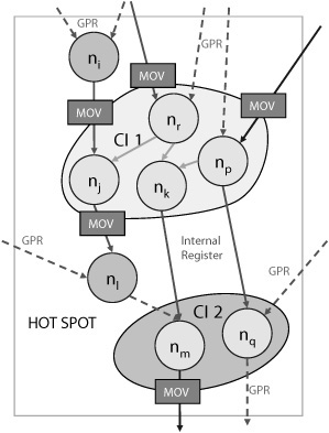
Figure 16.17. Communication via internal registers. Dotted lines represent GPRs, bold lines represent internal registers.
This approach of using internal registers converts an architectural constraint into a design parameter that is flexible and can be optimized based on the target application. More importantly, with this approach the problem stated earlier simplifies to two subproblems:
The first subproblem refers to identification of CIs independent of the architectural constraints imposed by the accessible GPR file ports. The second subproblem refers to the optimal use of the internal registers so that the overhead in terms of area and cycles wasted in moving values from and to these registers is minimized. The resulting instruction set customization problem can be solved in two independent steps as described next.
However, before describing the solutions to these mentioned subproblems, it is important to quantify the communication costs incurred due to the HW cycles wasted in moving the values to and from the internal registers. This can be better understood with the concept of HW and SW domains. All the nodes in clusters, which form the CIs, are implemented in HW in the CFU. As a result these nodes are said to be present in the HW domain. On the other hand, all the nodes of a DFG that are not part of any CI are executed in SW and thus are a part of the SW domain. There can be three possibilities for the use of these internal registers depending on the domains of communicating nodes. These three possibilities together with their communication costs are described here:
A CI can use an internal register to store inputs from the SW domain. This situation is shown in Fig. 16.17, where the node nr receives an input via internal register. The communication between node ni and node nj also falls under this category. In both cases, the loading of internal registers would incur communication cost. This cost depends on the number of GPR inputs allowed in any instruction.
A CI can also use internal registers to provide outputs to the SW domain. This situation is shown in Fig. 16.17, where the node nm produces an output via internal register. The communication between node nj and node nl also falls under this category. In both cases the storing back from internal registers would incur communication cost. As mentioned earlier, this cost depends on the number of GPR outputs allowed in any instruction.
The third possibility of using internal registers is for communicating between two nodes, both of which are in different CIs.[1] This situation does not incur any communication cost, as the value is automatically stored in the communicating internal register after the execution of the producer CI and read by the consumer CI. The communication between nodes nk and nm and the nodes np and nq illustrate this situation. Thus, communication between two CIs with any kind of register (GPR or internal) does not incur any communication overhead.
We use the integer linear programming (ILP) technique to solve the optimization problem described in the previous section. This ILP technique tries to optimize an objective function so that none of the constraints are violated. If the constraints are contradictory and no solution can be obtained, it reports the problem as infeasible.
To keep the computation time within reasonable limits, as a first step all the constraints are considered, except the constraints on the number of inputs and outputs of a CI. However, the objective function in this step does take the penalty of using internal registers into account. The first step optimally decides whether a node remains in SW or forms a part of a CI that is implemented in HW. When this partition of the DFG in HW and SW domain is completed, the algorithm again uses another ILP model in the second step to decide about the means of communication between different nodes. As mentioned before, this communication is possible either through GPRs or through special internal registers. Fig. 16.18 presents the complete algorithm.
Example 16.18. Pseudo code for custom instruction generation.
01        Procedure:InstSetCustomization()
02        Input:
03               DFG= (N,  E  )
04        Output:
05              Identified CIs with registers assigned
06         begin:
07              foreach node  n  ∊  N
08                   if  n cannot be part of CI//e.g n accesses memory
09                             Assign n with  CID=0
10                   else
11                             Assign n with  CID= 1
12                   endif
13             endfor
14
15       STEP 1  :
16            iter=1
17            while  iter   ≤  CI max
18            iter ++
19            // NILP isaset of nodes which are considered while constructing the ILP
20            NILP = Φ
21            foreach node n  ∊  NwithCID <  0
22                  Add n to NILP
23             endfor
24             // Specifytheobjectivefunctionandtheconstraints
25             Develop an ILP problem with NILP
26             if  (Infeasible)
27                     GOTO step2
28             endif
29             Solve the ILP problem
30             foreach node  m  ∊  NILP selected by the solver
31                   Assign CID of m as iter
32             endfor
33          endwhile
34
35       STEP 2  :
36           // EILP isaset of edges which are considered while constructing the ILP
37           EILP= Φ
38           foreach edge  e  ∊  E
39                 if e is an input or output to CI
40                        Add e to EILP
41                 endif
42             endfor
43             // Specify the objective function and the constraints
44             Developan ILP problem with EILP
45             Solve the ILP problem
46             foreach edge b ∊ EILP
47                  if  b is selected by the solver
48                             Assign b as GPR
49                  else
50                             Assign b as internal register
51                  endif
52         endfor
53    end
The algorithm starts with a DFG G =(N, E) of a basic block, where all the nodes are in the SW domain. Each node and each edge is designated with an unique identification (ID) ranging from 1 to |N| and 1 to |E|, respectively. Additionally, each node also has a custom instruction identification (CID), that pertains to the CI that a particular node belongs to. All the nodes in the DFG are initialized with a CID of 0 or – 1 (line 7 to 13 in Fig. 16.18). A value of –1 suggests that the node has the potential of becoming a part of a CI in some iteration. On the other hand, a CID value of 0 suggests that the node can never become a part of any CI. For example, the memory access (LOAD/STORE) nodes may come into this category. Such nodes never take part in any iteration. However, if the node accesses a local scratch-pad memory, it is possible to select this node to form a CI.
The first step of the instruction set customization algorithm is run iteratively over the graph, and in each iteration, exactly one CI is formed (lines 17 to 33). Each node with ID equal to j (written as nj) is associated with a Boolean variable Uj in this step. An iteration counter is additionally used to keep track of the number of iterations (line 16). In each iteration the following sequence of steps is performed.
First, a set NILP = {U 1,U2, ...,Uk}, such that the Boolean variable Ui ∊ NILP if CID of the corresponding node ni is less than 0, is created (lines 21 to 23).
Then an objective function ON where ON = f(U1,U2, ...,Uk), such that Ui ∊ NILP, is specified (line 25).
Next, the constraints on the identification of clusters of nodes to form CIs are represented in form of mathematical inequalities (line 25). Let CN be such an inequality represented by g(U1, U2, ..., Uk) OP const, where g(U1, U2, ..., Uk) is a linear function of Ui ∊ NILP and OP ∊{<, >, ≤, ≥, =}.
If feasible, the ILP solver then tries to maximizeON, ∀Ui ∊ NILP such that all the inequalities CN1, CN2, ..., CNmax are satisfied (line 29). (The maximum number of inequalities depend on the structure of the DFG and the constraints considered.)
When a variableUi has a value of 1 in the solution, the corresponding node ni is assigned with a CID value of the iteration counter. Otherwise, the initialized CID value of node ni is not changed (lines 30 to 32).
The previously mentioned sequence is repeated until the solution becomes infeasible or the maximum bound of CImax is reached. The role of the ILP in each iteration is to select a subgraph to form a CI such that the objective function is maximized under the constraints provided.
The working of step 1 is graphically represented in Fig. 16.19. Parts (b) to (f) of this figure shows the set of associated variables used for specifying the objective function, in iteration one and two, respectively. Moreover, in each iteration all the nodes whose associated variable U is solved for a value of 1 are assigned a CID value of iteration counter, as shown in part (c) and (f). All the other nodes whose associated variable U is solved for a value of 0 are not assigned any new CID but retain their initialized CID values. As a result, all the nodes selected in the same iteration are assigned the same CID, and they form parts of the same CI. Once selected in any iteration, the nodes do not compete with other nodes in subsequent iterations. This reduces the number of variables to be considered by the ILP solver in each iteration. Additionally, the iterative approach makes the complexity independent of the number of CIs to be formed.
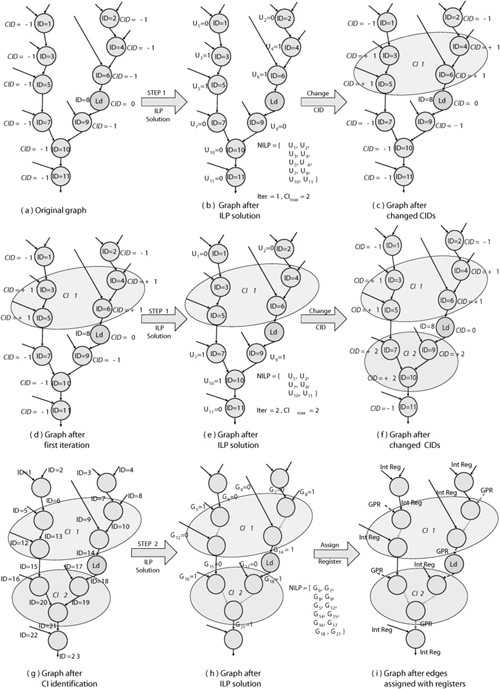
Figure 16.19. Instruction set customization algorithm: (a) original graph, (b), and (c) Step1 CI identification first iteration, (d), (e), and (f) Step1 CI identification second iteration, (g), (h), and (i) Step2 register assignment.
In the second step, the ILP is used to optimally select the GPR inputs and outputs of the CIs. To develop an ILP optimization problem in this step each edge with an ID equal to k (written as ek) is associated with a Boolean variable Gk. This step (lines 35 to 52 in Fig. 16.18) is only executed once at the end of the algorithm in the following sequence:
First, a set EILP = {G1,G2, ...,Gk}, such that the Boolean variable Gi ∊ EILP if the corresponding edge ei is an input to/output from CI, is created (lines 38 to 42).
Then an objective functionOG where OG = f(G1,G2, ...,Gk) such that Gi ∊ EILP is specified (line 44).
Next, the constraints on the GPR inputs/outputs of the CIs are represented in form of mathematical inequalities (line 44). Let CG be such an inequality represented by g(G1, G2, ..., Gk) OP const, where g(G1, G2, ..., Gk) is a linear function of Gi ∊ EILP and OP ∊ { <, >, ≤, ≥, =}.
The ILP solver then tries to maximizeOG, ∀ Gi ∊ EILP such that all the inequalities CG1, CG2,..., CGmax are satisfied (line 45). (The maximum number of inequalities here depend on the number of CIs formed in the first step.)
When a variableGi has a value of 1 in the solution, the corresponding edge ei forms a GPR input/output. On the other hand, if the variable Gi has a value of 0, the edge forms an internal register (lines 46 to 52).
Hence, the complete algorithm works in two steps to obtain CIs and to assign GPR and internal register inputs/outputs to these CIs. The second step is further illustrated in Fig. 16.19(g), (h), and (i). Part (h) shows the set of associated variables used for specifying the objective function and the constraints. The register assignment is shown in part (i).
The previous ISA extension synthesis algorithm completes the envisioned ASIP design flow “on top” of the existing ADL-based flow. The design flow, as shown in Fig. 16.20, can be described as a three-phase process. The first phase consists of application profiling and hot spot detection. The designer is first required to profile and analyze the application with available profiling tools, such as the microprofiler described earlier in this chapter, to determine the computationally intensive code segment known as the application hot spot. The second phase then converts this hot spot to an intermediate representation using a compiler frontend.

This intermediate representation is then used by the CI identification algorithm to automatically identify CIs and to generate the corresponding instruction set extensions in the form of ADL models. The methodology is completely flexible to accommodate specific decisions taken by the designer. For example, if the designer is interested in including particular operators in CIs based on his experience, the CI identification algorithm takes into account (as far as possible) such priorities of the designer. These decisions of the designer are fed to the methodology using an interactive GUI. The third phase allows the automatic generation of complete SW toolkit (compiler, assembler, linker and loader, ISS) and the HW generation of the complete custom processor. This is specifically possible with the use of the ADL-based design flow described at the beginning of this chapter.
The instruction customization algorithm takes the intermediate representation of the C code (as generated by the LANCE compiler front-end [5]) as an input and identifies the CIs under the architectural, generic, and performance constraints. The architectural constraints are obtained from the base processor core, which needs to be specialized with the CFU(s). These constraints are fixed as far as the architecture of the base processor is fixed. The generic constraints are also fixed, as they need to be followed at any cost for the CIs to be physically possible. On the other hand, the performance constraints of chip area and the HW latency are variable and depend on the HW technology and the practical implications. For example, mobile devices have very tight area budgets, which might make the implementation of certain configurations of CFUs practically impossible, despite whatever the speedup achieved may be. Thus the final speedup attained is directly dependent on the amount of chip area permissible or the length of the critical path of the CIs.
The detailed instruction set customization algorithm is therefore run over a set of values with different combinations of area and critical path length to obtain a set of Pareto points. The various SW latency, HW latency, and the HW area values of individual operators are read from an XML file. All the HW latency values and the area values here are obtained with respect to a 32-bit multiplier. For example, a 32-bit (type = “int”) adder would require only 12% of the area required for implementing a 32-bit multiplier. These values are calculated once using the Synopsys Design Compiler and remain the same as far as the simulation library does not change. The XML file can be further extended with the values for 16-bit or 8-bit operations as required by the application source code.
A GUI is provided to steer the instruction set customization algorithm. The GUI acts as a general SW integrated development environment (IDE). Therefore, it provides a file navigation facility, source code browsing, and parameter input facility. Based on the user inputs, the instruction set customization algorithm is run over different values of maximum permissible HW latency and maximum permissible area to obtain Pareto points for these values. The number of Pareto points generated directly depends on the input data provided by the user through the GUI. All the generated Pareto points can viewed in a two-dimensional graph in which the y-axis signifies the estimated speedup and the x-axis signifies the estimated area used in the potential CIs.
A certain cost function is used to estimate the speedup of a potential CI. The speedup can be calculated as the ratio of number of cycles required by a cluster of nodes when executed in SW to that required when executed in HW. In other words, the speedup is the ratio of the SW latency to the HW latency of the potential CI.
Calculation of the SW latency of the cluster is quite straightforward, as it is the summation of the SW latencies of all the nodes included in the cluster.
The calculation of the cycles needed, when an instruction is executed in HW, is much more complicated. Fig. 16.21 illustrates the approach needed for HW cycle estimation for a typical CI. As shown in the figure, the set {n1, n3, n4, n7, n8, n11} forms CI1. Similarly, the sets {n9} and {n14, n15, n6} form parts of CI2 and CI3, respectively. On the other hand, the nodes {n2, n10, n13, n12, n5} are not included in any CI. The nodes that are a part of any CI are present in the HW domain, whereas the nodes that are not the part of any CI are present in the SW domain. Since the nodes in the HW domain can communicate via the internal registers, they do not incur any communication cost. But, when the nodes in HW communicate from (to) the nodes in SW, cycles are needed to load (store) the values. This communication cost can be better understood by considering the example of MIPS32 CorExtend configurable processor, which allows for only two GPR reads from an instruction in a single cycle (only two read ports available). If there are more than two inputs to an instruction like CI1, internal registers can be used to store the extra inputs. And any two operands can be moved into the internal registers in an extra cycle using the two available read ports, given such an architecture. The same processor only allows for a single output from an instruction in a single cycle (only one write port available). So any one operand can be stored back from the instruction using one extra cycle, given such a processor.

Furthermore, the critical path determines the amount of cycles needed for the HW execution of the CI. The critical path is the longest path among the set of paths formed by the accumulated HW latencies of all the operators along that path. For instance in Fig. 16.21 a set of paths, P = {P1, P2, P3, P4} can be created for CI1, where P1 = {n3, n8}, P2 = {n3, n1, n4}, P3 = {n7, n4}, and P4 = {n7, n11}. Assuming that all the operators here individually take the same amount of cycles to be executed in HW, the critical path is P2, since the cumulative HW latencies of nodes along this path are higher than the cumulative HW latencies of nodes along any other path.
If the cycle length of the clock used is greater than this critical path (the operators along the critical path can be executed in single cycle), it is guaranteed that all the other operators in other paths can also be executed within this cycle. This is possible by the execution of all the operators that are not the part of the critical path in parallel by providing appropriate HW resources. For example, in Fig. 16.21 nodes n3 and n7 are not dependent on any other node in CI1 and can be executed in parallel. After their execution, the nodes n8, n1, and n11 can be executed in parallel (assuming all operators have equal HW latencies). Therefore the HW cycles required for the execution of any CI depends on its critical path length.
The HW latency of the cluster can thus be given as the summation of cycles required to execute the operators in critical path (CP) and cycles used in loading (LOAD) and storing (STORE) the operands (using internal registers).
Total HW Latency = CP + LOAD + STORE
The HW latency information of all the operators is obtained by HW synthesis using the Synopsys Design Compiler. This is a coarse-grained approach, as the amount of cycles necessary for the completion of each operator in HW is dependent on the processor architecture and the respective instruction set. Nonetheless, the latency information can be easily configured by using the appropriate library.
The output of the instruction set customization algorithm is a set of solutions that can be viewed on the GUI. The major output of this GUI is in the form of a plot that shows the Pareto points of all the solutions obtained by running the algorithm with different maximum area and latency values. The Pareto curve is shown in Fig. 16.22.
The files of the selected configuration can be saved and the GUI can be used for further interaction. The GUI also displays the solution in the form of a DFG where all the nodes that belong to the same CI are marked with similar colors and boxes. This GUI facility is shown in Fig. 16.23. The complete output consist of the following files:
GDL file contains the contains information on each node and edge of the DFG. This information is used by the GUI to display the graph so that the user can make out which node is a part of which CI.
Modified C source code file contains the source code of the original application with the CIs inserted. This code can then be compiled with the updated SW tool chain.
ADL implementation file contains the behavior code of the CIs in a format that can be used to generate the ADL model of the CFU.
After running the instruction set customization algorithm on the application DFG, each node is assigned a CID that designates the CI to which the node belongs. Additionally, the edges are assigned the register types (internal or GPR). Now for generating the modified C code with CI macros inserted in it, two more steps are to be performed:
First it is required to schedule the nodes, taking into account the dependencies between the same. This step is important to maintain the correctness of the application code. We use a variant of the well known list scheduling algorithm for this purpose.
Another important link missing at this stage of the methodology is the allocation of internal registers. It is worth stating that in the instruction set customization algorithm described earlier, the edges were only assigned with the register types. Now it is required to allocate physical registers to these registers. In our approach, this is performed with a left-edge algorithm known from behavioral synthesis.
The final phase in the instruction set customization design flow is the automatic modification of the SW tools to accommodate new instructions in form of CIs. Additionally, the HW description of the complete CFU(s) that is tightly attached to the base processor core is generated in form of an ADL model. Fig. 16.24 illustrates this for the MIPS CorEx-tend customizable processor core. The region shown within the dotted line is the SW development environment used to design applications for MIPS processors. This environment is updated to accommodate the newly generated CIs using the ADL design flow. The idea is to use the ADL model generated in the second phase of the design process to automatically update the complete SW tool chain.

To hide the complexity of the MIPS CorExtend RTL signal interface and the MIPSsim CorExtend simulation interface [9] from the designer, the CoWare CorXpert tool (see Section 16.2.2) is used. The instruction set customization methodology generates the instruction data path of the identified CIs in a form useable by this tool. CorXpert can then be used to update the SW tool chain and also to generate the RTL model description of the identified CIs. CorXpert utilizes the LISATek processor design technology to automate the generation of the simulator and RTL implementation model. It generates a LISA 2.0 description of the CorExtend module, which can be be exported from the tool for investigation or further modification using the LISATek Processor Designer.
The modified application can thus be compiled using the updated SW tool chain. The updated ISS (MIPSsim in this case) can then be used to obtain the values of real speedup achieved with the generated CIs. The RTL model generated from the ADL model is further synthesized, and the real values of area overhead are obtained. Thus the complete flow starting from the application hot spot down to HW synthesis of the identified CIs is achieved.
This case study deals with the instruction set customization of a MIPS32 CorExtend configurable processor for a specific cryptographic application known as Blowfish. Blowfish [12] is a variable-length key, 64-bit block cipher. It is most suitable for applications where the key does not change often, like a communication link or an automatic file encryptor. The algorithm consists of two parts: data encryption and key expansion. The data encryption occurs via a simple function (termed as the F function), which is iterated 16 times. Each round consists of a key dependent permutation, and a key and data dependent substitution. All operations are XORs and additions on 32-bit words. The only additional operations are four indexed array data lookups per round. On the other hand, the key expansion converts a key of at most 448 bits (variable key-length) into several subkey arrays totaling 4,168 bytes. These keys must be precomputed before any data encryption or decryption. Blowfish uses four 32-bit key-dependent S-boxes, each of which has 256 entries.
The CIs identified for the Blowfish application are implemented in a CFU (CorExtend module), tightly coupled to the MIPS32 base processor core. This processor forces architectural constrains in the form of two inputs from the GPR file and one output to the same. Thus, all the identified CIs must use only two inputs and one output from and to the GPRs. Additionally, the CIs also use internal registers for communication between different CIs. Moreover, the MIPS32 CorExtend architecture does not allow main memory access from the CIs. This places another constraint on the identification of CIs. However, the CorExtend module does allow local scratch-pad memory accesses from the CIs. Later we will show how this facility can be exploited to achieve better speedup. First, the hot spot of Blowfish is determined by profiling. The instruction set customization methodology is then configured for the MIPS32 CorExtend processor core, which provides the architectural constraints for CI identification.
The instruction set customization algorithm is run over the hot spot function of Blowfish. In this case, three CIs are generated. Our methodology also automatically generates the modified source code of the application, with the CIs inserted in it. Fig. 16.25 shows the modified code of the F function after various CIs are identified in it. The modified code is a mixture of three address code and the CIs.
Example 16.25. Blowfish F function: original source code and modified code with CIs inserted.
/****************************************
* Original Code of Function F
***************************************/
externunsignedlong  S[4][256];
unsignedlong F(unsignedlong x)
{
       unsigned short a;
       unsigned short b;
       unsigned short c;
       unsigned short d;
       unsigned long   y;

       d = x & 0x00FF;
       x >>= 8;
       c = x & 0x00FF;
       x >>= 8;
       b = x & 0x00FF;
       x >>= 8;
       a = x & 0x00FF;
       y = S[0][a] + S[1][b];
       y = y ^ S[2][c];
       y = y + S[3][d];

       return y;
}
/****************************************
* Modified Code with CIs inserted
***************************************/
externun signedlongS[4][256];
unsignedlongF(
    unsignedlongx)
{
   int_dummy_RS=1,_dummy_RT=1;
   unsignedlong*t58,*t66,*t84,*t75;
   unsignedlongt85, ldB29C1,ldB28C0;
   unsignedlongldB41C2,ldB53C3;
   //
   //C CodeforBlock 1
   //
   t58 =CI_1 (x,S);
   t66=CI_Unload_Internal(1_dummy_RS,_dummy_RT,3);

   ldB29C1=*/*  load   */t66;
   ldB28C0=*/*  load   */t58;

   t84=CI_2(ldB28C0,ldB29C1);
   t75=CI_Unload_Internal(_dummy_RS,_dummy_RT,5);

   ldB41C2 = */ *load   */t75;
   ldB53C3 = */ *load    */t84;
   t85=CI_3(ldB53C3,ldB41C2);
   return t85;
The automatically generated C behavior code of these CIs is further shown in Figs. 16.26 and 16.27. The term UDI_INTERNAL in this example refers to the internal register file that is implemented in the CFU. This internal register file is represented as an array, in the behavior code, where the index represents the register identifications. The identifiers UDI_RS and UDI_RT and UDI_WRITE_GPR() are MIPS32 CorExtend specific macros and are used to designate the base processor GPRs. UDI_RS and UDI_RT designate the two input GPRs, and the UDI_WRITE_GPR() is used to designate the GPR that stores the result of the CI. The GPR allocation is the responsibility of the MIPS32 compiler. This behavior code is then used by the CorXpert tool to generate the HW description of the CIs.
Example 16.26. Behavior code of CI 1 as implemented in CorXpert.
/************************************
*   Behavior Code of CI 1
***********************************/
    t70 = (uint32)255;
    x = UDI_RS;
    t48 = x >> 8;
    t71 = t48 & t70;
    t72 = (uint16)t71;
    UDI_INTERNAL[2] = t72;
    t61 = (uint32)255;
    t49 = t48 >> 8;
    t62 = t49 & t61;
    t63 = (uint16)t62;
    S = UDI_RT;
    t1 = (uint32)S;
    t60 = 1024 + t1;
    t64 = 4 * t63;
    t65 = t60 + t64;
    t52 = t49 >> 8;
    t66 = (uint32)t65;
    UDI_INTERNAL[3] = t66;
    t78 = 3072 + t1;
    UDI_INTERNAL[4 t78;
    t53 = (uint32)255;
    t54 = t52 & t53;
    t79 = (uint32)255;
    t80 = x & t79;
    t55 = (uint16)t54;
    t81 = (uint16)t80;
    UDI_INTERNAL[1] = t81;
    t56 = 4 * t55;
    t69 = 2048 + t1;
    UDI_INTERNAL[0] = t69;
    t57 = t1 + t56;
    t58 = (uint32)t57;
    UDI_WRITE_GPR(t58);
t78;
t53 = (uint32)255;
t54 = t52 & t53;
t79 = (uint32)255;
t80 = x & t79;
t55 = (uint16)t54;
t81 = (uint16)t80;
UDI_INTERNAL[1] = t81;
t56 = 4 * t55;
t69 = 2048 + t1;
UDI_INTERNAL[0] = t69;
t57 = t1 + t56;
t58 = (uint32)t57;
UDI_WRITE_GPR(t58);Example 16.27. Behavior code of CIs 2 and 3 as implemented in CorXpert.
/********************************
*  Behavior Code of CI 2
********************************
   t72 = UDI_INTERNAL[2];
   t73 = 4 * t72;
   t69 = UDI_INTERNAL[0];
   t74 = t69 + t73;
   t75 = (uint32)t74;
   UDI_INTERNAL[5] = t75;
   ldB28C0 = UDI_RS;
   ldB29C1 = UDI_RT;
   t67 = ldB28C0 + ldB29C1;
   UDI_INTERNAL[6] = t67;
   t81 = UDI_INTERNAL[1];
   t82 = 4 * t81;
   t78 = UDI_INTERNAL[4];
   t83 = t78 + t82;
   t84 = (uint32)t83;
   UDI_WRITE_GPR (t84);

/**********************************
    Behavior Code of CI 3
**********************************/
   t67 = UDI_INTERNAL[6];
   ldB41C2 = UDI_RT;
   t76 = t67 ^ ldB41C2;
   ldB53C3 = UDI_RS;
   t85 = t76 + ldB53C3;
   UDI_WRITE_GPR (t85);
It is worth stating that since MIPS32 has a LOAD/STORE architecture, efficient use of GPRs is very important for achieving optimum performance. The GPR allocation (done by the MIPS32 compiler) directly affects the amount of cycles required for the execution of any CI. Moreover, the most efficient GPR allocation is achieved when the CIs use all the three registers allowed (two for reading and one for writing the results). Hence we use _dummy_ variables in case the CI does not use all the three registers. The use of _dummy_ variables is shown in the example 16.25 in the instruction CI_Unload_Internal.
The modified code, with the CIs inserted, is then run on the MIPS ISS (termed as MIPSsim) to calculate the amount of speedup achieved with the identified CIs. The estimated and the simulated speedup for various configuration of the instruction set customization algorithm is illustrated in Fig. 16.28. A configuration corresponds to the area and latency constraints that the identified CIs need to follow. To get the trend in the speedup, the algorithm was run for various configurations.
Figure 16.28. Speedup for Blowfish hot spot (F) for different algorithm configurations: simulated and estimated. ‘A’ denotes maximum permissible area per CI, and ‘L’ denotes maximum permissible HW latency for CI execution. Both ‘A’ and ‘L’ are specified by the user.
For each such configuration, the algorithm identifies a set of CIs. The speedup obtained by the identified CIs (under the area and latency constraints specified in the configuration) is shown in the figure. For example, A< 200 and L = 2 means that the amount of area per CI should not be greater than 200% (area with respect to 32-bit multiplier) and the CI should be executed within two cycles.[2] It can be seen that the speedup estimation in this case is quite accurate and clearly shows the trend in the amount of speedup achieved for various configuration. The highest simulated speedup achieved is 1.8 times.
The amount of area overhead incurred by the HW implementation of CIs is shown in Fig. 16.29. For obtaining these values, the CorXpert tool was first used to generate the RTL code in Verilog from the behavior code of the CIs. Synopsys Design Compiler was then used for the HW synthesis of the complete CFU.[3] The clock length was set at 5 ns, and the clock constraints were met in all cases. As seen in Fig. 16.29, the area estimation is not as accurate as the speedup estimation. The cost function for area calculation is quite coarsely grained, as it just provides the total area as the sum of individual area of all operators in CIs. The calculated area is more than the estimated area, since we do not consider the area used in the decoding logic in our cost function. However, the estimation does show the trend in the area overhead incurred with different configurations.
Since the Blowfish hot spot contains four memory accesses, the speedup obtained with the identified CIs (without memory accesses) is not too high. To increase the speedup, the lookup tables accessed by the F function can be stored in the local scratch-pad memory and can be accessed from the CIs. These memories are local to the CFU and can be used to store tables and constants that do not require frequent updates. It is useful for the Blowfish application to store the S-Boxes in such scratchpad memories, as they are initialized in the beginning and remain fixed throughout the encryption and decryption process.
Our tool framework provides a facility for the user to specify the scratch-pad memories from different CIs by marking the LOAD node as the SCRATCH accessing node. Each CI shown in the new solution is allowed single scratch-pad memory access (assuming the memory has one read port). The modified source code of the application hot spot is shown in Fig. 16.30. As shown in this example, all the LOADs that were present in Fig. 16.25 are now present inside the CIs. The behavior code of the CIs formed is shown in Figs. 16.31 and 16.32. The variable SCRATCH shown in this example is the scratch-pad memory, implemented as an array in the behavior code.
Example 16.30. Blowfish F function: source code after CI identification (CIs use scratch-pad memories).
/********************************
*   Behavior Code of CI 2
********************************
   t72 = UDI_INTERNAL[2];
   t73 = 4 * t72;
   t69 = UDI_INTERNAL[0];
   t74 = t69 + t73;
   t75 = (uint32)t74;
   UDI_INTERNAL[5] = t75;
   ldB28C0 = UDI_RS;
   ldB29C1 = UDI_RT;
   t67 = ldB28C0 + ldB29C1;
   UDI_INTERNAL[6]=t67;
   t81 = UDI_INTERNAL[1];
   t82 = 4 * t81;
   t78 = UDI_INTERNAL[4];
   t83 = t78 + t82;
   t84 = (uint32)t83;
   UDI_WRITE_GPR (t84);

/**********************************
    Behavior Code of CI 3
**********************************/
    t67 = UDI_INTERNAL[6];
    ldB41C2 = UDI_RT;
    t76 = t67 ^ ldB41C2;
    ldB53C3 = UDI_RS;
    t85 = t76 + ldB53C3;
    UDI_WRITE_GPR (t85);
Example 16.31. Behavior code of CI 1 using scratch-pad memories.
/********************************
*  Behavior Code CI 1
*******************************/
   t70 = (uint32)255;
   x = UDI_RS;
   t48 = x >> 8;
   t71 = t48 & t70;
   t72 = (uint16)t71;
   t73 = 4 * t72;
   t61 = (uint32)255;
   t49 = t48 >> 8;
   t62 = t49 & t61;
   t63 = (uint16)t62;
   UDI_INTERNAL[2] = t63;
   S = 0;
   t1 = (uint32)S;
   UDI_INTERNAL[1] = t1;
   t60 = 1024 + t1;
   UDI_WRITE_GPR (t60);
   t52 = t49 >> 8;
   t78 = 3072 + t1;
   t53 = (uint32) 255;
   t54 = t52 & t53;
   t79 = (uint32)255;
   t80 = x & t79;
   t55 = (uint16)t54;
   UDI_INTERNAL[4] = t55;
   t81 = (uint16)t80;
   t69 = 2048 + t1;
   t74 = t69 + t73;
   t75 = (uint32)t74;
   ldB41C2 = SCRATCH[t75];
   UDI_INTERNAL[3] = ldB41C2;
   t82 = 4 * t81;
   t83 = t78 + t82;
   t84 = (uint32)t83;
   UDI_ INTERNAL[0] = t84;
Example 16.32. Behavior code of CIs 2,3,4 using scratch-pad memories.
/*******************************
*  Behavior Code of CI2
******************************/
    t84 = UDI_INTERNAL[0];
    ldB53C3 = SCRATCH[t84];
    UDI_INTERNAL[5] = ldB53C3;
    t63 = UDI_INTERNAL[2];
    t64 = 4 * t63;
    t60 = UDI_RS;
    t65 = t60 + t64;
    t66 = (uint32)t65;
    UDI_ INTERNAL[6] = t66;
    t55 = UDI_INTERNAL[4];
    t56 = 4 * t55;
    t1 = UDI_INTERNAL[1];
    t57 = t1 + t56;
    t58 = (uint32)t57;
    UDI_WRITE_GPR(t58);

/*********************************
*  Behavior Code of CI 3
********************************/
    t58 = UDI_RS;
    ldB28C0 = SCRATCH[t58];
    ldB29C1 = UDI_RT;
    t67 = ldB28C0 + ldB29C1;
    ldB41C2 = UDI_ INTERNAL[3];
    t76 = t67^ldB41C2;
    ldB53C3 = UDI_ INTERNAL[5];
    t85 = t76 + ldB53C3;
    UDI_WRITE_GPR (t85);

/***********************************
*Behavior  Code of CI_4
**********************************/
   t66 = UDI_INTERNAL[6];
  ldB29C1 = SCRATCH[t66];
  UDI_WRITE_GPR (ldB29C1);
The case study on the Blowfish application has demonstrated the importance of our multiphased methodology with user interaction. The user can typically start from the application source code (written in C) and obtain the description of the customized processor (with enriched instruction set) quickly. With the fully automated approach, the runtime of the instruction set customization algorithm forms the major part of the total time required by the methodology. Since our instruction set customization algorithm can handle moderately large DFGs (approximately 100 nodes) within at most a few CPU minutes, fully customized processor description for moderately sized application hot spots can be achieved within a short time. The case study has further proven the usefulness of user interaction, as the user identifies the scratch-pad memory access by marking the nodes in the DFG of the hot spot. Speedup of the application is considerably increased with the use of these scratch-pad memories.
Moreover, all the other less complex but tedious tasks of modified code generation and ADL model generation have been automated. As a result, the user can experiment with different configurations to obtain results as per the requirements and simultaneously meet the time-to market demand. It is worth mentioning here that the estimated speedup and area are provided for comparison of various solutions. These estimates in no case try to model the absolute values. For modeling the absolute parameters, advanced cost functions and libraries would be required.
The microprofiler and ISA synthesis tools described in this chapter cooperate to support automated ASIP design beyond today’s ADL-based methodology. The microprofiler permits a much more fine-grained type of profiling than existing source-level profilers. Therefore, it meets the demands for optimizing ASIP architectures rather than optimizing source code. At the same time, it does not require a detailed ADL model of the target machine to help in early architecture decisions. The profiling data can be exported for the ISA extension synthesis methodology and tools proposed in this chapter. ISA extension synthesis provides a new level of automation in ASIP design, yet allows for incorporating the designer’s expert knowledge through interaction.
We expect that the demand for such tools (and similar tools as described in various chapters of this book) will increase with the growing availability of reconfigurable processor architectures. The customizable portion of such reconfigurable ASIPs is stored in an embedded FPGA-like HW architecture, which allows for frequent reconfiguration.
For instance, Stretch [13] introduced the S5000 family of processor with a customizable FPGA-based coprocessor and a comprehensive suite of development tools that enable developers to automatically configure and optimize the processor using only their C/C++ code. The S5000 processor chip is powered by the Stretch S5 engine (Fig. 16.33), which incorporates the Tensilica Xtensa RISC processor core and the Stretch instruction set extension fabric (ISEF). The ISEF is a software-configurable datapath based on proprietary programmable logic. Using the ISEF, system, designers extend the processor instruction set and define the new instructions using only their C/C++ code.
![Stretch S5 engine (redrawn from [13]).](http://imgdetail.ebookreading.net/hardware/1/9780123695260/9780123695260__customizable-embedded-processors__9780123695260__graphics__f0422-01.jpg)
Further semiconductor companies will shortly introduce architectures with similar post-fabrication reconfiguration capabilities. For the nonexpert user, use is enabled only via powerful ASIP design tools that (1) help the designer to efficiently and clearly identify what parts of an application to optimize, while (2) abstracting from tedious details on how to implement the necessary HW accelerator configurations.
The author gratefully acknowledges the contributions to the work described in this chapter made by K. Karuri, S. Kraemer, M. Al Faruque, and M. Pandey from the Institute for Integrated Signal Processing Systems at RWTH Aachen University, Germany. Research on the tools described in this chapter has been partially supported by CoWare, Inc., and Tokyo Electron Ltd.
[1] There exists another possibility where nodes within the same CI communicate. In such cases, both nodes are expected to be connected by a HW wire. Hence, this case is not treated here.
[2] The CorExtend module supports a three-stage integer pipeline.
[3] It is assumed here that the constant operands (e.g., 7 is a constant in equation t1= x>> 7) required as the inputs to some CIs are implemented in the CFU itself.