Göran Bilski, Sundararajarao Mohan, and Ralph Wittig
In this chapter we show how certain architectural elements, such as buses, muxes, ALUs, register files, and FIFOs, can be implemented on FPGAs, and the tradeoffs involved in selecting different size parameters for these architectural elements. The speed and area of these implementations dictate whether we choose a bus-based or mux-based processor implementation. The use of lookup tables (LUTs) instead of logic gates implies that some additional logic is free, but beyond a certain point there is a big variation in terms of the speed/area of an implementation. We propose to illustrate all these ideas with examples from the Micro-Blaze implementation. One such example is the FSL interface on Micro-Blaze: we have found that it is better to add a “function accelerator,” with FSL-based inputs and outputs, rather than custom instructions to our soft processor.
This section provides an overview of FPGA architectures and the motivation for building soft processors on FPGAs. FPGAs have evolved from small arrays of programmable logic elements with a sparse mesh of programmable interconnect to large arrays consisting of tens of thousands of programmable logic elements, embedded in a very flexible programmable interconnect fabric. FPGA design and application-specific integrated circuit (ASIC) design have become very similar in terms of methodologies, flows, and the types of designs that can be implemented. FPGAs, however, have the advantage of lower costs and faster time to market, because there is no need to generate masks or wait for the IC to be fabricated. Additional details of FPGAs that distinguish them from ASIC or custom integrated circuits are described next. The rest of this section looks at the background and motivation for creating soft processors and processor accelerators on FPGAs, before introducing the MicroBlaze soft processor in the next section.
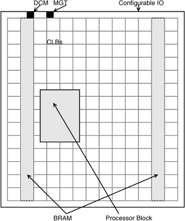
FPGAs have evolved from simple arrays of programmable logic elements connected through switchboxes to complex arrays containing LUTs, block random access memories (BRAMs), and other specialized blocks. For example, Fig. 17.1 shows a high-performance Virtex™-II Pro FPGA, from Xilinx, Inc., containing configurable logic blocks (CLBs) that contain several LUTs, BRAM, configurable input/output blocks, hard processor blocks, digital clock modules (DCMs) and multigigabit transceivers (MGTs).
While the high-performance PowerPC processor block is available in certain members of the Virtex family of FPGAs, it is possible to implement powerful 32-bit microprocessors using the other available resources, such as LUTs and BRAMs, on almost any FPGA. Typical FPGAs contain anywhere from a few thousand 4-input LUTs to a hundred thousand LUTs, and several hundred kilobits to a few megabits of BRAM [1], while a typical soft processor can be implemented with one thousand to two thousand LUTs. Designs implemented on FPGAs can take advantage of special-purpose blocks that are present on the FPGAs (in addition to the basic LUTs).
Fig. 17.2 shows the logic cell in a typical modern FPGA. A 4-input lookup table (4-LUT) can be programmed to implement any logical function of 4 or fewer inputs. The output signal can then be optionally latched or registered. Abundant routing resources are available to interconnect these lookup tables to form almost any desired logic circuit. In addition to the 4-LUT and the output register, various special-purpose circuits are added to the basic cell to speed up commonly used functions, such as multiplexing and addition/subtraction.
Early FPGAs exposed the details of all the routing resources, such as wire segments of various predefined lengths, switch boxes, and connection boxes, to the users so that users could make efficient use of scarce resources. Details of various classical FPGA architectures are described in [2]. Modern FPGAs have abundant routing resources to connect up the logic elements such as LUTs and muxes, and FPGA vendors do not document the interconnect details. Circuit designers typically assume that logic elements placed closer together can be connected together with less delay than logic elements that are placed further apart.
Special-purpose logic implemented on FPGAs from Xilinx or other companies typically includes BRAM (in chunks of several kilobits each), fast carry logic for arithmetic, special muxes, configurable flipflops, LUTs that can be treated as small (16- or 32-bit) RAMs or shift registers, and DSP logic in the form of multiply-accumulate blocks. Any circuit design that targets FPGAs can specifically target a portion of the circuit to these special-purpose blocks to improve speed or area. Synthesis tools that generate circuit implementations from high-level HDL descriptions typically incorporate several techniques to automatically map circuit fragments to these elements, but designers can still achieve significant improvements by manually targeting these elements in specific cases, as described in the subsection “Implementation Specific Details” in Section 17.3.2.
Work on building soft processors in FPGAs has been motivated by two separate considerations. One of the motivations has been the fact that as FPGAs increased in size, it became possible for any FPGA user to define and build a soft processor. Another motivation was the fact that FPGAs were being used by researchers to build hardware accelerators for conventional processors [3]. It was natural to try to combine the processor and the accelerator on the same fabric by building soft processors. Yet another motivation for building soft processors was the desire to aggregate multiple functions on to the same chip. This was the same idea that led ASIC designers to incorporate processors into their designs. As a result of all these different motivations, there is no single application area for soft processors, and soft processors are used wherever FPGAs are used.
In the early 1990s, FPGAs became big enough to support the implementation of small 8-bit or 16-bit processors. At the same time, other FPGA users were creating hardware that was used to accelerate algorithm kernels and loops. The natural combination of these two ideas led to the development of configurable processors, where the instruction set of the processor was tailored to suit the application, and portions of the application were implemented in hardware using the same FPGA fabric. The reconfigurable nature of the FPGA allowed the instruction set itself to be dynamically updated based on the code to be executed. One example of such a processor was the dynamic instruction set computer (DISC) from Brigham Young University [4]. DISC had an instruction set where each instruction was implemented in one row of an FPGA that could be dynamically reconfigured one row at a time. The user program was compiled into a sequence of instructions, and a subset of the instructions needed to start the program was first loaded on to the FPGA. As the program executed on this processor, whenever an instruction was required that was not already loaded, the FPGA was dynamically reconfigured to load the new instruction, replacing another instruction that was no longer required. While this was an interesting concept, practical considerations such as the reconfiguration rates (microseconds to milliseconds), FPGA size limitations, and the lack of caches limited the use of these techniques.
While the potential for implementing custom processors using FPGAs was being explored by various researchers at conferences, such as the FPGA Custom Computing Machines Conference [5] and the International Conference on Field Programmable Logic (FPL) [6], other FPGA users saw the need for standard processors implemented on FPGAs, otherwise known as soft implementations of standard processors. CAST, Inc., described a soft implementation of the 8051 [7], Jan Gray reported his work on implementing a 16-bit processor on a Xilinx FPGA [8], and Ken Chapman reported a small 8/16 bit processor (now known as PicoBlaze) [9]. The key idea in all these implementations was that the processor itself was chosen to be small and simple in order to fit on the FPGAs of the day. Gray, for example, reported that his complete 16-bit processor system required 2 BRAMs, 257 4-LUTs, 71 flipflops, and 130 tristate buffers, and occupied just 16% of the LUT resources of a small SpartanII FPGA. While conventional processors were designed to be built using custom silicon or ASIC fabrication technologies, some of these new soft processors were built for efficient implementation on FPGA fabrics. The KCPSM (now known as PicoBlaze [9]) processor was designed for implementing simple state machines, programmed in assembly language, on FPGAs, while the NIOS family of 16-bit and 32-bit soft processors was designed as a general-purpose processor family [10]. The introduction of the NIOS soft processor family was quickly followed by the introduction of the MicroBlaze soft processor, which is described in detail in the rest of this chapter. Both NIOS and MicroBlaze were general-purpose RISC architectures designed to be used with general-purpose compiler tools and programmed in high-level languages such as C.
While processors (soft or hard) are good at performing general-purpose tasks, many applications contain special tasks that general-purpose processors cannot perform at the required speeds. Classic examples of such tasks are vector computations, floating point calculations, graphics, and multimedia processing. Examples of such applications are the floating point coprocessors that accompanied the early Intel processors, the auxiliary processing unit on the IBM PowerPC [11], and the MMX instructions on the Intel Pentium processors [12]. Coprocessing typically involves the use of a special-purpose interconnect between the main processor and the coprocessor and requires the main processor to recognize certain instructions as coprocessor instructions that are handed off to the auxiliary processor. The complexity of the coprocessor instructions is similar to, or slightly more than, the complexity of the main processor instructions—for example, floating-point-add instead of integer-add.
When researchers started using FPGAs for acceleration of external hard processors, the FPGA-based circuits were much slower than the hardwired processors. Even today, typical soft logic implemented on FPGAs might run at 100 MHz or so, compared to the 400-MHz to 3-GHz clock rates for external processors. To accelerate code running on such a processor using soft logic implemented on an FPGA, the soft logic has to compute the equivalent of more than 4 to 30 processor instructions in 1 clock cycle. As a result, it becomes more attractive to accelerate larger functions or procedures rather than single instructions, so that the communication overhead between the processor and the accelerator is minimized. Starting from the late 1980s researchers have been using FPGAs for function acceleration. A well known early example of FPGA-based function acceleration is the PAM project [3]. Function acceleration is typically implemented over general-purpose buses, shared memories, coprocessor interfaces, or special point-to-point connections such as FSLs (described in more detail in Section 17.3).
Another method to improve application run times is to profile the application and create special-purpose instructions to speed up commonly occurring kernels [13]. While this method has been used successfully for customizable hard processors such as the Tensilica processor, it has not been widely applied to soft processors. While some soft processors such as NIOS allow users to create custom instructions, other soft processors such as MicroBlaze rely on function acceleration, as described in the subsection “Custom Instructions and Function Acceleration” in Section 17.3.2.
MicroBlaze is a 32-bit RISC processor with a Harvard architecture. It has 32 general-purpose registers, and the datapath is 32 bits wide. It supports the IBM standard onchip peripheral bus (OPB). It supports optional caches for data and instructions and multiple FIFO data links known as fast simplex links (FSLs). MicroBlaze has several additional specialized buses or connections, such as the local memory bus (LMB) or the Xilinx cache link (XCL) channels.
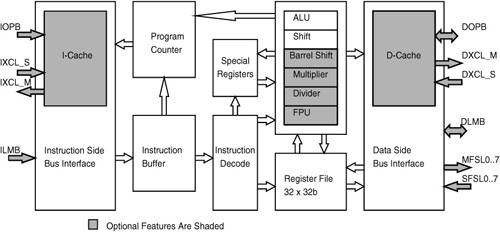
Fig. 17.3 shows the block diagram of MicroBlaze V4.0. The OPB and LMB bus interfaces are shown, along with multiple FSL and XCL interfaces. The optional XCL interfaces are special high-speed interfaces to memory controllers. The other optional elements of MicroBlaze are the barrel shifer, the divider, and the floating point unit (FPU).
MicroBlaze supports a three-operand instruction format. The register file has two read ports and one write port.
MicroBlaze 4.00 has a three-stage pipeline, with the instruction fetch, operand fetch, and the execution stages. At most, one instruction can be in the execute stage at any time. The register file is read during the operand fetch stage and written during the execute stage. While most instructions execute in one cycle, some instructions, such as the hardware multiply, divide, and floating point instruction take multiple cycles to execute. MicroBlaze contains a small instruction prefetch buffer to allow up to four instructions to be prefetched, so the IF stage can be active even when the OF stage is stalled, waiting for the previous instruction to complete execution.
The FPU requires approximately 1,000 LUTs, or almost the area of the basic MicroBlaze processor. The FPU is tightly coupled to the processor and is not a coprocessor or auxiliary processor that resides outside the base processor, and the FPU uses the same general-purpose registers as the other function units, resulting in low latency. The FPU and MicroBlaze run at the same clock frequency. The fact that MicroBlaze is a soft processor allows users to customize the processor, trading off area for performance according to their needs by choosing options such as the FPU. When implemented on a Virtex 4 device, the FPU and Micro-Blaze can run at 200 MHz, to obtain a performance of 33 MFLOPs. The FPU offers a speedup of almost 100 times more than software emulation of floating point instructions, at the cost of doubling the area. Table 17.1 compares the speeds of several floating point instructions on the FPU and in software emulation.
The preceding section described the architecture of MicroBlaze, and highlighted a few performance numbers. While the overall architecture is similar to the basic RISC machines described in textbooks, users can take advantage of the “soft” nature of the processor to create a custom configuration to meet their performance and cost requirements. The tools that allow the user to study these tradeoffs are beyond the scope of this chapter, but it is worth pointing out that standard compiler tools such as gcc are easily adapted to support configurable soft processors.
The basic logic structure in FPGAs is a 4-input LUT that can be programmed to implement any function of 4 or fewer inputs. However, there are several additional structures connected to the LUTs to optimize the implementation of commonly used functions. Some of the notable special structures are:
Dedicated 2-input multiplexers
The outputs of two adjacent LUTs can be multiplexed to implement any 5-input function, or to implement a 4:1 multiplexer, or several other functions with 9 or fewer inputs. These implementations are typically faster and more area efficient than an implementation that uses only LUTs.
A second 2-input MUX allows the output of the functions created in the previous step to be further expanded to implement 8:1 multiplexers, 6-input LUTs, or other functions.
The 4-input LUT is really a 16-bit RAM whose address lines are the same as the LUT inputs. Adjacent LUTs are combined to form dual-ported memories.
The 4-input LUT can also be treated as a cascadable 16-bit shift register.
Dedicated carry logic to implement adderspt
Fast carry chain: A chain of MUXCY elements controlled by the LUT output to either propagate the carry from the previous stage or place a new “generated” carry signal up the chain.
Special XOR gate to compute SUM function: An n-bit adder is implemented using a column of n LUTs controlling n MUXCY elements to generate the carry bits, and n XOR gates to compute the 1-bit sum from the two corresponding input bits and the carry output bit from the previous stage MUXCY.
The carry chain has multiple additional uses for implementing wide functions. Fig. 17.4 shows a wide (12-input) AND function implemented using LUTs and the carry chain. Each 4-input LUT implements a 4-input AND function on 4 of the 12 inputs. Instead of using another LUT to implement a 3-input AND function to build a complete 12-input AND, the output of each LUT is fed to the control input of a 2-input mux that is part of the carry chain. When the output of a LUT is 0, it makes the mux output 0; otherwise, it propagates the value on the right-hand input of the MUXCY element. In this case, the carry chain implements a 3-input AND function without incurring the extra routing and logic delay of an extra LUT stage.

In addition to these logic structures, some larger structures such as dedicated large multipliers and BRAMs are very useful in FPGA applications.
A major difference between ASIC implementations and FPGA implementations of processors is that the area cost in FPGAs is expressed in terms of the number of LUTs, while the area cost in ASICs is expressed in terms of 2-input AND gate implementations. In an ASIC, a 2-input AND gate is much cheaper than a 4-input XOR, which in turn is much cheaper than a 16-bit shift register. In an FPGA, all of these use exactly one LUT and hence cost the same.
Another major difference between ASIC and FPGA implementations is the way the function delay is computed. In ASICs, the delay of a function is dependent on the number of levels of logic in the function, and routing delay plays a negligible role. In FPGAs, the delay of a function is dependent on the number of LUT levels (unless the special structures described earlier are used), and routing delays between LUTs can be a significant part of the total delay.
The essential property of a processor is the instruction set that is supported. When the processor is implemented on an FPGA, the instruction set must match the building blocks of the FPGA logic for efficient implementation. Each LUT performs one bit of a 32-bit operation. MicroBlaze has four logic instructions. The choice of this number is influenced by the fact that a 4-input LUT can process at most four inputs, two of which come from two operands, and two of which select the instruction type. Any fewer than four instructions would result in wasted inputs, and any more than four instructions would require an additional LUT, leading to a doubling of the size.
In silicon-based processor design, the number of pipeline stages is determined by performance and area requirements, and the area or delay cost of a mux is very small compared to the cost of an ALU or other function unit. In FPGA-based soft processor design, the cost of a forwarding or bypass multiplexer is one LUT per bit for a 2-input multiplexer, and this is the same cost as the ALU described in the previous section.
If more pipleline stages are added, the number, the size, and the delay of the required multiplexers increases. The optimal pipeline depth for speed is between three and five, and a deeper pipeline will run slower, negating the benefits of additional pipe stages. The optimal pipeline depth for area is three to four. MicroBlaze 4.00 is optimized for a combination of speed and area with three pipeline stages.
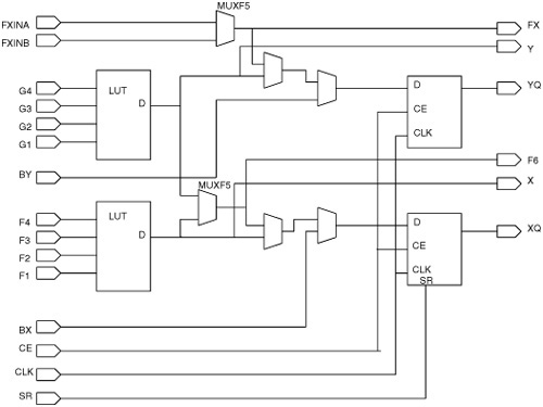
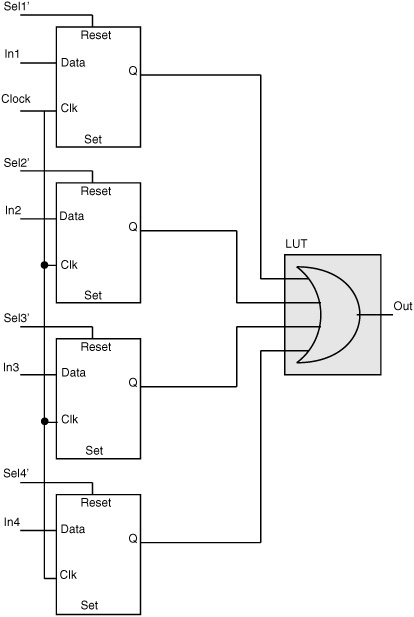
This section describes some specific implementation details of processor modules to take advantage of the FPGA fabric. As a general rule, all timing-critical functions are implemented using the carry chain to reduce logic delays. Wherever possible, the shift register mode of the LUT is used to implement small FIFOs such as FSLs and instruction fetch buffers. Additional set/reset pins on the basic FPGA latch/flip-flop are used to implement additional combinational function inputs, as shown in Fig. 17.5. This figure shows the implementation of a 4-input MUX with fully decoded select inputs. There are four data input signals and four select input signals. Implementing this 8-input function would require more than two 4-LUTs. However, if there are additional unused latches available on the FPGA, the same function can be implemented using four latches and a single 4-LUT as shown. The latch/flipflop elements are configured as transparent latches with the clock signal connected to logic 1. The output of the latch is then equal to the input, unless the reset signal goes to logic 1, causing the output to become logic 0. The inverted form of the select signal is used so each latch implements the AND function of its data input and select input, and at any time exactly one of the four inverted select signals is at logic 0, so that exactly one data input is selected. The latch outputs are combined with an OR function implemented in the 4-LUT to create the 4:1 mux function.
A good example of implementation-based optimization in MicroBlaze is the jump detection logic, where the delay is reduced by two orders of magnitude, from 2 ns, to 0.02 ns, by using carry chains to implement logic.
Fig. 17.6 shows the jump detection logic implemented using two levels of LUTs, with a total delay of 2 ns. The jump signal goes high when a particular 32-bit register contains the value 0 and the opcode corresponds to a jump instruction. The register bits are compared to 0 using LUTs implementing 4-input NOR functions whose outputs are 1 if all four inputs are 0, and 0 otherwise. The carry chain muxes are controlled by these LUT outputs to pass a 1 to the output of the carry chain only if all the LUT outputs are 1. The carry chain output is thus 1 when the register bits correspond to the value 0, and 0 otherwise. Two additional LUTs are used to combine this output called “Reg_is_Zero” with the opcode bits to produce the jump output. The combined delay of the last two cascaded LUTs is 2 ns.

Fig. 17.7 shows how the same circuit is implemented using LUTs and carry logic to reduce the total additional delay to 0.02 ns. The function of the opcode bits and the Reg_is_Zero signal is refactored so that each LUT and the corresponding MULT-AND gate produce an output that is independent of the Reg_is_Zero signal. The first MUXCY mux is used to conditionally select the Reg_is_Zero value or the MULT-AND value, and this result is conditionally propagated through the next MUXCY. Since the LUT outputs are computed independently of Reg_is_Zero, and the LUT inputs are available well before the Reg_is_Zero signal is available, the delay from the time the Reg_is_Zero signal is available to the time the jump signal becomes available is just the propagation time of the carry chain, which is very small (0.02 ns).
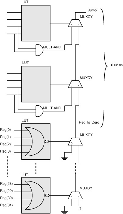
Fig. 17.8 shows a 2-read-port, 1-write-port, 16 × 1 bit register file implemented using the dual-ported RAM building block. Two adjacent 4-LUTs can be configured as a dual-ported 16 × 1 RAM block called the RAM16 X 1D. The RAM16 X 1D block takes two 4-bit addresses labeled as W_ADDR and RD_ADDR. The DPO and SPO outputs correspond to the data stored at the “read address” and “write address,” respectively. The register file uses just the DPO output and ignores the SPO output corresponding to the data stored at the “write address.” The Din input is the data that is written to the register. This building block by itself is not sufficient to implement the actual register file, because three addresses are required, two for read and one for write, and these addresses are all valid in the same clock cycle. Combining two of these blocks with a common write address and write data, and separate read addresses results in a 16 × 1-bit register with two read ports and one write port that can be accessed simultaneously as shown.
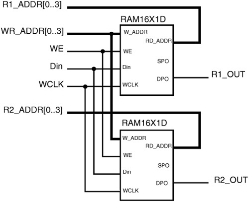
Figure 17.8. 16 × 1-bit Register file with two read ports and one write port implemented using dual-ported LUTRAM building blocks.
In the absence of the 16-bit LUT-RAM blocks, a register file could be implemented using the larger BRAM present on FPGAs. In either case, the number of read/write ports on the register file is limited by the capabilities of the dual-port RAM blocks present on the FPGA. Adding additional ports would require additional muxing and duplication of scarce RAM resources and would slow down the register file itself.
Data sheets published by Xilinx and Altera provide performance numbers for soft processors from these companies. Typically the most advanced, speed-optimized versions of the soft processors run at 100 to 200 MHz on the fastest FPGA devices. Low-cost and low-performance versions of the soft processors run at 50 to 100 MHz on low-cost and low-performance devices from the FPGA manufacturers. These speeds compare with speeds of 1 to 4 GHz for commercial processors from Intel and other vendors, and speeds of 300 to 400 MHz for the hard PowerPC processor in Xilinx FPGAs. The desire to improve the performance of the soft processors leads to the development of custom instructions and function accelerators.
When the processor is implemented as soft logic on an FPGA, and the processor itself can be customized to improve area and performance as described earlier, it is natural to think about adding custom instructions to the processor. Typically, a custom instruction reads and writes the processor registers just like the regular instructions but performs some special function of the data it sees. However, the MicroBlaze implementation has a fixed floor plan to improve performance, and custom instructions disturb this optimal floor plan because it is not possible to allocate a priori, special areas for these functions. Instead of custom instructions, MicroBlaze provides the fast simplex link (FSL) connections and special instructions to read and write FSLs. Micro-Blaze can have up to 32 FSL connections, each consisting of a 32-bit data bus, along with a few control signals to connect function accelerator modules. A function accelerator module can connect to as many FSLs as required. The FSL read/write instructions move data to/from any of the 32 general-purpose registers of MicroBlaze from/to any of the FSL wires. The FSL instructions and wires are predefined so they do not change the area/speed of the processor itself. FSL instructions come in two flavors, blocking and nonblocking. A blocking fsl_read instruction causes the processor to wait until the read data is available, while a nonblocking fsl_read returns immediately. Each FSL connection has a FIFO that allows the function accelerator logic to run at its own speed and perform internal pipelining when possible. The following simple example illustrates how FSLs can be used in function acceleration.
Consider the following code fragment that calls three functions to perform a two-dimensional discrete cosine transform (2D-DCT) function on a two-dimensional array of numbers as follows. The first function call is to a function that performs a one-dimensional discrete cosine transform (1D-DCT) on each row of the two-dimensional array. The second call is to a function that performs a matrix transpose operation, and the third call is to the same 1D-DCT function on each row of the transposed matrix.
/* BEFORE - ALL SOFTWARE*/
  int dct2d (int * array2d) {
    dct1d(array2d);
    transpose(array2d);
    dct1d(array2d);
}
This function can be accelerated by creating a “soft logic” hardware block that performs the entire 2D-DCT function using data that is sent from the processor to the hardware block using the FSL connections on MicroBlaze. The function body for 2D-DCT is replaced by a series of “fsl_write” instructions that transfer data from MicroBlaze registers to the FSL connection called FSL1, followed by a series of “fsl_read” instructions that read the result data back from the hardware using the FSL connection called FSL2.
/* AFTER - HARDWARE ACCELERATED OVER FSL CONNECTION */
  int dct2d (int * array2d) {
      /* write out the array to FSL */
      for (i = 0 to n-1)
        fsl_write(FSL1, array2d[i]);
      for (i = 0 to n-1)
        fsl_read(FSL2, array2d[i]);
    }
The acceleration that can be obtained using this scheme depends on factors such as the relative clock rates of the processor and the accelerator, the number of clock cycles required to send the data to the accelerator, the number of clock cycles used for computing the function in hardware, the number of clock cycles used for computing the function in software, and so on.
While there has been extensive research on generating custom instructions for processors implemented as ASICs [13], there has been some recent interest in custom instructions and function acceleration for soft processors. Jason Cong et al. [14] focus on architectural extensions for soft processors to overcome some of the data bandwidth limitations specific to the FPGA fabric. They describe how the act of placing a custom instruction within the datapath of soft processor can affect the speed of the processor itself, while adding a special link such as the FSL is very useful but is not sufficient by itself to provide a complete solution. While they describe a good solution in terms of shadow registers, this is still an open area for research.
FPGA vendors such as Xilinx [1] and Altera [10] provide tools such as “Xilinx Platform Studio” and “SOPC Builder” to simplify the task of building a processor-based system on FPGAs. The focus of these tools is on describing a processor system at a high level of abstraction, but the tools provide some support for integrating custom instructions and function accelerators with the rest of the hardware. However, the task of identifying and actually implementing the custom instruction or accelerator is left to the system designers. The custom instructions are typically used by programmers writing assembly code or using functional wrappers that invoke assembly code. Designers use standard off-the-shelf compilers, debuggers, and profiling tools. Profiling tools help to identify sections of code that can be replaced with a custom instruction or accelerator.
In this chapter we described how a soft processor is implemented in an FPGA. The architecture of the soft processor is constrained by the FPGA implementation fabric. For example, the number of pipe stages is limited to three in our example, because adding more pipe stages increases the number and the size of multiplexers in the processor, and the relatively high cost of these multiplexers (relative to ASIC implementations) reduces the possible speed advantage. However, these relative costs can change as the FPGA fabric evolves, and new optimizations might be necessary. Several implementation techniques specific to FPGAs were presented to allow designers of soft processors to overcome speed and area limitations. Finally, we pointed out some interesting ideas in extending the processor instruction set and accelerating the soft processor to point out future research areas.