Gerd Ascheid and Heinrich Meyr
We presently observe a paradigm change in designing complex systems-on-chip (SoCs) such as occurs roughly every 12 years due to the exponentially increasing number of transistors on a chip. This paradigm change, as all the previous ones, is characterized by a move to a higher level of abstraction. Instead of thinking in register-transfer level (RTL) blocks and wires, one needs to think in computing elements and interconnect. There are technical issues as well as nontechnical issues associated with this paradigm change. Several competing approaches are discussed in the context of this paradigm change.
The discussion of the pros and cons of these competing approaches is controversial. There are technical as well as nontechnical dimensions to be considered. Even for the technical dimensions, no simple metrics exist. A look at the classic book by Hennessy and Patterson [1] is very instructive. Each chapter closes with sections entitled “fallacy” and “pitfall,” which is an indication that no simple metric exists to characterize a good processor design. This is in contrast to communication engineering. To compare competing transmission techniques, the communication engineers compare the bit rate that can be transmitted over a bandwidth B for a given SNR. Hence, the metric used is bit per second per Hertz bandwidth. A system A is said to be superior to a system B if this metric is larger.
While one might hope that the future brings this metric for the technical dimensions, the case is hopeless with respect to the nontechnical ones. While designing a SoC, the following issues have to be considered:
Risk management
Project management
Time to market
Organizational structure of the company
Investment policy
A design discontinuity has never occurred based on purely rational decisions. Nothing could be farther from reality. Experience has shown that the design discontinuity must be demonstrated with only few engineers. These engineers work on a project with a traditional design methodology and have blown the schedule one time too many. They have two options: the project gets killed or they adopt a new design paradigm.
In our opinion the next design discontinuity will lead to different solutions, depending on the application. We dare to make the following core proposition for wireless communications: future SoC for wireless communications will be heterogeneous, reconfigurable Multi-Processor System-on-Chip (MPSoC).
They will contain computational elements that cover the entire spectrum, from fixed functionality blocks to domain-specific DSPs and general-purpose processors. A key role will be played by ASIPs. ASIPs exploit the full architectural space (memory, interconnect, instruction set, parallelism), so they are optimally matched to a specific task. The heterogeneous computational elements will communicate via a network-on-chip (NoC), as the conventional bus structures do not scale. These MPSoC platforms will be designed by a cross-disciplinary team.
In the following, we will substantiate our proposition. We begin by analyzing the properties of future wireless communication systems and observe that the systems are computationally extremely demanding. Furthermore, they need innovative architectural concepts in order to be energy efficient. We continue by discussing the canonical structure of a digital receiver for wireless communication. In the third part of this chapter, we address the design of ASIPs.
Fig. 2.1 provides an overview of current and future wireless systems.
Today’s communication systems demand very high computational performance and energy-efficient signal processing. Future 4G systems will differ from the existing ones both qualitatively and quantitatively. They will have ultrahigh data rates reaching 1 Gbps, which is multiplexed for densely populated areas to allow mobile Internet services. 4G systems will offer new dimensions of applications. They will be multifunctional and cognitive.
Cognitive radio is defined as an intelligent wireless communication system that is aware of its environment and uses the methodology of understanding by building to learn from the environment and adapt to statistical variations in the input stimuli with two primary objectives in mind: highly reliable communications whenever and wherever needed, and efficient utilization of the radio spectrum, using multiple antennas (MIMO) and exploiting all forms of diversity—spatial, temporal, frequency, and multiuser diversity.
The fundamental tasks to be addressed in the context of cognitive radio are:
Radio scene analysis (e.g., channel estimation, load, capacity, requirements, capabilities)
Resource allocation (e.g., rate power, spectrum, diversity, network elements)
System configuration (e.g., multiple access, coding, modulation, network structure)
The cognitive approach will lead to a new paradigm in the cross-layer design of the communication networks. For example, on the physical layer, the increasing heterogeneity requires flexible coding, modulation, and multiplexing. Current state-of-the-art transmission systems, which are designed for particular sources and channels, may fail in changing conditions. A new flexibility will be introduced: the traditional static design will be replaced by a cognitive approach with, for example, adaptive self-configuration of coding and modulation, taking the instantaneous statistics of the channel and the sources into account.
All these techniques will be introduced with a single objective in mind: to optimally utilize the available bandwidth. It is obvious that these techniques demand ultracomplex signal processing algorithms. The introduction of these complex algorithms has been made economically possible by the enormous progress in semiconductor technology. The communication engineer has learned to trade physical performance measures for signal processing complexity. On top of that, necessary support of legacy systems and multiple (competing) standards further increases processing complexity.
We will discuss in the next section how these algorithms will be processed on a heterogeneous MPSoC, which is designed to find a compromise between the two conflicting objectives of flexibility and energy efficiency. Any MPSoC comprises two dimensions of equal importance, namely processors and interconnects. In this chapter we focus on the processors.
Digital receivers incorporate a variety of functions; basic receiver and transmitter functions include the signal processing of the physical layer, a protocol stack, and a user interface. A cell phone, however, offers an increasing amount of additional functions, such as localization and multimedia applications. Throughout this chapter, physical layer processing is used to make the case, but arguments and concepts apply for the other digital receiver functions as well.
We have discussed in the previous section that the algorithmic complexity of advanced wireless communication systems increases exponentially in order to maximize the channel utilization measured in bps per Hz bandwidth. Until the year 2013, the International Technology Roadmap for Semiconductors (ITRS) estimates an increase of performance requirements by a factor of almost 10,000. Thus, the required computational performance measured in millions of operations per second (MOPS) must increase at least proportionally to the algorithmic complexity, which by far cannot achieved by the standard architectures.
Consequently, there is a need for innovative computer architectures, such as MPSoCs, to achieve the required computational performance at a predicted increase of the clock frequency of a factor of 5 only. However, performance is only one of the drivers for novel architectures. The other is energy efficiency. It is well known that battery energy remains essentially flat. Thus, if the numbers of MOPS must increase exponentially, energy efficiency must grow with at least at the same exponential rate.
We are now confronted with two conflicting goals. On the one hand, one desires to maximize flexibility, which is achieved by a fully programmable processor. However, the energy efficiency of this solution is orders of magnitude too low, as will be demonstrated shortly. Maximum energy efficiency is achieved by a fixed-functionality block with no flexibility at all. A SoC for wireless communications is, therefore, a compromise between these conflicting goals. Conceptually there are two approaches, both of which have been applied to industrial designs. In the first approach, one specifies a maximum energy per task and maximizes flexibility under this constraint. This favors an almost fully programmable solution. In the second approach, one minimizes the hardware flexibility to a constraint set so as to achieve maximum energy efficiency.
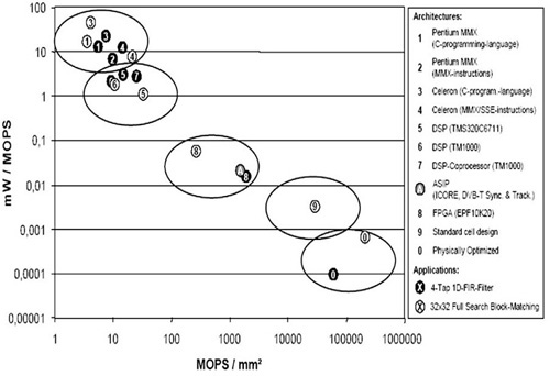
To compare architectures, the useful metrics are area efficiency and energy efficiency. In Fig. 2.2, the reciprocal of energy efficiency measured in mW/MOPS is plotted versus area efficiency measured in MOPS/mm2 for a number of representative signal processing tasks for various architectures.
Source: T. Noll, RWTH Aachen
Figure 2.2. Energy per operation (measured in mW/MOPS) over area efficiency (measured in MOPS/mm2).
The conclusion that can be drawn from this figure is highly interesting. The difference in energy/area efficiency between fixed and programmable functionality blocks is orders of magnitude. An ASIP provides an optimum tradeoff between flexibility and energy efficiency not achievable by standard architectures/extensions.[1]
To assess the potential of complex instructions, as well as the penalty for flexibility expressed in the overhead cost of a processor, we refer to Fig. 2.3, where we have plotted the normalized cost area × time × energy / per sample for various processors and tasks. The numbers differ for other processors; nevertheless, the figure serves well to make the point.[2]
![Normalized cost for execution of sample signal processing algorithms on different processors. Source: [2].](http://imgdetail.ebookreading.net/hardware/1/9780123695260/9780123695260__customizable-embedded-processors__9780123695260__graphics__f0016-01.jpg)
Source: T. Noll, RWTH Aachen
Figure 2.3. Normalized cost for execution of sample signal processing algorithms on different processors. Source: [2].
Let us examine the block-matching algorithm. We see that more than 90 percent of the energy is spent for overhead (flexibility). For other algorithms in this figure, the numbers are even worse. From the same figure we see that the difference in cost between the two DSPs is more than two orders of magnitude. The explanation for this huge difference is simple: the Trimedia has a specialized instruction for the block-matching algorithm, while the TI processor has no such instruction.
While the design space is huge, the obvious question is: can we exploit this gold mine? Before we attempt to outline a methodology to do so, it is instructive to examine Fig. 2.4.
![Number of processing elements (PE) versus issue width per processing element for different network processors. Source: [3].](http://imgdetail.ebookreading.net/hardware/1/9780123695260/9780123695260__customizable-embedded-processors__9780123695260__graphics__f0018-01.jpg)
Figure 2.4. Number of processing elements (PE) versus issue width per processing element for different network processors. Source: [3].
Fig. 2.4 shows network processors based on their approaches toward parallelism. On this chart, we have also plotted iso-curves of designs that issue 8, 16, and 64 instructions per cycle. Given the relatively narrow range of applications for which these processors are targeted, the diversity is puzzling. We conjecture that the diversity of architectures is not based on a diversity of applications but rather a diversity of backgrounds of the architects. This diagram, and the relatively short lives of these architectures, demonstrate that design of programmable platforms and ASIPs is still very much an art based on the design experience of a few experts. We see the following key gaps in current design methodologies that need to be addressed:
Incomplete application characterization: Designs tend to be done with the representative computation kernels and without complete application characterization. Inevitably this leads to a mismatch between expected and delivered performance.
Ad hoc design space definition and exploration: We conjecture that each of the architectures represented in Fig. 2.4 is the result of a relatively narrow definition of the design space to be explored, followed by an ad hoc exploration of the architectures in that space. In other words, the initial definition of the set of architectures to be explored is small and is typically based on the architect’s prior experience. The subsequent exploration, to determine which configuration among the small set of architectures is optimal, is done in completely informal way and performed with little or no tool support.
This clearly demonstrates the need for a methodology and corresponding tool support. In MESCAL, such a methodology is discussed in detail. The factors of the MESCAL methodology [3] are called elements, not steps, because the elements are not sequential. In fact, an ASIP design is a highly concurrent and iterative endeavor. The elements of the MESCAL approach are
Judiciously apply benchmarking
Inclusively identify the architectural space
Efficiently describe and evaluate the ASIPs
Comprehensibly explore the design space
Successfully deploy the ASIP
Element 1 is most often underestimated in industrial projects. Traditionally, the architecture has been defined by the hardware architects based on ad hoc guessing. As a consequence, many of these architectures have been grossly inadequate.
A guiding principle in architecture, which is also applicable to computer architecture, is
Principle: Form follows function. (Mies van der Rohe)
From this principle immediately follows
Principle: First focus on the applications and the constituent algorithms, and not the silicon architecture.
Pitfall: Use a homogeneous multiprocessor architecture and relegate the task mapping to software at the later point in time.
Engineers with a hardware background tend to favor this approach. This approach is reminiscent of early DSP times, when the processor hardware was designed first and the compiler was designed afterward. The resulting compiler-architecture mismatch was the reason for the gross inefficiency of early DSP compilers.
Fallacy: Heterogeneous multiprocessors are far too complex to design and a nightmare to program. We have known that for many years.
This is true in the general case. If, however, the task allows the application of the “divide and conquer” principle, it is not true—as we will demonstrate for the case of a wireless communication receiver.
To understand the architecture of a digital receiver, it is necessary to discuss its functionality. Fig. 2.5 shows the general structure of a digital receiver. The incoming signal is processed in the analog domain and subsequently A/D converted. In this section, we restrict the discussion to the digital part of the receiver.
![Digital receiver structure. Source: [4].](http://imgdetail.ebookreading.net/hardware/1/9780123695260/9780123695260__customizable-embedded-processors__9780123695260__graphics__f0020-01.jpg)
H. Meyr et al., “Digital Communication Receiver”, J.Wiley 1998
Figure 2.5. Digital receiver structure. Source: [4].
We can distinguish two blocks of the receiver called the inner and outer receivers. The outer receiver receives exactly one sample per symbol from the inner receiver. Its task is to retrieve the transmitted information by means of channel and source decoding. The inner receiver has the task of providing a “good” channel to the decoder. As can be seen from Fig. 2.5, two parallel signal paths exist in the inner receiver, namely, detection and parameter estimation path. Any digital receiver employs the principle of synchronized detection. This principle states that in the detection path, the channel parameters estimated from the noisy signal in the parameter estimation path are used as if they were the true values.
Inner and outer receivers differ in a number of key characteristics:
Property of the outer receiver
The algorithms are completely specified by the standards to guarantee interoperability between the terminals. Only the architecture of the decoders is amenable to optimization.
Property of the inner receiver
The parameter estimation algorithms are not specified in the standards. Hence, both architecture and algorithms are amenable to optimization.
The inner receiver is a key building block of any receiver for the following reasons:
Error performance (bit error rate) is critically dependent on the quality of the parameter estimation algorithms.
The overwhelming portion of the receiver signal processing task is dedicated to channel estimation. A smaller (but significant) portion is contributed by the decoders. To maximize energy efficiency, most of the design effort of the digital receiver is spent on the algorithm and architecture design of the inner receiver.
Any definition of a benchmark (element 1 of MESCAL) must be preceded by a detailed analysis of the application. There are several steps involved in this analysis.
The signal processing task can be naturally partitioned into decoders, channel estimators, filters, and so forth. These blocks are loosely coupled. This property allows us to structurally map the task onto different computational elements. The single processing is (almost) periodic. This allows us to temporally assign the tasks by an (almost) periodic scheduler.
Fig. 2.6 is an example of a DVB-S receiver.

The functions to be performed are classified with respect to the structure and the content of their basic algorithmic kernels. This is necessary to define algorithmic kernels that are common to different standards in a multistandard receiver.
Viterbi and MAP decoder
MLSE equalizer
Eigenvalue decomposition (EVD)
Delay acquisition (CDMA)
MIMO Tx processing
Matrix-Matrix and Matrix-Vector Multiplication
MIMO processing (Rx and Tx)
LMMSE channel estimation (OFDM and MIMO)
CORDIC
Frequency offset estimation (e.g., AFC)
OFDM post-FFT synchronization (sampling clock, fine frequency)
FFT and IFFT (spectral processing)
OFDM
Speech post processing (noise suppression)
Image processing (not FFT but DCT)
The cordic algorithm is an efficient way to multiply complex numbers. It is frequently used for frequency and carrier synchronization where complex signals must be rotated by time-varying angles.
The properties of the algorithms must be determined with respect to suitable descriptors.
Since the signal processing task is (almost) periodic, it is instructive to plot complexity (measured in operations per sample) versus the sampling rate; see Fig. 2.7. The iso-curves in such a graph represent MOPS. A given number of MOPS equals the product of
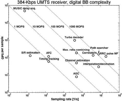
Figure 2.7. Complexity of receiver algorithms (OPS/sample) versus the sampling rate of the processed data.
Operations/sec = (Operations/sample) × (samples/sec)
This trivial but important relation shows that a given number of MOPS can be consumed in different ways: either by a simple algorithm running at a high sampling rate or, conversely, by a complex algorithm running at a low sampling rate. As a consequence, if a set of algorithms is to be processed, then the total amount of MOPS required is a meaningful measure only if the properties of the algorithms are similar. This is not the case in physical layer processing, as illustrated by a typical example.
The first observation to be made from Fig. 2.7 is that the algorithms cover a wide area in the complexity-sampling rate plane. Therefore, the total number of operations per second is an entirely inadequate measure. The algorithms requiring the highest performance are in the right lower quadrant. They comprise of correlation, matched filtering (RRC matched filter), interpolation and decimation, and path searcher to select a number of representative algorithms. But even the algorithms with comparable complexity and sampling rate differ considerably with respect to their properties, as will be demonstrated subsequently.
The correlator and the matched filter belong to a class with similar properties. They have a highly regular data path allowing pipelining, and they operate with very short word lengths of the data samples and the filter coefficients without any noticeable degradation in bit error performance of the receiver [4]. As the energy efficiency of the implementation is directly proportional to the word length, this is of crucial importance. A processor implementation using a 16-bit word length would be hopelessly overdesigned. Interpolation and decimation are realized by a filter with time-varying coefficients for which other design criteria must be observed [4]. The turbo-decoder is one of the most difficult blocks to design with entirely different algorithmic properties than the matched filter or the correlator discussed earlier. Of particular importance is the design of the memory architecture. A huge collection of literature on the implementation of this algorithm exists. We refer the reader to [5–8] and to Chapter 17 of this book.
As an example of a complex algorithm running at low sampling rate (left upper corner), we mention the MUSIC algorithm, which is based on the Eigenvalue decomposition.
As a general rule for the classification of the baseband algorithm, we observe from Fig. 2.7 that the sampling rate decreases with increasing “intelligence” of the algorithms. This is explained by the fact that the number crunchers of the right lower corner produce the raw data that is processed in the intelligent units tracking the time variations of the channel. Since the time variations of the channel are only a very small fraction of the data transmission rate, this can be advantageously exploited for implementation.
In summary, the example has demonstrated the heterogeneity of the algorithms. Since the complete task can be separated into subtasks with simple interconnections, it can be implemented as a heterogenous MPSoC controlled by a predefined, almost periodic scheduler.
The findings are identical to the one of the previous example. Due to the much higher data rate of 200 Mbps, the highest iso-curve is shifted toward 100 GOPS.
An analogous analysis has been published by L. G. Chen in [9].
Extensive use of parallelism is the key to achieving the required high throughputs, even with the moderate clock frequencies used typically in mobile terminals. On the top level there is, of course, the task level parallelism by parallel execution of the different applications. This leads to the heterogenous MPSoC, as discussed before. But even the individual subtasks of the physical layer processing can often be executed in parallel when there is a clear separation between the subtasks, as suggested by the block diagram of the DVB-S receiver shown in Fig. 2.6.
For the individual application-specific processor, all known parallelism approaches have to be considered and may be used as appropriate. Besides the parallel execution by pipelining, the most useful types of instruction parallelism are: very long instruction word (VLIW), single instruction multiple data (SIMD), and complex instructions. Within instruction parallelism, VLIW is the most flexible approach, while the use of complex instructions is the most application-specific approach.
Since each of these approaches has specific advantages and disadvantages, a thorough exploitation of the design space is necessary to find the optimum solution. VLIW (i.e., the ability to issue several individual instructions in parallel as a single “long” instruction) inherently introduces more overhead (e.g., in instruction decoding) but allows parallel execution even when the processing is less regular. With SIMD, there is less control overhead, since the same operation is performed on multiple data, but for the same reason it is only applicable when the processing has significant regular sections.[3] Finally, grouping several operations into a single, complex instruction is very closely tied to a specific algorithm and, therefore, the least flexible approach. The main advantage is its efficiency, as overhead and data transfer is minimized.
As discussed in the previous section, the algorithms in the lower right corner of Fig. 2.7 are number crunchers, where the same operations are applied to large amounts of data (since the data rate is high). For these algorithms, SIMD and complex instructions are very effective. More “intelligent” algorithms, which are found in the upper part of the diagram, are by definition more irregular. Therefore, VLIW typically is more effective than the other two approaches here.
Since the key measures for optimization are area, throughput, and energy consumption, exploitation of parallelism requires a comparison not only on the instruction level but also on the implementation level. For example, a complex instruction reduces the instruction count for the execution of a task but may require an increased clock cycle (i.e., reduce the maximum clock frequency).
The design of a processor is a very demanding task, which comprises the design of the instruction set, micro architecture, RTL, and compiler (see Fig. 2.8). It requires powerful tools, such as a simulator, an assembler, a linker, and a compiler. These tools are expensive to develop and costly to maintain.

In traditional processor development, the design phases were processed sequentially as shown next. Key issues of this design flow are the following:
Handwriting fast simulators is tedious, prone to error and difficult.
Compilers cannot be considered in the architecture definition cycle.
Architectural optimization on RTL is time consuming.
Likely inconsistencies exist between tools and models.
Verification, software development, and SoC integration occur too late in the design cycle. Performance bottlenecks may be revealed in this phase only.
This makes such a design flow clearly unacceptable today.
We conjectured earlier that future SoCs will be built largely using ASIPs. This implies that the processor designer team will be different, both quantitatively and qualitatively, from today. As the processors become application-specific, the group of designers will become larger, and the processors will be designed by cross-disciplinary teams to capture the expertise of the domain specialist, the computer architect, the compiler designer, and the hardware engineer. In our opinion, it is a gross misconception of reality to believe that ASIPs will be automatically derived from C-code provided by the application programmer.

The paradigm change (think in terms of processors and interconnects) requires a radically different conception of how and by whom the designs will be done in the future. In addition, it requires a tool suite to support the design paradigm, as will be discussed in the next section.
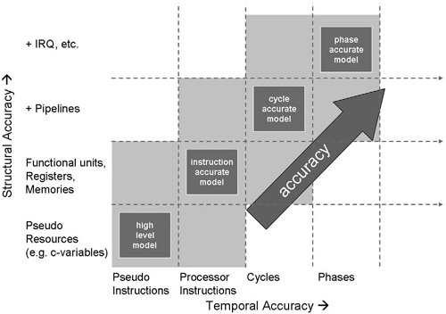
In our view, the key enabler to move up to a higher level of abstraction is an architecture description language (ADL) that allows the modeling of a processor at various levels of structural and temporal accuracy.
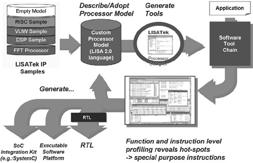
From the LISA2.0 description:[4]
The software (SW) tools (assembler, linker, simulator, C compiler) are fully automatically generated.
A path leads to automatic hardware (HW) implementation. An intermediate format allows user-directed optimization and subsequent RTL generation.
Verification is assisted by automatic test pattern generation and assertion-based verification techniques [10].
An executable SW platform for application development is generated.
A seamless integration into a system simulation environment is provided, thus enabling virtual prototyping.
This is illustrated in Fig. 2.11.

We like to compare the LISATek tool suite with a workbench. It helps the designer efficiently design a processor and integrate the design into a system-level design environment for virtual prototyping. It does not make a futile attempt to automate the creative part of the design process. Automation will be discussed next.
A few general comments about automation appear to be in order. We start with the trivial observation: design automation per se is of no value. It must be judged by the economic value it provides.
Fallacy: Automate to the highest possible degree
Having conducted and directed academic design tools research that led to commercially successful products over many years[5], we believe that one of the worst mistakes of the academic community is to believe that fully automated tools are the highest intellectual achievement. The companions of this belief in the EDA industry are highly exaggerated claims of what the tools can do. This greatly hinders the acceptance of a design discontinuity in industry, because it creates disappointed users burned by the bad experience of a failed project.
Principle: You can only automate a task for which a mathematical cost function can be defined
The existence of a mathematical cost function is necessary to find an optimum. Finding the minimum of the cost function is achieved by using advanced mathematical algorithms. This is understood by the term automation. Most often, finding an optimum with respect to a given cost function requires human interaction. As an example, we mention logic synthesis and the tool design compiler.
Pitfall: Try to automate creativity
This is impossible today and in the foreseeable future. It is our experience, based on real-world designs, that this misconception is based on a profound lack of practical experience, quite often accompanied by disrespect for the creativity of the design engineer. By hypothetically assuming that a “genie approach” works, it is by no means clear what the economic advantage of this approach would be, compared to an approach where the creative part of a design is left to an engineer supported by a “workbench.” The workbench performs the tedious, time-consuming, and error-prone tasks that can be automated.
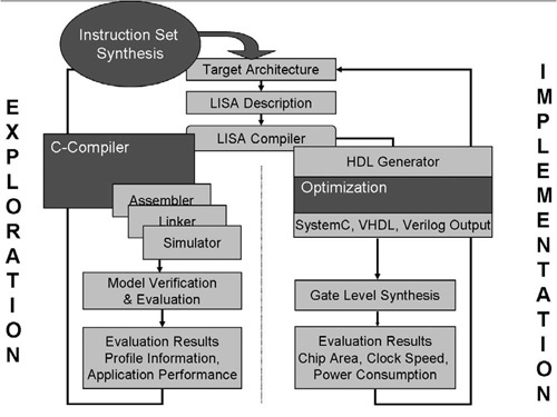
The LISATek tool suite follows the principles of a workbench. The closed loop shown in Fig. 2.12 is fully automated: from the LISA2.0 description, the SW tools are automatically generated.
In the exploration phase, the performance of the architecture under investigation is measured using powerful profiling tools to identify hot-spots. Based on the result, the designer modifies the LISA2.0 model of the architecture, and the software tools for the new architecture variant are generated in a few seconds by a simple key stroke. This rapid modeling and retargetable simulation and code generation allow us to iteratively perform a joint optimization of application and architecture. In our opinion, this fully automatic closed loop contributes most to the design efficiency. It is important to emphasize that we keep the expert in the loop.
A workbench must be open to attach tools that assist the expert in his search for an optimum solution. Such optimization tools are currently a hot area of research [11–17] in academia and industry. It is thus of utmost importance to keep the workbench open to include the result of this research. To achieve this goal, we have strictly followed the principle of orthogonalization of concerns: any architecture optimization is under the control of the user. Experience over the years with attempts to hide optimization from the user has shown to be a red herring, since it works optimally only in a few isolated cases (which the tool architect had in mind when he crafted the tool) but leads to entirely unsatisfactory results in most other cases.
For example, a tool that analyzes the C-code to identify patterns suitable for the fusion of operations (instruction set synthesis) leading to complex instruction is of the greatest interest. Current state of the art includes the Tensilica XPRES tool, the instruction-set generation developed at the EPFL [18, 19], and the microprofiling technique [20] developed at the ISS. All these tools allow the exploration of a large number of alternatives automatically, thus greatly increasing the design efficiency.
However, it would be entirely erroneous to believe that these tools automatically find the “best” architecture. This would imply that such a tool optimally combines all forms of parallelization (instruction level, data level, fused operations), which is clearly not feasible today. C-code as the starting point for the architecture exploration provides only an ambiguous specification. We highly recommend reading the paper of Ingrid Verbauwhede [21], in which various architectural alternatives of an implementation of the Rijndahl encryption algorithm based on the C-code specification are discussed.
Rather, these instruction set synthesis tools are analysis tools. Based on a given base architecture, a large number of alternatives are evaluated with respect to area and performance to customize the architecture. The results of this search are given in form of Pareto curves (see Chapter 6). In contrast to an analysis tool a true synthesis tool would deliver the structure as well as the parameters of the architecture. For a detailed discussion, the reader is referred to Chapter 7.
Once the architecture has been specified, the LISATek workbench offers a path to hardware implementation. The RTL code is generated fully automatically. As one can see in Fig. 2.13, the implementation path contains a block labelled “optimization.” In this block, user-controlled optimizations are performed to obtain an efficient hardware implementation. The optimization algorithms exploit the high-level architectural information available in LISA; see [22–24] for more detail.
While it is undisputed that the design of an ASIP is a cross-disciplinary task that requires in-depth knowledge of various engineering disciplines—algorithm design, computer architecture, HW designs—the conclusion to be drawn from this fact differs fundamentally within the community. One group favors an approach that in its extreme implies that the application programmer customizes a processor, which is then automatically synthesized. This ignores the key fact (among others) that architecture and algorithm must be jointly optimized to get the best results.
Numerous implementations of the algorithm are available in the literature. The cached FFT algorithm is instructive because of its structure. The structure allows the exploitation of data locality for higher energy efficiency, because a data cache can be employed. On the architecture side, the ASIP designer can select the type and size of the data cache. The selection reflects a tradeoff between the cost of the design (gate count) and its energy efficiency. On the algorithm side, a designer can alter the structure of the algorithm, for instance, by changing the size of the groups and the number of epochs. This influences how efficiently the cache can be utilized for a given implementation. In turn, possible structural alterations are constrained by the cache size. Therefore, a good tradeoff can only be achieved through a joint architecture/algorithm optimization, through a designer who is assisted by a workbench. No mathematical optimization will find this best solution, because there is no mathematical cost function to optimize. For the final architecture, RTL code will be automatically generated and verified and, subsequently, optimized by the hardware designer.
Fallacy: The cross-disciplinary approach is too costly
This conjecture is supported by no practical data. The contrary is true, as evidenced by successful projects in industry. As we have discussed earlier, one of the most common mistakes made in the ASIP design is to spend too little effort in analyzing the problem and benchmarking (element 1 of the MESCAL methodology); see [3]. The design efficiency is only marginally affected by minimizing the time spent on this task, at the expense of a potentially grossly suboptimal solution. The overwhelming improvement of design efficiency results from the workbench.
However, the cross-disciplinary project approach today is still not widespread in industry. Why is this? There are no technical reasons. The answer is that building and managing a cross-disciplinary team is a very demanding task. Traditionally, the different engineering teams involved in the different parts of a system design have had very little interaction. There have been good reasons for this in the past when the tasks involved could be processed sequentially, and thus the various departments involved could be managed separately with clearly defined deliverables. For today’s SoC design, however, this approach is no longer feasible.
Budgets and personnel of the departments need to be reallocated. For example, more SW engineers than HW designers are needed. However, any such change is fiercely fought by the departments that lose resources. Today the formation of a cross-disciplinary team takes place only when a project is in trouble.
Finally we need to understand that in a cross-disciplinary project, the whole is more than the sum of the parts. In other words, if there exist strong interactions between the various centers of gravity, decisions are made across disciplinary boundaries. Implementing and managing this interaction is difficult. Why? Human nature plays the key role. Interaction between disciplines implies that no party has complete understanding of the subject. We know of no engineer, including ourselves, that gladly acknowledges that he does not fully understands all the details of a problem. It takes considerable time and discipline to implement a culture that supports cross-disciplinary projects, whether in industry or academia.
We conjecture that in the future, mastering a cross-disciplinary task will become a key asset of the successful companies. Cross-discipline goes far beyond processor design. This has been emphasized in a talk by Lisa Su [25] about the lessons learned in the IBM CELL processor project. Su also made the key observation that in the past, performance gain was due to scaling, while today pure scaling contributes an increasingly smaller portion to the performance gain (Fig. 2.14).
![Gain by scaling versus gain by innovation [25].](http://imgdetail.ebookreading.net/hardware/1/9780123695260/9780123695260__customizable-embedded-processors__9780123695260__graphics__f0034-01.jpg)
Source: Lisa Su/IBM: MPSoC 05 Conference 2005
Figure 2.14. Gain by scaling versus gain by innovation [25].
Integration over the entire stack, from semiconductor technology to end-user applications, will replace scaling as the major driver of increased system performance. This corroborates the phrase “design competence rules the world.”
In Fig. 2.16 we have summarized the evolution of processor applications in wireless communication. In the past we have found a combination of general-purpose RISC processors, digital signal processors, and fixed wired logic. Today, the processor classes have been augmented by the class of configurable and scalable processors. In the future an increasing number of true ASIPs exploiting all forms of parallelism will coexist with the other classes.
![Future improvements in system performance will require an integrated design approach [25].](http://imgdetail.ebookreading.net/hardware/1/9780123695260/9780123695260__customizable-embedded-processors__9780123695260__graphics__f0036-01.jpg)
Figure 2.15. Future improvements in system performance will require an integrated design approach [25].

The key question is, what class of architecture is used where? As a general rule, if the application comprises large C-programs such as in multimedia, the benefit of customization and scalability might be small. Since the processor is used by a large number of application programmers with differing priorities and preferences, optimization will be done by highly efficient and advanced compiler techniques, rather than architectural optimization. The application is not narrow enough to warrant highly specialized architectural features. For this class a domain-specific processor is probably the most economical solution.
Configurable (customizable) processors will find application when the fairly complex base architecture is justified by the application and, for example, when a customized data path (complex instruction) brings a large performance gain. Advantages of a customized processor are the minimization of the design risk (since the processors is verified) and the minimization of design effort.
The class of full ASIPs offers a number of key advantages, which go far beyond instruction-set extensions. The class includes, for example, application-specific memory and interconnect design. Technically, exploiting the full architectural options allows us to find an optimum tradeoff between energy efficiency and flexibility. If the key performance metric is energy efficiency, then the flexibility must be minimized (“just enough flexibility as required”). In the case of the inner receiver (see Fig. 2.5), most functionality is described by relatively small programs done by domain specialists. For these applications, a highly specialized ASIP with complex instructions is perfectly suited. Quite frequently, programming is done in assembly, since the number of lines of code is small (see for example: [26] and [27]).
Economically, the key advantage of the full ASIP is the fact that no royalty or license fee has to be paid. This can be a decisive factor for extremely cost-sensitive applications with simple functionality for which a streamlined ASIP is sufficient. Also, it is possible to develop a more powerful ASIP leveraging existing software by backward compatibility on the assembler level. For example, in a case study a pipelined micro-controller with 16/32-bit instruction encoding was designed, which was assembler-level compatible with the Motorola 68HC11. The new micro-controller achieved three times the throughput and allowed full reuse of existing assembler code.
Finally, we should also mention that most likely in the future processor processors will have some degree of reconfigurability in the field. This class of processors can be referred as reconfigurable ASIPs (rASIPs). In wireless communication application, this post-fabrication flexibility will become essential for software-configurable radios, where both a high degree of flexibility and high performance are desired. Current rASIP design methodology strongly relies on the designer expertise without the support of a sophisticated workbench (like LISATek). Consequently, the design decisions, like amount of reconfigurability, processing elements in the reconfigurable block, or the processor-FPGA interface, are purely based on designer expertise. At this point, it will be interesting to have a workbench to support the designer taking processor design decisions for rASIP design.
[1] The data point A is included for qualitative demonstration only, as it performs a different task.
[2] By “first instantiation,” it is understood that the processor performs only one task. By “free computational resource,” it is understood that the processor has resources left to perform the task. The latter is a measure for the useful energy spent on the task. The difference between “first instantiation” and “free computational resources” is the penalty paid for flexibility [2].
[3] The term “regular sections” here denotes sections where a particular sequence of arithmetic operations is applied to multiple data.
[4] The ADL language LISA2.0, which is the base of the LISATek tool suite of CoWare, was developed at the Institute for Integrated Signal Processing Systems (ISS) of RWTH Aachen University. The LISATek tool suite is described in an overview in the book, where further technical references can be found. For this reason we do not duplicate the technical details of LISATek here.
[5] The toolsuite COSSAP was also conceived at ISS of RWTH Aachen University. It was commercialized by the start-up Cadis, which the authors of this chapter co-founded. Cadis was acquired in 1994 by Synopsys. COSSAP has been further developed into the “Co-Centric System Studio” Product. The LISATek tool suite was also conceived at ISS. It was commercialized by the start-up LISATek, which was acquired by CoWare in 2003.