
8: Systems on a chip
Abstract
This chapter examines embedded systems built entirely within one chip, which is typically a field-programmable gate array (FPGA). The primary objective of the chapter is to examine the architecture of FPGAs and the tools that enable a designer to find and fix design problems within the hardware or software, or both.
Keywords
SoC; FPGA; Tilera; Logic analyzer; Xilinx; MicroBlaze; Terasic; Stratix; Agilex; Lauterbach
Introduction
When we refer to a system on a chip (SoC) or a system on silicon (SoS), we are simply acknowledging that when you have the ability to place one or more CPU cores on a silicon die and also place RAM, nonvolatile memory, peripheral devices, etc., on that same die, you’ve built a system. If that silicon die happens to be a field-programmable gate array (FPGA) with an embedded CPU, such as an ARM, core, then you have a reconfigurable system on a chip.
Debugging such a system provides some unique challenges, primarily the lack of internal visibility. This means that we have to depend more upon simulation tools as well as an on-chip debug core to substitute for our inability to connect a logic analyzer to the internal buses.
Another challenge is that designers can put multiple cores on one die and come up with devilishly clever ways to interconnect them to share the workload for maximum efficiency. Unfortunately, the tighter the coupling between the processors, the more difficult it will be to sort them out.
Quite a while ago, I attended one of the annual Microprocessor Forums in Silicon Valley. I recall that one presentera related that his company can design an ASIC with 64 32-bit RISC processors on it and they have no idea how to debug it.
Fast forward. I just watched a YouTube video of the Tilera GX-72 SoC with 72 64-bit cores [1]. In disbelief, I went to the company’s website and found this introductory blurb,
The TILE-Gx72™ Processor is optimized for intelligent networking, multimedia, and cloud applications, and delivers remarkable computing and I/O with complete “system-on-a-chip” features. The device includes 72 identical processor cores (tiles) interconnected with the iMesh™ on-chip network. Each tile consists of a full-featured, 64-bit processor core as well as L1 and L2 cache and a non-blocking Terabit/sec switch that connects the tiles to the mesh and provides full cache coherence among all the cores. [2]
Wow! I’d love to see what one of those chips could do running the thermostat in my home.
I was a member of the R&D team at Hewlett-Packard’s Logic Systems Division in Colorado Springs, Colorado, that developed HP’s 64700 family of in-circuit emulators. This emulator family was a departure from the standalone workstation design of the original HP 64000 because the host computer was a personal computer, linked to the emulator over an RS-232 or RS-422 serial connection.
We received a patentb for a feature we added called the CMB, or the Coordinated Measurement Bus. The CMB was added because we could see that debugging systems containing multiple microprocessors would become an issue that would need to be addressed by the embedded tool vendors as the technology evolved.
The CMB enabled multiple emulators to cross-trigger their internal trace analyzers as well as start together and cross-trigger breakpoints. I thought it was a pretty neat feature until we actually tried to use it. The problem was not the technology, which really worked well. We discovered that after we had more than two emulators linked together, trying to wrap our minds around what was happening became exponentially more difficult. I suspect that our customers had a similar problem.
I mention this because in this chapter we’ll look at debugging integrated circuits containing multiple CPU cores, and I just want to give you an advanced warning to be sensitive to how these tools deal with trying to come to an understanding of how the cores are interacting.
Field-programmable gate arrays
For many years, FPGA was a solution in search of a problem. I don’t believe this is still the case. The FPGA was originally designed to be the prototyping tool for engineers designing ASICs, and I’m sure that there is still a significant number of FPGAs used for that purpose.
A network of FPGAs could, in theory, be used to simulate any digital system, no matter how complex, assuming that you could interconnect them and program them, which is not an easy task. My last project at HP before I left the company was to work on a hardware accelerated simulation engine based upon a network of 1700 or so custom-designed FPGA circuits, called PLASMA chips.c Unique to the PLASMA chip was a large interconnection matrix and a way to program multiple chips in a large array, thus addressing the two main issues of building a big array. The machine was called Teramac [3], and it was one of the most fun projects I ever worked on.
Triscend Corporation was a pioneer in reconfigurable hardware with embedded microcontroller cores. They were purchased by Xilinx in 2004 [4], marking the point where embedded cores surrounded by an FPGA sea of gates entered the market. Today, both Altera (now owned by Intel) and Xilinx both offer FPGAs with embedded cores, primary those from ARM.
The Xilinx Zynq UltrScale + EG features four 64-bit ARM cores running up to 1.5 GHz as well as an included GPU and all the reprogrammable logic you could ask for and a full suite of development tools. At the opposite end, they offer 8- and 32-bit soft cores that can be added to any Xilinx FPGA. The MicroBlaze 32-bit RISC softcore is a good example of this. A block diagram of the MicroBlaze CPU soft core is shown in Fig. 8.1.

Not shown in the block diagram is the included debug core that provides most of the functionality discussed in Chapter 7. For smaller FPGAs, Xilinx offers an 8-bit PicoBlaze softcore that will fit into most Xilinx FPGAs. I don’t want to seem like I own stock in Xilinx here, it just happened to be the first FPGA company I researched for this chapter.
Altera, the other major FPGA vendor, was acquired by Intel in 2015. The Intel Agilex and Stratix families of SoC FPGAs are similar to the Xilinx parts I discussed in having quad 64-bit ARM cores. Even at the low end, the Cyclone V SoC FPGAs have a dual-core ARM Cortex-A9 processor as well as other embedded peripherals and memory in a hard-core within the FPGA. We use this particular FPGA to teach our introductory digital electronics class on the Terasic DE-1 development boardd and are currently designing our microprocessor class to take advantage of the embedded ARM core.
Using FPGAs as an SoC provides some very unique possibilities to address the issue of debug visibility. Many cores, whether soft or hard, have debug blocks that are already there, or can be compiled into the design as needed. As we’ve previously discussed, a debug block gives the on-chip equivalent of a software debugger. If you need trace, it would not be that difficult to create a trace block with some simple address or data matching trigger circuits that would send data out to I/O pins that could be connected to a logic analyzer.
Of course, software simulation tools, such as the free Intel Quartus Prime Lite Edition,e come with their Signal Tap logic analyzer as a standard feature. This software simulation provides the functionality of a real hardware logic analyzer. However, when combining software running on the core and the peripheral devices, the software-only solution will likely be too slow, or completely unable to provide the logic analyzer view that a software developer would need.
Getting back to using an external logic analyzer, the issue would likely come down to the number of I/O pins that are available to bring out the bus signals, assuming that the bus is visible. The MicroBlaze processor in Fig. 8.1 has both I-Caches and D-Caches on-chip, so these caches would have to be disabled in order to force the core to fetch instructions and data transfers from external memory. This would have the effect of running the processor core in real time, but at a lower performance level than with the caches enabled.
In terms of a process, trying to debug an SoC in an FPGA is rather similar to debugging any real-time system. You observe the symptoms (it doesn’t work, or it works but not well, or it seems to work but the results are incorrect) and form a hypothesis about what might be causing the problem. What is different about the SoC is that you are likely to have a much, much greater need for using simulations than a board-level system might require.
We are all familiar with software that has real-time timing constraints. Writing an algorithm in a high-level language such as C ++ means that you are placing your trust in the compiler to create correct code. However, we realize that compiler overhead means that time-critical functions may not run as efficiently as possible, so these critical modules are often hand-crafted in assembly language.
When we expect an SoC, or a hardware algorithm, to be able to run at a certain minimum clock frequency, we will once again be putting our faith in the ability of the routing software to map our Verilog-based design into the FPGA as efficiently as possible. Sometimes, this will not be good enough, and even though the design can be fitted into the FPGA, the ultimate clock speed will be determined by the longest path through the combinatorial logic. This could include the propagation delays as well as the path length delays as the critical signal moves through the device.
As the utilization within the FPGA goes up, the number of available paths will diminish. The result is that some paths will be more roundabout due to the lack of direct paths between the logic blocks used in your design. However, unlike hand-crafting assembly code, hand-routing critical paths in an FPGA will likely not be possible, or not recommended.
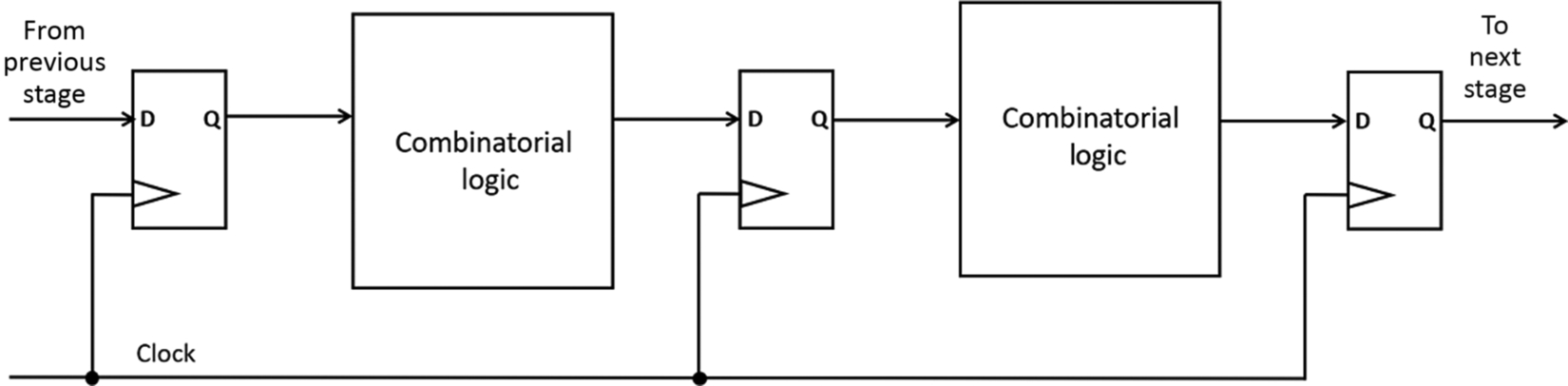
We can illustrate this problem with a simple diagram. Fig. 8.2 shows a simplified schematic diagram of a pipeline, although it could just as easily be a simple finite state machine. The principle is the same. For simplicity, we’ll fold any path length delays into the propagation delays within the combinatorial logic. Suppose that the set-up time for the flip-flop is 500 ps, the propagation delay through the flip-flop is 1 ns, and the slowest combinatorial block in the pipeline has a propagation delay of 4 ns, then the total delay per stage would be 1 + 4 + 0.5 = 5.5 ns. Taking the reciprocal of 5.5 ns, we find that the maximum allowable clock frequency is 182 MHz.
A good example of this discussion [5] is shown in the following Verilog code block:
module timing ( input clk, input [7:0] a, input [7:0] b, output [31:0] c ); reg [7:0] a_d, a_q, b_d, b_q; reg [31:0] c_d, c_q; assign c = c_q; always @(*) begin a_d = a; b_d = b;c_d = (a_q * a_q) * (a_q * a_q) * (b_q * b_q) * (b_q * b_q); end always @(posedge clk) begin a_q <= a_d; b_q <= b_d; c_q <= c_d; end endmodule
When this module is placed into a Xilinx FPGA, the ISE software successfully routed it but failed the timing constraint of a 20 ns maximum data path delay with a calculated delay of 25.2 ns. According to Rajewski, the reason is in the bold line:
c_d = (a_q * a_q) * (a_q * a_q) * (b_q * b_q) * (b_q * b_q);
This line involves many multiplication operations and these multiplications will be instantiated as a complex network of combinatorial logic that is simply too slow to meet the design requirements.
Could we fix this? Perhaps. We might reconfigure this calculation as a pipeline and split the multiplication operation into two steps. This would reduce the propagation delay but could add complexity in other ways.
Because an FPGA is a reprogrammable device, we would assume that the underlying part is inherently stable, assuming that we don’t violate good digital design practices that might lead to metastable states and unpredictable behavior. Contrast this with a custom IC that needs to be validated to a much higher level of rigor.
A good friend of mine related this story to me. He was working for a famous supercomputer company. They made heavy use of FPGAs in their latest design. In order to wring the last bit of performance out of the system, the PC boards containing the FPGAs were hermetically sealed and each FPGA was continuously sprayed with high-pressure Freon to keep it cool. Even with this heavy driving, the FPGA was still being driven within its band of allowable timing specifications. The computer design team noticed that occasionally one of the FPGAs would appear to flip a configuration bit and go off into the weeds.
They consulted with the FPGA manufacturer, who was quite skeptical that any application could cause bit flipping to occur. It was only when they saw the computer in operation and observed the failure did they believe that they had a problem and needed to redesign the part to make it even more tolerant to switching transients. The moral of this story is that even production parts can suffer from glitches under the right conditions.
One interesting aspect of FPGAs that I have not seen much written about is the concept of using the reprogrammability of the hardware environment surrounding the embedded core(s) to build various kinds of hardware-based debug tools. These tools can be looked upon as the hardware equivalent of turn-on or throw-away code to a software engineer. Of course, it is unlikely that once you develop a neat hardware debugger in Verilog, you then toss it. Once you have it and it works, then there is a real-time debugger available anytime. For example, the real complexity inherent in a logic analyzer is tied to the triggering circuitry. The Hewlett-Packard logic analyzers I am familiar with had incredibly flexible (and complicated) trigger circuitry, if you want to use it to track down an elusive bug that didn’t lend itself to a simple break point at an address. This could be done through sequencing, much like a finite state machine circuit.
The HP logic analyzers had seven levels in the sequence. At each level, you could do logic combinations of any number of the bits being used. You could count cycles as well. When a TRUE result occurs, the sequencer could trigger the analyzer to record data or move to the next state in the sequence. A FALSE result could cause the state to remain the same or take you back to a prior state to start again.
But suppose all that you need to do is trigger on an address, data, or status value. It would be relatively simple to build a simple breakpoint comparator in Verilog that would trigger on any combination of bits. The trigger signal could be used to generate a processor interrupt or to trigger a circular trace buffer. The circular buffer is a bit more complicated than a linear buffer, but it has the advantage of being able to capture events leading up to the trigger point as well as what happened after the trigger, or anything in between. Fig. 8.3 illustrates how the circular buffer works.
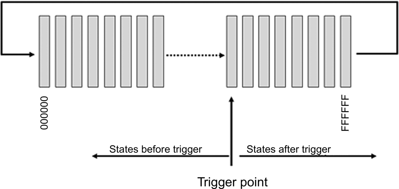
In Fig. 8.3, the buffer holds 224, or roughly 16 million, states. Each memory cell can contain the total number of bits in your logic analyzer. The LA that I am most familiar with could record up to 192 bits wide, although the memory depth was much smaller than 16 M.
In our example, we would have a 24-bit binary counter generating the memory addresses. An address comparator determines where in the buffer we want the trigger point to occur. Thus, the trigger address would be in the range of 000000H to FFFFFFH.
In normal operation, the trace buffer is running continuously and once it records 16 M states, it will start to overwrite previously written data. Another 24-bit countdown counter is also part of the circuit, but is not running until the trigger signal occurs. At that point, it will start to count down from 16 M to 0 and when it reaches 0, it turns off the write signal to the memory buffer, effectively preventing the data from being overwritten. To read out the buffer, reset the memory address counter and read out the data.
Do you need 16 M states and 192 bits in width? Maybe. But likely, you’ll require a subset of the width and a simple buffer to capture the data.
The logic analyzer could be constructed as a peripheral of the embedded core and can be through your debug or validation software. Once you are done with your logic analyzer, some simple additions, perhaps a 64-bit Gray Code counter, can be added to the circuit. Then you can turn the logic analyzer into a real-time performance analyzer.
It gets even better. If you have a spare CPU core in your design, turn that CPU into your logic analyzer controller. Keep it entirely separate from the primary CPU. Here’s an example of the Altera (oops, now Intel) Cyclone V FPGA that I previously mentioned. The text is from the introduction to the FPGA family of parts: [6]
The Cyclone V SoC FPGA HPS consists of a dual-core ARM Cortex-A9 MPCore* processor, a rich set of peripherals, and a multiport memory controller shared with logic in the FPGA, giving you the flexibility of programmable logic and the cost savings of hard intellectual property (IP) due to:
- • Single- or dual-core processor with up to 925 MHz maximum frequency.
- • Hardened embedded peripherals eliminate the need to implement these functions in programmable logic, leaving more FPGA resources for application-specific custom logic and reducing power consumption.
- • Hardened multiport memory controller, shared by the processor and FPGA logic, supports DDR2, DDR3, and LPDDR2 devices with integrated error correction code (ECC) support for high-reliability and safety-critical applications.
If you want to really see what is going on, you can turn the logic analyzer from a state analyzer, where the state acquisition occurs synchronously with the CPU clock, into a timing analyzer by driving it with a separate clock, ideally running faster than the CPU clock. The key idea here is that internal visibility into an SoC based upon the FPGA architecture is possible to achieve.
I’ve often had discussions with my colleagues regarding my insistence on making real measurements versus simulations. This usually centers around my focus on teaching how to use a logic analyzer in my microprocessor class. Someone will point to the data sheet for some FPGA simulation tool and show me the built-in logic analyzer that runs within the simulation. So, why bother with measuring real circuitry, just run simulations?
I have to admit that they have a point. Simulations are getting better and better, particularly the FPGA design tools, and the ones we use are free for the downloading! What a deal. But…. logic analysis, as a debug methodology, is so fundamental to what a hardware engineer needs in her toolkit that I just can’t imagine relegating it to the pile of obsolete electronics that you find in the surplus stores.f
Lauterbach GMBH offers one of the most extensive set of development and debug tools specifically designed for debugging embedded cores. Their TRACE32 debug tool family supports an impressive range of hard and soft embedded cores for both trace and debug. The trace buffer can be configured on-chip or through a parallel port to a trace buffer on the host computer, which provides an almost insanely large trace buffer of 1 T frames. Fig. 8.4 is a schematic diagram of the Lauterbach system.

As you can see, multiple cores can be connected to on-chip trace generation logic, as I’ve described, then to the trace buffer. This information can then be downloaded through the JTAG port to the TRACE32 user interface to be analyzed in the same way that you would analyze a board-level embedded system. The flexibility of the FPGA enables logic analysis modules to be added for critical debugging stages and removed if the space is needed for additional functionality. Intel, Lattice, and Xilinx offer configurable modules for integration into their FPGA families. Intel offers the Signal Tap Logic analyzer. Lattice offers Reveal and Xilinx offers the ChipScope analysis blocks.
Because you can expect to pay for the commercial LA blocks, I was curious to see if there were any public domain logic analyzers that I could recommend. I found one such homebrew on a blog [7] and the authors reference some other work. However, be forewarned. Playing with open source software may be a bigger time suck than just purchasing a license to use the commercially available modules.
Gisselquist [8] describes in a rather complete set of instructions how he built a 16-bit in-circuit logic analyzer in Verilog. He goes step by step through the subblocks and then provides an example application.
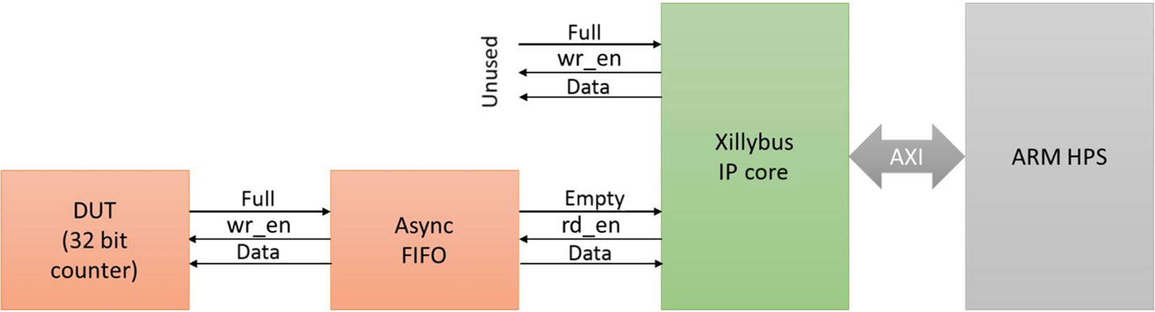
Another excellent example [9] was a final project of Mohammed Dohadwala, a student in ECE 5760, Advanced Microcontroller Design, at the Electrical Engineering School of Cornell University.g This system was implemented on a Terasic DE-1 FPGA Boardh that was based on the Intel (Altera) Cyclone V FPGA, which contains an ARM dual-core Cortex A9 hard core. The full report is available online (see reference). What I like about his design is that it uses a 32-bit wide, 512 element deep FIFO (memory), rather than a standard trace buffer. This enables him to run the logic analyzer at 100 MHz while still being able to stream the data to an external data logger. A key element of the design is an IP block called XILLYBUS,i which provides a DMA function over PCIe I/O protocols. The bus is designed to work with Xilinx Zynq-7000 EPP and Intel Cyclone V SoC.
This logic analyzer is designed to be controlled by the onboard ARM core and runs under Linux. As such, its primary use would be to debug the other functional blocks in the system rather than the CPU core. Fig. 8.5 is a block diagram of the system.
Virtualization
Today, we have PCs that have performance numbers that the workstations of 10 years ago could only dream about. With that computing power, multiple gigabytes of RAM, and fast solid-state drives, it is possible (with the appropriate software) to completely model a system, whether it is an SoC or a board-level system with discrete components.
Virtualization is not a new technology, per se. Instruction set simulators have been around for a long time. Apple iMac computers can run Windows software in a virtual PC. The key to the major advancement in the technology is the idea of a hypervisor layer that sits beneath the processor and its supporting hardware. This hardware includes memory, so in a multicore environment or a multiprocessing environment, each core or virtual processor can run independently of the others. This is convenient if, for example, you wish to run different operating systems on each core. Another virtue is that it provides a level of security that prevents a hacker who may gain access to one virtual machine to then get a jumping off point to other virtual machines running high-security applications.
In a Technology White Paper, Heiser [10] describes how his OKL4 kernelj hypervisor can protect a communications stack in a cell phone from a virus-infected application. He goes on to point out that even with multiple cores, there is a danger if the cores share a common memory bank.
Another name for the hypervisor is the virtual-machine monitor, or VMM. According to Popek [11] and cited by Heiser, the VMM must have three key characteristics:
- 1. The VMM provides to software an environment that is essentially identical with the original machine.
- 2. Programs run in this environment show, at worst, minor decreases in speed.
- 3. The VMM is in complete control of system resources.
Condition 1 guarantees that the software designed to run on the bare hardware (actual machine) will also run (unchanged) on the virtual machine. Condition 2 is important because if the virtualization is to be able to run in real time, it must not suffer a performance hit so bad as to prevent time-critical code from executing properly. The third condition must guarantee that there is no back door around the VMM and that one application is completely isolated from any other.
In the OKL4 kernel running with an ARM core, the memory management unit (MMU) on the ARM core is used to provide a hardware-based isolation mechanism. The author draws a distinction between the VMM as defined by the hypervisor as a system-level virtual machine in order to distinguish it from a process-level VM, such as the JAVA virtual machine.
In embedded systems, the hypervisor enables multiple operating systems to exist concurrently. Why is this an advantage? The cell phone, for example, contains devices with real-time requirements and applications that resemble those on your PC. Thus, an RTOS can be used for the time-sensitive applications and a traditional O/S, such as Linux, can be used to control the time-insensitive applications.
So far, we’ve discussed virtualization as a strategy for use on a system in operation, not under development. However, it doesn’t take a great leap to see that this can also be used as a powerful design environment as well. Wind River Systemsk offers Simics, a virtual design environment that enables complete system simulation. As stated in Wind River’s product overview document [12]:
Software developers use Simics to simulate nearly anything, from a single chip all the way up to complete systems and networks of any size or complexity. A Simics simulation of a target system can run unmodified target software (the same boot loader, BIOS, firmware, operating system, board support package (BSP), middleware, and applications as the hardware), which means users can reap the benefits of using a pure software tool.
Fig. 8.6 shows a schematic diagram of the Simics system.
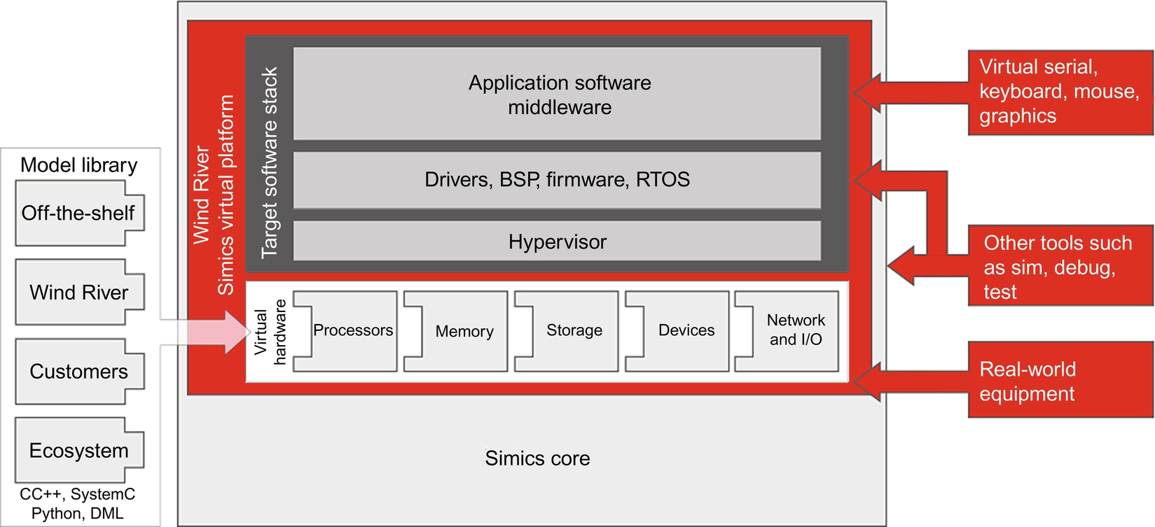
The Simics environment enables a complete system simulation that enables the software team to develop and debug their code in a continuous manner, rather than waiting until target hardware is available at the start of the HW/SW integration phase. According to the product overview document, the value of Simics for the integration and test phase of a product development life cycle may be summarized as follows (their bullet points):
- • Start testing and automation early in the development process. Do continuous hardware and software integration early, on virtual hardware, expanding to physical hardware as it becomes available.
- • Build more levels of intermediate setups than are available with hardware, to facilitate continuous integration.
- • Test fault tolerance with Simics fault injection. Cover corner cases that cannot be reached in hardware.
- • Automate and parallelize testing and expand coverage of target configurations using Simics scripting.
- • Save developer time, reduce waiting time to run tests, and shorten feedback loops by using simulation labs in addition to hardware labs.
- • Do test and integration on the entire system by integrating Simics models of computer hardware with external models of the physical world or system environment.
- • Automate regression testing and continuous integration by tying Simics into existing workflows of software build and test.
Of particular interest to me in the context of this book is the assertion regarding debugging:
Complex and connected systems are difficult to debug and manage. While traditional development tools can help you track down bugs related to a single board or software process, finding a bug in a system of many boards and processor cores is a daunting task. For example, if you stop one process or thread with a traditional debugger, other parts in the system will continue to execute, making it impossible to get a globally coherent view of the target system state.
Simics provides access to, visibility into, and control over all boards and processor cores in the system. Single-stepping forward and in reverse applies to the system as a whole; the whole system can be inspected and debugged as a unit. Furthermore, a checkpoint—or snapshot—can be created, capturing the entire system state. This state can be passed to another developer, who can then inspect the precise hardware and software state, replay recorded executions, and continue execution as if it never stopped.
Of course, the devil is in the details. I have not investigated the investment required in acquisition costs, licenses, training, and deployment to know if this is a good investment for any particular application, such as yours. My interest is only to help make you aware of the tools that are currently out there waiting for you. My best advice is to contact the vendors I’ve referenced and invite them in for a demonstration.
Another great way to see these products in action is to attend the next Embedded Systems Conference.l It is pretty easy to score free tickets to the exhibition floor, though it will generally cost you to attend the technical sessions. Speaking of the technical sessions, I am the proud owner of several Embedded System Conference Speaker polo shirts, which I proudly wear as my fashion statement.
If you can’t, or don’t, wish to attend the technical sessions, you can usually purchase a DVD of the proceedings. However, the real objective of the conference is the exhibition floor. There you can see Simics or other tools in operation and speak with engineers who are incredibly knowledgeable about the product. If you are really fortunate, you can meet with one of the R&D engineers who actually designed it, and because they do not have the brain filter of marketing and sales folks, you’ll get the straight skinny, engineer to engineer, until the marketeer comes by and shoos them away (just kidding).
Conclusion
In this chapter, we’ve examined the tools that are relevant to trying to debug embedded cores. The issue is how do you look inside the FPGA to find and fix the bugs? Fortunately, the FPGA is an incredibly flexible device that, in my opinion, will revolutionize computing as we know it.
As an aside, during this past year, there was a lot of press coverage of the technology issues surrounding the security aspects of the Huawei data switch. While I don’t know enough to know if these are real concerns, I noted in one of the technical discussions that the data switch used FPGAs as part of the machine’s architecture. Thus, while it would be possible for people worried about the security of the switch to examine the CPU code, it is entirely possible for a bad actor to reprogram the FPGAs to sniff the data going through the switch. Just a thought.
The tools that we’ve discussed here provide the internal visibility that is needed. Once the visibility is achieved, the same debug techniques that were discussed in earlier chapters come into play. For example, keep a record of your observations, hypotheses, tests, and results. Change only one thing at a time and log any differences you might observe.
Another observation I could make is that from my examination of the tools, or at least the printed literature, I get the impression that there is likely a significant learning curve associated with becoming proficient and comfortable with them. This will require a time investment and up-front planning to allow time in your schedule for training. It can be really frustrating (I know, I’ve been there) to know exactly what you want to test, or do, but you can’t decipher how to do it, and the documentation is of little or no help.
Onward.
Additional resources
- 1. https://www.eetimes.com/author.asp?section_id=36&doc_id=1284571#.
- 2. https://www.electronicproducts.com/Digital_ICs/Standard_and_Programmable_Logic/Debugging_hybrid_FPGA_logic_processor_designs.aspx.
- 3. https://www.embedded.com/design/other/4218187/Software-Debug-Options-on-ASIC-Cores.
- 4. https://www.edn.com/design/systems-design/4312670/Debugging-FPGA-designs-may-be-harder-than-you-expect.
- 5. https://www.newark.com/pdfs/techarticles/tektronix/XylinxAndAlteraFPGA_AppNote_MSO4000.pdf.
- 6. https://www.xilinx.com/video/hardware/logic-debug-in-vivado.html.
- 7. https://www.dinigroup.com/files/DINI_DR_WhitePaper_031115.pdf.