
12: Memory systems
Keywords
Soft errors; Jitter; Eye diagram; Cosmic rays; FIT; Alpha particles
Introduction
You could say that we’ve saved the best for last. Memory is the heart of your system. As with most aspects of embedded systems, memory debugging has a hardware and a software component. Before we can debug software issues, we need to make certain that the hardware is both functional and reliable. Therefore, I would argue that the first testing and possible debugging that should be done must be the processor-to-memory interface.
If the memory is internal to your microcontroller, there isn’t much debugging to do outside making certain that all the configuration registers are properly initialized. If the microcontroller is also addressing external memory, then the same issues arise as with any external processor/memory interface.
In this chapter, we’ll first explore the basics of memory debugging using static RAM (SRAM) as our model and then move on to a general discussion of DRAMs and DRAM debugging methods. Discussing the nature of how RAM works is crucial to having insights into the possible root causes of an error or defect.
After discussing hardware-based error-chasing techniques, we’ll look at memory bugs that are software-based.
General testing strategies
In a very thorough article on testing RAM in embedded systems, Ganssle [1] discusses general strategies for testing RAM memories in embedded systems. His first observation is that the RAM test should have a purpose. He says,
So, my first belief about diagnostics in general, and RAM tests in particular, is to clearly define your goals. Why run the test? What will the result be? Who will be the unlucky recipient of the bad news in the event an error is found, and what do you expect that person to do?
If you suspect a hard RAM failure, it may manifest itself in several ways. If you’re lucky, the system will detect it, report it, and try to recover. If not, the system will crash. If this is an intermittent problem, you may not learn about it until customers start to complain, or there’s a catastrophic failure and people are injured.
Ganssle goes on to debunk my favorite memory test pattern, alternating 0xAA and 0x55 bit patterns, and provides good reasons why these patterns are rather poor for any kind of extensive and thorough memory test. One reason that the alternating 0xAA/0x55 test is so poor is that if the problem has to do with memory addressing, there is a 50% probability that writing and reading back from the wrong address will still pass as good memory.
He suggests constructing long strings of almost random bit patterns and testing with them. If the string happens to be a prime number (Ganssle suggests 257), then repeatedly writing and reading to blocks of memory will not map in multiples of memory blocks with the same address bits, differing only in the higher order bits.
Another good tip from his article is to write an entire block first, then read it back and compare. Testing small blocks at a time will not find all errors.
Poor memory design will often manifest itself as sensitive to a particular bit pattern while working perfectly with most other random reads and writes. While we might attribute this to a bad chip, the likelihood, as Ganssle points out, is more likely to be bad PC board design practices, such as inadequate power bus filtering, electrical noise, inadequate drive capabilities, or one that can sneak up on a digital designer, the dreaded “analog effects.”
Most digital designers, including me, would almost never think about terminating address, data, and status buses between the processor and the external memory. A good design guideline [2, 3] gives a general rule of thumb for deciding when you need to properly terminate a trace in its characteristic impedance.
The speed of a signal on a printed circuit board is approximately 6–8 in./ns, about half the speed of light in free space. Assuming the value of 6 in./ns, then you should terminate the trace if the trace length is greater than 3 in./ns of rise time of the trace. So, a pulse with a rise time of 1 ns can be left unterminated if it is less than 3″ in length. Of course, as edges get even faster, this value will decrease even more. This is pretty sobering if you are working with gallium-arsenide (GaAs) logic with rise times around 100 ps. There, any trace over approximately 5/16 to 3/8 of an inch needs to be terminated. Fortunately for most of us, that’s a different world.
When and if to choose to use line driver circuits can be a tough decision. You’ll incur power, access time, board area, and cost penalties if you use drivers. However, memory arrays, or particularly DRAM arrays, as Ganssle points out present a large capacitive load to the output pins of the processor writing to memory. Most microdevice outputs are not designed to drive capacitive loads. As a result, rise times may become unacceptably slow, leading to noise and instability problems.
Static RAM
Whether you are using a microcontroller with onboard RAM or a microprocessor with external RAM, the workings of the system in both cases are the same. As its name implies, this RAM is static. As long as power is applied, the data stored within its cells are stable. Writing to the RAM cell can change the data and reading from the RAM cell leaves the data unchanged.
Static RAM can be very fast and is always accessible. On the other hand, dynamic RAM contains overhead that will sometimes prevent immediate access to it. Why then isn’t static RAM the dominant memory architecture in modern computers? The simple answer is density. Dynamic RAM requires one transistor to store one bit of data. A static RAM cell typically requires four or six transistors to store one bit of data.a
Fig. 12.1 is a schematic representation of a typical static RAM cell consisting of two inverters, A and B, and two switches, C and D. Each inverter contains a CMOS pair and each switch is a single NMOS transistor, thus yielding a six-transistor memory cell.

Referring to Fig. 12.1. Assuming that the value at switch D represents the data stored in the cell, if switch C is momentarily connected to ground, the output will flip from a 0 to a 1 and switch C can be opened without changing the data stored in the cell.
SRAMs excel in any application that requires completely random access to any address in memory with no latency. DRAM, though much denser, is superior in applications where sequential access is the most common because the DRAM architecture is optimized for operating with on-chip caches in the CPU. As a simple figure of merit, the largest SRAMs are of the order of 16–18 megabits (Mbits) while DRAMs can be found up to 16 gigabits (Gbits). More on this later.
SRAMs come in two main varieties, synchronous and asynchronous. Asynchronous is the easier to understand, so we’ll consider that one first. Fig. 12.2 is a greatly simplified schematic diagram of a typical 32 Kb (256 Kbit) SRAM.

The SRAM has 15 address inputs, labeled A0–A14, and 8 inputs and outputs that would be connected to the processor’s data bus.
There are three control inputs, all active low. These are:
- • Chip enable ¯CE
 : Master chip controller. Must be asserted for any read or write operation.
 - • Write enable ¯WE
 : Must be asserted when data is to be written into the device.
 - • Output enable¯OE:
 Must be asserted when reading the contents of the memory is required.
Note that ¯WE![]() and ¯OE
and ¯OE![]() are mutually exclusive. You should not assert them both at the same time.
are mutually exclusive. You should not assert them both at the same time.
The operation of the asynchronous SRAM circuit is quite straightforward. Let’s consider a READ operation. The 14 address bits are applied to the device and must be stable for some period of time before the chip enable or output enable input are asserted. With the address bits and control inputs stable, data will appear of the 8 I/O pins and may be read by the processor after the appropriate time delay, called the access time, occurs. Fast SRAMs have access times of 15 ns or faster while slow SRAMs might have access times 40 ns or higher. Anything between the two is up to the marketing department.
On the other side of the wall, we have the processor. It has its own set of timing specifications dictated by its clock and finite state machine that controls bus operation. Suppose our memory has a 50 MHz clock and every memory cycle requires 4 clock cycles. For simplicity, we’ll further subdivide these 4 clock cycles into 8 half clock cycles and label them φ1 through φ8, representing eight phases of the state machine.
Referring to Fig. 12.3, a memory cycle starts with a new memory cycle starting in φ1. Addresses begin to change and are stable around the beginning of φ3. This is indicated by the assertion of the address valid (ADDR valid) signal about midway through φ3. At the same time, the read (¯RD)![]() signal becomes active and, as they say at NASA, “The clock has started.”
signal becomes active and, as they say at NASA, “The clock has started.”

We can see from the diagram that the READ signal starts halfway through φ3 and ends halfway through φ8. Therefore, we have a total of 5 half clock cycles. Because we have a 50 MHz clock, each full clock cycle is 20 ns. Thus, we have 5 half clock cycles and each half clock cycle is 10 ns, giving a total time duration of 50 ns from the time that the processor asserts that a memory READ operation is taking place to the time that it actually reads in the data from memory on the rising edge of the ¯RD![]() signal.
signal.
Any static RAM memory faster than 50 ns will work in this application. Any memory with a rated access time of 50 ns or slower may work in this application, but the manufacturer will not guarantee it under all operating conditions.
What I haven’t shown on this simplified timing diagram is how the processor deals with memory that may have access times longer than 50 ns. We could slow down the processor’s clock, but that slows everything down. The best solution if we can’t get faster memory devices is to extend the time duration from the assertion of READ to the deassertion of READ. There are various hardware methods to do this, but they all fall under the general umbrella called “wait states.” For example, a wait state in this system could simply extend the φ5 and φ6 phases one full clock cycle, giving us φ5, φ6, φ5′, and φ6′. Adding this wait state changes the maximum access time requirement from 50 to 70 ns. Adding more wait states just continues the process until the memory access time meets our specification.
Some processors have programmable wait state registers that can be used for specific memory regions. ROM memory is typically slower than RAM memory, so if you are seeing intermittent failures, one debugging strategy would be to add a wait state and see if that improves it.
As an example, the NXP ColdFire microcontroller family was a very popular successor to the original Motorola 68 K family. It was “mostly” code compatible, with some 68 K instructions no longer supported. Of note for this discussion are the eight internal chip-select registers that allowed the user to program:
- • Port size (8-, 16- or 32-bit).
- • Number of internal wait states (0–15).
- • Enable assertion of internal transfer acknowledge.
- • Enable assertion of transfer acknowledge for external master transfers.
- • Enable burst transfers.
- • Programmable address set-up times and address hold times.
- • Enable read and/or write transfers.
The chip-select registers could each be independently programmed for the type of memory and its access characteristics occupying up to eight different regions of memory.
I have some familiarity with this processor because I used it when I taught an embedded systems class for computer science students, rather than electrical engineering students. In their lab class, they had to learn to wade through the dense sea of acronyms in the user’s manual to try to figure out how to correctly program the registers with their set-up code before the processor is ready to accept application code.
In the context of debugging, properly programming the many internal registers of a modern microcontroller is not a task for the weak of heart. Microcontrollers should come out of RESET in an operational limp-mode. This enables the programmer to be able to set up the operational registers in order to establish the runtime environment. Making sure that these registers are correctly set would be the first step in any memory debugging plan.
Here’s one scenario. Everything seems to be working but the system seems to be running slower than it should be. Rechecking the chip-select registers shows that you’ve programmed four additional wait states by placing a 1 bit in the wrong field of the register.
When we have a microcontroller with internal chip-select registers, then the timing diagrams for external memory accesses will be correct as presented because the chip manufacturer has already accounted for the time to generate the chip-select signals in the timing specifications. However, if you are designing the external memory system and you are also designing the decoding logic, then you must also allow for the decoding logic for the external memory.
Here’s a simple example. Let’s assume that you have an 8-bit processor accessing external memory. The external memory is comprised of four static RAMs. Each SRAM is organized as 1 Meg deep by 8 bits wide. Your processor is capable of addressing 16 Meg of external memory, requiring 24 external address lines. Each SRAM chip requires 20 address lines, or A0–A19, 2 more address lines are used to select 1 of the 4 SRAM devices, A20 and A21, and 2 address lines, A22 and A23, are not needed.
You could leave A22 and A23 unconnected but then you might have to deal with the SRAM appearing 4 times in the processor’s external memory space because the decoding logic won’t decode those 2 address bits. I would include them in my logical equations, but that is your call.
There are many different ways to implement the decoder, and my intent is not to go through a design exercise. Let’s just say you decide to implement the decoder in a programmable logic device, or PLD, with a worst-case propagation delay time of 15 ns over all conditions.
Referring back to Fig. 12.3, then the 50 ns that we had now becomes 35 ns because we’ve just lost 15 ns decoding the upper address bits and then enabling the proper chip-enable pin on the SRAM. Thus, we either must use faster SRAMs or add an additional wait state.
Here’s where it gets tricky. It might work as is for the prototype circuit that the designer has been working on. If your company also does environmental testing, it may or may not continue to work at temperatures closer to 70°C. If you are really lucky, you have a fast batch of 50 ns SRAMs and it even works at temperature. Then, you go to production and the systems start failing in the field because the production lots you are buying are slower than your prototype batch.
At this point, we can get into a very deep discussion about hardware design strategies and using worst-case numbers rather than typical timing values in a design. Is it a design flaw or a bug if some systems fail while others keep working? Would using worst-case numbers compromise the performance of the system or the desired price point? These are not easy questions to answer. However, trying to find the reason for an intermittent failure is tough and possibly very time consuming. Because the memory system is at the very core of any computer system, the debugging process must start with a full timing analysis, followed by measurements with an oscilloscope or logic analyzer capable of time-interval measurements that are better than what you think you need. In this example, a 100 MHz oscilloscope might not be sufficient, but is likely at the edge of being able to show you the relative timing relationships.
A logic analyzer with 2 ns timing resolution would certainly show the timing relationships, but will not show you any analog effects such as slow edges, ringing, or bus contention problems. You need both instruments to do a really thorough job.
I would also consider doing a differential measurement and compare a unit that is intermittently failing with one that is rock solid and compare signals. Record your measurements, capture screen images, and compare waveforms. If you can, do another differential experiment. Replace the SRAMs on your prototype board with the SRAMs from the production batch and rerun your tests. Compare the waveforms with the previous ones. It is always possible to have a bad batch or a good batch that is markedly different than an earlier one.
The last test I would perform is an extensive memory test at room temperature and over a wider temperature range. The memory test should cover the basics test patterns, 00, FFH, AAH, 55H, walking ones, and walking zeros.b Any memory failure should stop the test with some indication of where it failed and what pattern was written and what pattern was returned.
Because this is a differential measurement, you want to change just one, and only one, variable at a time. If you are testing the failing board inside a device, and you are testing your reference board using your bench supply, then the first differential measurement would be to swap the device’s power supply with your bench supply. Because most products don’t ship with $500 lab power supplies, perhaps that’s worth investigating.
If you don’t have an environmental chamber at your disposal, then find a multimeter with a thermocouple input and tape the tip of the thermocouple down to one of the SRAMs. Try to close up the chassis to make the test as real as possible. Is the SRAM getting hotter than you would expect? Is the ambient temperature inside the chassis hotter than you anticipated? Repeat the test with your reference board in the chassis and compare results.
All the while, use the best practices that were discussed in previous chapters:
- • Write down what test you are going to do and what you hope to find out.
- • Record your results.
- • Analyze your results and use the analysis to guide the choice of the next test to perform.
As I write this chapter, I’ve been struggling with a problem with a design I did for a student lab experiment to teach how to use logic analyzers. I would have never even thought to mention this as a potential problem before now. The board uses a PLD to do address decoding and generate wait states for the students to observe how they affect performance.
I bought the PLDs from a reputable vendor who has been a reliable supplier for many years. The first batch of 20 parts were from a different manufacturer, but my programmer could program that part from that manufacturer in the package style I was using. I thought, “No problem,” until I tried to program them. Not one would program correctly. I tried a second programmer that the students use. Same result.
I ordered a second batch and this time I specified the manufacturer. I received 10 parts. Nine programmed properly and one failed to program. I contacted my supplier and they sent me a replacement. The replacement also failed to program, but this time the error was a mismatch in the electronic ID that the programmer reads from the PLD to make sure the correct part is being programmed. We ordered another 20 parts, and I’ll see what happens. My suspicion is that my supplier received a batch of defective or bogus parts.
Why do I mention this? Counterfeiting of integrating circuits has become a very profitable criminal activity in recent years because it is so easy to relabel a part and charge a premium price for it. Perhaps you purchase an SRAM with a 15 ns access time and what you receive are parts with 25 ns access times. If your company purchases parts through distribution rather than directly from the manufacturer, now you have to debug the supply chain.
My point here is that debugging a hardware issue may encompass a much wider set of circumstances than you initially thought. Ideally, you’ll zero in on a set of test conditions that causes the memory system to consistently fail. Then you are almost home. There is a light at the end of the tunnel.
Dynamic RAM
Unlike SRAM, dynamic RAM, or DRAM, gets its name from the fact that it cannot be left alone and be expected to retain the data written into it. When we examined the SRAM cell, we saw how the positive feedback between the gates making up one bit of storage forced the data bit into a stable state unless some external action (data being written) was taken to flip it.
A DRAM cell has no feedback to maintain the data. Data is stored as charge trapped in a capacitor that is part of the bit cell. At temperatures well above absolute zero, such as the commercial temperature range of 0–70°C, the stored charge has thermal energy and can leak away from the capacitor over time. The mechanism to restore the charge is through a refresh cycle. Refresh cycles are a special form of access that appears to be a data read, but the only purpose is to force the DRAM circuitry to restore the charge on a bank of capacitors at the same time. Typically, every bank in the DRAM array must be refreshed ever few milliseconds.
The refresh operation is accomplished by interleaving the refresh cycle with regular memory accesses. Some refresh cycles can be synchronized with the processor clock and are built into the regular bus cycle. The trusty old Z80 CPU had a refresh cycle woven into its regular bus cycles, so memory access never suffered if memory needed refreshing when the processor was trying to access it. When processors don’t have built-in refresh capabilities, external hardware such as refresh controllers must be included in your design to handle refreshing and bus contention between the refresh housekeeping requirements and memory access. On PCs, this function was taken over by the Northbridge. This chip connects the CPU to the memory system and provides the proper timing interface to manage the system with a minimum of bottlenecks.
Another major departure in the design of DRAM versus SRAM is how memory is addressed. This comes about because of the relative capacity of DRAM chips and SRAM chips. Today, the leading edge in DRAM technology is 32 Gbits. For SRAM technology, the leading edge is 32 Mbits. That’s a factor of 1000 in memory density. This is important because, depending on the organization of the chip, whether it is by 8, by 16, or by 32, all those memory locations require address lines between the processor and memory.
In order to reduce the number of address lines, DRAM chips have evolved a number of strategies. The first technique that DRAMs developed was to split the address into two parts, a row address and a column address. These names are associated with the internal memory array of DRAM cells. If you picture a two-dimensional matrix of DRAM cells, each row of the matrix can be uniquely identified by an address and each column of the matrix can be uniquely identified. The intersection of the row number and the column number uniquely identifies each cell in the matrix of data bits. To create a 16 Gbit DRAM that was organized as 2G by 8 bits, you would need to have eight matrices, each one holding 2 Gbits of data. Each of the 8 matrices would be organized as a 216 by 215 array, or 64 K by 32 K. Depending on how the rows and columns are organized, we could have a 16-bit row address and a 15-bit column address.
A simple DRAM memory access requires that the row address be presented to the DRAM, and Row Address Strobe (¯RAS![]() ) input is asserted to lock in the row address. Next, the column address is presented to the DRAM and the column address strobe (¯CAS
) input is asserted to lock in the row address. Next, the column address is presented to the DRAM and the column address strobe (¯CAS![]() ) is asserted. This completes the addressing operation and data can now be written or read.
) is asserted. This completes the addressing operation and data can now be written or read.
Fig. 12.4 is a timing diagram for a simple DRAM read cycle [4].

All the I/O signals are the same as for the SRAM, with the exception of the RAS and CAS strobe inputs to the DRAM. It should be obvious that there are complex timing relationships between these signals and designing a DRAM controller is not for the faint of heart. Fortunately, microcontrollers and external support chips have greatly simplified the interfacing to DRAM, but the possibility always exists for erroneously programming the internal registers of the DRAM controllers. Here’s where a fast oscilloscope can be a very valuable tool to use to examine signal timing and signal integrity of DRAMs.
It may seem that DRAM should be slower than SRAM because of the added overhead of refreshing and the need for RAS and CAS. Actually, for many operations, the DRAM can be faster than the SRAM. While the first DRAM access might be slower, subsequent accesses are incredibly fast because modern DRAM technology has evolved hand in glove with modern CPU architectures, in particular, on-chip program and data caches.
The normal DRAM operating mode is to set up the first address of an access and then issue successive clock pulses that bring in subsequent sequential data on every phase of the clock. We call this double data rate or DDR DRAM. This DRAM is synchronous with a clock, which may be the internal clock of the processor or a derivative of that clock. This “burst” access is designed to be very compatible with the design of the on-chip caches.
The operation goes something like this. The processor attempts to access a memory location and the cache-controller looks for that address within the address or data cache. If it determines that it is not in the cache, then the address goes out to external memory. After a number of clock cycles to set up the memory transfer to the cache, the data moves from the DRAM memory on alternate phases of the clock until one row of the cache, perhaps 32 or 64 bytes, is filled. Notice how the size of the burst matches the size of the cache storage region. The burst transfer will occur even if the processor only needs a single byte of data from memory.
While this creates a really tight bonding between the memory and the processor, there is a dark side to this architecture. Suddenly, a new dimension has been added to the ways in which a program could, for no apparent reason, start to run very slowly, perhaps by a factor of 10 or greater, yet the hardware is functioning perfectly well.
Depending upon the nature of the algorithm you are running, the performance of the cache may vary dramatically. This is called the “cache hit ratio,” which is defined as the ratio of the number of accesses to a cache and the number of accesses where the cache held the instruction or data the program was looking for. So, if the required data was already in the cache 9 times out of 10, then the cache hit ratio is 90%.
But suppose we craft an algorithm in such a way that the processor is executing repetitive code in a way that each time, part of the data loop is never in the cache and must be fetched from memory. We already saw that the burst is fast but setting up the burst is slow. If the processor is continually requiring cache fills, then the overall performance will fall off a cliff. This is generally called thrashing and refers to the constant need to fill and then refill the cache.
To add to the complexity, we also have to account for the effect of the CPU execution pipeline. Modern processors have deep pipelines because instructions can be complex, and the time required to decode and execute the instruction is greater than the 250 ps long clock period of a 4 GHz system clock. Some modern pipelines are more than 20 stages long. While this is not a problem as long as the instructions are all in a long line, a loop will cause the pipeline to be flushed and refilled. Now we have three interacting systems, the DRAM, the cache, and the pipeline.
Unfortunately, I can’t give you a simple process to debug poor performance. However, a lot of engineer-centuries have gone into optimizing this system at the PC level. It involves close cooperation between the processor companies, the DRAM manufacturers, the support chip manufacturers, and the compiler designers with a common goal of optimizing the overall performance of the system.
The takeaway here is that if you are using DRAM in an embedded system, unless you are just using a PC as an embedded controller, then these are issues that you may well have to deal with. We discussed the EEMBC benchmark consortium in Chapter 6 on processor performance issues. These realistic industry-specific benchmarks provide a baseline for looking for performance issues with your system.
Soft errors
As engineers, we are comfortable fixing problems that are reasonably deterministic, even if the circumstances that cause the problem are extremely rare and very infrequent. But what if the problem occurs for reasons that we can only guess at and generally attribute to, “it came from outer space?” Imagine telling that to your manager. That’s right up there with, “The dog ate my homework.”
But it is true. The first source of soft errors was traced to cosmic rays from space. These energetic particles are constantly bombarding us many thousands of times per second. Most just pass right through us and most of the planet, and keep on going. Every once in a while, a cosmic ray will interact with matter. In the case of a DRAM, this is the capacitor that is holding the charge for the bit cell. If the energetic particle hits just right, it can produce a shower of electrons that can change the value of the bit stored in the cell. That is a soft error.
Texas Instruments [5] also cites alpha particles emitted from impurities in the silicon as a source of soft errors, along with the cosmic background neutron flux that is present at low radiation rates at sea level and much higher rates at the flight altitude of aircraft. They also note that alpha radiation can be minimized by the use of ultralow alpha (ULA) materials, but because it is very difficult to shield materials from neutrons, a certain level of soft errors is inevitable.
A white paper by Tezzaron Semiconductor Company [6] concluded that in a 1 Gbyte DRAM memory system, there is a high probability that you can expect a soft error every few weeks, and for a 1 Tbyte memory system, that reduces to one soft error every few minutes. Fortunately, we typically find 1 Tbyte memories in big server systems that would use memory that includes extra bits per byte for on-the-fly error correction. Quoting Tezzaron’s conclusion,
Soft errors are a matter of increasing concern as memories get larger and memory technologies get smaller. Even using a relatively conservative error rate (500 FIT/Mbit), a system with 1 GByte of RAM can expect an error every two weeks; a hypothetical Terabyte system would experience a soft error every few minutes. Existing ECC technologies can greatly reduce the error rate, but they may have unacceptable tradeoffs in power, speed, price, or size.
Way back in the early days of the PC when DRAM “sticks” first hit the mainstream, most DRAM modules contained nine DRAM chips rather than eight. The extra bit was a parity bit. Assuming that you’ve set up your BIOS to check for ODD parity, the hardware will count the number of 1 bits in each byte written to memory and if the number of 1 bits is an even number, the parity bit is set to 1. If the number of bits in the byte is an odd number, then the parity bit is set to 0. When the system reads a memory location, it computes the parity of each byte read back on the fly. If the parity computes to EVEN, then a memory error occurred.
I can remember my PC suddenly freezing with a “memory error” message, but I couldn’t tell if it was due to a cosmic ray, a random error, or my PC acting up. So, I rebooted and moved on. If I lost the work I was doing, I muttered some expletives and resolved to save my work more often.
Debugging these errors is nearly impossible unless it happens often enough to devise a debugging test. Perhaps running extensive memory tests for hours or days and not finding an error would at least give you confidence that the hardware is stable and reliable.
The Tezzaron analysis goes on to say that DRAM today is less susceptible to cosmic ray-induced soft errors because while the transistor bit cell has been shrinking, the size of the stored charge needed has not been dropping at the same rate, so the noise margin for error has improved. However, cosmic rays can still play havoc with dense memory systems.
Recent work [7] compared the soft error rate in 40 nm commercial SRAMs by measuring the error rate on a mountaintop and at sea level over the course of several years. The results correlated with the measured neutron flux at both locations. While the root cause mechanisms for SRAMs and DRAMs may be different, studies assert that with today’s finer geometries in both SRAMs and DRAMs, soft error rates are roughly comparable. RAM-based FPGAs may also be susceptible to bit flipping and, as one could imagine, the results can be disastrous if the hardware suddenly goes belly-up.
As I discussed in a previous chapter, but is relevant here as well, was the experience of a former colleague who went to work for a supercomputer company. He told me about this experience they had with a new system under development that made heavy use of FPGAs. The FPGAs were mounted on a hermetically sealed printed circuit board and each FPGA sat under a nozzle where a high-pressure stream of Freon refrigerant was pumped onto it to cool it.
The engineers noticed that the electrical noise levels generated in these parts due to the way that the parts were being driven were sufficiently high to flip bits in the configuration memory of the FPGA, even though the parts were being used within their vendor’s parametric limits. It wasn’t until the FPGA vendor’s engineers came out and saw it for themselves did the company realize that they had a design issue with their parts.
SRAM manufacturers are aware of the issue and are directly addressing the problem in their current product offerings. Cypress Semiconductor Corp. expressly discusses the addition of on-chip error code correction (ECC) below 0.1 FIT/Mbit [8].c With the addition of on-chip soft error correction, Cypress claims a soft error rate below 0.1 FIT.
In addition to on-chip error correction, semiconductor manufacturers are utilizing a new CMOS geometry called FinFET [9]. FinFET is a three-dimensional structure, as opposed to the traditional planar geometry of the MOS transistor. With FinFET, the gate and the gate oxide are wrapped around the fin-shaped source to drain channel.
Villanueva [10] calculated the soft-error rates for a 6-transistor (6 T) FinFET SRAM cell using 20 nm geometries versus a 6 T Bulk Planar SRAM cell using 22 nm geometry and found the FinFET to have a FIT value that was two orders of magnitude lower than the bulk planar geometry.
I hope that this discussion didn’t cause your eyes to glaze over. If it did, I apologize. I learned a lot by researching it, and I wanted to share my findings. I think the takeaway here is that soft errors are a fact of life in both DRAM, SRAM, and potentially FPGAs as well. Because they are relatively impossible to trace in any traditional debugging protocol one could imagine, the best debugging scheme is to minimize the probability that a soft error will cause catastrophic damage. For systems that are not real time or mission critical, this may be a minor nuisance and might result in a reboot caused by a watchdog timer resetting the device. If the bit is in a data region of a printer, you might see an errant character being printed. You grumble a bit and reprint the page.
Because SER-manifested behaviord can be masked as a software bug, it may be impossible to distinguish what caused the glitch. Of course, in the end, you should be able to determine if the root cause was a software bug, so you might conclude that it was caused by a soft error because that’s the only remaining possibility, no matter how low the probability of an occurrence.
For a mission-critical system where human life is at stake and there is a higher than normal probability of a soft error, such as in an aircraft’s avionics system, then you know all about this phenomenon and I’m not telling you anything you don’t already know. You already build redundancy into your system to prevent these kinds of events.
Mainstream vendors will share their SER measurements with their stakeholders, and you can decide which parts to purchase in order to minimize the potential risk of a SER failure.
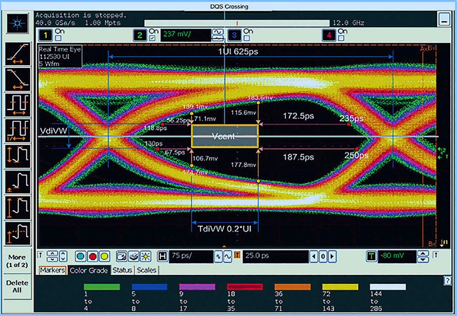
Jitter
Jitter is another form of soft error. It is the inevitable uncertainty in the way that electronic devices switch. We often discuss jitter under the general heading of signal integrity and there are a myriad of papers, textbooks, and courses built around measuring and predicting signal integrity in all types of communications networks.
For our purposes, because this chapter is looking at soft error in RAM systems, it is important when trying to find these elusive bugs that we are able to validate our noise and jitter margins. Keysight [11] discusses techniques for validating the integrity of DDR 4 memory systems using oscilloscope and logic analyzer-based measurements. Quoting the Keysight article,
Signal integrity is crucial for reliable operation of memory systems. The higher clock rates of DDR4 memory cause issues such as reflections and crosstalk, which cause signal degradation and logic issues.
With an oscilloscope, displaying a captured waveform as a real-time eye (RTE) offers insights into jitter within serial data signals. By showing when bits are valid (high or low), the RTE provides a composite picture of physical-layer characteristics such as peak-to-peak edge jitter and noise.
Getting full insights into the data-valid window and expectations of bit failure requires measurements of the worst-case margins in timing (tDIVW) and voltage (vDIVW). This is done using eye diagram mask testing.
The eye diagram referred to in the above quote is shown in Fig. 12.5.
Software-based memory errors
We’ve discussed software-based errors in memory in earlier chapters and there is no need to have a second in-depth discussion about them. However, it would be valuable to summarize some of the most common software bugs that can corrupt memory and crash a system or result in bad data. Fortunately, memory errors due to a flaw in the algorithm should be deterministic, if rare, and there are methods (previously discussed) to ferret out these bugs.
Many software errors are difficult to debug, particularly in programs written in C, because C gives the programmer direct access to memory where their code can make all sorts of mischief. This is great for performance and it puts the C code on par with assembly language in terms of efficiency. Typical memory errors include [12]:
- • Out-of-bounds array indexes.
- • Buffer overruns.
- • Dangling heap pointers (accessing a region of heap-allocated memory after the memory has been freed).
- • Dangling stack pointers (accessing a pointer to a local variable of a function after the function has returned).
- • Dangling heap pointers (dereferencing a pointer when the pointer points to a chunk of heap-allocated memory that has been previously deallocated via the free() function).
- • Uninitialized heap memory (heap memory is allocated using malloc() and some or all of this memory is not initialized before it is read).
- • Uninitialized local variable (a local variable of a function is not initialized before it is read).
- • The use of pointers cast from incorrect numeric values.
- • Vulnerabilities in coding that would allow data transfer overflows to overwrite other variables.
Fortunately, there is a rich set of software tools available from vendors that can be used to uncover these software defects if you take the time to learn them and use them before you deploy your software in your target system. And, as we’ve previously discussed in how to use the tools of real-time debugging, there are ways to find these flaws in software running in the target system.
When we add an operating system, as we’ve discussed, other memory defects may be introduced due to the interactions between the RTOS kernel, the hardware devices, and the separate tasks being simultaneously executed.
Concluding remarks
I’m writing this book on a desktop PC I built during the summer of 2019 for no particular reason other than I’m a computer geek at heart and I love to have the latest hardware. The system has an AMD Ryzen processor, 32 Gb of DDR 4 memory, and a 1 Tb solid-state drive. I mention this because I remember the first computer I ever built, a 6502-based system with 64 Kb of RAM using 1 K × 1 bit SRAM parts that I wire-wrapped together. I stored my programs on audio cassette tape. But it worked. I played games and wrote programs in Basic and assembly language and that computer started me on my path to this one.
In the years between then and now, I built or purchased more than 20 computers and each one was better than the previous one. My computer today has 500,000 times more RAM memory than the first 64 Kb system. In fact, I honestly considered buying four 16 Gb DRAM memory sticks just so I could have 64 Gb of RAM, or 1 million times more RAM than my first computer.
As we’ve discussed in this chapter, RAM is getting faster and smaller. Semiconductor technologies are pushing the limits that earlier device physicists thought we could never exceed. The FinFET technology is a good example of that. The dark side of the Forcee is that with the shrinking geometries comes more soft errors. These errors just occur and may occur so infrequently as to be impossible to analyze and correct. The only way to “debug” them is to accept that they are bound to occur with some probability and prepare a strategy against them.
For software, it would involve more defensive programming with rigorous bounds checking to raise the confidence level that the data values being recorded, transmitted, or used in calculations are sane ones.
For hardware, we already know to utilize watchdog timers to guard against an errant programming bug. I hope some of the debugging techniques described in this chapter will provide some insight for how to approach resolving memory issues.
Also, because this is the last chapter, a few more general remarks might be in order. When I was thinking about writing this book, I had two goals in mind:
- 1. Teach students and new electrical engineers the process of how to find and fix defects in a timely manner.
- 2. To make the neophytes as well as the seasoned pros, aware of the vast array of literature written by equally seasoned pros, on how to take maximum advantage of the tools that their companies offer.
I’ve written many of these articles myself in my employment history with HP, AMD, and Applied Micro Systems. My whole professional career has been deeply embedded in test and measurement, with a little materials science at the front end and education at the back end.
Manufacturer’s applications notes and white papers are treasures of great information about getting the most out of their tools and on ways to solve gnarly problems. Yes, there is marking fluff embedded in the app note, but there is great information there as well. With the Internet at your fingertips, any app note or white paper is a few Google searches away.
Thanks for reading this.