
4: Best practices for debugging embedded hardware
Keywords
Debug; Hardware; Process; Design review; Testability; Test plan; HW/SW integration; Lifecycle; PCB design; Ground management
Introduction
I feel more comfortable writing this chapter because I was a hardware designer at HP before I was promoted to management and became a generalist.a I also teach microprocessor design at the University of Washington Bothell and the senior level students in my class must complete a design project in the class, complete with a printed circuit board (PCB) that they have to design. For most of the students (except those whose hobby is electronics), this is their first foray into PCB design.
Later, they must complete a more substantial project as part of their Capstone Experience. All accreditedb EE programs are required to have a Capstone project as a required element in their degree programs. Our Capstone model has the students function as a small consulting engineering company [1]. This exposes our students to the entire product design lifecycle, including hardware turn-on, debugging, and validation testing.
I also manage the Capstone program for our department and have personally been the faculty advisor to many teams. I’ve probably observed more wrong ways to debug hardware that you can imagine. The inability of a student to logically analyze a problem, form a hypothesis of the cause, then test that hypothesis causes them to waste valuable time and destroy parts and printed circuit boards in the process. Observing these students was my primary motivation for deciding to write this book.
As in the previous chapter, this chapter will focus on best practices. Once again, I’ve culled the literature to find tips and tricks as well as application notes from the companies that provide the tools of the trade for the hardware designer.
The debug process for hardware
I want to kick off this chapter by relating a story that was told to me during the years I served on the Project Management Council in Corporate Engineering at Hewlett-Packard. I also told this story in an earlier book [2], but its lesson is still relevant today.
About 20 years ago, the part of HP that is now Keysight® was rapidly moving towards instrument designs based upon embedded microprocessor. HP found itself with an oversupply of hardware designers and a shortage of software designers. So, being a rather enlightened company, HP decided to send willing hardware engineers off to software boot camp and retrain them in software design. The classes were quite rigorous and lasted about 3 months, after which time one of the retreads returned to his HP division and started his new career as a software developer.
This “retread engineer” became a legend. His software was absolutely bullet-proof. He never had any defects reported against the code he wrote. After several years he was interviewed by an internal project team, chartered with finding and disseminating the best practices in the company in the area of software quality. They asked him lots of questions, but the moment of truth came when he was bluntly asked why he didn’t have any defects in his code. His answer was quite straight-forward, “I didn’t know that I was allowed to have defects in my code.”
In hindsight, this is just basic Engineering Management 101. While he may have been retrained in software methods, his value system was based on the hardware designer viewpoint that defects must be avoided at all costs because of the severity of penalty if a defect is found. A defect may render the entire design worthless, forcing a complete hardware redesign cycle taking many months and costing hundreds of thousands of dollars. Since no one bothered to tell him that it’s OK to have bugs in his code, he made certain that his code was bug-free.
My point here should be obvious. Hardware is unforgiving and it is potentially very expensive to find and fix defects. We’ve made great strides in technology since then, particularly in the area of FPGAs where reprogrammability has turned much of hardware design into software design. However, you can’t do everything in an FPGA. At some point, the signal must exit the FPGA and interact with the outside world or other software. Sometimes it interacts too strongly and then a perfectly performing system can’t be shipped because its RF emissions are too great to allow it to be sold as a commercial product.
Design reviews
My number one recommendation for best practices in the category of “the easiest defects to find are the ones that aren’t there” is to have other engineers review your work in the hope of finding problems before they become embedded in an ASIC or PC board. I teach my students how to do a design review in the faint hope that they will take my advice, but this is like trying to spit into the wind. The typical response is, “We didn’t have time to do a design review.”
The alternative behavior is for a student to come into my office and ask me to do a quick design review because they need to order their PCB in the next hour or so. Even worse, they show up with a PCB layout drawing and no schematic diagram of the circuit. They never bothered to do a schematic design.
A sane organization realizes the value of design reviews and makes certain that all project schedules contain time for engineers to have design reviews of their hardware and to have the time to serve on design reviews as examiners for other engineers.
We all know that the later into a project a defect is discovered, the more costly it is to fix the defect. This is true for software and for hardware, but more and more software (and FPGA-based hardware) can be repaired in the field with software updates, so perhaps this general rule is not as universally true today as it once was, but not every embedded system lends itself to field upgradability. Still, as a manager, would you prefer to have your engineers designing new products or repairing products that are out in the field generating customer complaints?
My very first hardware design review was an extemporaneous meeting between me and David Packard, the “P” in HP. I was fortunate to have started working at the Colorado Springs Division of Hewlett-Packard when both William Hewlett and David Packard were both alive and very much in charge of the company. They were at our division for the annual division review and “Dave” was wandering around the R&D lab talking with the engineers.c
I was working on a schematic design, not paying much attention to what was going on around me when a shadow suddenly appeared over my desk. I looked up to find that David Packard was standing over me looking at the schematic. He pointed to a part of the circuit and said, “That won’t work.” I said, “Yeah, it will.” That was his way of introducing himself.
Several years later I was at HP corporate headquarters in Palo Alto and I happened to be walking down a hallway and I ran into him. I said hello and introduced myself, and I reminded him of our first design review meeting. He smiled, but I don’t think he remembered the meeting with the same clarity that I did, and still do.
Anyway…
What are the steps for a good process for a design review? A note here that the purpose is to uncover flaws and weaknesses, not rubber stamp a design so that a box could be checked off saying that you held a design review. A design review is labor-intensive, takes time and is very expensive in terms of lost productivity. When you take an engineer away from their own design work, there is a double whammy because the actual hourly cost of an engineer, including salary, benefits, equipment, etc., and on top of that, the lost productivity cost to their primary project becomes the cost of doing the design. Therefore, for a design review to have a positive return on investment (ROI), it needs to be effective and taken seriously by everyone involved in the process.
Step 1: About a week before the review, identify three or four other engineers who will take part in the review. Ideally, one of the engineers will be the moderator/recording secretary and the others will do the actual review of your design.
Serving on a review panel is like jury duty. You can get out of it once or twice with a good excuse, but you eventually must take part.
Step 2: Circulate all the pertinent design documents at least 3–4 days before the review. This would include schematics, data sheets, and ABEL, CUPL, VHDL, or Verilog code for the programmable parts as well as timing calculations, simulation results, data sheets, or app notes. In short, any of your design documentation should be part of the review material.
Step 3: To start the review, the engineer gives a brief overview of the design and covers the pertinent product requirement specifications. This might cover the choice of microprocessor or microcontroller being used, the amount of memory needed, clock speeds, and so forth.
Step 4: During the review, the moderator will lead the review process and the reviewers will bring up any design issues that need further attention. The purpose of the review is to identify issues, not to solve them. However, engineers being engineers, getting into a problem-solving mode is almost inevitable.
The designer being reviewed may offer some explanations but should not attempt to defend the design in the review. This also brings up another issue. The reviewers should comment on the design, not on the designer. Saying something like, “How could you make such a bonehead mistake?” just puts the designer on the defensive and the effectiveness of the review will quickly unravel.
The moderator notes each issue as it comes up, and whether it needs further follow-up by the designer. If the designer does not agree with the comment, defending the choice should be reserved for a later date.
Step 5: At the conclusion of the review, the moderator reiterates each issue that requires further attention and the meeting adjourns.
Step 6: The moderator then writes a summary of the meeting contents and the issues to be addressed. A copy of this report is sent to the lab manager and all the participants.
Step 7: The engineer whose design was reviewed then addresses each issue and does a final write-up report of how each issue was addressed. Sometimes, a follow-up review is scheduled if the number of issues was significant and the design was substantially changed.
Step 8: Once everyone signs off on the review, the design can move to PC board layout.
I can remember the details of my first HP design review like it was yesterday. I was very nervous because I was going to be reviewed by some of the top guns in the lab and I was the new guy. My design was a controller board for a 16-channel oscilloscope probe multiplexer with a 1 GHz plus bandwidth (HP 54300A).
During the review, one of the reviewers picked up on some high value resistors that were connecting the 8 data lines to the + 5 V power rail and to ground, seemingly at random. I told him that was for testing and the release version would not have the resistors loaded. The purpose was to force the data lines to always supply the processor with an NOP (no operation) instruction so I could probe the board and look at timing margins and signal integrity. He told me, “That’s a cool idea. I should try that.” I was very relieved.
There is an epilogue to this event. Years later, after I had left HP, I ran into one of my colleagues from the R&D lab at an Embedded Systems Conference. We were reminiscing about old times and he mentioned that my probe multiplexer had a very high failure rate, which I couldn’t understand. The problem turned out to be the high-frequency transmission line switches that I had chosen to use. According to the manufacturer, they were rated for several million cycles, which should have been more than enough in service.
However, these switches were originally designed to be used in missiles where they had to be reliable for a few hundred switches, and then they disappeared in the ensuing explosion. The manufacturer had never tested the switches to failure, and the failure rate quoted was only a guess. The design review would not catch this defect, but a more thorough investigation of the switch data, or the manufacturer of the switch, might have raised a red flag.
Bob Pease [3] was a legendary analog circuit designer at National Semiconductor (now part of Texas Instruments). In his classic book on troubleshooting analog circuits, he describes how he also conducts informal design reviews.
At National Semiconductor, we usually submit a newly designed circuit layout to a review by our peers. I invite everybody to try to win a Beverage of Their Choice by catching a real mistake in my circuit. What we really call this is a “Beercheck.” It’s fun because if I give away a few pitchers of brew, I get some of my dumb mistakes corrected. Mistakes that I myself might not have found until a much-later, more-painful, and more expensive stage. Furthermore, we all get some education. And, you can never predict who will find the picky little errors or the occasional real killer mistake. All technicians and engineers are invited.
Test plan
The primary audience for this section is the soon-to-graduate EE student. Assuming that your resume is sufficiently compelling, a company will phone screen you and then if you pass that hurdle, invite you in for an in-depth interview. Along with the invariable technical interview, you’ll probably interview with several of the managers. Their job is to assess your “other skills.” This would normally include things like professionalism, communications, match to company culture, and maturity level.
Your job is to convince the interviewers that you are the best candidate for the job. Along with your technical ability, you need to convince them that you are ready to step into the maelstrom and be productive from day 1. They will invariably ask you about projects you’ve done and from speaking with our alumni,d we’ve learned that their Capstone Experience was one of the key factors in their getting hired. What impressed the interviewers was the “soft skills” that the students learned as part of the Capstone project. Skills such as tracking schedules, holding team status meetings, documentation, and having a test plan. The test plan is a real winner with interviewers.
The test plan is the roadmap that you will use to go from a raw PCB to a functioning prototype. Just like a pilot’s checklist, it is your step-by-step guide to turn on and debug so that you do not miss anything, or worse, waste time and destroy your hardware.
We give every new Capstone team an official lab notebook, just like the ones I had as an engineer. They are instructed to create the test plan and then document their work in the lab notebook. This is an unbelievable hardship for the generation of students who have a smart phone surgically attached to their hand, but they humor me because I have the power of the grade to hold over them.
To introduce the topic to the students, I pose this question.
Suppose that you’ve just gotten your raw PCB back from the board manufacturer. It’s gorgeous. It is the first PCB that you’ve ever designed. What is the first test that you perform on this board?
After the blank stare goes away, I get a variety of answers, but rarely the correct one.e
Here is the format that I suggest for the test plan. Your mileage may vary.
- 1. Raw Board
- a. Visually inspect raw board and compare with design
Match/Problem?___________________ - b. With ohmmeter, measure resistance between Vcc and ground
Expected: Open circuit, measured_____________
- a. Visually inspect raw board and compare with design
- 2. Loaded board
- a. Are all parts properly located and aligned?
- b. Are all socketed IC pins in the sockets and are the ICs oriented correctly?
- c. Are all the leads soldered to the board?
- d. Are there any solder bridges between pins?
- e. Is there any residual solder flux on the board?
- f. Are all the components seated properly?
- 3. Board turn on (no external inputs)
- a. Measured resistance between Vcc and ground__________________
- b. Is it a short circuit? Yes/No________
- 4. Apply power with current limit turned on or a series resistor in the power rail
- a. Any odors? Yes/No__________
- b. Any heat? Yes/No___________
Note: This test implies that you’ve made a worst-case power consumption calculation at idle, so that if the board exceeds this during turn on you know something is amiss before one of the traces turns into a fuse. - 5. Measure supply voltages
- a. Is Vcc correct on all inputs? Yes/No_______
And the list goes on. At each step, you are gaining confidence that your design is correct.
And so forth. While this may seem a waste of time, it is worth its weight in time saved and it definitely impresses your interviewers.
The test plan really becomes valuable when something doesn’t measure what it should. Here’s a simple example. Suppose you are designing a precision rectifier circuit. You apply a 1 kHz sine wave and observe on the oscilloscope that during the negative transition of the input, the rectified sinewave output, is missing.
An experienced designer would head straight for the rectifying diodes, realizing that one is probably soldered in backward or there is an error in the PCB connection. Maybe the silkscreen layer on the board is wrong. Whatever.
The best practice that I teach my students is to stop and write down in their lab notebook what they expected to see and what they observed. Because our oscilloscopes are connected to the network, I encourage the students to print out the display trace so that they can add it to the notebook.
Step #2: I tell them to think about how the circuit should work (theory of operation) and based upon their understanding of the circuit, write down several possible culprits. This will force them to reinforce their knowledge of the circuit behavior before they attack the board.
This is particularly true when a student grabs an example circuit off the web and tries to use it without really understanding how it works. If necessary, reread the data sheet(s) to make sure that you haven’t missed something.
Step #3: Probe the board with the oscilloscope and note the waveforms and DC operating points at the circuit nodes.
Step #4: Run their design in a simulator, such as Spice, LTspice, or Multisim and try to recreate the fault by testing their hypothesis in simulation. Once they can demonstrate that the simulator will produce the same output as their circuit, then they may proceed to investigate the suspected part.
If you are an experienced hardware designer, at this point you are probably rolling your eyes. I know what you’re thinking. But…
There are many years between you and that new engineer. Let’s give the newbie every opportunity to be successful.
Design for testability
Way back in the Dark Ages, I wrote an article [4] about designing embedded hardware with an eye to tools that will be needed downstream to debug the system. Because I was involved in the design and manufacture of in-circuit microprocessor emulators (ICE), this was my primary focus in the article.
It was basically simple stuff, such as avoiding the positioning of the microprocessor in such a way that connecting an emulator or logic analyzer is impossible. Whenever you look at a marketing brochure, you see a single board sitting conveniently on an immaculately clean desktop with the instrument of interest prominently displaying an exciting waveform.
In reality, the real board is going to be crammed into a card cage with barely enough space for airflow. If you do need access to the processor for debugging, it will likely be a JTAG connector that you need to plug into. It won’t do you any good if the connector is located on the side by the backplane socket or guide rails, and not the side by the board ejectors.
Along the same lines, design the first board as a prototype board, not as your final board. Give yourself a fighting chance to find problems.
Although Pease’s book was dedicated to analog circuitry and discussed a fair amount about IC design bugs, there is a lot of practical information in it that is still useful today. In a section titled “Make Murphy’s Law Work for You,” he describes how he often allocates some extra space in certain parts of his PC board because he isn’t 100% sure that it will work, so he’s leaving room to make modifications in the next revision of the board.
Another really interesting tip I learned from reading his book is something that only an analog designer would think about but digital designers tend to ignore, which is signal fidelity. Pease was describing looking at a pulse train that had a lot of ringing in it. Because he was concerned about the fidelity of the pulses, he investigated it and found that the 6″ ground lead from his oscilloscope probe was producing the ringing. He fixed the problem by adding small ground pads near critical signal nodes that he wanted to probe.
Thus, using a probe with a ground ring close to the tip of the probe, as shown below in Fig. 4.1, he was able to eliminate the ringing caused by the inductance of the 6″ long ground wire clip.
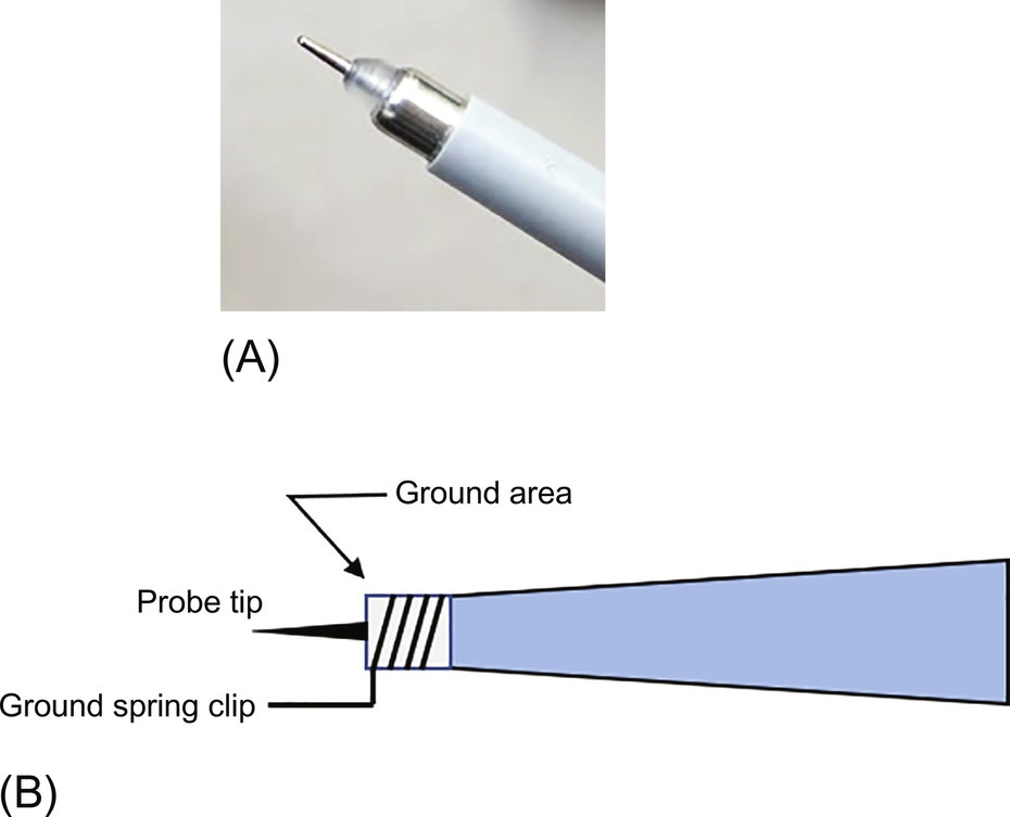
I like to add through-hole pads in critical traces. The hole is sized so I can solder a small post to it and attach a probe. Also, it is almost absolutely required that you add ground pins and even Vcc pins, just in case you need to power a logic probe to examine the circuit.
Have a process
Here’s where hardware and software part company. Software can easily be checked by a recompile and download cycle, assuming that you don’t have an overnight software build process to deal with. One of our claims with the HP 64000 in-circuit emulator system was that you could find a bug, fix it, and download a new software image in under 1 min. That’s great marketing fluff, but it isn’t a process either.
Putting that aside for a moment, we don’t have the same luxury with hardware because hardware is physical and not ethereal. Before we start swapping components, cutting traces, or hanging filter capacitors on the circuit, we should have a high confidence level that the fix will work.
I think I discussed this point in every one of the preceding chapters, so hopefully it will stick. Like software, there are best practices for designing the hardware that you should follow in order to minimize the likelihood of introducing a defect into your design, or at least minimizing its severity.
Unless you’re designing an FPGA, your objective is not to introduce a defect, just like the HP engineer in the example I cited earlier in the chapter. However, your process should include in your process plan the reality that you will likely have to do one or more circuit redesigns before the hardware is ready for prime time.
Also, because this is a design that will need to be integrated with software, we need to consider the very likely scenario that the hardware will check out just fine until the actual software is introduced, and then, and only then, will the bugs come to light. So, the process usually requires that there be an iterative aspect to the hardware debug phase.
Embedded system tool suppliers have been discussing this process for years and I have been as guilty as the next marketing drone because I spent a total of 19 years working for tool companies.
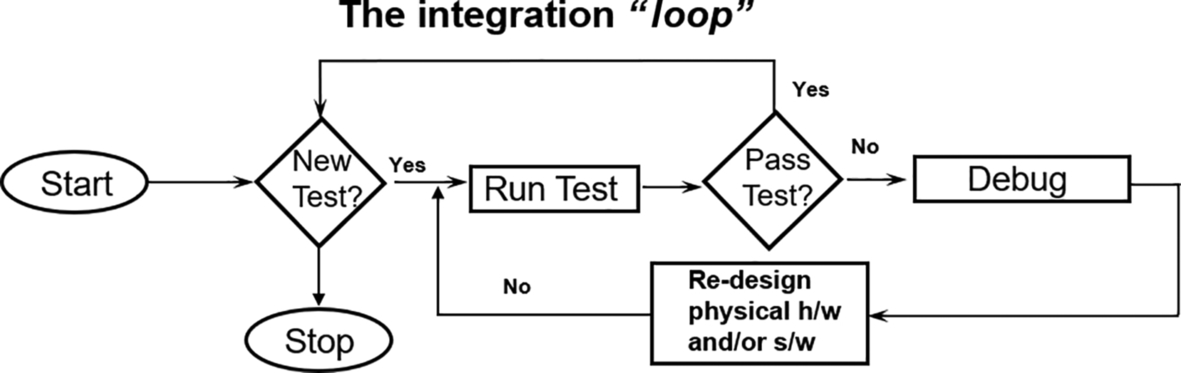
Here’s the classic hardware/software (HW/SW) integration loop figure:
This flowchart describes the classic HW/SW integration process. Many people have argued that this chart is either misleading or it encourages bad practices because it is implying that the hardware and software are isolated from each other until the very moment when they are brought together, late in the product design cycle, and then integration can begin.
While Fig. 4.2 is conceptually easy to understand, it is considered to be rather backward. In fact, various experts would argue that HW/SW integration, test, and debug is an ongoing process and bringing the final versions together should be an anticlimax rather than a cataclysmic event.
There are lots of reasons why the HW/SW integration process is a major time suck to the product development schedule. However, assuming that the hardware works as the designer intends it to work, and the driver software works as the firmware designer intends it to work, then what’s the problem? I would posit that a communications failure between the HW and SW developers accounts for the vast majority of the problems with the integration phase of the project.
Here’s a simple example. The hardware designer ignored the Endianness of the system because all that needed to be done was to connect the peripheral devices to the address and data buses. Murphy’s Law dictates that whatever the Endianness that the firmware developer assumes, it will be the opposite. Sometimes it is an easy fix because the processor has a register that enables the Endianness to be software-controlled. In the ARM 8 Cortex processor, the Endianness of the data can be set via a software register, but instruction accesses are always Little-Endian.
Certain compilers such as GCC will allow you to set an Endianness switch, so the bug fix might only require a recompilation of the code. Still, a bug is a bug.
If a process was in place to address this possibility, then the internal formal specification for the product would spell out the Endianness of the system and software developers could build hardware simulation code that takes this into account. An important process requirement that could minimize the need for the HW/SW integration phase is to agree early on that the software team and the hardware team come together and create a detailed interface specification so that the software team could create a testing scaffold for their code that would provide a correct interface to the hardware under development.
Many RTOSs, such as Integrity from Green Hills Software,f have extensive support for hardware virtualization so that the software team can move forward with code development and integration with the RTOS while hardware is still under development. So, there really isn’t a good excuse for not modeling the hardware so that incremental integration can take place.
David Agans wrote a very readable book on debugging [5]. He suggests a process that you can get in the form of a poster. Fig. 4.3 is a reproduction of this poster. I suggest that you put it up in your lab to remind yourself how to proceed, just in case you forget.

This is a wonderful little book and an easy read. You can easily finish it at a long session at Starbucks. In granting me permission to reproduce the poster, the author asked that I recommend the book, and I do recommend it. It has lots of practical suggestions and real examples from the author’s embedded systems design experience.
Of the nine rules, the one that resonates for me is the last one, If you didn’t fix it, it ain’t fixed.” Because I minored in English, I would say, “it isn’t fixed,” but the sentiment is the same.
It might be really tempting to ship a product with a bug that you’ve seen but can’t seem to isolate. It’s infrequent, so what’s the harm? But you know it’s there, it’s lurking.
You might try to convince yourself that it was a glitch, or a hiccup, and it isn’t “really” a bug, but in your heart, you know it’s there, so you might as well find it.
However, suppose that management needs the product to ship and you are feeling the pressure to release it to manufacturing knowing that there is a defect in the product. How do you respond? This dilemma has been much studied, with the Boeing 737 MAX incident as only the latest to make the news. The IEEE website has a page on the Code of Ethicsg that should provide you with some guidance:
to hold paramount the safety, health, and welfare of the public, to strive to comply with ethical design and sustainable development practices, and to disclose promptly factors that might endanger the public or the environment…
My first job at the Colorado Springs Division of Hewlett-Packardh was as a CRTi designer. I was responsible for the CRT in the HP 1727A storage oscilloscope. Today, any modern oscilloscope is a storage scope because the waveform acquisition system is all digital. In the HP 1727A, an electron beam “wrote” the waveform on a dielectric mesh. Writing involved knocking electrons off the mesh, creating local areas of positive charge wherever the beam struck the mesh.
A second low-energy electron beam then flooded the mesh and any of those electrons that came close to the positively charged regions were able to get through the mesh and then were accelerated with a 25 kV potential to the phosphor-coated screen, producing the stored image of the waveform. Anyway…
The scope had a bug. This is strictly an analog design. No processor in it, but it still had a bug. The bug was infrequent, and we could never find it. The bug was in the trigger circuitry that would cause the electron beam to fire once and record the waveform. Occasionally, for no apparent reason, the oscilloscope would trigger, but apparently the trigger signal did not come from an input source.
Now, the whole point of buying this $20 K + instrument was to be able to capture elusive signals. It rather defeats the purpose if the instrument randomly fires and the customer never sees the real signal they were hoping to find.
For some reason, the engineers began to suspect that it was “microphonics,” or mechanical jarring, that was causing the scope to misfire. So, we started to hit it with rubber mallets and drop it. Anything we could think of to reliably generate the fault, we tried, and we couldn’t reliably recreate the failure. I think they eventually found it to be a high-voltage arc that found its way to the trigger board, and the problem was resolved.
To their credit, they did not ship any of these instruments until the problem was solved.
Know your tools
My involvement in embedded systems has always been on the debugging tool side of the industry, so I am understandably focused on this dimension of the process. One of the biggest issues that I saw and experienced many times over was the inability of our customer to understand how to properly use our tools for maximum advantage.
I’ve seen it with really senior engineers and with my students. Of course, we the tool vendors have to share some of the blame because we’re the ones who created the tool and then did not provide adequate documentation to make it easy to understand how to use the tool to its fullest extent.
In the introduction to the book, I mentioned Hansen’s Law. However, because most people never read the introduction, let me summarize it again. John Hansen was a brilliant HP engineer whom I had the privilege to work with in the Logic Systems Division in Colorado Springs. He said,
If a customer doesn’t know how to use a feature, the feature doesn’t exist.
It’s a very simple yet extremely insightful statement about designing complex products and the need to be able to simply convey their usefulness to an end user.
In his seminal book, Crossing the Chasm [6], Geoffrey Moore looks at the marketing of high-technology products. Moore identifies a fallacy in the traditional way that high-technology markets are modeled. Consider the traditional life cycle model for the adoption of a new product in the marketplace, shown in Fig. 4.4A. We see each segment of the market occupying a portion of the area under the bell curve. The area in their segment represents the potential sales volume for that market. I think we can easily identify the characteristics of each segment.

However, for the successful marketing and sales of new technology-based products, Moore argues that this model is wrong. He argues that there is a fundamental gap, or chasm, that exists between the early adopters and the early majority. Referring to Fig. 4.4B, we see that the segments comprised of the early and late majorities are the bulk of the market. Therefore, while initial sales to the “techies” might be very gratifying, those sales can’t sustain a successful product for very long.
Moore says that the early majority are the gatekeepers for the rest of the market. If they embrace the product, then the product can continue to grow in sales and market impact. If they reject it, then it will die.
In order to be accepted by the early majority, there are several key factors that must be in play, but I’ll just zero in on two factors that I think are germane to the point I’m trying to make.
- • The early majority tends to seek validation of a product’s value by seeking the recommendation of other like-minded members of the early majority whose judgment they trust.
- • There must be a “complete solution” available for the product.
The second bullet is the one that is relevant here.
As developers of new technology, we are constantly coming out with newer and better solutions to meet the needs of our customers, who are themselves developing new and innovative products. These customers, the early majority, don’t have the time or desire to put up with the glaring omissions of a new product’s support infrastructure. Manuals with errors, lack of technical support, training are all unacceptable show-stoppers for the early majority.
So, what’s this got to do with “know your tools?” We, the R&D engineers, can provide all the features in the world to make our in-circuit emulator or logic analyzer more compelling, but if a customer can’t take advantage of the feature set because it is too difficult to learn, or they don’t have the time to learn, then the tool is not what they need.
Yes, the tool manufacturer needs to bring every technology transfer best practices to bear to make the features of their products accessible and easy to understand. In their defense, I will say that the tools today are much better than when I was working in the field. This is primarily due to the additional processing power built into the tools and the amount of memory that even the most modest of instruments carries within. Rather than trying to find it in the manual, I can press a context-sensitive help button and see the manual page that I need to access.
But… the onus is still on me to devote enough time to learn the tool. If I’m always too busy to learn how to take advantage of my tools, then I have no one to blame but me for not surviving the next round of layoffs. Just remember the parable about the wood cutter who was always too busy chopping down trees to sharpen his axe and then couldn’t understand why he was not able to cut as much wood as he needed to.
Understanding your tools extends beyond a knowledge of how to use the feature set. It also includes an understanding of how the tool interacts with the environment that it is being used in.
In my Introduction to electrical engineering class (Circuits I),we cover the topic of the D’Arsonval meter.j For those readers who never used an analog multimeter, the basic meter consisted of a meter movement that could deflect to the full scale of its range with only microamperes of current flowing through the meter coil. So, for example, if you have an analog meter that will deflect full scale with 10 μA of current and you place that meter in series with a 10 MΩ resistor, you now have a voltmeter that can measure 10 V full scale with a 10 MΩ input resistance. Of course, the meter’s windings also have a resistance that usually is part of the circuit calculation. The point of this lesson is to sensitize the student to the interplay between the circuit under observation and the tool being used to observe the circuit.
Another exercise that we go through in class is the difference between accuracy and resolution. Your digital multimeter may be able to resolve the voltage down to ± 1 mV, but the accuracy of the meter may only be trustworthy down to ± 15 mV on the 10 V range. As experienced engineers, we know this, but students constantly fall into the trap of accepting without question the reading on the meter.
Oscilloscopes can also be a significant perturbation to a circuit as well as a source of error in their own right due to the differences in bandwidth among the probes. I recall a student asking me why the signal amplitude of a pulse train was so low. I poked around and sure enough, the pulses should have had an amplitude around 5 V, but the scope registered below 500 mV.
I then started looking at the scope setup and I noticed two things:
- 1. The scope input was set for 50 Ω.
- 2. The probe was set at 1 × attenuation.
In effect, when the student probed the circuit node, he was hanging a 50 Ω resistor to ground on the node.
This is all part of the educational process and it is why labs are such important parts of an engineering student’s education, even though they tend to complain about the time they have to spend in the labs. I often wonder if metrology should be a required course in an EE’s curriculum rather than an elective course. In lecture, the students could learn the theory of measurement and their lab experiments could demonstrate the practical side of measurement instruments, such as the proper way to use them and how to understand and interpret the results.
On the digital side, the logic analyzer has always been the premier measurement tool, although that dominance may be waning (more on that in a later chapter). However, the logic analyzer (LA) can be a very intimidating instrument to learn the basics on and even more intimidating to learn how to use it to solve the really tough problems.
Trying to observe 100 or more signals going in and out of a surface-mount integrated circuit with pin spacings of 0.5 mm and clock rates of 500 MHz is not something that you can do by clipping 100 flying leads to the IC. In these situations, the measurement tool is an integral part of the system and the system must be designed from the start with the logic analyzer interface designed into the hardware. Typically, this will require that the first PC board be a “throwaway” and only used for development. Fig. 4.5 [7] illustrates the necessity of planning ahead.

This circuit adapter provides 16 input channels and 100 kΩ isolation (see equivalent load diagram in the lower right). This probing solution is recommended for normal density applications (parts on 0.1 in. centers) and where speed is not a significant issue. Keysight offers additional probing solutions and detailed application literature for probing high-speed and high-density circuits. The Keysight probes are also designed to mate to high-density surface mount connectors made by Mictor and Samtec.
However, in most cases, these solutions also require that the probing adapter be built into the PCB and be part of the planning process from the outset. Once the circuit is thoroughly debugged and characterized, the probes can be removed in the next revision of the board.
Microprocessor design best practices
Introduction
Like software, the easiest bugs to fix are the ones that aren’t there. In other words, the fewer bugs that you, the designer, designs into the system, the higher the likelihood that you can confidently blame the firmware designer for the bug (Sorry, I couldn’t resist). So, in no particular order of importance or relevance are some guidelines that I teach my students in their microprocessor system design class.
If you are an experienced digital hardware designer, these rules are burned into your consciousness, or maybe they aren’t. In any case, if you find these hints too elementary, just skip to the next chapter. I won’t get angry, I promise.
Design for testability
Yes, I’ve said this before, but I can’t say it enough. Design your boards so that they are testable. Bring critical signals out to easily accessible test points and liberally sprinkle the board with ground pins or pads that you can easily access. As described in the previous section, you may need to provide accessibility for other debugging tools, such as logic analyzers or JTAG ports.k
As you design for testability, keep in mind the perturbation that your measurement tool may have on circuit behavior, such as additional capacitive loading. One workaround is to provide a buffer gate or transistor to isolate the signal that you want to probe.
Fig. 4.6 illustrates this point. A buffer gate is being used to isolate an oscilloscope probe from the circuit. While it does address the issue of circuit loading, it adds an additional part and potential loss of synchronization (clock skew) due to the propagation delay through the buffer gate.

Consider PCB issues
The PC board does more than simply hold the components and interconnect them. The board can become part of the system in a way that is analogous to the role of measurement tools. The board can be a perturbation on the system and the part it plays generally needs to become part of your solution. Another point to consider is that your circuit may work during initial testing, but anomalies may not turn up until much later. One of a hardware designer’s biggest nightmares is a circuit glitch that won’t appear again for weeks, but you know it is lurking.
When cost is a major consideration, PCBs may only have one or two layers, which then puts a premium on ground and power bus management. Generally, high-speed signals want to travel over ground planes so that a constant impedance transmission line is created. However, a four-layer board with inner layer power and grounds will cost significantly more.
You will need to consider the static and dynamic electrical properties of the signal traces on the board. Obviously, the current carrying capability of the trace is important. These you can readily find online in tables from the PCB manufacturers’ web sites. The thickness of the copper trace is not specified as a thickness of the copper layer (that would be too straightforward). Rather, it is expressed as a weight of copper 1 ft2 in area. The most common copper thickness is 1 oz. copper, which translates to a thickness of 1.4 mils (0.0014 in. or ~ 35 μm), although 2 oz. layers are also used.
If you want to calculate the correct trace width for a given current through the trace, you can use the formula:
R(ohms)=ρ⁎L/A
where ρ is the electrical resistivity of copper, measured in units of ohm-cm; L is the trace length in cm; and A is the cross-sectional area of the trace in cm2. At room temperature, ρ = 1.68 μΩ cm. This is noteworthy because the temperature coefficient of the electrical resistivity is positive. The resistivity goes up as the temperature goes up. This means that it is possible to end up with a positive feedback loop that turns a trace into a fuse if the current load is too great, even for an instant.
Dynamic effects add another layer of complexity. Now we need to consider the PCB material and thickness as another determining factor. Also, transmission line effects become an issue while electromagnetic interference (EMI) also comes into the equation.
I’m not an RF expert, so I’ll just discuss what I’ve learned through having to deal with some of these issues in the past. If a fast signal is going to go to an off-board connector, such as a 50 Ω BNC or SMA connector, then it makes sense to match the impedance of the microstrip transmission line (your PCB trace) to the impedance of the cable it’s driving. In order to.
The only time I ever had to deal with this issue was when I was taking it in a class, but then again, I’m not an RF designer. Nevertheless, let’s consider a trace on a typical PC board material (FR4) and the trace is above a ground plane, as shown in Fig. 4.7.
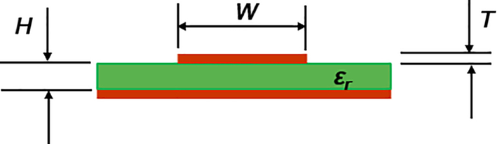
Here:
- H = Thickness of the FR4 layer above the ground plane.
- W = Width of the trace.
- T = Thickness of the trace.
- ɛr = Relative permeability of the FR4.
The equations of interest are as follows [8]:
The characteristic impedance,Z0(ohms)=87√ɛr+1.41ln(5.98H0.8W+T)

The distributed capacitance,C0(pFinch)=0.67(ɛr+1.41)ln(5.98H0.8W+T)
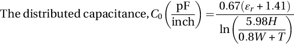
The propagation delayTpd(psinch)=C0×Z0
I asked a colleague on the UWB faculty who is an RF specialistl to choose the correct impedance for a PCB trace that will be carrying a fast digital signal. I was curious if it was arbitrary or if there was an underlying engineering principle. I’ll try to synthesize his answer as follows: The goal is to avoid a situation where a pulse, such as a clock signal pulse train, interferes with subsequent pulses. This would be the case if there is a reflection at the load end of the trace and then a second reflection back at the transmission end of the trace.
The impedance of the microstrip trace should be set higher than the output impedance of the transmission gate and also at a value that would not cause the interference phenomenon just described. Thus, the transit time of the signal depends upon the length of the trace and the velocity of the signal, and the velocity depends upon the impedance. So, by adjusting the impedance, we can avoid degradation of the signal integrity due to reflections.
A typical value of the relative permeability of the FR4 PCB material is 4.4, but it can vary somewhat due to variances in the manufacturer’s formulation. However, we’re not quite done yet because ɛr varies with frequency. Fig. 4.8 shows the variation in the real part of ɛr with frequency [9].
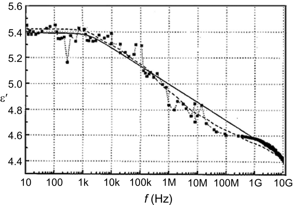
Referring to the figure, we can see that the frequency-dependent variation in ɛr means that the pulse will become more distorted as it travels down the trace because the speed of the Fourier components with be different and the impedance seen by each frequency component will be different.
The high-speed signals can also be attenuated along the trace because of losses due to the skin effect and in the dielectric. The higher-frequency components will be attenuated to a greater degree than the lower-frequency components. Therefore, as frequencies go higher, we need to consider other board materials such as Teflon or ceramics.
We also need to consider the reality that in a typical microprocessor-based system, we have many high-speed traces traveling in parallel over some distance. According to IPC-2251 [8]:
Crosstalk is the transfer of electromagnetic energy from a signal on an aggressor (source or active) line to a victim (quiet or inactive) line. The magnitude of the transferred (coupled) signal decreases with shorter adjacent line segments, wider line separations, lower line impedance, and longer pulse rise and fall times (transition durations).
A victim line may run parallel to several other lines for short distances. If a certain combination and timing of pulses on the other lines occurs, it may induce a spurious signal on the victim line. Thus, there are requirements that the crosstalk between lines be kept below some level that could cause a noise margin degradation resulting in malfunction of the system.
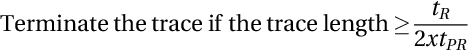
Hand in hand with the design issues we’ve examined is the consideration of whether to terminate a trace on the PCB in its characteristic impedance, Z0. Here’s a good rule of thumb:
where
- tR = Pulse rise time or fall time, whichever is fastest,
- tPR = Propagation rate on the PCB, typically about 150 ps/in.
For a pulse with a rise time of 500 ps, the trace should be terminated if it is longer than about 4.25 cm.
There are several ways to terminate a trace in its characteristic impedance, and you can find resistor packs designed exactly for that purpose. According to an applications note from TT Electronics [10]:
Multi-gigabit per second data rates are now commonplace in the worlds of telecommunications, computing and data networking. As digital data rates move beyond 1-Gbit/s, digital designers wrestle with a new list of design problems such as transmission line reflections and signal distortion due to poorly selected transmission line terminators. By properly choosing a termination matching the characteristic impedance (Zo) of the transmission line, the energy in a digital transmission line signal can be turned into heat before it reflects and interferes with other forward propagating signals.
The selected type of termination is crucial to the signal integrity of high-speed digital design. In ideal designs, parasitic capacitance and inductance can kill an otherwise well-thought-out high-speed design. Care must be taken, however, when choosing a resistor for high speed transmission line termination – not just any resistor from the top desk drawer will do. A terminating resistor that matches Z0 at low frequencies may not remain a match at high frequencies. Lead and bond wire inductance, parasitic capacitance, and skin effect can drastically change the impedance of a terminator at high frequencies. This change in impedance, and the resulting signal distortion, can cause false triggering, stair stepping, ringing, overshoot, delays, and loss of noise margin in high speed digital circuits.m
Traces can be terminated in three basic ways, as shown in Fig. 4.9.

The upper drawing shows the standard termination form with a resistance to ground equal to the characteristic impedance of the trace.
The middle drawing is also a resistive termination but uses the Thévenin equivalent circuit for the termination. Although it requires two resistors per trace instead of one, it has the advantage of biasing input to the receiver at the switching point of the logic to minimize the amplitude of the current pulse during switching. The termination resistors also serve as pull-up and pull-down resistors, improving the noise margin of the system.
The bottom drawing depicts an AC termination method where the capacitor blocks the DC signal path. This considerably reduces the power demand on the signal. However, the choice of the capacitor requires some care because there is now an RC time constant to be concerned about. For example, a small capacitor value acts as an additional high-pass filter, or edge-generator, possibly adding overshoot and undershoot to the signal.
When dealing with high-speed signals, ground planes are a must. However, the decision to include ground and power planes in a design can have a major impact on the cost and performance of a design. In particular, when a microprocessor system contains analog circuitry, such as amplifiers and analog-to-digital converters (ADCs), ground management becomes an even more critical consideration.
Here’s a simple example. Suppose that we are using a 13-bit ADC. This would be a 12-bit magnitude plus sign, over the input signal range of − 5 to + 5 V. Each digital step would roughly correspond to an analog input voltage change of about 1.2 mV.
On the digital side, 1.2 mV is buried in the noise because we might have a noise margin of 200 mV or so. But if we can see ground bounce due to digital signal switching that is greater than our analog threshold, we could be reducing the accuracy of the analog measurement. However, because digital switch tends to be fast transient noise pulses, perhaps it won’t be an issue most of the time, except on the infrequent occasions when it is an issue. There are a number of good reference texts [12] devoted to proper grounding and shielding techniques for PCB designers. I’ll just include one best practice that I use and that I teach my students.
Rather than having a single ground plane, split the plane into separate analog and digital planes. Many high-precision ADCs will have separate analog and digital ground pins that should be connected to their respective ground planes. This is illustrated in Fig. 4.10.
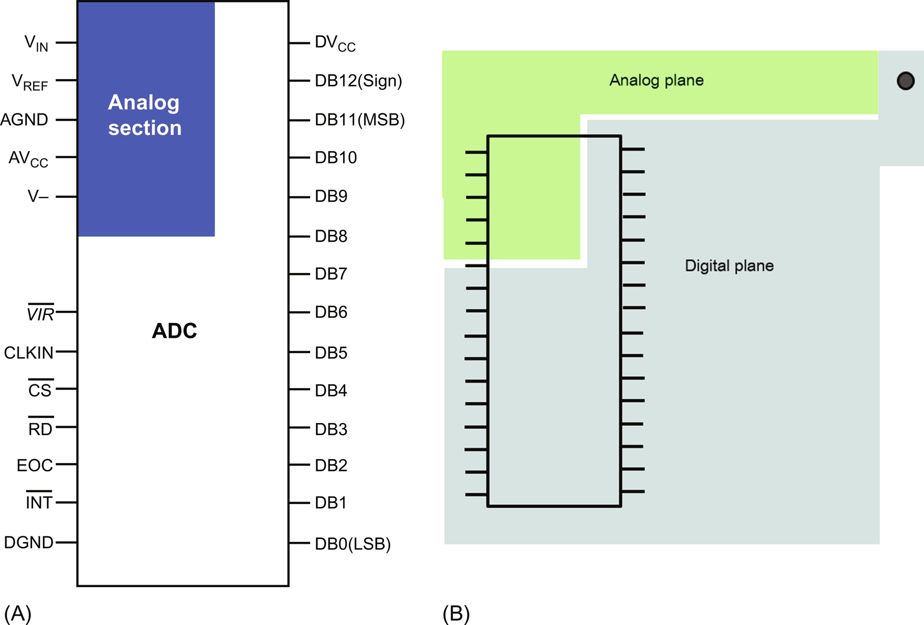
Notice how the analog section of the ADC is isolated from the rest of the digital section of the package with its own power and ground inputs. This likely carries over to the actual IC die. Separating the planes will ensure that current pulses into the ground plane do not affect the low noise requirements of the analog ground. Finally, the dot in the right diagram of Fig. 4.10 represents the connector pad of the PCB where the ground reference returns to the power supply.
One last hint with respect to ground planes. If your PC board vendor supports “thermal isolation pads,” then it is a good idea to use them. The thermal pads are indicated by the arrows in Fig. 4.11. Note how they look like a wheel with four spokes emanating from the through hole.
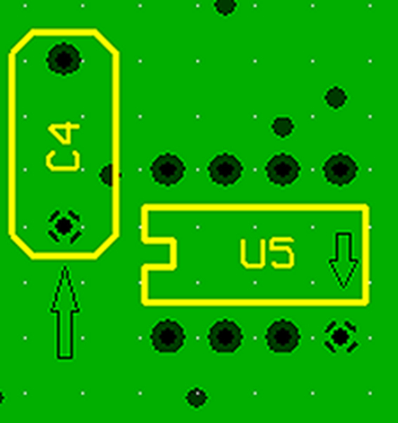
The purpose is to increase the thermal resistance of the pad, which, if the need arises, gives your soldering iron a fighting chance to unsolder the part from your PC board. Without the thermal pad, the copper layer is such a good thermal conductor that it will draw the heat away from the pad as fast as the soldering iron applies it.
A final note on grounding. I’ve included two application notes from Analog Devicesn on proper grounding techniques in the Additional Resources section at the end of the chapter. So, if you don’t want to buy a book, check out these application notes.
The last “best practice” I wish to suggest is the liberal use of power supply filter capacitors on your PCB. Students often ask me, “How many capacitors should I use?” I could launch into a long discourse, but I try to keep it simple. A good rule of thumb is one 10 μF electrolytic capacitor near the power input connector and a 0.1 μF ceramic capacitor near the Vcc input pin of each digital device.
One question I ask myself is whether a flaw in the design of a PCB is considered a bug? In other words, do I have a bug in my circuit even before I turn on the board? I would assert that is the case, so I offer this additional best practice, which is more of a guiding principle than an action. After designing many PCBs myself and helping countless students design and fabricate their own boards, I could make this observation. If a board is going to have a problem, there is a 75% probability that the problem will be mechanical, not electrical.
The experienced reader will probably laugh at this, but…. here’s my list of the most common board design errors that I’ve seen:
- • Wrong hole size
- • Part interference
- • Incorrect spacing for parts, particularly connectors
- • Improper pin numbering on connectors, especially if they are backloaded
- • Wrong pin size for connectors
- • Incorrect trace width
- • Failure to properly heat sink a part or provide proper cooling
- • Wrong part footprint
Wrapping up
This chapter was primarily about processes rather than “here’s how to find bug #7.” Yes, I did include some information about a few of my favorite best practices for designing printed circuit boards because so much of what a hardware designer does centers around the PCB that holds everything together. Again, this only scratches the surface of the topic. We could spend pages with discussions of glitch detection in FPGAso or similar, but that really isn’t my focus.
In later chapters, a number of these specific debugging issues will be covered (I hope adequately) when I discuss how to use the tools of the trade, so I hope that you, the reader, wasn’t misled by the content of this chapter versus its title.
Additional resources
- 1. www.debuggingrules.com: A web page devoted to debugging. Lots of good debugging war stories from engineering contributors.
- 2. Walt Kester, James Bryant, and Mike Byrne, Grounding Data Converters and Solving the Mystery of “AGND” and “DGND,” Tutorial Analog Devices, Inc., Tutorial MT-031, 2009, https://www.analog.com/media/en/training-seminars/tutorials/MT-031.pdf: Their list of references is worth the download by itself.
- 3. Hank Zumbahlen, Staying Well Grounded, Analog Dialogue, Volume 46, No. 6, June 2012, https://www.analog.com/en/analog-dialogue/articles/staying-well-grounded.html. According to the author,
Grounding is undoubtedly one of the most difficult subjects in system design. While the basic concepts are relatively simple, implementation is very involved. Unfortunately, there is no “cookbook” approach that will guarantee good results, and there are a few things that, if not done well, will probably cause headaches. - 4. http://www.interfacebus.com/Design_Termination.html#b.