
TESTING ANALOG-TO-DIGITAL CONVERTERS
8.1 Introduction
I used to say that testing an ADC was twice as difficult as testing a DAC. I was way off. It’s a lot harder than that. Much of the terminology for ADC testing is similar to the terminology for DAC testing, but the methodology is much different. An ADC produces a set of digital codes that correspond to the analog input level. Like a DAC, testing the DC performance of an ADC consists largely of verifying a consistent and linear response. In practice, however, there is very little similarity between testing a DAC and testing an ADC. Because the digital output for an ADC is valid for a range of input values, ADC testing is more complex than testing a DAC. The methods used for DAC testing generally cannot be re-arranged and applied to testing ADC devices.

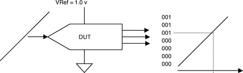
An analog-to-digital converter is non-deterministic from the output to the input. If a test condition specifies a certain voltage on the input of a perfect ADC, one can predict the digital output code. However, if only the digital output code is known, there is no way to predict the exact input voltage—only its range can be predicted. It is not possible to correctly test an ADC by treating the device like a reverse DAC. Simply applying DC voltages and checking if the ADC has the correct response is not an adequate test method. In practice, testing for ADC linearity requires measurement of the voltage threshold that causes a code output change.
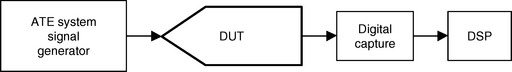
A typical test setup for testing the DC performance of an ADC device uses the test system signal source to generate an input voltage ramp via the ATE signal generator. The digital output codes generated by the ADC devices and the analog values corresponding to the output code transitions are then processed by the test system’s digital signal processor (DSP). Whereas DAC testing requires a high-precision measurement system to verify the analog output, ADC testing requires a high-precision signal generator to produce high-accuracy analog input levels.
8.2 ADC Overview
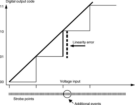
Let’s look at a simple, general-purpose ADC to get some ideas about testing requirements. An analog-to-digital converter will generate a single output code for a range of input levels. The next highest code is output when the input level exceeds a given threshold. Evaluating the linearity of an ADC device measures the voltage range between code thresholds. The first output code transition occurs when the device changes from all zeroes to the next code step. The all-zero code does not have a corresponding input range, only an upper threshold. Likewise, the maximum output code identifies the threshold transition point, but there is not a corresponding range of values that correlates to the maximum output code.
Linearity tests for an analog-to-digital converter concern the relative size of each voltage step that causes a change in the output code. In this tutorial, the voltage thresholds that cause a change in the output code are called Code Boundaries (CB). Linearity tests reference either the code boundary or the calculated center between code boundaries (code center). Because the test concerns voltage spans corresponding to code changes, the measurements are made between, but not including, the two endpoints.
Referring to the illustration of the 3-bit ADC transfer diagram in Fig. 8.2, there are clearly 8 possible output codes, or 2n, where n is the number of digital output bits. However, counting the step transitions across the x-axis indicates there are only 7 thresholds, or 2n − 1 code boundaries. When measuring the span between thresholds, a review of the transfer diagram shows there are only 6, or 2n − 2, equally spaced voltage spans corresponding to output code transitions.

Number of unique output code values = 2n.
Number of output steps = 2n − 1.
Number of input spans corresponding to an output code = 2n − 2.
In this chapter, we will use the nomenclature CB[n], where CB stands for the Code Boundary input voltage threshold, or Code Boundary, and n refers to the corresponding output code.
8.3 DC Test Overview
As with DACs, there are two general categories of DC tests for ADC devices. The first category evaluates the device minimum and maximum input code boundaries, referenced to an absolute specification. ADC offset measures the variation of the input level causing the first output code transition. ADC gain measures the overall input span from the first code boundary to the last code boundary.

The second category of DC tests evaluates the linearity by measuring the voltage range of the analog input steps that causes increments in the digital output code.

8.3.1 Offset Measurement
ADC offset is the difference between the ideal and actual analog input values that cause a transition from “zero code” digital output to the next code increment. The ideal “zero code” transition is calculated as a fraction of the reference voltage range, or Full-Scale Range (FSR). Offset is also known as the “Zero Code Error.”
Using our 1-volt, 3-bit converter as an example, the full-scale range would be 1 volt—that is, the reference voltage level. ADC devices are usually designed so that the first code transition should occur at one-half of the nominal step size, or LSB. The nominal or ideal step size is calculated by dividing the FSR by the number of steps (2n). The ideal first step Code Boundary (CB) for this device should therefore be 1/2 of .125 volts, or 62.5 mV.
If the measured first code transition threshold, CB[1], was measured at 72.5 mV, the difference between the ideal and actual indicates an offset error of 10 mV.
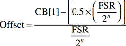
1. Calculate the ideal LSB voltage step as ![]() .
.
2. Calculate the offset error as = CB[1] − 1/2 of an Ideal LSB.
3. Divide the error by the Ideal LSB to derive the fractional LSB offset value.
Some devices are designed so the first threshold is equal to 1 LSB, in which case the offset is referenced to FSR/2n.

8.3.2 Gain Measurement
ADC gain is the difference between the ideal and actual span of analog input values corresponding to digital output codes. Because the offset shifts the entire transfer function, it is subtracted from the maximum code threshold level in order to normalize the reference. The total number of analog steps is 2n − 2, so the ideal span is equal to the full-scale range minus 2 ideal LSB steps. The full equation for the ideal span is FSR − (2 × LSB). The LSB is equal to FSR / 2n, so the ideal input span can be calculated as

Example
2. Measured span = Last code − First code
3. Gain Error = Measured span/Ideal span

Gain Test Example

1. Apply power to the device power pins.
2. Apply the voltage reference level to the VREF pin.
3. Adjust the input voltage until the output code changes from 110 to 111 to determine the CB(2n) value.
4. Subtract the first threshold value CB[1] from the last threshold value CB[111] to determine the DUT input span.
5. Compare the actual span with the ideal span as an error percentage.

8.4 Linearity Test Overview
Testing ADC device linearity evaluates the device in terms of the analog input steps corresponding to increments in the output digital code. The analog input steps correspond to the difference between two adjacent code boundary (CB) values. Ideally, each increment in the analog input value causing a change in the digital output code would be exactly the same range. In an actual device, the analog step size varies. The linearity of the transfer function is referenced to a calculated device step size (LSB).
The device LSB step is calculated by dividing the total span of the ADC by the number of corresponding analog input transition steps, or code transitions. The first code transition is not “all zeroes,” but actually the transition between all zeroes and the next increment. Therefore, the device LSB value is calculated referenced to the total number of codes, less the first code. Because the total number of codes transitions = 2n − 1, the total number of code spans is 2n − 2.
Differential Nonlinearity (DNL) is the difference between each analog increment step and the calculated LSB (device LSB) increment. DNL is also described as DLE, Differential Linearity Error.
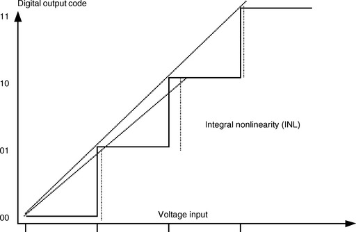
Integral Nonlinearity (INL) is the worst-case variation in any of the code boundaries with respect to an ideal straight line drawn through the endpoints. INL is also sometimes defined in comparison to a “best fit” straight line. INL is also described as ILE, Integral Linearity Error.

8.4.1 Differential Linearity
Example Device: 4-bit ADC with a 10.0 reference voltage
1. Calculate the actual device LSB code boundary width.
The transition from 0000 to 0001 occurs at 0.3 volts, which is CB[1].
The transition from 1110 to 1111 occurs at 9.9 volts, which is CB[15].
2. Driving the device with a ramp, the input level that causes the output digital code to change from 1001 to 1010 is measured at 6.1 volts.
3. For the next step in your test, the voltage input is increased until the device responds with a digital code of 1011. The input voltage causing the output code change is measured at 6.7 volts. The voltage increment for this step is therefore 600 mV (6.7 volts − 6.1 volts = 600 mV).
4. Calculate the value of the DNL for this bit, as a fraction of a device LSB.


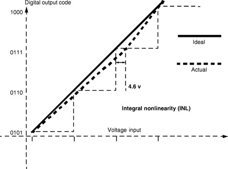
8.4.2 Integral Linearity
INL testing checks the overall “flatness” of the conversion range. An ideal ADC would have a straight line from the LSB value to the MSB value, with all of the intermediate codes in perfect alignment. An actual ADC will exhibit a curve from the ideal straight line, expressed as INL. From the previous example, we know that the voltage threshold for the first code transition is 0.3 volts. The voltage threshold for the last code transition is 9.9 volts. The linearity span is therefore 9.6 volts,which is divided by the remaining number of codes to give us the device LSB step-size of 665 mV. Remember that we are evaluating linearity based on the two endpoints derived from the offset and gain tests. When determining the “ideal straight line” of code boundaries, the calculations are referenced to the first code transition.
1. The ideal straight-line intersection is calculated by multiplying the device LSB by the code value −1, referenced to the first code transition threshold, CB[1].
For the example device, the device LSB was 665 mV, and the first code transition was 300 mV. For a perfectly linear device, we can predict that the threshold that generates the code of 0111 would be equal to the first code threshold, 300 mV, plus six additional steps of 665 mV each.
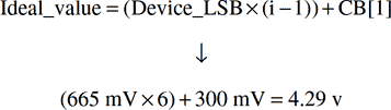
2. The actual input voltage level that causes the output code to change from 0110 to 0111 is measured at 4.6 volts.
3. The difference between the expected or ideal threshold value and the actual threshold value is a function of the device integral nonlinearity.

As with DACs, in practice the INL is derived from the collected DNL data. Performing an integral calculation on the DNL data set produces a “running average” that corresponds directly to the actual INL for each code. The maximum absolute value of the integral results is the same as the worst-case INL error.

8.5 Missing Codes
An ADC is said to have a missing code if the digital output codes have a gap; that is, the missing code is an output value that is never generated. A missing code can occur if there is no analog input value that can generate a specific code. If a bit combination has a positive DNL error of one-half of an LSB, and the subsequent bit combination has a negative DNL error one-half of an LSB, the overall effect will be a missing code. No missing codes can be inferred by testing for DNL errors of less than 1/2 LSB value.
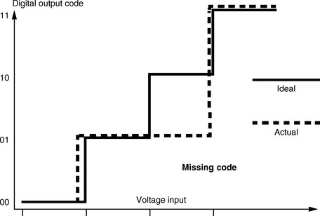
Non-monotonicity may occur with digital-to-analog converters, but could only theoretically occur with an ADC device. The error would indicate a negative code width. Under dynamic conditions, an ADC can appear to be non-monotonic because of the variations in the code boundary thresholds.
8.6 The Histogram Test Method
The power of digital signal processing can be applied to testing the DC linearity for ADC devices by use of a histogram. A histogram is a data structure that organizes data according to the number of occurrences of a value. The output of the histogram algorithm can be visualized as a bar chart displaying the number of events corresponding to a measured value. A histogram test typically drives the input of the analog-to-digital converter with a ramp that begins at the device negative full scale and extends to the positive full scale. The ramp is synchronized with the device clock so that a given number of conversions takes place for each consecutive voltage span corresponding to an output code.
Example
A 12-bit ADC DUT features a device LSB of 2.4 mV. The ATE system is programmed so that each time the DUT is clocked, the signal source increments the DUT input level by 150 μV. When the input level reaches 3.6 mV, the DUT begins to generate an output code of x02. The DUT continues to generate this output code until the input level reaches 6.0 mV, when it begins to generate an output code of x03.
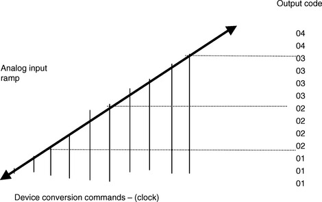
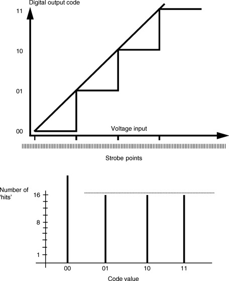
If the DUT features equally spaced analog input spans corresponding to a change in the output code, each code will be generated an equal number of times. Hey, it could happen, right? For example, if the input voltage level is increased by 1/16th of a device LSB for each conversion, then each code will be generated 16 times. Any variation in the code width will cause a variation in the number of occurrences of a given code, which corresponds directly to the DNL error. The number of events for the first and last codes per code is meaningless, because the first and last codes do not have a defined code width.
8.6.1 Events per Code
If the DUT has an input voltage span that is greater than or less than the device LSB, then the number of codes generated for that particular span will either be greater or lesser than expected. In this example, the output code transition from x01 to x10 did not occur until the input voltage level was above the expected threshold. As a result, the DUT continued to generate additional output code values of x01. There is a direct correlation between the number of events in the histogram, and the amount of DNL error for that bit.
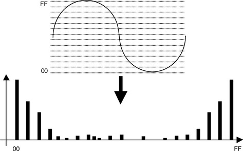
8.6.2 Weighted Sine Wave Histogram
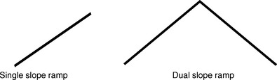
There are several different input waveforms that are commonly used for the histogram test method. Because the ADC code boundaries are subject to variation due to noise and hysteresis, a dual slope ramp, or triangle wave, often provides a more thorough test than a single full-scale ramp.
For devices intended for dynamic signal acquisition, a weighted sine wave histogram is sometimes the preferred approach. Instead of a ramp, the input signal is a multiple-cycle sine wave signal. The output data set is mathematically corrected, or weighted, to correct for the unequal histogram distribution of a sine wave. The unprocessed histogram of an ADC output sequence from a sine wave input will exhibit a “bathtub” distribution, along with a non-deterministic number of events for the lowest and highest code values. Correcting the sine wave histogram consists of removing the undefined endpoint values, and then scaling the histogram values to correct for the sine wave distribution.

The actual number of events per code from the histogram data set is divided by the ideal number of events for that code to produce a normalized histogram.
8.6.3 The Segmented Ramp
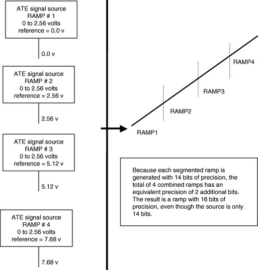
A hardware-based signal generation technique called the “segmented ramp” is sometimes used in conjunction with the histogram test method. In order to generate a precise ramp for high-resolution ADC devices, the signal source is programmed to generate a sequence of ramps, each referenced to a different DC base level. The analog input of the device is driven with a very precise ramp, which is actually composed of several smaller ramps in succession. Consider the following example, in Fig. 8.20, using a 14-bit signal source.
8.7 AC Test Overview
Testing the AC performance of an ADC requires applying an analog input signal and capturing the digital output of the ADC device. Like DC testing, a typical test setup for testing the AC performance of an ADC device uses the test system signal source to generate an AC signal, such as a sine wave. This sine wave data is applied to the test system waveform generator DAC to generate a sine wave.
It is particularly important when testing AC performance that the test system synchronize the analog signal input and the strobe of the digital output with the analog clock. The test will then process the signal data with the test system’s digital signal processor (DSP). As in AC testing for DAC devices, the speed of the digitizer is of greater concern than in DC testing. Test systems sometimes allow a selection of signal generators, allowing the test engineer to choose between a high-accuracy signal generator for DC tests, and a high-speed signal generator for AC tests.
The design of the test system signal generator may allow some flexibility as far as the sample rate and the number of samples per cycle. It is usually not necessary to use a power-of-two sample size for the signal generator sample set because the sample set will not be processed with a FFT. To get the best signal integrity from the ATE system signal generator, it is common practice to clock the signal generator at least 16 times the signal frequency. Any error from the signal generator can appear as error generated by the device under test.
8.7.1 Conversion Time
Testing conversion time consists of measuring the propagation delay from the beginning of a conversion to the expected digital output code. For some ADC architectures, such as flash converters, the conversion time can be tested in the same fashion as a propagation delay test for a digital device. Typically, the device is first conditioned by driving the analog input pin with a low voltage level, and then sequencing the device to generate a conversion. Once the output pins have been forced to a known state, the delay test consists of applying a full-scale input level and executing the device conversion sequence. The device digital output pins are strobed by the ATE system pin receivers within a specified time after the active edge of the device clock. If the device output data is correct, then the conversion executed properly within the specified conversion time.

Other converter designs, such as a successive approximation ADC, specify the conversion time in terms of the number of clock cycles required to generate the output code. In that case, conversion time is based on the specified clock count, multiplied by the clock period.
8.7.2 Harmonic Distortion Tests
The overall effects of errors across the entire range of digital codes can be expressed in terms of the ADC’s ability to accurately digitize a full-scale analog signal. Testing for harmonic distortion requires that the device be driven with a analog input sine wave, synchronized with the ADC conversion rate to make sure a maximum number of unique codes are tested. The input sample set ideally would have a number of samples equal to the total number of ADC code combinations. For example, testing a 12-bit ADC would theoretically use an input pattern of 4,096 unique samples. Because there are few samples at the sine wave zero crossing, a sample set of 5 times the number of DUT code combinations is the practical minimum.
The output of the ADC must be captured via the test system digital receive circuits, and analyzed with the test system DSP. Before performing signal analysis functions, the digital data set from the ADC is converted into floating-point form. A common convention is to map the largest code value (2n − 1) to a positive 1.0, and the smallest code value to 0.0. A 16-bit ADC, for example, would produce a set of output codes ranging from 0000 to FFFF. Converting this data to floating point would create a data set ranging from 0.0 to 1.0, with numeric increments of 15.258e − 6 for each LSB step. The scale need not correspond to analog levels because the dynamic measurements of distortion and noise are relative measurements.
An FFT converts the captured data into frequency domain information. The frequency domain data is analyzed by first measuring the amplitude of input signal frequency, which becomes the reference point for the harmonic content ratio. The amplitude for the frequencies that are integer multiples of the signal frequency are measured and summed, and then the results are calculated as a percentage, or as a dB ratio.

Interpreting the FFT Results for ADC Harmonic Distortion Tests
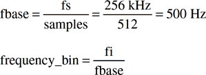
The test program applies a 20-kHz sine wave to the input of the ADC under test.
The device is clocked at 256 kHz, and generates a total of 512 samples.

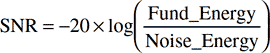
1. Find the harmonic energy as the algebraic sum of the harmonic signal energy.

2. Calculate the dB ratio of the signal to the distortion figure.
You can also colculate it as a percentage
Signal-to-Noise Tests
Like the DAC test sequence, the same frequency domain data set that is used to determine harmonic distortion can also be processed to derive the signal-to-noise ratio (SNR). By convention, the classic signal-to-noise measurement does not include the harmonic energy, only the non-harmonic error components. Because the SNR test is a statistical measurement, a valid number of noise components must be processed in order to generate a valid result. The capture rate (fs) and sample size must be chosen to produce a statistically valid number of data points, and a suitable bandwidth corresponding to the SNR specification.
The signal-to-noise ratio (SNR) of an analog-to-digital converter is tested by driving the DUT with a sine wave, with a known frequency and amplitude. The digital output of the device is captured and analyzed in the frequency domain by use of an FFT algorithm. Energy other than the DC and signal frequencies is a digitizing error known as noise. Testing for the SNR processes the result of the FFT to remove the energy components due to the DC value, the signal energy, and the harmonic energy. The ratio of the signal amplitude to the noise level is expressed in terms of decibels (dB).
Step One: Measure the energy value of the signal frequency (fundamental).
Step Two: Sum the noise energy
where s1, s2, s3, through sn are the frequency domain data points (frequency bins) that exclude the DC, fundamental, and harmonic signal components. A statistically valid number of noise samples, represented by the frequency bins values, is required.
8.7.3 The ENOBS Equation
ENOBS is one of those “insider” buzz words. You can impress your friends and neighbors by casually mentioning your estimate of the latest ADC performance in terms of ENOBs. Picture yourself by the water cooler saying, “You know, Joe, I’ve been looking at the spec for that new XYZ converter. It looked all right at first, but then I did a little digging. Did you know that the ENOBS is only around 10 bits?” You can bet that Joe did not know that, nor does he have a clue about what in the world an e-knob might be.
ENOBS is the effective number of bits, and offers another way of calculating the ratio of the signal energy to the noise energy. An 8-bit analog-to-digital converter (DAC), for example, has 256 unique digital codes. The effective resolution is 1 part in 256, or 1 LSB. Calculating the dB ratio for 1 part in 256,
The resolution error for an 8-bit ADC would therefore be −48.16 dB. Describing the noise ratio as an ENOB rearranges the equation to start with the dB ratio, and calculates the equivalent number of bits, normalized to a signal frequency at fs/2.
Testing for signal-to-noise ratio as the effective number of bits simply calculates the value from the SNR dB measurement. When using effective number of bits as the specification, a 10-bit DAC device with a noise measurement of 48 dB would be described as “Effective Number of Bits = 8.”
8.2
| Number of Bits | Number of Codes | Theoretical SNR (# bits × 6.02) |
| 10 | 1024 | −60.2 dB |
| 12 | 4096 | −72.2 dB |
| 14 | 16384 | −84.28 dB |
| 16 | 65536 | −96.32 dB |
8.7.4 Spurious Free Dynamic Range Tests
A conventional signal-to-noise test treats the noise component amplitudes as though they were a Gaussian distribution. That works well, most of the time. However, the method of deriving the noise figure as a square root sum-of-squares can sometimes hide a significant flaw. If the frequency domain data shows a big fat noise spike in the midst of an otherwise reasonable distribution, the error will be masked somewhat by the noise calculation.
Another way of testing for noise is to look for the peak spurious component, which is the largest spectral component excluding the input signal and DC. The value is expressed in dB relative to the magnitude value of a full-scale input signal. Specification of the Spurious Free Dynamic Range (SFDR) across a given frequency is perhaps the best single indicator of the device performance. Testing for SFDR requires the device be driven with a single tone with a full-scale amplitude. The maximum frequency component excluding the signal and DC component is measured, and the dB ratio is calculated relative to the fundamental signal strength.


8.7.5 Full-Power Bandwidth Tests
ADCs exhibit some amount of frequency roll-off at higher frequencies, as a function of the input sample and hold amplifier (SHA) and the device circuit capacitance. A full-power bandwidth test verifies that the roll-off meets or exceeds the specified limit. The full-power bandwidth of an ADC is the input frequency at which the amplitude of the reconstructed fundamental is reduced by 3 dB for a full-scale input. This test is often used for devices intended for undersampling applications, where the signal is actually higher than the device clock rate.
The test uses a low-frequency signal to generate the reference amplitude. A high-frequency signal, typically much higher than the device clock rate, is applied and sampled by the DUT ADC. By measuring the amplitude of the resulting alias, the test can determine the effective roll-off introduced by the device at the high-frequency test signal.
Example
1. The test program applies a 100-kHz sine wave reference signal at full-scale amplitude to the DUT, which is clocked at 1.0 MHz. The output data set is captured and processed with an FFT. The reference signal amplitude in the frequency domain has a value of 0.997.
2. The test program applies a signal at 3.2-MHz full-scale sine wave to the DUT, which is clocked at 1.0 MHz. The 3.2-MHz alias appears at the frequency bin for 200 kHz, with an amplitude of 0.812.
3. The full-scale bandwidth attenuation at 3.2 MHz is calculated as

8.7.6 Aperture Delay and Aperture Jitter
Aperture delay time is the amount of time from the active edge of the device sample clock until the device actually takes a sample. Unequal delay times internal to the device cause an effective skew between the analog signal and the start of the conversion process. In practice, the aperture delay is tested by applying a series of digital pulses to the input of the ADC device under test. The device sample clock is driven with a digital edge that is swept across the aperture range. The aperture delay time is determined by monitoring the device output response. The process is similar to testing setup and hold time for a digital device.
Aperture jitter is the sample-to-sample variation in the effective point in time when the sample actually occurs. Testing for aperture jitter is performed by repeated measurements of the aperture time. A number of measurements are taken to derive the standard deviation, and the amount of aperture jitter is calculated by statistical methods. Aperture jitter can be of interest because it is directly correlated to the signal-to-noise ratio and the repeatability of high-speed digitizing applications. The effective frequency of the aperture jitter error contributes to the overall noise factor as follows:


8.7.7 Aperture Delay Measurement
Aperture delay can be evaluated by measuring how long the input signal must be at a valid logic level before the active clock edge. During the test, the device is programmed so the output will change state if a valid input logic state is detected. The vectors are programmed to drive the data pin with the opposite data—which forces an “all-zero” output—before and after the test data. There are two timing sets used for measuring aperture delay. The first timing set describes a default set of edge placement values, which are well within the device performance range. The second timing set uses adjustable values, which are programmed in the successive approximation process.

1. When testing analog-to-digital converters, what is meant by a “code boundary”?
2. You apply 5.0 volts to the input of an ADC device, and measure the output code at 0100. Then you apply 5.2 volts and measure the output code at 0101. Is it correct to say that the LSB increment value is 0.2 volts? (Yes or No) Why?
3. You apply a 20-kHz sine wave to the input of the ADC under test.
The ADC under test is clocked at 256 kHz, and generates a total of 512 samples. The device output is captured and analyzed with a FFT.
What is the frequency of the third harmonic? _______
4. The output of the FFT from question 3 can be treated as a floating-point array with the set of array elements ranging from element [0] to (fs/2)/fbase. What is the location of the third harmonic element in the FFT array?