
MIXED SIGNAL TEST MEASUREMENTS AND PARAMETERS
So, you’re sitting in your office, pondering the spec sheet for a mixed signal device. The device does all kinds of cool stuff, but the trick is how to test the silly thing? About now, you might be thinking of a career change; or maybe joining the French Foreign Legion. Now what do you do? How can you determine if a mixed signal device is operating according to specifications? What are you going to measure? A large portion of mixed signal testing focuses on signal analysis. In this chapter, we will examine signal characteristics and their associated test and measurement techniques.
The procedure for signal analysis is simple: Apply the conditions, make some measurements, and perform some calculations. The signal analysis procedure usually produces a number, or set of numbers, that indicates some qualitative value corresponding to a signal characteristic. We’re looking for signal characteristic values, or the results of the analysis, to be within a certain range. Like hand-grenades and horseshoes, as long as the signal characteristic is close enough, we’ll say it passes the test.
If your background is in digital logic test, this may seem a little arbitrary. After all, the part is either good or bad; it either passes the test or it doesn’t. Right? But the truth is even some tests for logic devices, such as IDD current, are specified as “close enough” tests. If the IDD specification is 100 mA, that doesn’t mean that the device IDD must measure exactly 100.0 mA.1
What, or who, determines the specification for a signal parameter? (You’re not going to like this.) Signal characteristic specifications are not based on absolute truth. If your device has a total harmonic distortion level of 0.2%, is that good or bad? It depends. Mostly on what the marketing department says! Read this table and weep.
2.1
| Measured Value | Customer’s Expectation | Competitor’s Claim |
| 0.2% THD | 0.5% THD | 1.0% THD |
| 0.2% THD | 0.5% THD | 1.0% THD |
A distortion level of 0.2% is good, if the customer wants 0.5% and your competitor can’t deliver a part that is better than 1.0%. On the other hand, if the distortion measures 0.2%, the customer wants 0.1%, and your competitor delivers 0.1% devices at half the price, that’s a bad part. Very bad! On the bright side, even if the specifications are not based on absolute truth and cast in eternal stone forever, the methods for making the measurements are deterministic. That’s why they call it test engineering, after all. And yes, we’ll show you how to do a harmonic distortion test, a little later.
Example
You want to test an amplifier circuit for DC gain.
1. You apply the condition of 50 mV volt on the input.
2. You measure the output and read 0.4965 volts.
3. You calculate the gain, as the ratio of input voltage to output voltage.
4. You compare the results against limits, to see if the gain is close enough. The maximum specified gain is 10.5, while the minimum specified gain is 9.5.
![]()
2.1 Signal Analysis Categories
In general, signal analysis falls within one or more of three distinct categories—DC, time domain, and frequency domain. DC (direct current) signal analysis is used to determine the static or quiescent characteristics of the device, such as supply current or output pin voltage levels. Time domain, or AC, signal analysis applies to transient or dynamic signal characteristics. Typical time domain specifications include slew rate, pulse width, and settling time. The third category of signal analysis concerns measurements in frequency domain, such as noise and distortion. Mixed signal test employs a variety of methods to analyze the device response by measuring DC, time domain, and frequency domain characteristics.
2.2 Units of Measurement
Each signal analysis method has its own terminology and units of measurement. DC voltage measurements are expressed in volts or as a ratio, referenced to a specific test condition. The measurements may be either direct or inferred. Some voltage measurements are mathematically derived. Gain measurements, for example, are expressed as a ratio of output level to input level. The units may be in volts per volt, or in decibels. (We’ll talk more about decibels a little later.)
DC current measurements are expressed in amps or as a ratio, referenced to a specific test condition. Test system hardware usually measures current indirectly, based on the measured voltage drop across a known resistance.
Time domain measurements express a rate of change in voltage or current, and are referenced to seconds. Frequency can be indirectly measured in the time domain, and is expressed in Hertz (Hz). Evaluating signal characteristics such as pulse width or duty cycles measures the elapsed time between signal level thresholds. Other time domain characteristics, such as slew rate, are expressed as a ratio of voltage and time. Signal energy is a more sophisticated measurement, derived as the root mean square (RMS) of the signal amplitude across time and expressed as volts RMS.
Some signal characteristics are more easily quantified through analysis in the frequency domain. Noise, for example, can be detected in the time domain but not precisely measured. The frequency domain, however, allows straightforward evaluation of signal characteristics including noise and distortion. Frequency domain measurements are typically relative values, expressed as a decibel ratio or as a percentage. Noise is an amplitude measurement expressed either in volts or in power, or as a ratio of the signal amplitude to the noise figure. In the context of this book, noise is defined as a spurious AC signal, not harmonically related to the reference signal, or as a non-periodic error. We will define distortion as an AC signal error that repeats for each period of the reference signal, hence, a periodic error. Distortion is an amplitude measurement, expressed either in volts or in power, or as a ratio.
2.3 Decibel Calculations
A decibel is a method for describing a ratio. The original unit of measure was defined as the Bel after Alexander Graham Bell. (The Bel unit was originally defined as a measure of relative acoustic power as perceived by the human ear, and the ear has a logarithmic response.) One Bel is a huge value that no one ever actually uses, like a one-farad capacitor. In practice, one-tenth of a Bel is used to describe voltage and power ratios—a deci-bel. The term “dB” is an abbreviation for decibel, which in turn is simply a method for expressing a ratio.
There are many different ways to describe ratios. For example, the ratio of one nickel to a dollar can be described as 1:20, which indicates that there are 20 nickels to the dollar. Or, you could say that one nickel is equal to five percent (5%) of a dollar. It’s the same ratio, with different descriptions. The percentage references both values in the ratio to a scale of 100 so a ratio of 1:100 is the same as 1%.
Like a percentage, the decibel (dB) is a way of describing a ratio. Instead of referencing the ratio to a scale of 100, the dB system uses a logarithmic scale of log base 10. (When we see the expression log(x), it does not mean log times x, it means the log10 of x.) When used to describe a voltage ratio, a decibel ratio is defined as the following equation:
where v1 and v2 are the two voltage levels, or components, of the ratio.
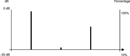
The expression derives the log of the ratio of v1 to v2, and we use a scale of 20 for measuring voltage, or 20 times log (x). There is a direct correlation between dB and percentage. Here’s the key: one percent is the same as 40 dB. Increasing the percentage ratio by a factor of 10 correlates to a 20 dB ratio increase.
Table 2.3
Correlating dB Levels with Percentages
| Percentage | dB |
| 1% | −40 dB |
| 0.1% | −60 dB |
| 0.01% | −80 dB |
| 0.001% | −100 dB |
2.3.1 Negative dB
Because a smaller ratio produces a larger dB value, the conventional representation of dB ratios are calculated “upside down.” The dB ratio of 1:1, or 100%, is equal to 0 dB. A ratio that is less than 100% logically correlates to a dB ratio that is less than 0 dB, or a negative number. A common method of referencing the calculation to 0 dB is to use a scalar of negative 20 (−20).
Where v1 is the reference level, and usually the larger of the two voltage levels.
Expressing the dB calculation as the ratio of the larger reference value to the smaller value has several advantages. First, the equation is mathematically consistent with the grammatical expression. The term “signal to noise ratio,” for example, implies that the ratio is derived from the signal amplitude divided by the noise amplitude. The second advantage concerns computational accuracy. In the case of extremely small numbers, the ratio can be corrupted by round-off error if the smaller value is divided by the larger value.
2.3.2 Power dB Ratio
The term power has some special considerations when calculating the dB ratio. Mixed signal tests are often concerned about the actual shape of the signal, and the term power is used to describe the effective energy, approximately correlating to the area under the curve. (It’s not exactly the same as area under the curve, but it’s close enough. After all, this is mixed signal we’re talking about here.)

Reviewing the simple equation for power, we find that relative power is a function of the square of the voltage.
Because log calculations are based on the law of squares, the effective squaring of the voltage level must be taken into account when calculating power ratios. To properly associate the power and voltage ratios, the dB calculation for power uses a scale of 10.

where p1 and p2 are the relative power levels.
You don’t believe me, do you? That’s cool, logs are squirrelly little buggers. Let’s look at it this way. The log of 5 is about 0.6987. Try it on your calculator, and see if you get the same answer. (If you don’t, you are probably using ln, the natural log, instead of log as in logarithm.) OK, now let’s see what happens with 5 squared. If you calculate the log of 25, you get 1.39794. Now, watch carefully as we pull the rabbit out of the hat: Voila! 1.39794 is equal to twice the value of 0.6997.
The same thing is going on with power and voltage. If you’ve got 5 volts into 1 ohm, then the power is equal to 25 watts.

2.4 Signal Analysis and Test Methods
Signal analysis is the last step in the generalized test process of source, capture, and analysis. The first part of the test process establishes the correct conditions, or stimuli. Signal information from the device under test is captured, and then evaluated according to specifications. We will examine the three aspects of signal analysis—DC, time domain, and frequency domain—in the context of a test sequence for mixed signal device. The example device is a programmable gain amplifier (PGA) with eight digitally programmed gain settings.


2.4.1 The Test Plan
The test engineer creates a test plan document based on the device specification document or “spec sheet.” The device specification document describes the operation and electrical characteristics of the device. In addition to the specification document, the test engineer also takes into consideration his or her own experience, knowledge of the ATE system capabilities, and prescribed conventions.
Designing the Test List
The order of tests is arranged in a sequence that will most quickly identify possible defects. The most basic tests are usually performed first, with the view that if the part fails the basic tests, then it is not necessary to test it any further. The order of tests must also take into consideration how a failure is identified and recorded in the data log.
For example, suppose the device under test has a defect in the power supply pin connection—the bond wire was not attached from the package pin to the die pad. If the first test is an output amplitude test, the device will fail and the failure will be recorded as a functional failure. Describing this device as a functional failure does not accurately identify the actual problem.
Some conventions have developed that help to organize the test flow to provide the most accurate information.
1. Is the tester connected to the device? (More on this later!)
2. Is the power supply current within spec? (IDD) (If not, there’s no point in going further)
3. Is the input pin current within spec? (IIH, IIL) (If the inputs do not work, nothing else will work)
4. If the connections, the power supply, and the inputs are within specification, then the test flow can evaluate the device functionality.
The functional tests, in turn, also follow a logical order to properly identify the failure mechanism while also minimizing test time.
2.4.2 The Test List
Beginning with the specifications, the test engineer develops the test plan and test list.
Example Test List
Continuity: The continuity tests verify proper connection of the DUT. If the DUT is not present or not properly connected to the test system, no tests can be performed.
Supply Current: The supply current tests verify that the amount of current on the device power supplies is within specification. This test also is a way of checking for certain types of gross process errors. If there is a gross process error that causes a large supply current, it is more efficient to identify the flaw early in the test process.
Leakage Current: The leakage tests measure the amount of current flowing on the device input pins. Excessive current can cause unreliable operation. Measuring leakage current is another check for gross process errors.
Offset Voltage: The offset voltage test for analog amplifiers measures any required adjustment on the amplifier input to force the amplifier output to zero volts. The offset measurement combined with the maximum output level test is a quick verification of device functionality.
Maximum Analog Output: Leakage and offset tests verify proper operation of the device input circuits. The compliance of the output stage is verified by measuring the maximum output voltage level under a specified current load.
Over Level Function: One of the conditions for testing the over level function is identical to the condition for the maximum analog output test, so for the sake of efficiency the two tests are grouped together. If the amplifier output is at the maximum level, the OV_LVL pin should be active.
Gain Error: The gain test evaluates the overall span of the amplifier output. Once the minimum and maximum range of the amplifier is tested via the offset and maximum output level tests, the actual output span can be calculated and compared with the ideal.
Linearity Error: If the device is perfectly linear, each gain setting should cause the amplifier output level to increment in equally spaced steps. To verify acceptable linearity, the amplifier output is measured under various combinations of input levels and gain settings. The response of the device is compared with a calculated ideal, and variations from the ideal are identified as linearity errors. Linearity tests are more time-consuming than other tests, and therefore placed at the end of the test list. Only devices that have passed all other tests are candidates for additional test time investment.
2.5 DC Test Outline
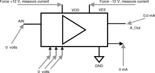
The purpose of continuity tests is to verify that the test system is properly connected to the Device Under Test (DUT). Continuity tests verify that all DUT signal pins are connected to the tester channels. Continuity tests also verify that the pins of the DUT are properly connected to the internal device circuitry. The measurement results can reveal significant information on the DUT itself, in addition to verifying the DUT-to-tester connection. The test measurements may be used in a database for controlling and monitoring the manufacturing process. The continuity test is a powerful and simple test and yet it is often the most misunderstood. Continuity tests do not check a specified device parameter, and are not specified in the data sheet.
Continuity tests verify the presence of the internal diodes for each input and output pin. The internal diodes are tested by forcing a current and measuring the voltage drop. Because there are usually two diodes per signal pin, at least two tests are performed. By forcing a forward current through the upper or lower diodes, one expects to measure a diode drop, typically between 600 mV and 700 mV. Because the return path of the forced current is through VDD or VSS, VDD must be grounded.

The VDD diode, or upper diode, connection for each pin is tested by forcing a positive current to activate the VDD diode, given that the device VDD pin is set to 0 volts. The current force resource is typically set to clamp at 1.0 volt. If the measured voltage drop across the diode is too high (typically greater than 0.8 volts), the diode connection is an open circuit. If the measured voltage drop across the diode is too low (typically less than 0.5 volts), the diode connection is shorted to VDD. The results are why continuity tests are sometimes called “opens and shorts” tests.
The VSS (GROUND) diode connection for each pin is tested by forcing a negative current to activate the VSS diode. The current force resource is typically set to clamp at −1.0 volt. If the measured voltage drop across the diode is too high (more negative than −0.8 volts), the diode connection is an open circuit. If the measured voltage drop across the diode is too low (less negative than −0.5 volts), the diode connection is shorted to VSS.

If VDD or VSS pins are open, or if the tested pin is shorted to VDD/VSS, the continuity test fails. This test does not detect if the pin under test is shorted to another pin. One method to detect pin-to-pin shorts is to perform the continuity test on each pin serially (one pin at a time), and to force all pins, except the pin under test, to 0.0 volts. (Forcing all pins to 0.0 volts is easily accomplished by using the test system functional drivers.) If the pin under test is shorted to another pin, the test will measure 0.0 volts instead of a diode drop voltage. The 0.0-volt measurement will cause the test to fail.
2.5.2 Supply Current Tests
The supply current tests verify that the DUT supply current is not excessive. Although it is usually not specified, it is sometimes good practice to check for a minimum supply current. There are two methods for testing the device supply current.
The first method is called static testing, because the device is not active. The second method is called dynamic testing, because the device is active while the current is being measured. Because the instruments for measuring DC values are slow in comparison to typical device execution speeds, dynamic testing usually makes use of a functional test loop. The device runs the same sequence repeatedly until the DC measurement is complete.
The IDD current can be measured once the device is in the specified condition. It is usually good practice to plan for a settling time delay after the conditions are programmed and before making the measurement. There are some factors that may prevent the device from reaching the specified condition immediately, particularly the load board bypass capacitors and the settling time of the ATE system instruments.
2.5.3 Input Pin Current Tests (Leakage)
Input pin current tests verify that the device inputs do not require excessive drive current. Leakage tests are performed with the power supply pins set to the nominal operating level. IIL (input current at logic low) is tested by applying a logic state using the specified VIL level, and measuring the current flow into the pin.
IIH (input current at logic high) is tested by applying a logic state using the specified VIH level, and measuring the current flow into the pin.
To test for pin-to-pin leakage, it is common practice to pre-set the voltage level of all input pins to the opposite extreme of the pin under test. If the IIL test requires an input level of 0 volts, only the pin under test would be forced to 0 volts. The other input pins would be forced to a logic high level.


2.5.4 Offset Voltage
Offset voltage measures the voltage correction required on the amplifier input to force the amplifier output to zero volts. Because of process variations and imbalances in the internal circuitry, a zero volt level on the amplifier input does not always cause the amplifier output to generate a zero voltage level. In that case, the input must be adjusted to achieve a zero voltage output level. The amount of required adjustment or correction is the input offset. The device specification defines an acceptable range of offset values.
For most tests, the general approach is to apply a known input condition, and verify the output response. Offset tests reverse this approach. The objective is to determine the input level that corresponds to a known level on the output.

In this example offset test circuit, the ATE system DSP unit controls the device input level via the Programmable Source instrument. By a successive approximation process, the DSP evaluates the DUT output level acquired by the measurement system, and adjusts the input level until the DUT output is zero volts. The input level required to force the DUT output to zero volts is evaluated as the input offset voltage.
2.5.5 Output Compliance Tests
Conductive parameter tests verify the drive capability of the amplifier output pin. The conductive parameter tests measure the output voltage level with a specified current load. Output current tests measure the current capacity on the output pin of the device when the output level is at the specified condition. Output voltage tests measure the voltage drive level on the output pin of the device for a specified logic state. The output voltage drive level is tested by verifying that the amplifier output can generate an acceptable voltage level with a specified current load.
Conductive tests verify that the voltage and current drive capability of the output pin under test is adequate. The device must be able to generate output levels with enough current to drive the circuit load. In the end-use application, a device that cannot supply sufficient current on the amplifier output pins will cause unreliable operation. The compliance of the DUT output circuitry is verified by measuring the maximum output voltage level under a specified current load. If the output is measured only under low current conditions, excessive “on resistance” of the output stage could remain undetected.
The device output levels are specified in conjunction with a current load. The Current Output Low (IOL) specification describes how much current the output must supply when generating a negative voltage level. IOL is referred to as device sink current, because current flows into the device toward ground. A negative output level “pulls down,” so the tester resource must source current. The Current Output High (IOH) specification describes how much current the output must supply when driving a logic high. IOH is referred to as device source current, because current flows from the device toward ground. A positive output level “pulls up” with a positive current flow, so the tester resource must sink current.
The analog output of the DUT amplifier is rated at positive 10 volts with a 5 mA load, and negative 10 volts with a −5 mA load. The absolute maximum output level is +/−10.5 volts. To test the maximum output level, the device is powered with +/−12 volts, with all digital inputs set to 0 volts. The analog input is driven with 10.5 volts, and the analog output level is measured and evaluated against limits. The process is repeated using a −10.5 volt input to test the negative voltage output compliance.
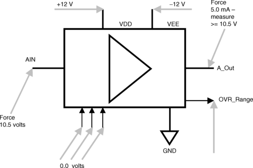
2.5.6 Over-Range Function
The device over-range function provides an indication of an over-range condition on the amplifier output via a logic level on the OVR_Range digital output pin. This pin goes to a logic high when the analog output level exceeds +/−10 volts, with a 100 mV margin. The maximum analog output test procedure has already verified that the OVR_Range pin goes to a logic high (>3.2 volts with a −5 mA load).
Another set of tests must verify that the over-range function produces a logic low when the analog output level is less than the maximum. The current load for the OVR_Range pin is set to +5 mA, and the logic threshold (VOL) is set to 0.2 volts. The analog input is set to +9.9 volts, and the OVR_Range pin is checked for a logic low. The analog input is set to −9.9 volts, and the OVR_Range pin is again checked for a logic low.

2.5.7 Gain Error Tests
The gain test evaluates the overall span of the amplifier output. Once the minimum and maximum range of the amplifier is tested via the offset and maximum output level tests, the actual output span can be calculated and compared with the ideal. Gain error is a measure of the overall device range, compared to an ideal range.


The difference between the actual and ideal is calculated as a percentage, as follows:
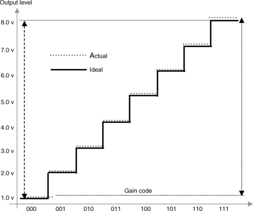
2.5.8 Linearity Error Tests
Linearity error measures each gain step by changing the gain setting with a constant input voltage level. The incremental steps of the output are compared to a calculated linear “straight line.” Based on the two measured end points derived from the gain test, we can calculate the overall span for this device as 7.1 volts. Between the first and last level, there are 7 gain steps, so each gain step should increase the voltage output by 1.014 volts per step.
With an input voltage level of 1.00 volts and a gain setting of 1, the DUT generated an output level of 1.05 volts. Changing the gain setting should produce equally spaced increments of 1.014 volts each, with a final value of 8.15 volts. Comparing the output level for each gain setting with the calculated level tests the device linearity.


2.6 Time Domain Tests
Like the DC tests, time domain tests begin with the device specification. In the example case of a programmable gain amplifier, several dynamic characteristics are specified. The purpose of the dynamic specifications and tests is to ensure adequate device signal performance.
2.6.1 Slew Rate and Settling Time
The time domain specifications for the example device include slew rate and settling time. Slew rate describes the slope of a voltage change across time. The DUT is driven with a fast edge pulse, and the output is captured and analyzed. The slew rate is found as the slope of the transition between the rated output extremes. Sometimes the positive and negative swings will have different slew rates, in which case both positive and negative slew rates are tested.
Settling time measures the time elapsed from the application of a step input to when the amplifier output has settled to within a specified error band of the final value. Settling time includes the time needed for the DUT to slew from the initial value, recover from any overload, and settle to within a specified range.
Because the test procedures for slew rate and settling time use an identical set of test conditions, the two tests can be efficiently grouped together. In both cases, the device is powered up and programmed for a specific gain value. A square wave signal is applied to the amplifier input, and the amplifier output signal is captured and analyzed.

The captured signal from the device output is analyzed by the DSP unit. The DSP calculates the slew rate by measuring the period between two thresholds of the signal slope. Settling time is calculated from the captured signal information as the time between the beginning of the slope, and when the output state is within the specified range of the new output level.

2.6.2 Frequency Response Tests
Mixed signal devices may be specified to operate over a range of signal frequencies. A frequency response test measures how the device responds to different signal frequencies across a specified range. Frequency response can be measured in either time domain or frequency domain.
Test Procedure: The device is powered up and programmed for a specific gain value. Three separate measurements are performed, using three different input signal frequencies. The first measurement applies a 1000 Hz sine wave, with a 1.0 volt peak-to-peak amplitude. The output signal amplitude is measured at 1.05 volts. The second measurement applies a 5000 Hz sine wave, also at 1.0 volts peak-to-peak. With a 5000 Hz input signal, the output signal amplitude is measured at 0.95 volts. The third measurement applies a 10 kHz signal at 1.0 volts peak-to-peak amplitude, which results in an output amplitude of 0.73 volts.


2.7 Frequency Domain Tests
A faster way of measuring frequency response is to use one input signal that is composed of several frequencies, a signal known as multi-tone.
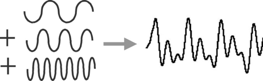
2.7.1 Multi-Tone Signal
By applying a multi-tone signal, the device response to each frequency component can be evaluated by processing the device output in the frequency domain. Multi-tone testing uses a DSP process that deconstructs the device output signal into a data set of amplitude values at discrete frequencies. The result of the DSP algorithm, known as the Fourier Transform, allows relative measurements of distinct signal frequency components. Using the DSP to generate and process signal data as discrete frequencies is called frequency domain analysis.

2.7.2 Noise and Distortion
The DUT introduces errors into the signal, which can be analyzed as distortion and noise. The specifications for the example device describe the output signal purity as a maximum allowable error ratio, referenced to the primary signal.
| Harmonic Distortion | <5% at 1000 Hz at 1 volt |
| Signal to Noise | −60 dB with 1000 Hz reference at 1 volt |
Distortion is an error in the signal shape, and occurs for each signal cycle. Distortion errors are therefore multiples of the fundamental frequency, and are called harmonics. Noise is random error that is not related to the shape or period of the original signal. Noise is usually defined as spurious signal energy in the output signal of the device, which occurs at non-harmonic intervals of the original signal frequency.
The stimulus data for both distortion tests and noise tests is a single-tone sine wave, known as the fundamental frequency. Assuming that the input signal is relatively pure, any difference between the input signal and the output signal is error introduced by the device.

2.7.3 Testing for Distortion and Noise
The test process for distortion and noise testing applies a pure sine wave to the DUT. The output of the DUT is captured and processed with a Fourier Transform. The Fourier Transform is a mathematical process that organizes the signal information according to variations of amplitude across frequency. (More on this later!)
By evaluating the frequency domain data, the amplitude of the original signal frequency can be compared with the amplitude of the signal distortion, which occurs at integer multiples of the original frequency. Signal information that is not the original signal frequency and not an integer multiple of the original signal frequency is identified as noise.

