TEST CIRCUIT DESIGN CONSIDERATIONS
9.1 Printed Circuit Board Physics
Everybody can draw a schematic, and if you’ve had enough practice, it might even make sense. But getting a circuit to actually work, that’s the hard part. So, what is the problem? The problem is that a physical circuit is much more complex than a theoretical circuit. The success of a mixed signal application depends on the proper design of the application software and test circuit hardware. Design of the mixed signal hardware must take into consideration requirements beyond connecting the device to the tester resources.
As an example, a 16-bit ADC with a 10-volt full-scale input has a 1 LSB value of 153 μV. To achieve an error margin of 1/2 of an LSB, the load board circuitry can generate no more than 76 μV. That’s not much, bubba.
Load board effects that must be considered include
The problem is that a physical circuit is more complex than a theoretical circuit. This additional complexity of a physical circuit is expressed by the following laws of Mixed Signal Test applications: Ohm, Kirchoff, Faraday, Lenz, and Murphy.
The voltage drop across a resistor is equal to the current flow multiplied by the impedance, E = I × R. Look, I know that you already know Ohm’s law. But it bears repeating here because a little tiny amount of resistance, say, in a wire or in a socket interconnect, can introduce some serious problems.
The current flowing into any point is equal to the current flowing out of the same point. The sum of voltage drops in a circuit is equal to the sum of the voltage rise. Which is to say, you don’t get something for nothing.
Two adjacent conductors separated by a dielectric are a capacitor. This is true even if two adjacent conductors are two traces on the circuit board and the dielectric is the circuit board fiberglass.
Current flowing through a conductor creates a magnetic field. A magnetic field that passes through a conductor creates current flow. Inductive coupling between adjacent components on a circuit board can create some interesting effects, such as noise and oscillation. The most important law pertaining to Mixed Signal Test Applications, however, is Murphy’s Law.
In any set of circumstances, the worst thing that can happen, will. Any effect you think can be disregarded, can’t. Nature always sides with the hidden flaw.
9.1.1 Trace Resistance
A resistor is not only found in those black, gray, brown, or multi-colored little cylinders with wire ends. Wires, PC traces, and socket connectors are also resistors. A common choice for PC trace width for digital device load boards is 0.25 mm. The resistance of standard PCB copper is 0.45 milli-ohms per square millimeter, so a “standard” digital PCB trace has a resistance of 18 milli-ohms per centimeter.
What would be the effect of a 5-cm length trace (standard 0.25-mm width) between the test system’s analog source, and 16-bit A/D with an input impedance of 5 K?
The trace resistance acts like a divider resistor in series with the device input impedance, creating a voltage drop equal to 1 part in 55,000 (1:55 k), or 0.018%. In comparison, an analog-level increment of 1 LSB for a 16-bit A/D converter is 0.0015% of full scale. There is more error introduced by the trace resistance than is generated by the device.

Every doubling of the trace width reduces the resistance by half. Use wide traces whenever possible. To correct for the voltage drop, use Kelvin connections from the tester resources wherever possible. In applications where the trace resistance is critical, measure the resistance with a milli-ohmmeter, and compensate for the error in software.
9.1.2 Force and Sense Connections
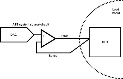
The ATE system signal source hardware may include force and sense connections, which allow the source to correct for any voltage drop due to trace resistance. The output of the source circuit behaves like an op-amp configured as a force compliance servo loop. The op-amp will drive its output to be whatever is required to balance the two input levels. To force compliance with a voltage drop in the force line, the op-amp output will generate a voltage offset to correct for the difference between the reference and the sense line.
Usually, the best results are achieved by connecting the force and sense lines together as close to the device pin as possible. This allows the Kelvin circuit to compensate for any voltage drop caused by trace resistance on the load board.
9.1.3 Skin Effect
Inductance at high frequencies has the effect of causing current to flow only on the surface of the conductor, which increases the effective resistance. The amount of resistance increases by the square root of the frequency. At the typical printed circuit trace thickness of 0.038 mm, the skin resistance of a 0.25 trace per centimeter can be calculated as
Example

High-frequency current flows only in surface layers, and wide traces provide a large surface area. Particularly for high-current transients such as those found in a ground return connection, a large surface area reduces the skin effect impedance.

9.1.4 Circuit Board Inductance and Capacitance
All conductors are inductive. The inductance of a standard 0.25-mm PCB trace is about 10 nH per centimeter. The formula for inductive reactance is
Therefore, at 10 MHz, a PC board trace length of one centimeter has a reactance of 0.62 ohms. For a 50-ohm system this can create a greater than 1% error. Inductance is directly related to the length and surface area of the conductor. Short wide traces have the lowest inductance. Long narrow traces have high inductance.
An inductor in series or in parallel with a capacitor forms a resonant, or “tuned,” circuit. A resonant circuit can cause oscillations. If the circuit is behaving erratically, but the problem seems to disappear when you apply a scope probe to the circuit node, chances are you have a tuned circuit. What happens is the capacitance of the scope probe retunes the resonance to a less troublesome frequency. Spurious oscillations of this sort can usually be corrected by adding surface-layer ground plane, or re-orienting the trace layout in the specific circuit section.
Circuit Board Capacitance
Capacitance can exist between two adjacent conductors that are separated by an insulator. If there is a change in voltage on one conductor, there will be a change in charge on the other. General-purpose PCB material has a capacitance of about 3.0 pF per square centimeter for conductors on opposite sides of the board. A grounded conductor between the two “plates” of a capacitor functions as a Faraday shield. The shield must be connected to block the coupled noise and allow the noise current to return to ground without flowing through a sensitive section of the circuit.

9.2 Resistor Physics
Discrete component resistors include some amount of capacitance and inductance, as well as an effective noise generator based on the junction of two dissimilar materials.

• The capacitance (C) of a resistor is typically around 5 pF.
• The inductance (L) is typically around 1 or 2 uH.
• The thermoelectric effect (n) of the ni-chrome to copper/nickel junction of a wirewound resistor is 42 μV/C.
Thermal noise, also known as Johnson noise, is found by
where
Reducing the resistance, the bandwidth, or the temperature will reduce thermal noise.
9.3 Capacitor Physics
A capacitor as it behaves in a mixed signal application is actually a complex parallel network of capacitance, resistance, and inductance.

The leakage resistance (RL) illustrates the leakage current path. Electrolytic capacitors have a current leakage of about 20 nA per uF. Tantalum capacitors have a much better leakage current of around 5 na per uF. Besides, if you wire an electrolytic capacitor in backwards, when it explodes, it makes a big mess and bad smell. You end up with confetti and oil all over, along with the smell of burnt squash. On the other hand, if you wire a tantalum capacitor backwards, it will emit a column of flame and smoke, which is really quite dramatic, but the smell tends to dissipate much more quickly.
The series resistance (RS) illustrates the power dissipation that occurs in capacitors. This can be a concern with RF applications, and power supply decoupling caps that have a high ripple current.
The series inductance (L) of a capacitor is created by the physical structure. In general, electrolytic, paper, and plastic film capacitors may tend to behave more like inductors at frequencies above 1 MHz. Monolithic ceramic caps have very low series inductance, and are usually a good choice for high-frequency applications.
9.4 Circuit Board Insulators and Guard Rings
The insulator resistance on a F4 fiberglass PCB varies from one section of the board to another. The resistance laterally (such as between two plated feed-throughs) is usually much lower than the resistance between two surface traces. A clean PC board will usually have an insulation resistance of between 10 and 100 Mega Ohms per cm. Besides worrying about ground currents and supply currents, sometimes we have to worry about the current that is sloshing around on the surface of the circuit board fiberglass. In applications that involve very high impedance and very low currents, the sensitive circuit section can be isolated from the effects of board leakage by a guard ring. A guard ring is a circular trace around the sensitive circuit point, which is driven to the same voltage level. A guard ring on both sides of the board will create the condition of no voltage drop across the protected circuit area, which in turn creates the condition of no current flow from leakage resistance.

9.5 Test Circuit Ground
In a physical circuit, GROUND is not a schematic symbol. GROUND is a current return path. Other than the lie about how being an engineering major would make it easy to meet attractive people of the opposite sex, this is probably the biggest lie we were told in engineering school.

The ground symbol has little or nothing to do with the actual flow of ground current. A friend of mine likes to say, “Ground is like the ocean.” Really, he actually says that. If there is anything like an ocean in an accurate analog of ground, it would be “Ground is like a two-lane dirt road to the ocean on a summer afternoon.” As in, lots of traffic, backups, and collisions.
Kirchchoff’s law tells us that current has to come from somewhere, and has to go somewhere. Every variation in current from the power supply and device I/O pins is reflected in the device ground as a current return path. Because a mixed signal test circuit ground is implemented with wire and circuit board copper, all of the physical effects of an actual conductor also apply to ground—particularly resistance and inductance. Ground might theoretically be ZERO volts, but it is not ZERO current.
Transient ground current can be much greater than the specified average IDD current. A 16-bit ADC driving 100 pF on each output pin with a 5-volt 5-ns swing can generate 1.6 amps of transient current.

All of the transient current will be present in the ground return path. Any impedance in the ground return path will create a voltage drop that is sometimes called “ground bounce.”
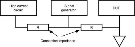
9.5.1 Ground Loops and Shared Ground Current
A ground loop problem can occur when a circuit has more than one return to ground, and that ground return path is shared with another circuit. The resistors illustrate the impedance of the ground connection path.
In Fig. 9.10, both the AC signal generator and the 10-volt DC source have a path to ground with some finite impedance, resulting in a voltage drop. The DUT ground is connected, via a finite impedance, to both the “AC Ground” and the “DC Ground.” Both the AC and DC ground currents create an offset voltage at the DUT ground point. There are different ways to represent a ground loop. In essence, a ground loop occurs when an external circuit shares the same ground return path as the signal circuit. A serial (or “daisy-chained”) ground can cause the same types of problems as a ground loop.

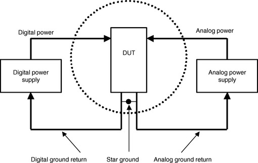
9.5.2 Star Ground
One approach for avoiding shared ground paths is to design the ground scheme so that each circuit section has a separate path to ground. This produces a single point in the circuit that serves as the ground, to which all circuit voltages are referenced. That single point is known as the “star” ground.

The star ground is an important concept that is often combined with other techniques to achieve an optimal grounding design. One of the problems that must be addressed is that the power supplies have their own ground paths. The supply current that flows through the existing ground paths may be of a high value, or just noisy. Kirchoff’s Law applies to AC currents as well as DC, and it certainly applies to ground current. Any transient current flow on the supply, such as may be caused by digital circuit activity, is mirrored in the ground current.
Digital circuitry is noisy, and is designed to tolerate noise. Analog circuitry is quiet, and cannot tolerate noise. Circuit noise in the form of current transients carried by power supplies and the ground returns can create errors in analog circuits. In mixed signal applications, it is usually best to dedicate separate power supplies to the digital and the analog circuit sections. Each supply should have a dedicated ground return path.

9.5.3 The Ground Plane
Because the lowest impedance path is achieved with the widest possible trace, a trace that covers a large portion of the circuit board is called a “plane.” The ground plane is simply a very wide trace that allows a low impedance current return path. Analog and digital grounds must be connected at one point, which serves as the star ground reference.
The test circuit ground planes serve several purposes. The primary function of a ground plane is to provide a low impedance current return path. The ground plane can also function as a Faraday shield between signal traces, either between circuit board layers or between adjacent traces on the same board.

The inductive field generated around components that are mounted on the surface of the circuit board can couple into adjacent components. A ground plane on the surface of the circuit board decouples the inductive fields.

9.5.4 Split Grounds
Many mixed signal devices have separate supplies and separate ground pins for the analog and digital grounds. The data sheets on these devices usually advise to connect these pins together at the device package. It is usually best to heed this advice. The problem the device manufacturer is trying to address concerns the limitation of the device package technology. The voltage drop in the bond wires is too large to allow the connection to be made internally.
The labels “analog ground” and “digital ground” on the device pins refer to the sections of the device to which the pins are connected. The labels of “analog ground” and “digital ground” are not intended to communicate the ATE system ground preference. (You may find it surprising to learn that design engineers do not stay awake late at night trying to figure out how to make life easy for the test engineer.) Optimally, it is usually best to conform to the DUT manufacturer’s advice and tie the device digital and analog grounds together at the DUT, making that point the star ground. If that is not feasible, all of the DUT grounds should be tied to the analog ground.

9.6 Power Distribution
The power connections to the device under test must also provide a low impedance path for the supply current. The same principles that apply to ground current paths also apply to power supply current paths. As with the ground connections, a very wide trace area or plane provides the lowest resistance and inductance. Circuit board planes that supply current are known as power planes. The transient power required by the DUT is much higher than the average DC current. Even though the VOH/IOH and VOL/IOL specifications may indicate a higher level of equivalent impedance, the transient impedance is much lower, and transient current for digital output pins is much higher. Reviewing the previous example, a 16-bit ADC driving 100 pF on each output pin with a 5-volt 5-ns swing can generate 1.6 amps of transient current.
9.6.1 Power Supply Decoupling
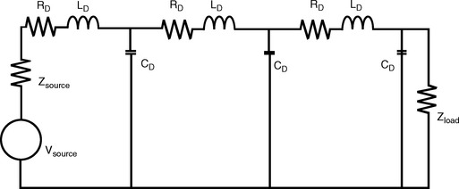
Most ATE systems are designed with the power supplies located in the mainframe connected to the test head with a long cable. In order to supply large amounts of current in a short amount of time, the power supply must have a local current reservoir as close to the device as possible—the bypass capacitors.
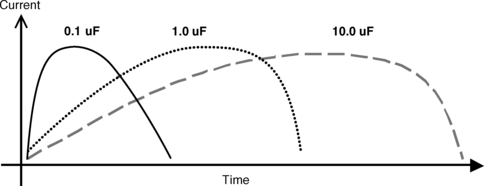
Mixed signal applications typically use a combination of bypass caps to address the low-frequency and high-frequency current demands. Capacitors with larger values tend to have larger values of associated inductance, so smaller caps in parallel provide a compound solution. A 10-uF tantalum cap in parallel with a 1.0-uF and 0.1-uF monolithic cap is a common choice.

The 0.1-uF capacitor has the lowest inductance, and responds immediately to the current demand. The 1.0-uF capacitor takes longer to respond, but can supply current for a longer period of time. The 10.0-uF capacitor has the highest inductance and the slowest response time, but can supply current for the duration of the transient current demand.
• Think about where the currents go.
• Conductors have resistance, inductance, and capacitance. So do resistors, capacitors, and inductors.
• Current that flows out of the device must come from somewhere.
• Current that flows into the device must go somewhere.
• Keep PC traces short and wide.
• Use ground planes, especially under components and traces that operate at high frequency.
• Use separate supplies and separate returns for the digital and analog sections. Tie the returns together at a single point.
• Physically separate analog and digital signal traces.
• Avoid crossovers between analog and digital signals.
• Be very careful with high impedance points. Consider the use of guard rings.
9.7 Transmission Lines
A transmission line is an interconnect consisting of two conductors and a dielectric. Characteristics include distributed series resistance and inductance, along with distributed parallel capacitance between the two conductors. Coax cable is a common example of a transmission line, but the same effects are evident with circuit board interconnect paths.
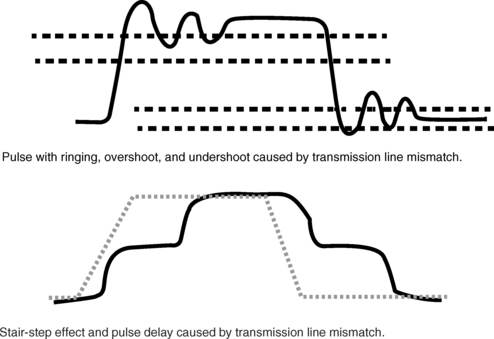
Transmission line impedance mismatch can result in signal delays or ringing at interconnects, which in turn cause timing errors or incorrect data.
9.7.1 Transmission Line Reflections
Transmission line effects are basically Ohm’s law across time. It takes a finite amount of time for a pulse to travel from one end of wire to the other. Between the time when the pulse is generated and when it gets to the end of the wire, the only impedance is the wire itself. The wire, or transmission line, impedance acts as a current load for a period equal to one round trip delay for each signal transition. The transmission line does not present any current load under DC conditions. If the load impedance does not match the transmission line impedance, the current differential causes a reflection from the load back to the source.
If the current differential is extreme, a transmission line with mismatched impedance can cause signal voltages to appear to double at the receiver termination.
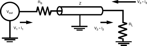
1. The initial condition of voltage and current is equal to V1 and I1 at the signal source.
2. The condition of voltage and current at the end of the transmission line is equal to V2 and I2 at the signal termination.
3. If the source and termination condition of voltage and current are not the same, the transmission line reflections are equal to V3 and I3.
Example
Transmission Line Impedance = 50 ohms Transmission line propagation delay = 5 ns
For the first 5 ns after the signal transition, the voltage source drives only the 50-ohm transmission line impedance. Driving 3 volts into 50 ohms requires 60 mA. This 3 volts at 60 mA flows down the transmission line until it encounters the termination of RL. Because the load impedance of 10 K across 3 volts absorbs only 0.3 mA, a reflected wave must be generated to satisfy Ohm’s Law. The reflected current goes back across the 50-ohm transmission line. The reflected current of 59.7 mA across the 50-ohm impedance produces a voltage step (E = I × R) of 2.98 volts, which is superimposed on the 3-volt signal from the source. The signal level effectively doubles because of the reflected current. The current continues to bounce back and forth between the source and the load until it is absorbed. Guess what? That’s what causes ringing.

The properties of the transmission line are described by the impedance (Z) and the propagation delay (Tpd). Both the transmission line impedance and the propagation delay are a function of the distributed inductance (L) and capacitance (C).
The reflection coefficients are a function of the ratios of source impedance, transmission line impedance, and the load impedance.
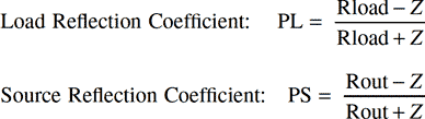
There are several combinations of source, transmission line, and load impedance that may occur in a test circuit.
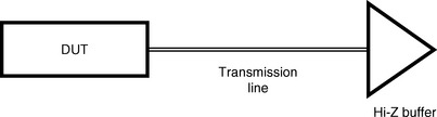
9.7.2 High Impedance Load Effects
1. A high-speed device output with corresponding high-current capability and a low value of Rout (5 ohms)
3. The input of a high-impedance buffer, with an input impedance of 1 MB ohm.
Calculate the load reflection coefficient.
Calculate the source reflection coefficient.
A transmission line with a positive load reflection coefficient (PL) will exhibit ringing, overshoot, and undershoot. A matched transmission line will approximate zero for both the load and the source reflection coefficients.

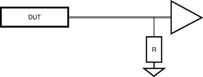
9.7.3 Low Impedance Load Effects
In some test circuit implementations, the transmission line may be terminated with a low impedance load.
Example
1. A high-speed device output with corresponding high-current capability and a low value of Rout (5 ohms)
Calculate the source reflection coefficient.
Calculate the load reflection coefficient.
A transmission line with a negative load reflection coefficient (PL) will exhibit a stair-step distortion or improper duration of the pulse period.
I ran into this phenomenon once with a video amp application, and it nearly drove me crazy. The output of the DUT was connected to a high-current buffer, which in turn drove a terminated coax cable to the receive circuit.

On the output of the DUT, the scope showed a nice, fat, reasonable-looking pulse. On the other side of the buffer, the signal had degraded into a skinny little glitch. My first instinct was to blame the hardware, so I replaced the buffer. That didn’t help, so I had to get more scientific. I noticed that if the buffer output was not connected to the transmission line, then the signal coming out of the buffer looked just fine. That gave me enough clues to suspect the transmission line, and here’s what I found:

Well, yeah, it is obvious now, but it sure wasn’t then. Let’s take a look at the coefficients.

Yep, that will do it, all right. In this case, I was able to change the receive impedance from 37.5 ohms to 50 ohms, and then re-calculate the expected voltage and current levels.
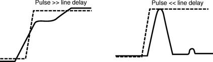
9.7.4 Edge Rate and Line Length
The effects of the transmission line vary based on the edge rate of the DUT and the propagation delay of the transmission line. If the device edge rate is short compared to the transmission line delay, the effects of the impedance mismatch become apparent. If the rise and fall time of the device is long in comparison to the transmission line delay, the effects are hidden during the transition time. In general, a PC board trace will act like a transmission line if the rise and fall time of the device is less than three times more than the transmission line delay. A circuit board trace designed to function as a transmission line is known as a “strip line.” The propagation delay for a strip line is approximately 2.5 ns per foot.
9.8 Transmission Line Matching
Designing a matched transmission line must take into account the source resistance, the transmission line impedance, and the load resistance. The source resistance must be less than or equal to the transmission line impedance (Z) to minimize the effect of the source coefficients. Secondly, the load resistance (RLoad) must be equal to the transmission line impedance (Z). A properly matched transmission line circuit has a load reflection coefficient (PL) of 0. There is no ringing or stair-step effect.
There are several alternatives for matching the transmission line to the source impedance and the load impedance, as follows:
(Note: The following examples use the abbreviation “TL” for Transmission Line.)
Also known as back matching, series termination inserts a resistor in series with the source to effectively change the value of Rout. This method has the advantage of simplicity, and is often the termination of choice when the transmission line impedance and the load impedance are fixed. The primary disadvantage is that series resistance (RB) limits the amount of available current, which can adversely affect the signal rise and fall time.

Parallel Termination Inserts a resistor in parallel with the RL at the end of the transmission line to change the value of RL. Parallel termination allows efficient absorption of the transient current, with no adverse effect on the signal transients. The two disadvantages are the constant DC load on the source, and asymmetrical loading. Asymmetrical loading is caused by a larger current demand for source high levels than for low levels.
Example
The source current when driving a logic high is equal to the VOH level divided by the termination resistance: 3.0 volts/50 ohms = 60 mA.
The source current when driving a logic low is equal to the VOL level divided by the termination resistance: 0.4 volts/50 ohms = 8 mA

Thevenin termination is similar to parallel termination, but replaces the single termination resistor (Rterm) with two resistors, one for the positive load and one for the negative load. The resistors are connected to respective IOL and IOH sources.
Thevenin termination allows efficient absorption of the transient current, without the asymmetrical loading problem of the simple parallel termination. There is still the disadvantage of a constant DC load.

Resistor-Capacitor termination is similar to parallel termination. A capacitor is placed between the termination resistor (Rterm) and ground to allow for a low impedance at AC without presenting a DC load. If all that a capacitor did was to block DC and pass AC, this would be an ideal solution. Unfortunately, another feature of a capacitor is that it will trap a charge. Because the capacitor stores a charge, it can distort the signal when discharging back into the transmission line.

Diode termination does not attempt to match the impedance, but rather conducts the reflected voltage and current to ground or VDD. This is the most effective termination method when the load circuit is accessible. Diode termination has an additional advantage because the activation energy for a silicon diode has a voltage-current ratio of approximately 50 ohms. Is that cool, or what?
