
Metallic Contaminants on Surfaces and Their Impact
Rajiv Kohli, The Aerospace Corporation, Houston, TX, United States
Abstract
Metallic contaminants are ubiquitous as discrete particles or in ionic form. Even in very low concentrations, they can adversely affect the performance of high-end devices. This chapter provides an overview of the sources and generation of metallic contaminants and discusses some of their impacts. Analytical techniques are briefly described that are available to detect and characterize metallic contaminants at the nanoscale.
Keywords
Contaminants; metallic contamination; diffusion; solubility; retrograde solubility; retrograde melting; defects; mitigation; cleanliness levels; impact; characterization techniques
1 Introduction
Metallic contaminants occur in nature as byproducts of natural processes where they are present in the starting materials for industrial products such as quartz used for manufacturing silicon-based devices, or as impurities in minerals used for producing high-end metal products. Metal contaminants are also produced as byproducts of human and industrial activity and can deposit on the surface of the product with detrimental effect. For example, in semiconductor silicon wafer processing, transition metal impurities in the wafer form metal silicide precipitates that can result in haze on the wafer surface. The performance of the device can be significantly degraded by metal impurities in the starting materials and metallic contaminants from the manufacturing process. In the case of a hard disk drive, a particle with dimensions of the order of the flying height between the recording head and the disk that is trapped between the head and the disk can cause catastrophic failure of the drive. Cationic contaminants also can lead to corrosion of the recording head and failure of the drive. The emphasis in this chapter will be on metallic contaminants deposited on the surface of products or present in the starting materials for products like semiconductor wafers and solar cells that are manufactured in controlled environments such as cleanrooms. Removal of contaminants has been covered previously and will not be addressed here. The discussion in this chapter is necessarily an overview of the broad and diverse subject matter and no attempt is made at comprehensiveness. A large number of general references address different aspects of metallic contamination and provide sources of additional information [1–41].
2 Cleanliness Levels
In the semiconductor industry, metallic contaminants at very low levels can adversely affect the performance of devices. Several standards and specifications have been issued that define allowable trace metal contamination levels in starting materials and on surfaces in the manufacturing environment.
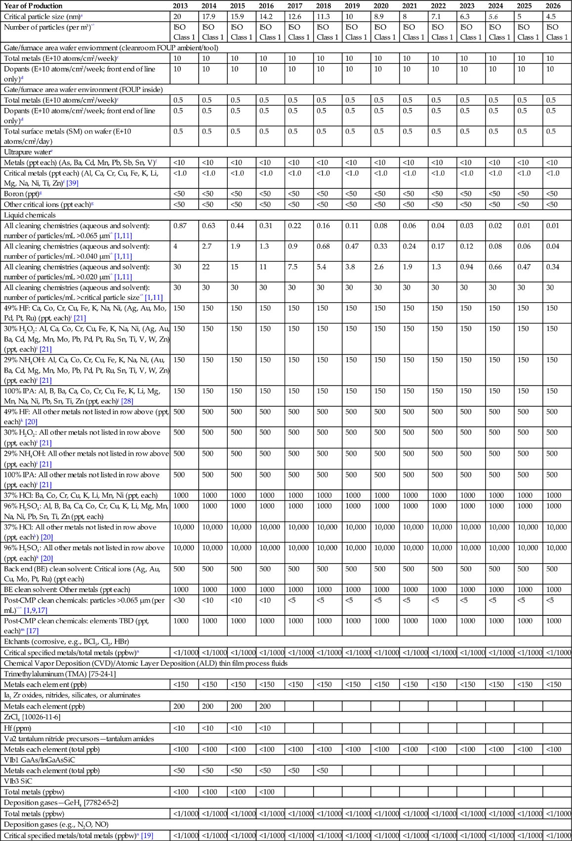
The most recent (2013) version of the International Technology Roadmap for Semiconductors (ITRS) lists maximum levels for trace metals in its 15-year projections to 2026 for a wide range of current and emerging semiconductor materials for various current and future device applications, including novel metal oxides, chalcogenides, graphene, carbon nanotubes, low-/high-k dielectric materials, and new and advanced materials, as well as process chemicals (Table 1.1) [42].
Table 1.1
ITRS Table YE3 Defines the Technology Requirements for Wafer Environmental Contamination Control Relative to Metal Contaminants [42]
| Year of Production | 2013 | 2014 | 2015 | 2016 | 2017 | 2018 | 2019 | 2020 | 2021 | 2022 | 2023 | 2024 | 2025 | 2026 |
| Critical particle size (nm)a | 20 | 17.9 | 15.9 | 14.2 | 12.6 | 11.3 | 10 | 8.9 | 8 | 7.1 | 6.3 | 5.6 | 5 | 4.5 |
| Number of particles (per m3)a,b | ISO Class 1 | ISO Class 1 | ISO Class 1 | ISO Class 1 | ISO Class 1 | ISO Class 1 | ISO Class 1 | ISO Class 1 | ISO Class 1 | ISO Class 1 | ISO Class 1 | ISO Class 1 | ISO Class 1 | ISO Class 1 |
| Gate/furnace area wafer enviornment (cleanroom FOUP ambient/tool) | ||||||||||||||
| Total metals (E+10 atoms/cm2/week)c | 10 | 10 | 10 | 10 | 10 | 10 | 10 | 10 | 10 | 10 | 10 | 10 | 10 | 10 |
| Dopants (E+10 atoms/cm2/week; front end of line only)d | 10 | 10 | 10 | 10 | 10 | 10 | 10 | 10 | 10 | 10 | 10 | 10 | 10 | 10 |
| Gate/furnace area wafer environment (FOUP inside) | ||||||||||||||
| Total metals (E+10 atoms/cm2/week)c | 0.5 | 0.5 | 0.5 | 0.5 | 0.5 | 0.5 | 0.5 | 0.5 | 0.5 | 0.5 | 0.5 | 0.5 | 0.5 | 0.5 |
| Dopants (E+10 atoms/cm2/week; front end of line only)d | 0.5 | 0.5 | 0.5 | 0.5 | 0.5 | 0.5 | 0.5 | 0.5 | 0.5 | 0.5 | 0.5 | 0.5 | 0.5 | 0.5 |
| Total surface metals (SM) on wafer (E+10 atoms/cm2/day) | 0.5 | 0.5 | 0.5 | 0.5 | 0.5 | 0.5 | 0.5 | 0.5 | 0.5 | 0.5 | 0.5 | 0.5 | 0.5 | 0.5 |
| Ultrapure watere | ||||||||||||||
| Metals (ppt each) (As, Ba, Cd, Mn, Pb, Sb, Sn, V)f | <10 | <10 | <10 | <10 | <10 | <10 | <10 | <10 | <10 | <10 | <10 | <10 | <10 | <10 |
| Critical metals (ppt each) (Al, Ca, Cr, Cu, Fe, K, Li, Mg, Na, Ni, Ti, Zn)f [39] | <1.0 | <1.0 | <1.0 | <1.0 | <1.0 | <1.0 | <1.0 | <1.0 | <1.0 | <1.0 | <1.0 | <1.0 | <1.0 | <1.0 |
| Boron (ppt)g | <50 | <50 | <50 | <50 | <50 | <50 | <50 | <50 | <50 | <50 | <50 | <50 | <50 | <50 |
| Other critical ions (ppt each)g | <50 | <50 | <50 | <50 | <50 | <50 | <50 | <50 | <50 | <50 | <50 | <50 | <50 | <50 |
| Liquid chemicals | ||||||||||||||
| All cleaning chemistries (aqueous and solvent): number of particles/mL >0.065 μma,h [1,11] | 0.87 | 0.63 | 0.44 | 0.31 | 0.22 | 0.16 | 0.11 | 0.08 | 0.06 | 0.04 | 0.03 | 0.02 | 0.01 | 0.01 |
| All cleaning chemistries (aqueous and solvent): number of particles/mL >0.040 μma,h [1,11] | 4 | 2.7 | 1.9 | 1.3 | 0.9 | 0.68 | 0.47 | 0.33 | 0.24 | 0.17 | 0.12 | 0.08 | 0.06 | 0.04 |
| All cleaning chemistries (aqueous and solvent): number of particles/mL >0.020 μma,h [1,11] | 30 | 22 | 15 | 11 | 7.5 | 5.4 | 3.8 | 2.6 | 1.9 | 1.3 | 0.94 | 0.66 | 0.47 | 0.34 |
| All cleaning chemistries (aqueous and solvent): number of particles/mL >critical particle sizea,h [1,11] | 30 | 30 | 30 | 30 | 30 | 30 | 30 | 30 | 30 | 30 | 30 | 30 | 30 | 30 |
| 49% HF: Ca, Co, Cr, Cu, Fe, K, Na, Ni, (Ag, Au, Mo, Pd, Pt, Ru) (ppt, each)i [21] | 150 | 150 | 150 | 150 | 150 | 150 | 150 | 150 | 150 | 150 | 150 | 150 | 150 | 150 |
| 30% H2O2: Al, Ca, Co, Cr, Cu, Fe, K, Na, Ni, (Ag, Au, Ba, Cd, Mg, Mn, Mo, Pb, Pd, Pt, Ru, Sn, Ti, V, W, Zn) (ppt, each)i [21] | 150 | 150 | 150 | 150 | 150 | 150 | 150 | 150 | 150 | 150 | 150 | 150 | 150 | 150 |
| 29% NH4OH: Al, Ca, Co, Cr, Cu, Fe, K, Na, Ni, (Au, Ba, Cd, Mg, Mn, Mo, Pb, Pd, Pt, Ru, Sn, Ti, V, W, Zn) (ppt, each)i [21] | 150 | 150 | 150 | 150 | 150 | 150 | 150 | 150 | 150 | 150 | 150 | 150 | 150 | 150 |
| 100% IPA: Al, B, Ba, Ca, Co, Cr, Cu, Fe, K, Li, Mg, Mn, Na, Ni, Pb, Sn, Ti, Zn (ppt, each)j [28] | 150 | 150 | 150 | 150 | 150 | 150 | 150 | 150 | 150 | 150 | 150 | 150 | 150 | 150 |
| 49% HF: All other metals not listed in row above (ppt, each)k [20] | 500 | 500 | 500 | 500 | 500 | 500 | 500 | 500 | 500 | 500 | 500 | 500 | 500 | 500 |
| 30% H2O2: All other metals not listed in row above (ppt, each)i [21] | 500 | 500 | 500 | 500 | 500 | 500 | 500 | 500 | 500 | 500 | 500 | 500 | 500 | 500 |
| 29% NH4OH: All other metals not listed in row above (ppt, each)i [21] | 500 | 500 | 500 | 500 | 500 | 500 | 500 | 500 | 500 | 500 | 500 | 500 | 500 | 500 |
| 100% IPA: All other metals not listed in row above (ppt, each)i [21] | 500 | 500 | 500 | 500 | 500 | 500 | 500 | 500 | 500 | 500 | 500 | 500 | 500 | 500 |
| 37% HCl: Ba, Co, Cr, Cu, K, Li, Mn, Ni (ppt, each) | 1000 | 1000 | 1000 | 1000 | 1000 | 1000 | 1000 | 1000 | 1000 | 1000 | 1000 | 1000 | 1000 | 1000 |
| 96% H2SO4: Al, B, Ba, Ca, Co, Cr, Cu, K, Li, Mg, Mn, Na, Ni, Pb, Sn, Ti, Zn (ppt, each) | 1000 | 1000 | 1000 | 1000 | 1000 | 1000 | 1000 | 1000 | 1000 | 1000 | 1000 | 1000 | 1000 | 1000 |
| 37% HCl: All other metals not listed in row above (ppt, eachk) [20] | 10,000 | 10,000 | 10,000 | 10,000 | 10,000 | 10,000 | 10,000 | 10,000 | 10,000 | 10,000 | 10,000 | 10,000 | 10,000 | 10,000 |
| 96% H2SO4: All other metals not listed in row above (ppt, each)k [20] | 10,000 | 10,000 | 10,000 | 10,000 | 10,000 | 10,000 | 10,000 | 10,000 | 10,000 | 10,000 | 10,000 | 10,000 | 10,000 | 10,000 |
| Back end (BE) clean solvent: Critical ions (Ag, Au, Cu, Mo, Pt, Ru) (ppt each) | 500 | 500 | 500 | 500 | 500 | 500 | 500 | 500 | 500 | 500 | 500 | 500 | 500 | 500 |
| BE clean solvent: Other metals (ppt each) | 1000 | 1000 | 1000 | 1000 | 1000 | 1000 | 1000 | 1000 | 1000 | 1000 | 1000 | 1000 | 1000 | 1000 |
| Post-CMP clean chemicals: particles >0.065 μm (per mL)a,l,m [1,9,17] | <30 | <10 | <10 | <10 | <5 | <5 | <5 | <5 | <5 | <5 | <5 | <5 | <5 | <5 |
| Post-CMP clean chemicals: elements TBD (ppt, each)m [17] | 1000 | 1000 | 1000 | 1000 | 1000 | 1000 | 1000 | 1000 | 1000 | 1000 | 1000 | 1000 | 1000 | 1000 |
| Etchants (corrosive, e.g., BCl3, Cl2, HBr) | ||||||||||||||
| Critical specified metals/total metals (ppbw)n | <1/1000 | <1/1000 | <1/1000 | <1/1000 | <1/1000 | <1/1000 | <1/1000 | <1/1000 | <1/1000 | <1/1000 | <1/1000 | <1/1000 | <1/1000 | <1/1000 |
| Chemical Vapor Deposition (CVD)/Atomic Layer Deposition (ALD) thin film process fluids | ||||||||||||||
| Trimethylaluminum (TMA) [75-24-1] | ||||||||||||||
| Metals each elem ent (ppb) | <150 | <150 | <150 | <150 | <150 | <150 | <150 | <150 | <150 | <150 | <150 | <150 | <150 | <150 |
| Ia3 Zr oxides, nitrides, silicates, or aluminates | ||||||||||||||
| Metals each element (ppb) | 200 | 200 | 200 | 200 | ||||||||||
| ZrCl4 [10026-11-6] | ||||||||||||||
| Hf (ppm) | <10 | <10 | <10 | <10 | ||||||||||
| Va2 tantalum nitride precursors—tantalum amides | ||||||||||||||
| Metals each element (total ppb) | <100 | <100 | <100 | <100 | <100 | <100 | <100 | <100 | <100 | <100 | <100 | <100 | <100 | <100 |
| VIb1 GaAs/InGaAsSiC | ||||||||||||||
| Metals each element (total ppb) | <50 | <50 | <50 | <50 | <50 | <50 | ||||||||
| VIb3 SiC | ||||||||||||||
| Total metals (ppbw) | <100 | <100 | <100 | <100 | ||||||||||
| Deposition gases—GeH4 [7782-65-2] | ||||||||||||||
| Total metals (ppbw) | <1/1000 | <1/1000 | <1/1000 | <1/1000 | <1/1000 | <1/1000 | <1/1000 | <1/1000 | <1/1000 | <1/1000 | <1/1000 | <1/1000 | <1/1000 | <1/1000 |
| Deposition gases (e.g., N2O, NO) | ||||||||||||||
| Critical specified metals/total metals (ppbw)n [19] | <1/1000 | <1/1000 | <1/1000 | <1/1000 | <1/1000 | <1/1000 | <1/1000 | <1/1000 | <1/1000 | <1/1000 | <1/1000 | <1/1000 | <1/1000 | <1/1000 |

[1] D. W. Cooper, “Comparing Three Environmental Particle Size Distributions”, J IES. 21–24, B124 (1991).
[2] D. Y. H. Pui and B.Y.H. Liu, “Advances in Instrumentation for Atmospheric Aerosol Measurement”, TSI J Part Instrument. 4 (2), 3–2 (1989).
[3] ISO 14644-1, Cleanrooms and Associated Controlled Environments—Part 1: Classification of Air Cleanliness.
[4] SEMI MF1982-1103 (previously ASTMF 1982–99e1), Standard Test Methods for Analyzing Organic Contaminants on Silicon Wafer Surfaces by Thermal Desorption Gas Chromatography, SEMI.
aCritical particle size is based on ½ design rule. All defect densities are “normalized” to critical particle size. Critical particle size does not necessarily mean “killer” particles. Because of instrumentation limitations, particle densities at the critical dimension for <90 nm will need to be estimated from measured densities of larger particles and an assumed particle size distribution or determined empirically and extrapolated. The particle size distribution will depend on the fluid (e.g., water, clean room air, gases), f(x)~1/xn (where x is the particle size, n=2.2 for air and other gases; n varies significantly for liquids from 1 to 4, and empirical determination is recommended).
bAirborne particle requirements are based on ISO 14644-1 at “at rest” [46].
cDetection of metals at the levels indicated will be dependent on sampling time and flow rate. Sticking coefficients vary widely for metals. It is generally believed that Cu has a sticking coefficient 10× of other metals, and therefore the guideline for Cu could be lower.
dIncludes P, B, As, and Sb.
eThe ultrapure water parameters provided in this table are applicable for the most critical process unless otherwise identified by additional footnotes. Further information can be found in the supplementary ITRS tables.
fValues based on FMEA Risk Priority Number 625. Users of the table are strongly encouraged to review the FMEA and adjust as necessary for local UPW and wafer monitoring frequency. Note that Ni risk assessment was updated for UPW, defining Ni as a critical metal.
gOther critical ions may include inorganic anions such as fluoride, chloride, nitrate, nitrite, phosphate, bromide, sulfate as well as ammonium. However, no reference was currently found that these ions in typical concentrations found in ultrapure water up to 50 ppt (parts per trillion) have any impact on the process. Phosphate specification level was defined at 20 ppt based on failure modes and effects analysis (FMEA). Also, for organic anions such as acetate, formate, propionate, citrate, and oxalate no harmful levels have been established up to now.
hAs of the current year's update, the finest sensitivity of commercial liquid particle sensors for chemicals is 0.065 µm, although measurement technology is being developed at 0.020 μm. Values obtained by these particle counters are not directly comparable to the roadmap values and need to be normalized to critical particle size values in the roadmap using the equation and methods of note (a) above. Interim solution to a higher sensitivity particle counter is to collect data over longer time period to provide greater precision in the data near the threshold sensitivity of the counter. Most benchmark data has been collected at point of delivery (POD) or point of entry (POE) and is the basis for the parameters. This particle counting efficiency is not taken into account, which may vary with the particle counter model, particle composition, chemicals, etc. It is based on actual data reported.
iElements listed that are not in parentheses may cause high or some risk to device quality and may often be present in process chemicals. Elements listed that are in parentheses may cause high risk to device quality but are not typically present in process chemicals.
jConcentrations higher than 100 ppb (parts per billion) could cause corrosion especially in back end of line processes.
kThe following is a complete list of metal ions of concern in certain liquid chemicals: Ag, Al, As, Au, Ba, Ca, Cd, Co, Cr, Cu, Fe, K, Li, Mg, Mn, Mo, Na, Ni, P, Pb, Pd, Pt, Ru, Sb, Sn, Sr, Ti, V, W, Zn.
lKey particle size for scratching particles depends on mean particle size of the slurry. The target level will be specific to the slurry and wafer geometry sensitivity.
mUncertain at this time is what target levels might be set given the variety of chemistries used in the industry and unknown sensitivity of the wafer to particles or ionic contamination in the chemical. This parameter is identified as a potentially critical one that should be considered and work is ongoing to define the correct levels.
nThe list of critical metals (e.g., Al, Ca, Cu, Fe, K, Mg, Na, Ni, Si) varies from process to process depending on the impact on electrical parameters such as gate oxide integrity or minority carrier lifetime, as well as mobility of the metal in the substrate. The metals listed in note (g) for liquid process chemicals are of concern, but the issues around metals in specialty gases are primarily around the potential for corrosion to add metal particles to the gas flow (e.g., Co, Fe, Ni, P). The potential for volatile species containing metals must be considered for each specialty gas but are generally not present in the bulk gases.
For the solar industry, Semiconductor Equipment and Materials International (SEMI) has issued a specification for the purity level of silicon feedstock material (Table 1.2) [43].
Table 1.2
SEMI Specification PV17-1012 for Solar Grade Silicon [43]
| Grade | I | II | III | IV |
| Acceptors | <1 ppba | <20 ppba | <300 ppba | <1000 ppba |
| B, Al | ||||
| Donors | <1 ppba | <20 ppba | <50 ppba | <720 ppba |
| P, As, Sb | ||||
| Transition metals | <10 ppba | <50 ppba | <100 ppba | <200 ppba |
| Ti, Cr, Fe, Ni, Cu, Zn, Mo | ||||
| Alkali and alkaline earth metals | <10 ppba | <50 ppba | <100 ppba | <4000 ppba |
| Na, K, Ca | ||||
| Bulk O | Not specified | Not specified | Not specified | Not specified |
| C | <0.3 ppma | <2 ppma | <5 ppma | <100 ppma |
| Total H | Low enough so that particles do not explode on heating | |||
| Total Cl | Low enough so that particles do not explode on heating | |||

This specification is designed to address elemental impurities in photovoltaic silicon feedstock, which can take many physical forms, including, e.g., granules, powders, polysilicon chunks, wafers, reclaimed silicon, and top and tail cuts from silicon boules. The purity level can have significant impact on solar cell efficiency as well as the productivity of some processes used to transform the silicon feedstock into solar cells.
Particle cleanliness levels for surfaces are typically based on the amount of specific or characteristic contaminant remaining on the surface after it has been cleaned, irrespective of the chemical constitution of the particle. The cleanliness levels are based on contamination levels established in industry standard IEST-STD-CC1246E (which replaced the original cleanliness standard MIL-STD-1246 [44]) for particles from Level 1 to Level 1000 [45]. In cleanroom environments, air cleanliness levels are specified in consensus standard ISO 14644 Part 1 for micrometer scale particles (>0.1 μm), and ISO 14644 Part 12 for nanoscale particles (<100 nm) [46,47]. These standards have been discussed in detail [39].
Many of the products and manufacturing processes are also sensitive to, or they can even be destroyed by, airborne molecular contaminants (AMCs) that are present due to external, process, or otherwise generated sources, making it essential to monitor and control these contaminants. An AMC is chemical contamination in the form of vapors or aerosols that can be organic or inorganic, and it includes everything from acids and bases to organometallic compounds and dopants [48,49]. A new standard, ISO 14644-10 [50], is now available as an international standard that defines the classification system for cleanliness of surfaces in cleanrooms with respect to the presence of chemical compounds or elements (including molecules, ions, atoms, and particles). The standard identifies at least eight categories of AMCs: acid (ac), base (ba), biotoxic (bt), condensable (cd), corrosive (cr), dopant (dp), total organic compounds (toc), and oxidant (ox), as well as individual substances or groups of substances. This standard is applicable to all solid surfaces in cleanrooms and associated controlled environments such as walls, ceilings, floors, working environment, tools, equipment, and devices.
3 Metallic Contaminant Behavior
Metallic contaminants originate primarily from liquid chemicals and water as well as from metal parts of the manufacturing process tool (furnace and melt crucibles), plumbing, and tubing. The most common metallic contaminants are iron, aluminum, copper, and nickel, as well as ionic metals such as the alkali metals sodium and potassium and the alkaline earths such as calcium and barium. They degrade metal oxide semiconductor gate stacks and reduce carrier lifetimes, depending on the metal. Higher tunneling current, lower charge-to-breakdown characteristics, and worse, stress-induced leakage current are observed even at low contamination levels. However, other less common metals, such as niobium and titanium, are also known to affect device performance. Niobium is very effective as a recombination center, and, in addition, it is prone to surface segregation [51].
Metallic contamination in semiconductors adversely affects device performance. As linewidths decrease the allowable levels of metal contamination become smaller. In current integrated circuits (ICs), the traces are so close together that a particle lying across a trace would cause a short circuit. The transition metals can be detected via the change they cause in lifetime or diffusion length, as these impurities create energy states in the bandgap of the semiconductor material. In state-of-the-art microelectronic manufacturing, inline control of metal contamination to concentration levels below 1011 atoms/cm2 is mandatory to avoid yield loss due to poor gate oxide quality.
In photovoltaic and solar cell applications, transition metals are known to severely affect the minority carrier diffusion length and solar cell efficiency. The threshold concentration of interstitial iron acceptable for solar cells is around 2 ×1012 cm−3. Copper and nickel can be tolerated in concentrations up to 1014–1016 cm−3, while heavier metals such as titanium or tungsten can degrade cell performance in concentrations as low as 1011–1012 cm−3. Several Si materials used for commercial-scale manufacturing of solar cells can contain as much as 1015 cm−3 of iron, and 1012–1014 cm−3 of several other transition metals. In fact, the majority of the transition metals are found in metal precipitates or in inclusions at grain boundaries or intragranular defects. The recombination activity per metal atom in this state is reduced and the tolerance of solar cells to metal contamination increases.
In the glass industry, to produce high-quality ultralow-loss fiber for optical applications, transition metal contamination of the starting materials should be maintained at the ng/g (ppb) level and even pg/g (ppt) depending on the impurity, whereas for short wavelength applications, the μg/g (ppm) level of impurities can be acceptable [52–55].
At the high temperatures of the manufacturing processes in the semiconductor industry, metal contaminants are often in the molten state. Their behavior in the liquid and solid states determines the degree of perfection achieved in crystal growth, and thereby the ultimate performance of the semiconductor devices, and the heat dissipation in ICs, following the operations of oxidation, vapor deposition, sputtering, or printing. Miniaturization and nanotechnology products are also limited by inadequate knowledge and control of the behavior of metal contaminants. Diffusion and solubility are key physical properties in the manufacturing process design.
3.1 Diffusion
The diffusion coefficient of a solute impurity in the solid and liquid phases is a fundamental quantity required to characterize mass transport rates. The mechanisms of impurity diffusion in the solid phase are well established. Diffusivity depends exponentially on the diffusion temperature and is generally defined by the Arrhenius equation:
(1.1)
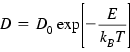 (1.1)
(1.1)Here D is the diffusivity in cm2/s; D0 is the temperature-independent preexponential factor in cm2/s; E is the diffusion activation energy in kJ/mol; kB is the Boltzmann constant; and T is the absolute temperature in degrees Kelvin.
By contrast, the mechanisms for diffusion in the liquid phase are not well understood and several theories have been proposed to explain the process that involve local density fluctuations in the liquid, viscosity of the liquid, molecular friction, free volume theory, hard sphere model, vibration models, and entropy correlation [56–59]. However, there are numerous difficulties in accurately measuring diffusion coefficients in liquid metals, primarily attributable to mass transport by bulk motion of the liquid due to natural convection. This is driven by buoyancy forces produced by any temperature or concentration gradients, which can lead to decrease of liquid density with depth. The relative dearth of experimental data for self-diffusion and solute diffusion in liquid metals and alloys compounds the problem of developing a theory that is universally applicable, which can accurately represent existing experimental data and which can predict diffusion coefficients when no experimental data are available.
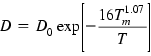
In terms of the temperature dependence, the Arrhenius equation is still widely used for solute diffusion in liquids. However, the preexponential factor and the activation energy are determined by fitting available experimental data, or are estimated from first-principle simulations and semiempirical correlations [60–75]. Several modified forms of the Arrhenius equation have been proposed to estimate solute diffusivity in liquid metals. One equation is based on numerical combination of equations derived from the fluctuation mechanism and the hard sphere mechanism, which yields the following equation [58,70]:
(1.2)
Here dA and dB are the Goldschmidt diameters of the atoms A and B, respectively; Tm is the melting point of the solute species in degrees Kelvin; K0 is the atomic valence of the solute species, defined as 1, 2, and 3 for body-centered cubic, hexagonal close-packed, and face-centered cubic structures, respectively.
Another predictive equation given below is based on combining the modified Stokes–Einstein–Sutherland formula with the melting point viscosity model [60,61,72–74].
(1.3)
 (1.3)
(1.3)
and
(1.4)
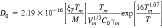 (1.4)
(1.4)
Here ξT is a correction factor introduced by the authors; Vm is the molar volume; C0 is a constant that is approximately the same for all metals (≈0.369 kg−1/2 m−1 s K1/2 mol1/2); γm is the surface tension.
These equations have been used to estimate impurity diffusion coefficients in the liquid phase for silicon as a function of temperature for several solute species for which experimental data are sparse or nonexistent [76].
Figs. 1.1–1.3 show the temperature dependence of the diffusivities of selected impurities in solid and liquid silicon and in solid germanium, plotted on a logarithmic scale as a function of the reciprocal temperature using critically assessed data and first-principle calculations to validate the experimental data [32,76–127]. Often the reported experimental values vary widely. For example, the reported activation energies vary from 12.54 to 409.1 kJ/mol (0.13–4.24 eV), while the preexponential factor ranges from 10−13 to 0.5 cm2/s for the diffusivity of interstitial nickel in crystalline silicon. Similarly, cobalt diffusion in silicon also shows large deviations in the preexponential factor (10−8 to 10−13) and the activation energy (35–269 kJ/mol) among the reported data using different measurement techniques [107].

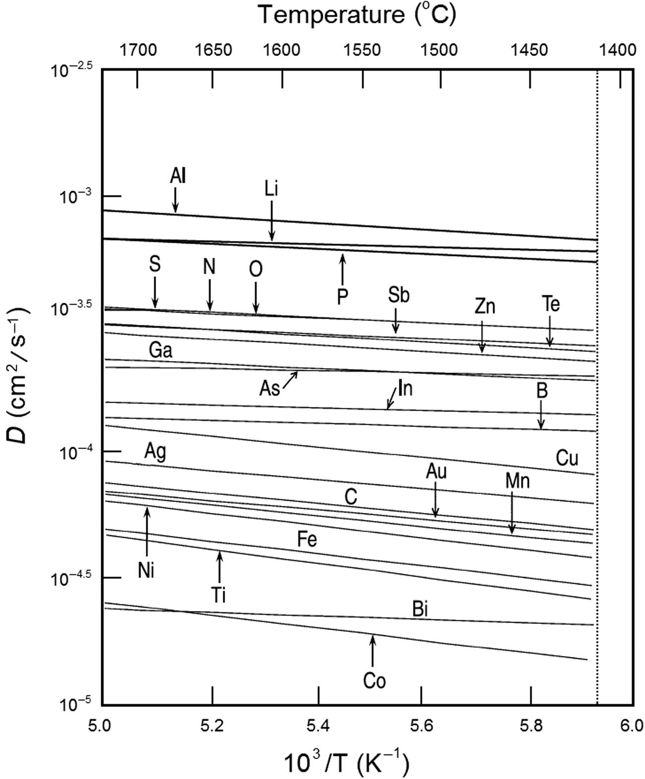

Diffusivity defines the time that is required for a solute impurity to reach thermal equilibrium. At low diffusivities, the solutes are prevented from reaching thermal equilibrium and will exist as quenched, metastable defects at room temperature. High diffusivities prevent the impurity solutes from forming such metastable defects, but can form precipitates on cooling. The transition metals, Co, Ni, Cu, and Pd, are among the fastest-diffusing solute impurities in silicon, with diffusion coefficients as high as 10−4–10−5 cm2/s at 800°C. At lower temperature the diffusivity of copper in silicon is even higher compared to other transition metals. Penetration of these impurities in a wafer of 500 μm thickness will take less than 10 seconds. During heat treatment, these metals form the respective silicide precipitates very rapidly on cooling, which then act as a diffusion source. For example, nickel diffuses outward so rapidly that more than half the surface of a 100-mm diameter wafer can be contaminated with haze after heat treatment for 20 minutes at 1050°C. Rhodium is known to form haze on the surface, and although its diffusivity in silicon is unknown, it is likely to be on the order of 10−6 cm2/s at 800°C, similar to Pd, which also forms haze [9,85]. This is a reason why these metal impurities are detrimental during wafer processing.
3.2 Solubility
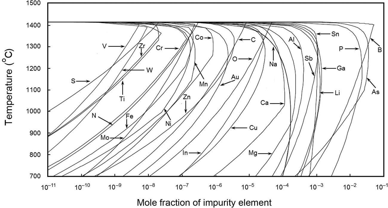
The solubility of a solute impurity is the maximum concentration of the solute that can be dissolved at thermal equilibrium in the sample at a given temperature without forming a second phase. It is temperature dependent and is represented by the solidus or liquidus boundaries in the respective phase diagrams. The phase diagrams provide information on the solubility and composition of the phases present in the system and the temperature at which these phases form [128]. In the case of solid silicon, the solubility of impurity elements ranges from parts per billion for the transition metals to few percent for the light elements (Fig. 1.4).
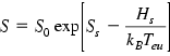
Below the eutectic temperature, the solubility S can be represented by the Arrhenius equation.
(1.5)
 (1.5)
(1.5)
Here S0 is the temperature-independent preexponential factor; Ss and Hs are the solution entropy and enthalpy, respectively; Teu is the eutectic temperature.
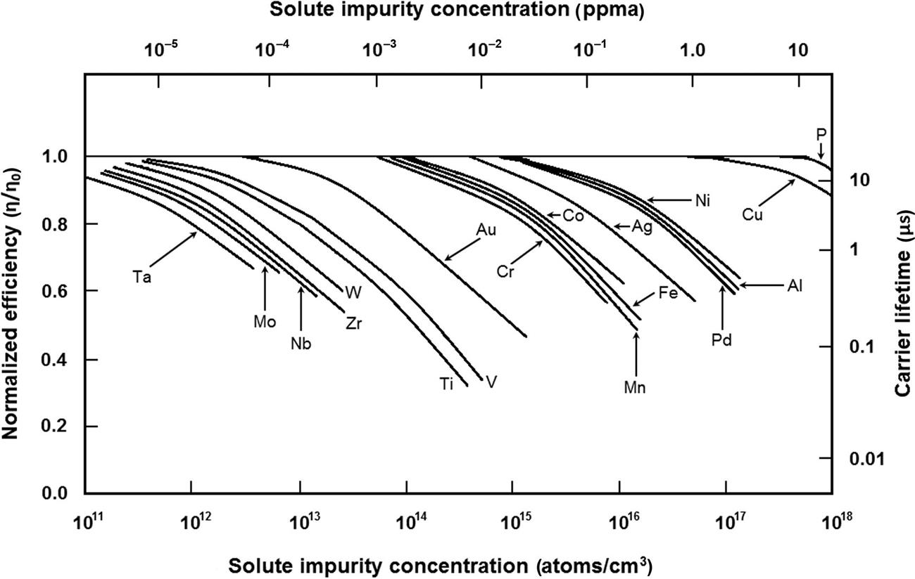
The solubility of an impurity atom differs by several orders of magnitude between room temperature and higher temperatures, such as a typical silicon process diffusion temperature of 1100°C, as well as the solubilities among the elements at the same temperature, as shown in Fig. 1.5 for the transition metals in silicon [9,111,115]. The very steep slopes of the Arrhenius plots indicate drastic reduction in the solubility at room temperature, resulting in precipitation of the impurity within the bulk, or rapid diffusion to the surface of impurities with high diffusion coefficients, where they can form silicide precipitates and haze. Of the 18 transition metals that have been investigated, Fe, Co, Ni, Cu, Pd, and Rh form haze [9,84,85]. If the impurity atoms remain within the bulk volume due to low diffusivity, they can form electrically active complexes with other impurities, resulting in deterioration of the device performance. Fig. 1.6 shows the impact of the concentration of various impurities on p-type silicon solar cell efficiency [95,101,118,129–131]. For example, Cu and Ni can be tolerated in concentrations at the sub-ppm level (~1014–1017 atoms/cm3), while heavier metals such as Mo, Ti, or W can degrade cell performance in concentrations as low as 1011–1012 atoms/cm3 and should be present at sub-ppb levels.

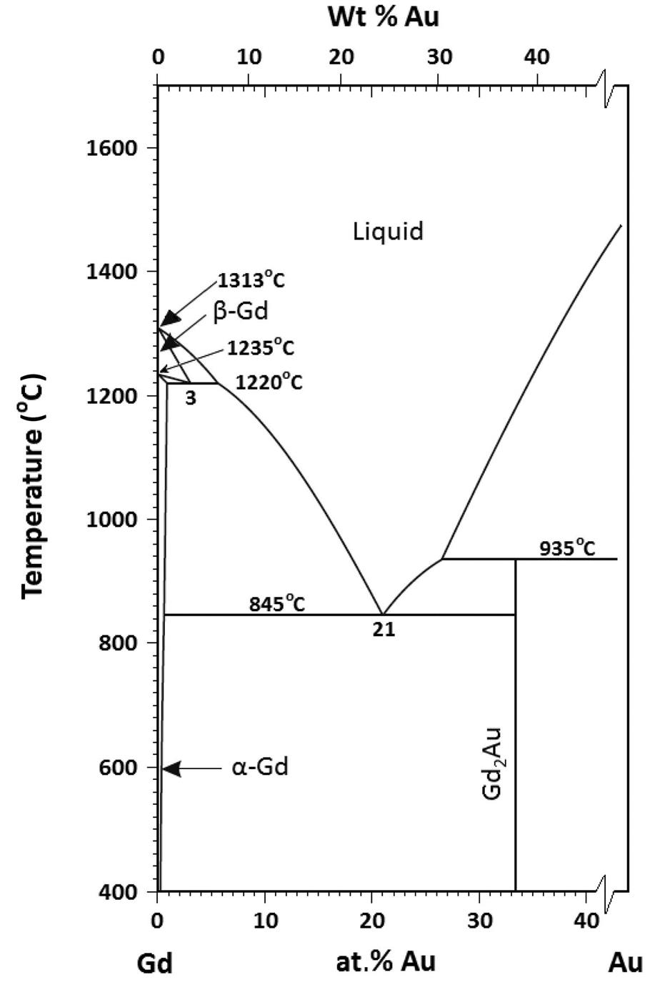
Above the eutectic temperature but below the melting temperature, the solubility is retrograde and describes the change in impurity concentration in the solid. The impurities tend to precipitate on cooling. Review of the phase diagrams shows that metatectic or catatectic phase reactions (solid (S1)→solid (S2)+liquid) occur in more than 50 binary metallic systems of technical interest, including Fe-Mn, Fe-S, Fe-Pu, Fe-Zr, Ag-In, Al-Li, and Mg-Bi, as well as several rare-earth and Si-metal systems [132–144]. Even organic systems exhibit retrograde melting [145–152]. As an example of a binary metallic system, consider the Gd-rich end of the phase diagram of the Gd+Au system shown in Fig. 1.7 [128,135]. This system exhibits a catatectic invariant at 1220°C. An alloy containing 2 at.% Au, when heated, will first melt at 845°C, will resolidify completely above 1220°C, and will begin to melt again at around 1242°C. The reverse process occurs on cooling.
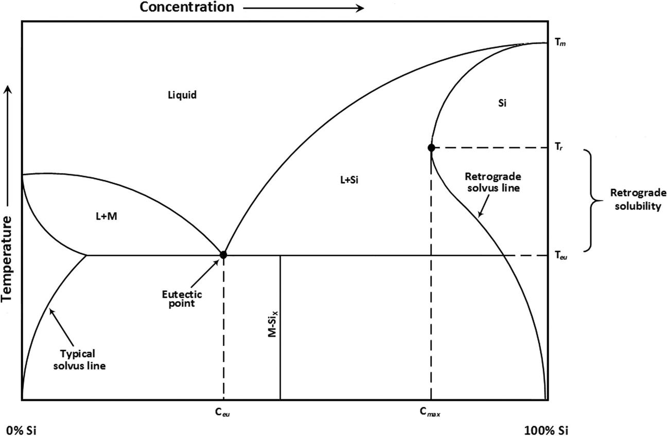
In most common silicon-impurity systems, retrograde melting cannot occur by this mechanism, since these systems do not exhibit a catatectic point [128,142,143]. An alternate pathway is illustrated in the generic silicon-metal phase diagram of Fig. 1.8. The solid solubility of an impurity within the crystal structure increases with temperature and reaches the maximum concentration well above the invariant reaction temperature (eutectic or peritectic), leading to supersaturated solutions. The metal solutes tend to form second-phase precipitates that are distributed throughout the solid matrix upon cooling. Since the supersaturated solutions exist at temperatures above the eutectic temperature, the precipitates form in the liquid phase causing retrograde melting, where local melting occurs upon cooling. The solubility of metal solutes in the liquid phase is much higher than in the solid phase, which results in solid-to-liquid gettering and reduces the concentration of impurities in the bulk.
Many dissolved elements in silicon exhibit such invariant behavior (Table 1.3), although other elements do not (Table 1.4). If supersaturation occurs above the eutectic temperature, second-phase particles can precipitate and can lead to retrograde melting [142,143]. The driving force for precipitation is the reduction in free energy per metal atom [136,137,143] and is given by
(1.6)
 (1.6)
(1.6)
Table 1.3
Estimated Driving Force for Selected Solutes that Exhibit Retrograde Solubility in Silicon [76,80,111,115,128,137,143]
| Solute | Invariant Temp. (°C) | Cinv (atoms/cm3) | Cmax (atoms/cm3) | ∆Fc (meV/atom) |
| Li | 592 | 4.5 × 10¹⁸ | 6.0 × 10¹⁹ | 193 |
| Cu | 802 | 6.0 × 10¹⁶ | 1.6 × 10¹⁸ | 304 |
| Ag | 835 | 1.8 × 10⁶ | 6.5 × 10¹⁶ | 2320 |
| Au | 363 | 8.6 × 10⁷ | 1.0 × 10¹⁷ | 1140 |
| Mg | 945 | 5.0 × 10¹⁸ | 1.5 × 10¹⁹ | 115 |
| Ca | 1030 | 2.4 × 10¹⁸ | 6.0 × 10¹⁸ | 103 |
| Zn | 420 | 1.3 × 10⁶ | 8.0 × 10¹⁶ | 1480 |
| Al | 577 | 9.0 × 10¹⁷ | 2.0 × 10¹⁹ | 227 |
| Ga | 30 | 1.1 × 10¹⁶ | 3.0 × 10¹⁹ | 206 |
| In | 156 | 2.1 × 10⁸ | 2.0 × 10¹⁸ | 851 |
| Sn | 232 | 7.0 × 10¹⁷ | 7.5 × 10¹⁹ | 203 |
| Sb | 630 | 2.0 × 10¹⁹ | 5.0 × 10¹⁹ | 197 |
| Bi | 271 | 1.0 × 10⁶ | 1.0 × 10¹⁸ | 1300 |
| S | 1202 | 1.7 × 10¹⁶ | 3.1 × 10¹⁶ | 76 |
| Mn | 1149 | 9.5 × 10¹⁵ | 3.5 × 10¹⁶ | 160 |
| Fe | 1207 | 1.6 × 10¹⁶ | 2.2 × 10¹⁶ | 41 |
| Co | 1259 | 2.8 × 10¹⁶ | 3.1 × 10¹⁶ | 13 |
| Ni | 993 | 2.2 × 10¹⁷ | 7.0 × 10¹⁷ | 126 |
| Pd | 892 | 3.0 × 10¹⁶ | 2.8 × 10¹⁷ | 224 |
| Pt | 970 | 5.9 × 10¹⁵ | 1.2 × 10¹⁷ | 323 |

Table 1.4
Elements with an Invariant Reaction at the Si-Rich End, but do not Exhibit Retrograde Solubility in Silicon [76,115,128,143]
| Solute | Invariant Temp. (°C) |
| B | 1385 |
| Sc | 945 |
| Ti | 577 |
| Zr | 1207 |
| As | 1149 |
| V | 1202 |
| Cr | 1030 |
| Mo | 1259 |
| W | 993 |
| U | 802 |
where ∆Fc is the driving force, Cmax is the actual solute concentration at the temperature of maximum solubility, and Cinv is the concentration of the solute at the invariant temperature.
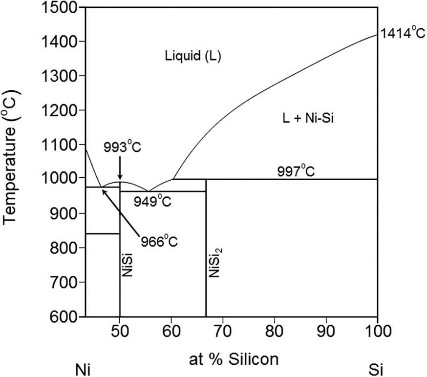
As shown in Table 1.3, several silicon-metal systems have large driving forces, especially at low invariant temperature, and are likely to exhibit retrograde melting. A good example is the Si-Ni system shown in Fig. 1.9. It has a large driving force and the invariant temperature (993°C) is 44 degrees higher than the eutectic temperature (949°C).
This phenomenon has been used for purification of metallurgical-grade silicon for use in solar cell applications [153–159], as well as for fabricating silicon nanowires and predictive control of the concentration and distribution of metal impurities in semiconductors [138,139,141–143,160–162]. However, retrograde melting can also lead to deleterious effects such as hot shortness or solidification cracking of welds in stainless steels [134,163–166], as well as diffusion-driven liquid metal embrittlement in susceptible systems [167–171].
4 Contamination Sources
4.1 Metal Impurities and Particles
In silicon processing, metal impurities may enter the starting materials from an external source that is directly or indirectly in contact with the melt or the cooling crystal, including furnace parts, growth surfaces, or feedstock [103]. Cu, Cr, Fe, Hf, Mn, Mo, Ni, and Ti have been observed. Metals can also diffuse from crucible walls directly into the Si ingot after crystallization [172–179]. Impurity concentrations can vary in the ingot and between different ingots processed in the same equipment. Therefore, it is critical to control all process parameters and impurity sources to ensure high-quality consistently reproducible material.
Trace metals can be introduced into a sample from containers that have been washed and rinsed in a conventional siphon-type washer as compared with washing in a high-efficiency washer designed to minimize trace metal contamination by first flushing the container with high-purity nitric acid, followed by rinsing with ASTM Type I water [180–182]. As Table 1.5 shows, conventional washing can introduce nearly two orders of magnitude higher levels of trace metal contamination in a process liquid compared with processing in a high-efficiency washer.
Table 1.5
Trace Metal Contamination of Redistilled Nitric Acid Processed in a Conventional Laboratory Environment Compared with the same Procedure Performed in a High-Efficiency Washer in a Cleanroom [180]
| Element (ppb) | Conventional Washer | High-Efficiency Washer | Detection Limit |
| Ag | 2.33 | <0.01 | 0.0088 |
| Al | 6.42 | <0.01 | 0.13 |
| Be | 2.62 | <0.01 | 0.007 |
| Bi | 1.07 | <0.01 | 0.0006 |
| Ca | 18.8 | <0.02 | 2.9 |
| Co | 2.02 | <0.01 | 0.004 |
| Cr | 0.91 | <0.04 | 0.28 |
| Fe | 1.62 | <0.02 | 0.75 |
| Mg | 2.56 | <0.01 | 0.016 |
| Mn | 1.72 | <0.01 | 0.012 |
| Na | 19.1 | <0.01 | 0.6 |
| Ni | 0.96 | <0.01 | 0.18 |
| Pb | 5.4 | <0.01 | 0.13 |
| Sn | 0.55 | <0.01 | 0.0033 |
| Th | 0.24 | <0.01 | 0.0003 |
| Ti | 0.56 | <0.02 | 0.003 |
| Tl | 1.53 | <0.02 | 0.0075 |
| Zn | 9 | <0.01 | 0.4 |

Common borosilicate glass has been found to release trace elements such as Na, Al, and B, especially at both extremes of pH, and is unsuitable for use in cleanroom manufacturing and processing activities. A much better but more expensive option is fused silica prepared from the vapor-phase hydrolysis of silicon tetrachloride or tetrafluoride. Fused silica can be cleaned effectively with acids and it can also be used at elevated temperatures. The trace metal contents of different kinds of silica are given in Table 1.6 [182–184].
Table 1.6
Content (ppm) of Selected Trace Impurities in Fused Silica
| Element | Transparent Silica from Quartz | Transparent SiX4 | Translucent Silica from Silica Sand |
| Al | 74 | <0.25 | 14–500 |
| B | 4 | 0.1 | 9 |
| Ca | 16 | <0.1 | 2.5–200 |
| Cr | 0.1 | 0.03 | nd |
| Cu | 1 | <0.05 | 0.5 |
| Fe | 7 | <0.2 | 1–77 |
| K | 6 | 0.1 | 1.7-37 |
| Li | 7 | 0.6 | 3 |
| Mg | 4 | <0.1 | 5–150 |
| Na | 9 | <0.1 | 2.5–60 |
| P | 0.01 | <0.001 | nd |
| Ti | 3 | <0.04 | 1–120 |

Polymers are widely used in semiconductor manufacturing. They can also be a source of trace metal contamination and should be carefully assessed for their suitability, especially contamination arising from residual catalysts and additives used in manufacture. The trace element content of some plastics is summarized in Table 1.7 [182].
Table 1.7
Trace Element Content of Various Plastics in Nanogram per Gram
| Element | LDPE | HDPE | PP | PS | PC | PVC | PTFE | FEP | ETFE |
| Al | 500 | 30,000 | 55,000 | 500 | 3000 | – | 230 | 200 | – |
| Au | – | – | 0.1 | 0.04 | 0.03 | – | 0.4 | – | 0.4 |
| Br | <20 | 800 | >5 | >1 | 29,000 | >6 | >2 | – | 240 |
| Ca | – | 800,000 | – | – | – | – | – | – | – |
| Cl | 7000 | 30,000 | 18,000 | – | 50,000 | major | – | 800 | 106 |
| Co | – | – | 40 | – | 6 | – | – | – | – |
| K | >5000 | >600 | – | – | – | – | – | 90,000 | 1100 |
| La | – | – | – | 0.3 | – | – | 0.6 | – | 1 |
| Mn | – | 10 | 20 | 20 | –– | – | – | 60 | – |
| Na | 1300 | 15,000 | 4800 | 2200 | 2700 | 20,000 | 160 | 400 | 600 |
| Sb | 5 | 200 | 600 | – | – | – | – | – | – |
| Sn | – | – | – | – | – | 2.4 × 10⁶ | – | – | – |
| Ti | – | 5000 | 60,000 | 1000 | – | – | – | – | – |
| W | – | – | – | – | – | – | – | 700 | – |
| Zn | – | 520,000 | – | – | – | – | – | – | – |
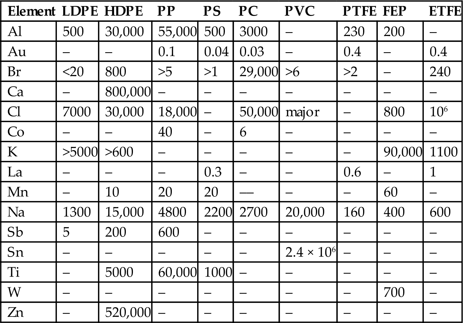
ETFE, ethylenetetrafluoroethylene; FEP, fluorinated ethylene propylene; HDPE, high-density polyethylene; LDPE, low-density polyethylene; PC, polycarbonate; PP, polypropylene; PS, polystyrene; PTFE, polytetrafluoroethylene; PVC, poly(vinyl chloride).
Particles are generated by human or industrial activities from expended energy that may be mechanical, chemical, thermal, electrical, or radiological in nature. Table 1.8 shows typical sources and sizes of particles from common activities. If the materials involved in these activities are metals or have a large metal content, the generated particles become a source of metal contaminants.
Table 1.8
Typical Size of Particles from Common Contamination-Generating Activities [39]
| No. | Activity | Typical Particle Size (µm) |
| 1 | Rubbing ordinary painted surface | 90 |
| 2 | Sliding metal surfaces (nonlubricated) | 75 |
| 3 | Crumbling or folding paper | 65 |
| 4 | Rubbing an epoxy-coated surface | 40 |
| 5 | Seating screws | 30 |
| 6 | Belt drive | 30 |
| 7 | Writing with ballpoint pen on ordinary paper | 20 |
| 8 | Handling passivated metals (e.g., fasteners) | 10 |
| 9 | Vinyl fitting abraded by a wrench or similar tool | 8 |
| 10 | Rubbing or abrading the skin | 4 |
| 11 | Soldering | 3 |
Many modern high-technology processes demand cleanliness of the product, the production environment, and the assembly process. Specifically, they demand an absence of particulate contamination. For example, in semiconductor manufacturing, the size of the contaminant airborne particles that must be filtered is equal to and larger than the feature size on the ICs; particles smaller than the feature size are not big enough to cause a short circuit or other particle-related failure. ICs are multilayered devices, with each layer being extremely thin. The density of IC surface areas compounds the likelihood that stray particles could destroy the entire chip. Controlling or eliminating particle contamination within the production environment is the primary concern of a semiconductor manufacturer.
The pharmaceutical industry commonly manufactures parenteral drugs. Parenteral (injectable) drugs must be free of particles (metallic and nonmetallic) and impurities that could infect the body—either human or animal [185]. Particles that can negatively affect the body tend to be larger than 2.0 or 3.0 μm and the pharmaceutical industry, like the semiconductor manufacturer, must manage the production environment to eliminate particle contamination. Typically, pharmaceutical companies determine process cleanliness by monitoring 0.5-μm particles and determine product sterility by monitoring 5-μm particles. In contrast, semiconductor manufacturing tends to concentrate on particles from 0.05 to 0.3 μm.
A major source of contaminant particles is the manufacturing process. Even in the highest quality cleanroom environment in nonoperational mode, particles will always be present, particularly nanosize particles. The current cleanliness specification for an ISO Class 1 cleanroom allows 10 particles of 0.1 µm (100 nm) size per cubic meter of air and 1200 particles of 10 nm size per cubic meter of air in the facility, regardless of the chemical nature of the particles [46,47]. Manufacturing operations performed in the cleanroom will change the environment relative to the number, size, range, and the physical and chemical characteristics of the particles. For example, the tools used to assemble a product are fabricated from materials that will wear with use. Also, the presence of people in the assembly process in a cleanroom or other controlled environment is itself a source of contamination. Particles are generated from human activity by shedding skin cells, emitting perfume/colognes/hairsprays, losing hair, breathing, and sneezing, among other activities. These particles contain elemental chemicals (Table 1.9) that can cause deleterious effects such as corrosion of the product [39].
Table 1.9
Undesirable Chemical Elements in Some Human Contaminants
| Contaminating Item | Elements |
| Spittle | K, P, Mg, Na, Cl− |
| Dandruff | Ca, C, N, Cl− |
| Perspiration | Na, K, S, Al, C, N, Cl− |
| Fingerprints | Na, K, P, Cl− |
| Lipstick | Bi, Si, Mg |
| Blush | Ti, Fe, Mg, Si, Al, K |
| Eye shadow | Bi, Si, Mg, Fe, Al |
| Mascara | Fe, Al, C |
| Cologne | Na, Si, N, Cl− |
Incoming parts used to assemble the final product can contribute significantly to particle contamination. Typical surface defects that are sources of particles include burrs, roughness, flaking, porosity, inclusions, and loose debris. There is an ongoing effort throughout the industry to eliminate the sources of these defects from incoming parts, but in many applications it is physically or financially impossible to eliminate these sources entirely.
Moving parts in a product create a tribological system that can generate metal particles due to friction and wear. Both these phenomena depend on many different factors, including surface and intrinsic properties of the contacting surfaces, mechanical and physical properties, and microstructural characteristics. At the macroscale, the laws of friction and wear are well established. Typical mechanisms generating particles are abrasive, erosive, adhesive, fatigue, plastic flow, corrosive, diffusive and melting wear, several of which can occur simultaneously in the contact region. At the nanoscale, friction and wear behavior of materials is very different. For example, the frictional force between two nanoscopically smooth surfaces depends on the area of contact of the surfaces. If the area of contact is sufficiently small, the load can be increased without increasing friction, resulting in less wear and reduced particle generation. This phenomenon can also be facilitated by nanoscale additives [186–188]. This is significant for many interfaces of technological importance such as microelectromechanical systems (MEMS) and hard disk drives with flying heights of 1–5 nm. The tribological implications of particles have been reviewed recently [189].
Another source of metal contamination is the growth of whiskers, which affects the reliability of a wide range of products from cardiac pacemakers and watches to missile systems and satellites, and have even resulted in the shutdown of a nuclear reactor [190–195]. The general reliability risks are short circuits, low-pressure-induced metal vapor arcing, and debris contamination, which can interfere with the performance of sensitive components. Whiskers are hairlike, single-crystal structures of various metals (such as Al, Au, Ag, Cd, In, Mo, Sb, Sn, Ta, W, and Zn), alloys, and metal oxides, which grow spontaneously from the surface of the material (Fig. 1.10). They can grow as kinked, bent or striated needles, or may take odd shapes. Whiskers are typically 1 nm to 30 μm in diameter, but they can grow from 100 μm to 10 mm in length. The primary mechanism for whisker formation is attributed to mechanical stresses on the surface that are relieved by whisker growth. Recently, an alternative mechanism has been proposed in which whisker formation is attributed to the energy gain due to electrostatic polarization of metal filaments in the electric field. The field is induced by surface imperfections such as contamination, oxidation states, and grain boundaries [196].

4.2 Ionic Contamination
Ionic contamination refers to the presence of undesirable cationic (such as Na+ and K+) and anionic (such as Cl−, F−, Br−, ![]() ,
, ![]() , and
, and ![]() ) ions from production processes (e.g., fluxes used during soldering, plating, chemical mechanical polishing, and photolithography), human activity, environment, and materials and chemicals that come in contact with the manufactured product. The ions can cause chemical, electrochemical, or galvanic corrosion of a part.
) ions from production processes (e.g., fluxes used during soldering, plating, chemical mechanical polishing, and photolithography), human activity, environment, and materials and chemicals that come in contact with the manufactured product. The ions can cause chemical, electrochemical, or galvanic corrosion of a part.
The sources of ionic contamination are varied. In general, ionic contamination can be classified as coming from the processes, people and objects that come in contact with the manufactured product. Ionic contamination includes ions in chemicals, ions deposited during handling, ions from the air, ions from cleaning products and equipment, and ions from packaging materials. For example, isopropyl alcohol used for cleaning may contain enough water to transfer the ionic contaminant to the part from the medium used for cleaning.
Some of the most common sources of ionic residue in the manufacture of printed wiring boards include plating chemicals, flux activators, human perspiration and fingerprints, component packaging materials, ionic surfactants and alkaline cleaning solutions, and ethanolamines used in cleaning products. In the presence of moisture, ionic residues can dissociate into either negatively or positively charged species and increase the overall conductivity of the solution, resulting in corrosion or metal deposition in the form of dendrites [197–200].
5 Characterization Techniques
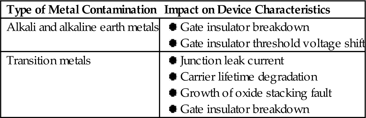
Metallic contaminants or impurities frequently occur in relatively low concentrations. There are two types of metal contamination, alkali and alkaline earth metals and transition metals, which have different impacts on electronic device characteristics (Table 1.10).
Table 1.10
Impact of Metal Contamination on Electronic Device Characteristics
| Type of Metal Contamination | Impact on Device Characteristics |
| Alkali and alkaline earth metals | |
| Transition metals |
The degree of contamination impact on device performance depends on the type of device. Table 1.11 lists the tolerable level of metal contamination on the surface, ranging from 108 atoms/cm2 for image sensors to below 1010 atoms/cm2 for photovoltaic devices and MEMS.
Table 1.11
Tolerable Level of Metal Contamination for Different Semiconductor Devices
| Type of Device | Tolerable Level of Metal Contamination (atoms/cm2) |
| Image sensor (complementary metal oxide semiconductor image sensor, charge-coupled device) | 1 to 5 ×10⁸ |
| Flash memory, dynamic random-access memory | 1 to 5 ×10⁹ |
| Power device (Si, SiC, GaN) | 1 to 5 ×10¹⁰ |
| Logic device | 0.5 to 5 ×10¹⁰ |
| Photovoltaic devices (Si crystal) | 1 to 5 ×10¹⁰ |
| Microelectromechanical systems | 5 ×10¹⁰ |
| Light-emitting diodes | 5 ×10¹⁰ |
The most common categories of trace metal contaminants are given below according to the source:
![]() Contaminants in the starting material. In silicon, total metals range from approximately 1 to 10 ng/g (ppm) for high-purity solar grade polysilicon, to 0.1–1% for metallurgical grade polysilicon.
Contaminants in the starting material. In silicon, total metals range from approximately 1 to 10 ng/g (ppm) for high-purity solar grade polysilicon, to 0.1–1% for metallurgical grade polysilicon.
![]() Process-related metal contaminants that are linked to the manufacturing processes and equipment, the environment, and human activity. They can be present as discrete metal particles in the submicrometer to macro size range, or as metal ionic contamination such as Na+ and K+.
Process-related metal contaminants that are linked to the manufacturing processes and equipment, the environment, and human activity. They can be present as discrete metal particles in the submicrometer to macro size range, or as metal ionic contamination such as Na+ and K+.
Depending on the purity of the starting materials and the manufacturing process, contaminants from either category can become the limiting factor for contamination control for the product. In semiconductors the concentration of metals is typically below 1010 atoms/cm3. This equates to a surface density of 3 ×10² for a silicon surface. Several characterization techniques [9,201,202] have been developed and applied successfully to identify and quantitatively analyze such small volumes. Contaminants in the starting material can be tested by bulk digestion for bulk trace metals or by surface extraction for surface trace metals. Analytical techniques, such as total reflection X-ray fluorescence spectrometry (TXRF) and inductively coupled plasma mass spectrometry (ICP-MS) in combination with wet chemical preconcentration procedures, or direct TXRF without chemical preconcentration, are widely applied for metallic contamination monitoring. The detection limit of TXRF or ICP-MS for metal contamination can be improved by vapor-phase decomposition droplet collection (VPD-DC). During the VPD step, HF vapor is used to etch the native oxide on the silicon surface in order to obtain a hydrophobic surface termination and the microdroplet is analyzed directly by ICP-MS, or it is dried for TXRF measurements [203–207].
Contaminant particles in the manufacturing environment can range from 0.001 to 100 µm; however, particles larger than 100 μm and smaller than 0.01 μm are of little interest to most modern manufacturing processes because particles larger than 100 μm are easily filtered and particles smaller than 0.01 μm are generally too small to directly cause contamination-related failures. Process-related contamination can be monitored with the same testing methods by strategically designing the test points before and/or after critical process steps to pinpoint the contaminating steps and identify the potential source of contamination.
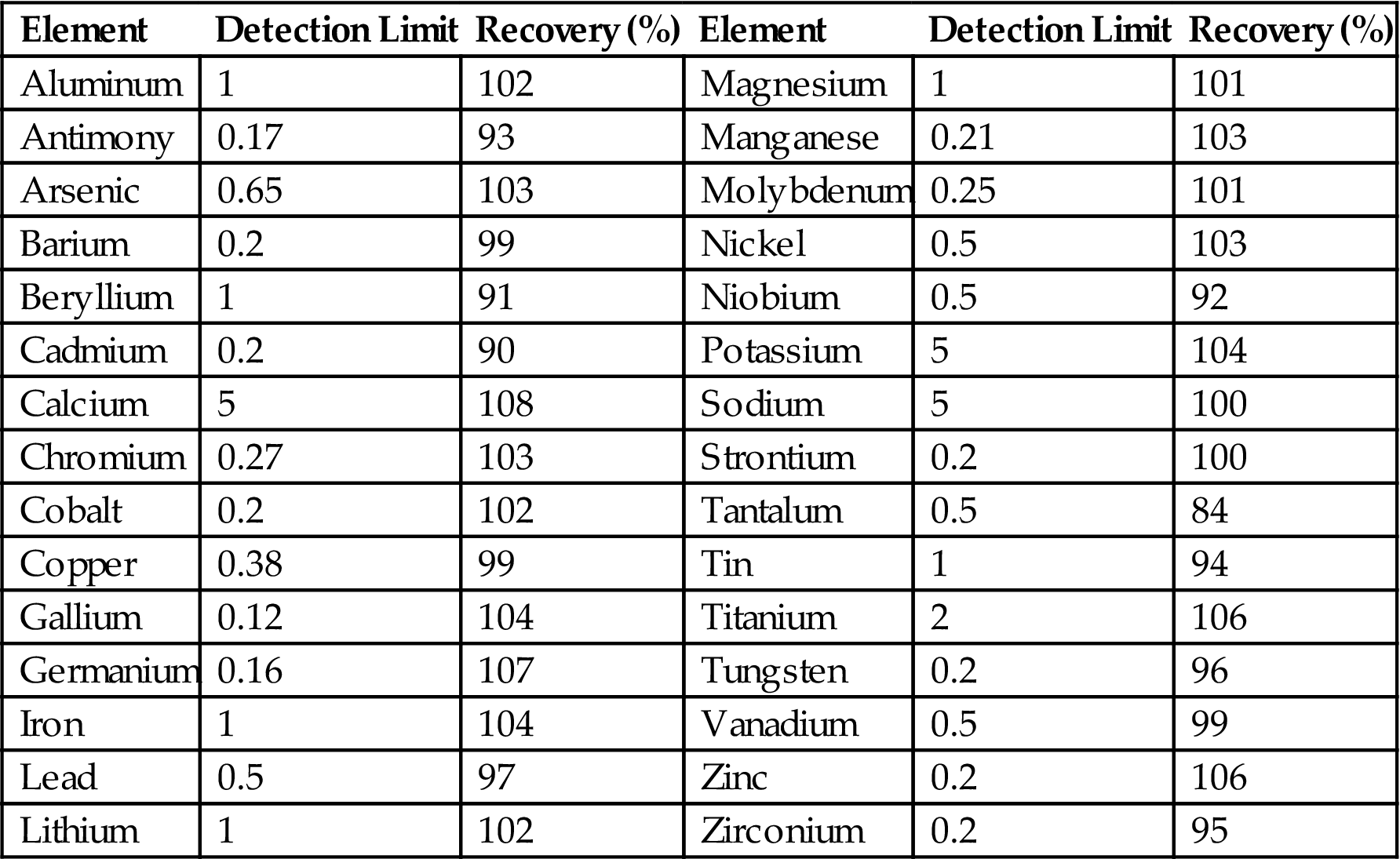
Mass spectroscopy techniques, such as secondary ion mass spectroscopy (SIMS) and glow-discharge mass spectroscopy, can be used effectively to access trace metals at low concentration levels on the surface (Table 1.12) [208–217]. Surface analysis techniques, such as SIMS, Auger electron spectroscopy, X-ray photoelectron spectroscopy, electron energy-loss spectroscopy, and atom probe tomography, can be used for studying impurity segregation to grain boundaries using highly focused beams [218–221].
Table 1.12
Detection Limit (ng/g) and Percent Recovery in Analysis of Trace Elements in Polysilicon by ICP-MS [214–216]
| Element | Detection Limit | Recovery (%) | Element | Detection Limit | Recovery (%) |
| Aluminum | 1 | 102 | Magnesium | 1 | 101 |
| Antimony | 0.17 | 93 | Manganese | 0.21 | 103 |
| Arsenic | 0.65 | 103 | Molybdenum | 0.25 | 101 |
| Barium | 0.2 | 99 | Nickel | 0.5 | 103 |
| Beryllium | 1 | 91 | Niobium | 0.5 | 92 |
| Cadmium | 0.2 | 90 | Potassium | 5 | 104 |
| Calcium | 5 | 108 | Sodium | 5 | 100 |
| Chromium | 0.27 | 103 | Strontium | 0.2 | 100 |
| Cobalt | 0.2 | 102 | Tantalum | 0.5 | 84 |
| Copper | 0.38 | 99 | Tin | 1 | 94 |
| Gallium | 0.12 | 104 | Titanium | 2 | 106 |
| Germanium | 0.16 | 107 | Tungsten | 0.2 | 96 |
| Iron | 1 | 104 | Vanadium | 0.5 | 99 |
| Lead | 0.5 | 97 | Zinc | 0.2 | 106 |
| Lithium | 1 | 102 | Zirconium | 0.2 | 95 |
Neutron activation analysis (NAA) has been successfully applied to identifying metals in silicon [97,102,222–226]. The major advantage of NAA is that it provides accurate results for large, bulk samples (tens of grams) without having to dissolve or digest the sample. NAA is an excellent complement to surface analysis techniques, such as TXRF, SIMS, and VPD-ICP-MS, in that it can provide similar sensitivities on large, bulk silicon samples, but no information is provided about the chemical states of the elements or their spatial resolution. The detection limits for the transition metals are highly dependent on the target species and range from 0.01 ppb (Au) to 1000 ppb (Nb) in a 100-mg sample. Analysis requires access to a high-flux neutron source and an isotope laboratory, and may take weeks or months until the results are available from the external laboratory, which makes it inconvenient to employ NAA for routine analysis and monitoring.
Several synchrotron-based X-ray fluorescence techniques have also been successfully applied to metal impurities in silicon and other semiconductors (such as GaN) and other solar grade materials [103,108,227–242]. X-ray fluorescence microscopy and its most recent electrical characterization complements, such as X-ray beam-induced current and X-ray beam-excited scanning optical luminescence microscopy, have enabled rapid acquisition of optical spectra in a wide spectral region with micrometer-scale spatial resolution. The spatial resolution has been extended into the nanometer scale with a high-resolution microprobe (beam spot size below 100 nm), which is used to locate metal-rich particles and precipitates and to determine their elemental composition and dimensions and their spatial distribution [103,240–242]. An ultrabright X-ray beam (108–1012 photons/s) produced by a synchrotron and focused down to a spot size of 80 nm provides the high-flux density necessary to detect and characterize nanometer-sized precipitates (~10 nm) and other intragranular defects such as dislocations [103,240–242]. By plotting the magnitude of a characteristic fluorescence peak of the individual element at each point on the sample, a two-dimensional map of the impurity distribution can be generated. The chemical state of the precipitates can be determined by X-ray absorption microscopy.
Methods based on measuring the carrier lifetime before and after defect transformation can also be very sensitive for certain impurities in p-type silicon, including B, O, Au, Cr, Cu, Fe, Mn, Mo, Ni, Ti, and V [118,129,130,243–250]. The impurities can be detected through diffusion length or lifetime measurements before and after thermal dissociation of the impurity defect, or optical dissociation of the impurity defect by strong illumination using surface photovoltage (SPV). Detection limits as low as 1010 cm−3 have been achieved and elemental maps can be developed by point-by-point lifetime measurements before and after dissociation of the defect. The SPV method can be used as a fast (5 minutes), practically preparation-free large area (25 cm2) detection method for impurities in Si and it can be used for routine monitoring of large numbers of wafers. SPV has also been used to monitor heavy metal contaminants during chemical cleaning of silicon wafers [244].
Some of the most sensitive techniques for detecting metal impurities in semiconductors, such as electron beam–induced current microscopy, deep-level transient spectroscopy (DLTS), and the Hall effect, are based on electrical measurements [17,25,129,136,251–258]. In principle, metal analysis at the parts per trillion level or better can be achieved. However, these techniques are primarily used to detect pointlike impurities, and interpretation of the spectra becomes challenging if precipitates are also present. Also, these techniques are quite time consuming and they only sample small specimen volumes (typically 104 μm3 to 1 cm3), which is far from ideal for large-scale monitoring purposes. Despite these challenges, a number of successful applications of DLTS have been reported for impurities in silicon and germanium, including chromium, manganese, iron, cobalt, vanadium, titanium, zinc, and zirconium.
Recently, methods for rapid imaging of carrier lifetimes of silicon wafers have been developed that have been used for detecting impurities and analyzing intragranular defects, as well as determining diffusion lengths and carrier lifetimes [259–267]. These lifetime imaging techniques, such as photoluminescence (PL) imaging and carrier density imaging, reduce the time required for a high-resolution map from hours for conventional carrier lifetime measurement methods (point-by-point mapping) to seconds for PL imaging. At these speeds, PL imaging is fast enough to be used as an inline tool for spatially resolved characterization in the manufacturing process. A recent advance has been the development of PL tomography, which provides three-dimensional maps of defect structures in semiconductors [268].
Several innovative methods have been developed for online monitoring of metallic contaminants. These methods include Hall effect sensors for measuring metal particle contamination in lubricants [269,270]; a contaminant-detection system using high-Tc superconducting quantum interference devices for foods and industrial products [271–273]; potentiometric sensors for detecting trace metal ion contamination at the parts per billion to parts per trillion level in process chemicals such as HF, alkaline H2O2, and ultrapure water [274,275]; and inductive coil sensors for online and field oil-condition monitoring for ferromagnetic and nonferromagnetic wear metal debris [276,277].
6 Impact of Metallic Contaminants
Surface contaminants can significantly affect the performance of high-technology precision products manufactured in controlled environments.
6.1 Metal Particles and Trace Metal Impurities
From a contamination perspective, nanosize metal particles can have major impact on the performance of precision and other products. For example, the presence of undesirable trace metal impurities such as nickel or iron in the parts per billion range can result in irrecoverable loss of the entire production lot of semiconductor wafers or degraded performance of the device fabricated from the wafers.
To develop mitigation and remediation strategies for small particle contamination, it is necessary to resolve the particles by their sizes [202]. Discrete particles can be generally classified by size according to Table 1.13.
Table 1.13
Range of Particle Sizes and Selected Techniques for Resolution of Particles
| Particle Class | Particle Size (nm) | Resolution Technique |
| Macro | >50,000 | Naked eye |
| Micro | >100 to 50,000 | Conventional optical microscopy |
| Submicro | 10 to 100 | Near-field optical microscopy, surface plasmon microscopy |
| Nano | >1 to 100 | Electron and probe microscopies |
| Atomic | 0.01 to 1 | Electron and probe microscopies, holography, resonance force microscopy |
| Subatomic | <0.01 | Femtosecond to attosecond spectroscopy, atomic force microscopy |
The challenges associated with accurately determining atomic positions at the nanoscale are formidable because atom positions must be known to very high precision, of the order of 0.01–0.001 Å (1 Å=10−10 m) needed for theoretical calculations of electronic structure and the functional properties of nanostructured materials [278–280]. A major advance in this direction has been to demonstrate measurement of atomic positions at a precision of 0.04–0.06 Å in aberration-corrected scanning transmission electron microscopes [281–284], which can be combined with statistical parameter estimation theory to determine atomic structural information for atoms and crystalline nanoparticles [285–287]. Similar levels of precision of atomic positions have been demonstrated by neutron holography [288].
In referring to very small particles, the size of the particles can be discussed in terms of various physical phenomena. For example, the interactions of particles much larger than 1 μm diameter are dominated by gravitational forces, while van der Waals and other forces tend to dominate their interactions below that size. Particles with diameters of 0.3–0.7 μm are of the same size as the wavelength of visible light, which is the limit of resolution in optical microscopic observation of particles in that size range. Particles in the size range 20–100 nm are referred to as ultrafine, while nanosize particles have diameters smaller than 20 nm. Due to the need to understand aerosol behavior, two additional classes of particle sizes have been defined. Very small particles refer to particles smaller than 5 nm, while molecular size defines particles with diameters smaller than 1 nm [289].
The physical nature of very small particles cannot be thought of in terms of classical surface or volume continua. Rather, the molecules statistically associated with the particle will tend to define their interactions. As Table 1.14 shows, the number of molecules associated with a particle increases with increasing particle size, but the fraction of the molecules at the surface decreases with increasing particle size. For a particle of 20 nm diameter, the number of molecules at the surface is only about 12%. Consequently, the overall behavior of nanosize particles is governed by the surface and binding energies of the molecules in the particle. These particles are neither solid nor liquid, and do not behave like individual molecules. The particle may be regarded as a complex structure whose behavior depends on the positions of the individual molecules and the combined electronic charge distribution [289].
Table 1.14
Characteristics of Molecules Statistically Associated With Nanosize Particles
| Particle Size (nm) | Cross-Sectional Area (10−18 m2) | Mass (10−25 kg) | Number of Molecules | % of Molecules on the Surface |
| 0.5 | 0.2 | 0.65 | 1 | – |
| 1.0 | 0.8 | 5.2 | 8 | 100 |
| 2.0 | 3.2 | 42 | 64 | 90 |
| 5.0 | 20 | 650 | 1000 | 50 |
| 10.0 | 80 | 5200 | 8000 | 25 |
| 20.0 | 320 | 42,000 | 64,000 | 12 |

Only simple interactions of nanosize particles are presently understood. Due to the technological importance of very small particles in advanced materials and nanotechnology, advances in kinetic theory, solid state chemistry, quantum mechanics, and aerosol dynamics will make it possible to predict the behavior of very small particles in complex systems in the future. In turn, it will provide the basis for understanding the transport, adhesion, and detachment of these particles in real systems, as well as making it possible to design materials with specific properties.
The understanding of gas-phase reactions in the formation of particles has advanced considerably, but important chemical and physical mechanisms are still unresolved, particularly for particles in the size range 1–10 nm. As noted earlier, such particles have to be considered as complex structures whose properties and interactions are determined by the number and position of the molecules on the surface. In fact, the interactions of these particles will be largely between the molecules at the surface, which are, in turn, determined by atomic, electronic, and nuclear motions. The application of advanced techniques such as ultrafast characterization using femtosecond or even attosecond laser pulses [290–294] will help resolve many of the gas-to-particle conversion questions. Other techniques for characterizing small particles have been reviewed recently [295].
6.2 Ionic Contamination
Devices such as printed circuit boards, semiconductor wafers, MEMS, data storage components, medical devices, automotive and aerospace electronics, and flat-panel displays are the most susceptible to ionic contamination as they have electronic circuitry that in the presence of ions and moisture can develop conductance paths resulting in a variety of electronic failure modes. These failure modes can degrade the performance of the device or cause the device to fail completely.
Fig. 1.11 shows an example of dendrite formation on a printed circuit board and a base metal electrode capacitor [198,200].
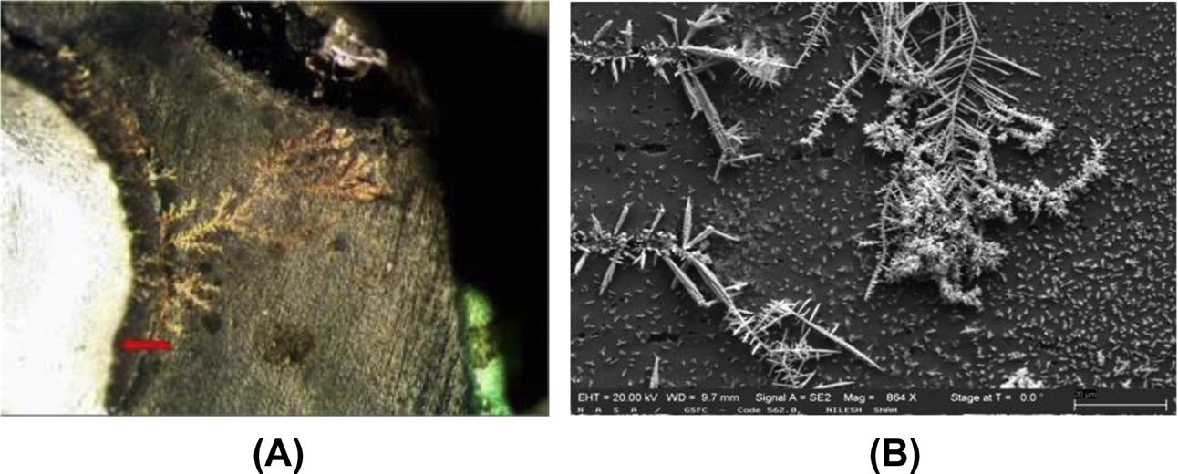
As mentioned previously, dendrites can grow on electronic parts such as printed circuit boards and capacitors (Fig. 1.11) and cause failures by short circuits [197,198,296]. Dendrites can be silver, copper, tin, lead, palladium, or a combination of metals, and their growth can be very rapid; failures have been known to occur in less than 30 minutes, but can take several months or more [198]. Corrosion of the interconnect lines can also lead to failures of the devices. The amount of contamination required for dendrites to form can be extremely small and stringent cleanliness requirements must be met (Table 1.15) [297]. Migration of metallic ions and dendrite growth has been observed at voltages as low as 0.5 V and 40% relative humidity [197].
Table 1.15
Maximum Ionic Contamination Limits for Bare Printed Circuit Boards (µg/cm2) [297]
| Ions | Non-OSP | OSP |
| Chloride (Cl−) | 0.75 | 0.75 |
| Bromide (Br−) | 1.0 | 1.0 |
| Sodium (Na+)+Potassium (K+) | 2.0 | 4.0 |
| Total inorganic | 3.8 | 5.9 |
Note: The units are in microgram of the ion per cm2 based on extraction volume and the calculated sample surface area.
OSP, organic surface protection.
This type of failure mechanism has resulted in pacemaker failures and subsequent extensive recalls for more than one manufacturer. For those electronic medical devices that operate in a high-humidity environment, such as implants, it is especially important that all ionic contaminants are removed. Ionic contamination can occur through cleaning, plating, etching, handling, fluxing, or soldering operations, as well as from airborne sources [298].
Data storage products such as disk drive components are susceptible to ionic contamination [197]. Microcontamination and subsequent corrosion of the recording head is of particular concern. The heads are composed of nickel/iron alloys that are highly susceptible to corrosive attack by anions and cations such as chloride, sulfate, and sodium. The primary mechanism is gas-phase transfer of volatile inorganic species. As in semiconductor processing, the source of the ions may be materials that are used during fabrication, ionic surfactants, aqueous rinse solutions, coatings that are used on the disk surface, packaging materials, human contact, the component assembly environment, solvents, adhesives, and lubricants.
Similar phenomena may be encountered in the manufacture of nonelectronic medical devices that are cleaned using alcohol, fluorinated, and/or chlorinated cleaning processes. Such parts include bone implants, catheters, syringes, disposable blood filters, oxygenators, dental tools, surgical tools, optical lenses, and heart valves.
7 Summary
Metallic contaminants as discrete particles and in ionic form can adversely affect the performance of electronic devices manufactured in controlled environments. The sources of the contaminants and their behavior are discussed. Metals are generally present at very low concentration levels, which makes their detection and characterization challenging. Several surface analytical techniques, such as SIMS and synchrotron-based nanoprobe X-ray fluorescence, are available with the sensitivity and resolution to access trace metals at the nanoscale. Some of the most sensitive techniques are based on electrical measurements, including carrier lifetime, electron beam–induced current microscopy, and deep-level transient spectrometry. The impacts of metallic contaminants in various applications are briefly described.
Acknowledgments
The author would like to thank the staff of the STI Library at the Johnson Space Center for help with locating obscure reference articles.
Disclaimer
Mention of commercial products in this chapter is for information only and does not imply recommendation or endorsement by The Aerospace Corporation. All trademarks, service marks, and trade names are the property of their respective owners.