
7
Pipelining, Retiming, Look-ahead Transformation and Polyphase Decomposition
7.1 Introduction
The chapter discusses pipelining, retiming and look-ahead techniques for transforming digital designs to meet the desired objectives. Broadly, signal processing systems can be classified as feed forward or feedback systems. In feed forward systems the data flows from input to output and no value in the system is fed back in a recursive loop. Finite impulse response (FIR) filters are feed forward systems and are fundamental to signal processing. Most of the signal processing algorithms such as fast Fourier transform (FFT) and discrete cosine transform (DCT) are feed forward. The timing can be improved by simply adding multiple stages of pipelining in the hardware design.
Recursive systems such as infinite impulse response (IIR) filters are also widely used in DSP. The feedback recursive algorithms are used for timing, symbol and frequency recovery in digital communication receivers. In speech processing and signal modeling, autoregressive moving average (ARMA) and autoregressive (AR) processes involve IIR systems. These systems are characterized by a difference equation . To compute an output sample, the equation directly or indirectly involves previous values of the output samples along with the current and previous values of input samples. As the previous output samples are required in the computation, adding pipeline registers to improve timing is not directly available to the designer. The chapter discusses cut-set retiming and node transfer theorem techniques for systematically adding pipelining registers in feed forward systems. These techniques are explained with examples. This chapter also discusses techniques that help in meeting timings in implementing fully dedicated architectures (FDAs) for feedback systems.
The chapter also defines some of the terms relating to digital design of feedback systems. Iteration, the iteration period, loop, loop bound and iteration period bound are explained with examples. While designing a feedback system, the designer applies mathematical transformations to bring the critical path of the design equal to the iteration period bound (IPB), which is defined as the loop bound of the critical loop of the system. The chapter then discusses the node transfer theorem and cut-set retiming techniques in reference to feedback systems. The techniques help the designer to systematically move the registers to retime the design in such a way that the transformed design has reduced critical path and ideally it is equal to the IPB.
Feedback loops pose a great challenge. It is not trivial to add pipelining and extract parallelism in these systems. The IPB limits any potential improvement in the design. The chapter highlights that if the IPB does not satisfy the sampling rate requirement even after using the fastest computational units in the design, the designer should then resort to look-ahead transformation. This transformation actually reduces the IPB at the cost of additional logic. Look-ahead transformation, by replacing the previous value of the output by its equivalent expression, adds additional registers in the loop. These additional delays reduce the IPB of the design. These delays then can be retimed to reduce the critical path delay. The chapter illustrates the effectiveness of the methodology by examples. The chapter also introduces the concept of ‘C-slow retiming’, where each register in the design is first replaced by C number of registers and these registers are then retimed for improved throughput. The design can then handle C independent streams of inputs.
The chapter also describes an application of the methodology in designing effective decimation and interpolation filters for the front end of a digital communication receiver, where the required sampling rate is much higher and any transformation that can help in reducing the IPB is very valuable.
IIR filters are traditionally not used in multi-rate decimation and interpolation applications. The recursive nature of IIR filters requires computing all intermediate values, so it cannot directly use polyphase decomposition. The chapter presents a novel methodology that makes an IIR filter use Nobel identities and effectively run at a slower clock rate in multi-rate decimation and interpolation applications.
7.2 Pipelining and Retiming
7.2.1 Basics
The advent of very large scale integration (VLSI) has reduced the cost of hardware devices. This has given more flexibility to system designers to implement computationally intensive applications in small form factors. Designers are now focusing more on performance and less on densities, as the technology is allowing more and more gates on a single piece of silicon. Higher throughout and data rates of applications are becoming the driving objectives. From the HW perspective, pipelining and parallel processing are two methods that help in achieving high throughput.
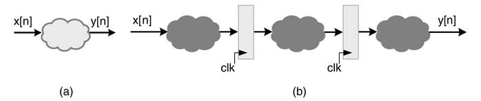
A critical path running through a combinational cloud in a feed forward system can be broken by the addition of pipeline registers. A feed forward system is one in which the current output depends only on current and previous input samples and no previous output is fed back in the system for computation of the current output. Pipeline registers only add latency. If L pipeline registers are added, the transfer function of the system is multiplied by z −L . In a feedback combinational cloud, pipeline registers cannot be simply added because insertion of delays modifies the transfer function of the system and results in change of the order of the difference equation.
Figure 7.1(a) shows a combinational cloud that is broken into three clouds by placement of two pipeline registers. This results in one-third potential reduction in the path delay of the combinational cloud. In general, in a system with L levels of pipeline stages, the number of delay elements in any path from input to output is L − 1| greater than that in the same path in the original logic. Pipelining reduces the critical path, but it increases the system latency and the output y [n ] corresponds to the previous input sample x [n − 2]. Pipelining also adds registers in all the paths, including the paths running parallel to the critical path. These extra registers add area as well as load the clock distribution. Therefore pipelining should only be added when required.
Figure 7.1 Pipeline registers are added to reduce the critical path delay of a combinational cloud. (a) Original combinational logic. (b) Design with three levels of pipelining stages with two sets of pipeline registers
Pipelining and retiming are two different aspects of digital design. In pipelining, additional registers are added that change the transfer function of the system, whereas in retiming, registers are relocated in a design to maximize the desired objective. Usually the retiming has several objectives: to reduce the critical path, reduce the number of registers, minimize power use [1, 2], increase testability [3, 4], and so on. Retiming can either move the existing registers in the design or can be followed by pipelining, where the designer places a number of registers on a cut-set line and then applies a retiming transformation to place these registers at appropriate edges to minimize the critical path while keeping all other objectives in mind.
Retiming, then, is employed to optimize a set of design objectives. These usually involve conflicting design solutions, such as maximizing performance may result in an increase in area, for example. The objectives must therefore be weighted to get the best tradeoff.
Retiming also helps in maximizing the testability of the design [4,5]. With designs based on field-programmable gate arrays (FPGAs), where registers are in abundance, retiming and pipelining transformation can optimally use this available pool of resources to maximize performance [6].
A given dataflow graph (DFG) can be retimed using cut-set or delay transfer approaches. This chapter interchangeably represents delays in the DFG with dots or registers.
7.2.2 Cut-set Retiming
Cut-set retiming is a technique to retime a dataflow graph by applying a valid cut-set line. A valid cut-set is a set of forward and backward edges in a DFG intersected by a cut-set line such that if these edges are removed from the graph, the graph becomes disjoint. The cut-set retiming involves transferring a number of delays from edges of the same direction across a cut-set line of a DFG to all edges of opposing direction across the same line. These transfers of delays do not alter the transfer function of the DFG.
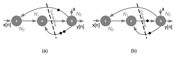
Figure 7.2(a) shows a DFG with a valid cut-set line. The line breaks the DFG into two disjoint graphs, one consisting of nodes N 0 and N 1 and the other having node N 2. The edge N 1 → N 2 is a forward cut-set edge, while N 2 → N 0 and N 2 → N 1 are backward cut-set edges. There are two delays on N 2 → N 1 and one delay on N 2 → N 0; one delay each is moved from these backward edges to the forward edge. The retimed DFG minimizing the number of registers is shown in Figure 7.2(b).
Figure 7.2 Cut-set retiming (a) DFG with cut-set line. (b) DFG after cut-set retiming
7.2.3 Retiming using the Delay Transfer Theorem
The delay transfer theorem helps in systematic shifting of registers across computational nodes. This shifting does not change the transfer function of the original DFG.
The theorem states that, without affecting the transfer function of the system, N registers can be transferred from each incoming edge of a node of a DFG to all outgoing edges of the same node, or vice versa. Figure 7.3 shows this theorem applied across a node N 0, where one register is moved from each of the outgoing edges of the DFG to all incoming edges.
Delay transfer is a special case of cut-set retiming where the cut line is placed to separate a node in a DFG. The cut-set retiming on the DFG then implements the delay transfer theorem.
7.2.4 Pipelining and Retiming in a Feed forward System
Pipelining of a feed forward system adds the appropriate number of registers in such a way that it transforms a given dataflow graph G to a pipelined one G r , such that the corresponding transfer functions H (z ) of G and Hr (z ) of Gr differ only by a pure delay z −L , where L is the number of pipeline stages added in the DFG. Adding registers followed by retiming facilitates the moving of pipeline registers in a feed forward DFG from a set of edges to others to reduce the critical path of the design.
7.2.5 Re-pipelining: Pipelining using Feed forward Cut-set
Feed forward cut-set is a technique used to add pipeline registers in a feed forward DFG. The longest (critical) path can be reduced by suitably placing pipelining registers in the architecture.
Figure 7.3 Delay transfer theorem moves one register across the node N0
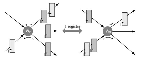
Figure 7.4 (a) Feed forward cut-set. (b) Pipeline registers added on each edge of the cut-set
Maintaining data coherency is a critical issue, but a cut-set eases the task of the designer in figuring out the coherency issues in a complex design.
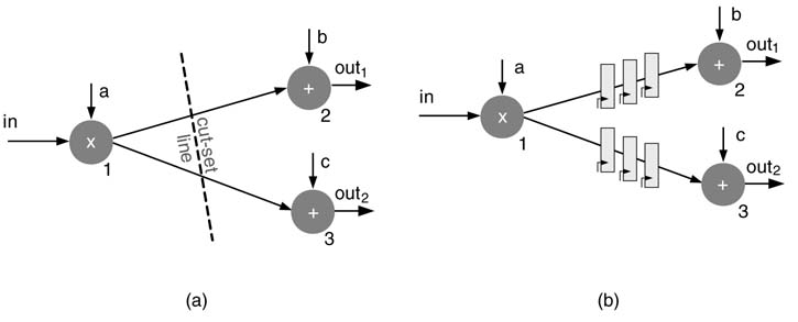
Figure 7.4 shows an example of a feed forward cut-set. If the two feed forward edges 1 → 2 and 1 → 3 are removed, the graph becomes disjoint consisting of node 1 in one graph and nodes 2 and 3 in the other graph, and two parallel paths from input to output, in → 1 → 2 → out1 and in → 1 → 3 → out2, intersect this cut-set line once.
Adding N registers to each edge of a feed forward cut-set of a DFG maintains data coherency, but the respective output is delayed by N cycles. Figure 7.4(b) shows three pipeline registers that are added on each edge of the cut-set of Figure 7.4(a). The respective outputs are delayed by three cycles.
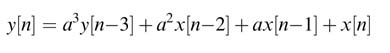
Example : The difference equation and corresponding transfer function H(z ) of a 5-coefficient FIR filter are:
(7.1a)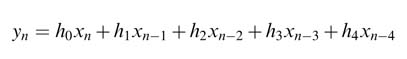
(7.1b)![]()
Assuming that general-purpose multipliers and adders are used, the critical path delay of the DFG consists of accumulated delay of the combinational cloud of one multiplier T mult, and four adders 4 × T adder. Assuming T mult is 2 time units (tu) and T adder = 1 tu, then the critical path of the design is 6 tu. It is desired to reduce this critical path by partitioning the design into two levels of pipeline stages. One feed forward cut-set can be used for appropriately adding one pipeline register in the design. Two possible cut-set lines that reduce the critical path of the design to 4 tu are shown in Figure 7.5(a). Cut-set line 2 is selected for adding pipelining as it requires the addition of only two registers. The registers are added and the pipeline design is shown in Figure 7.5(b). This reflects that the pipeline improvement is limited by the slowest pipeline stage. In this example the slowest pipeline stage consists of a multiplier and two adders.
Although the potential speed-up of two-level pipelining is two times the original design, the potential speed-up is not achieved owing to the unbalanced length of pipeline stages. The optimal speed-up requires breaking the critical path in to two exact lengths of 3 tu. This requires pipelining inside the adder, which may not be very convenient to implement or may require more registers. It is also worth mentioning that in many designs convenience is preferred over absolute optimality.
Figure 7.5 Pipelining using cut-set (a) Two candidate cut-sets in a DFG implementing a 5-coefficient FIR filter. (b) One level of pipelining registers added using cut-set 2
The pipeline design implements the following transfer function:
7.2.6 Cut-set Retiming of a Direct-form FIR Filter
Cut-set retiming can be applied to a direct-form FIR filter to get a transposed direct-form (TDF) version. The TDF is formed by first reversing the direction of addition, successively placing cut-set lines on every delay edge. Each cut-set line cuts two edges of the DFG, one in the forward and the other in the backward direction. Then retiming moves the registers from the forward edge to the backward edge. This transforms the filter from DF to TDF. This form breaks the critical path by placing a register before every addition operation. Figure 7.6 shows the process.
Example: Consider an example of fine-grain pipelining where the registers are added inside a computational unit. Figure 7.7(a) shows a 4-bit ripple carry adder (RCA). We need to reduce the critical path of the logic by half. This requires exactly dividing the combinational cloud into two stages. Figure 7.7(a) shows a cut-set line that divides the critical path into equal-delay logic, where all paths from input to output intersect the line once. Figure 7.7(b) places pipeline registers along the cut-set line. The following code implements this design:
Figure 7.6 FIR filter in direct-form transformation to a TDF structure using cut-set retiming. (a) A 4-coefficient FIR filter in DF. (b) Reversing the direction of additions in the DF and applying cut-set retiming. (c) The retimed filter in TDF
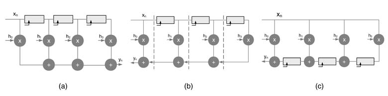
Figure 7.7 Pipelining using cut-set (a) A cut-set to pipeline a 4-bit RCA. (b) Placing pipeline registers along the cut-set line
// Module to implement a 4-bit 2-stage pipeline RCA
module pipeline_adder
(
input clk,
input [3:0] a, b,
input cin,
output reg [3:0] sum_p,
output reg cout_p);

// Pipeline registers
reg [3:2] a_preg, b_preg;
reg [1:0] s_preg;
reg c2_preg;
// Internal wires
reg [3:0] s;
reg c2;

// Combinational cloud
always @*
begin
 // Combinatinal cloud 1
 {c2, s[1:0]} = a[1:0] + b[1:0] + cin;
 // Combinational cloud 2
 {cout_p, s[3:2]} = a_preg + b_preg + c2_preg;
 // Put the output together
 sum_p = {s[3:2], s_preg};
end
// Sequential circuit: pipeline registers
always @(posedge clk)
begin
 s_preg <= s[1:0];
 a_preg <= a[3:2];
 b_preg <= b[3:2];
 c2_preg <= c2;
end
endmodule
The implementation adds two 4-bit operands a and b . The design has one set of pipeline registers that divides the combinational cloud into two equal stages. In the first stage, two LSBs of a and b are added with cin. The sum is stored in a 2-bit pipeline register s_preg. The carry out from the addition is saved in pipeline register c2_preg. In the same cycle, the combinational cloud simultaneously adds the already registered two MSBs of previous inputs a and b in 2-bit pipeline registers a_preg and b_prag with carry out from the previous cycle stored in pipeline register c2_preg. This 2-stage pipeline RCA has two full adders in the critical path, and for a set of inputs the corresponding sum and carry out is available after one clock cycle; that is, after a latency of one cycle.
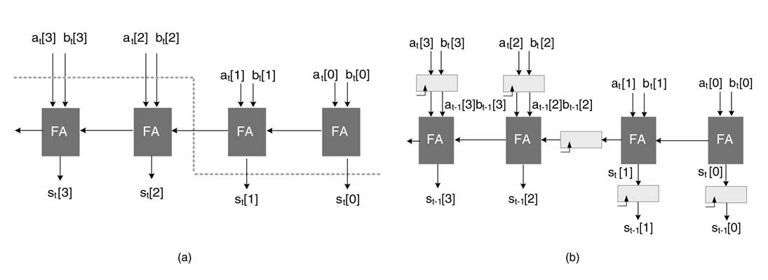
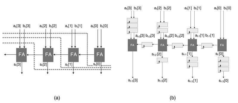
Example : Let us extend the previous example. Consider that we need to reduce the critical path to one full adder delay. This requires adding a register after the first, second and third FAs. We need to apply three cut-sets in the DFG, as shown in Figure 7.8(a). To maintain data coherency, the cut-sets ensure that all the paths from input to output have three registers. The resultant pipeline digital design is given in Figure 7.8(b). It is good practice to line up the pipeline stages or to straighten out the cut-sets lines for better visualization, as depicted in Figure 7.9.
Figure 7.8 (a) Three cut-sets for adding four pipeline stages in a 4-bit RCA. (b) Four-stage pipelined 4-bit RCA
7.2.7 Pipelining using the Delay Transfer Theorem
A convenient way to implement pipelining is to add the desired number of registers to all input edges and then, by repeated application of the node transfer theorem, systematically move the registers to break the delay of the critical path.
Figure 7.9 Following good design practice by lining up of different pipeline stages
Figure 7.10 Node transfer theorem to add one level of pipeline registers in a 4-bit RCA. (a) the original DFG. (b) Node transfer theorem applied around node FA0. (c) Node transfer theorem applied around FA1
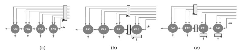
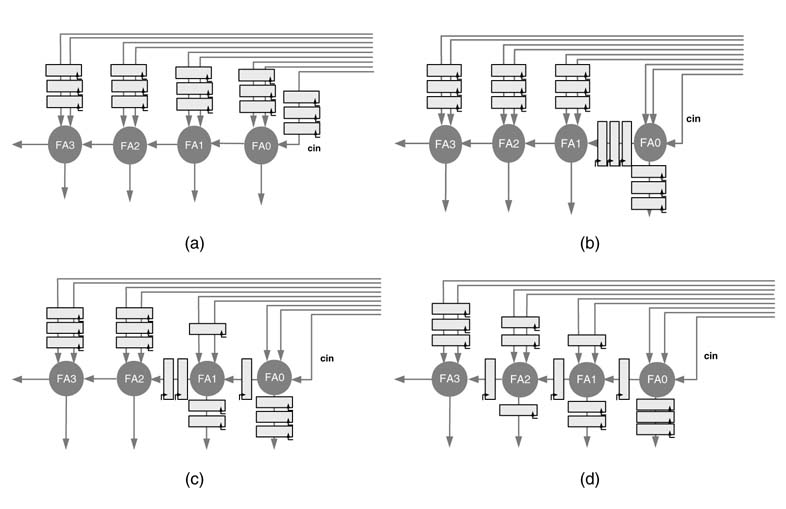
Example: Figure 7.10 shows this strategy of pipelining applied to the earlier example of adding one stage of pipeline registers in a 4-bit RCA. The objective is to break the critical path that is the carry out path from node FA1 to FA2 of the DFG. To start with, one register is added to all the input edges of the DFG, as shown in Figure 7.10(a). The node transfer theorem is applied on the FA0 node. One register each is transferred from all incoming edges of node FA0 to all outgoing edges. Figure 7.10(b) shows the resultant DFG. Now the node transfer theorem is applied on node FA1. One delay each is again transferred from all incoming edges of node FA1 to all outgoing edges. This has moved the pipeline register in the critical path of the DFG while keeping the data coherency intact. The final pipelined DFG is shown in Figure 7.10(c).
Example: This example adds three pipeline registers by applying the delay transfer theorem to a 4-bit RCA. Figure 7.11 shows the node transfer theorem applied repeatedly to place three pipeline registers at different edges. To start with, three pipeline registers are added to all input edges of the DFG, as shown in Figure 7.11(a). In the first step, three registers of first node FA0 are moved across the node to output edges, and registers at other input edges are intact. The resultant DFG is shown in Figure 7.11(b). Two registers from all input edges of node FA1 are moved to the output, as depicted in Figure 7.11(c). And finally one register from each input edge of node FA2 is moved to all output edges. This leaves three registers at input node FA3 and systematically places one register each between two consecutive FA nodes, thus breaking the critical path to one FA delay while maintaining data coherency. The final DFG is shown in Figure 7.11(d).
Figure 7.11 Adding three stages of pipeline registers by applying the node delay transfer theorem on (a) the original DFG, around (b) FA0, (c) FA1, and (d) FA2
7.2.8 Pipelining Optimized DFG
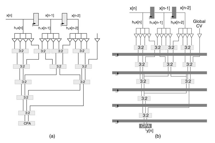
Chapter 6 explained that a general-purpose multiplier is not used for multiplication by a constant and a carry propagate adder (CPA) is avoided in the data path. An example of a direct-form FIR filter is elaborated in that chapter, where each coefficient is changed to its corresponding CSD representation. For 60–80 dB stop-band attenuation, up to four significant non-zero digits in the CSD representation of the coefficients are considered. Multiplication by a constant is then implemented by four hardwired shift operations. Each multiplier generates a maximum of four partial products (PPs). A global CV is computed which takes care of sign extension elimination logic and two’s complement logic of adding 1 to the LSB position of negative PPs. This CVisalso added in the PPs reduction tree. A Wallace reduction tree then reduces the PPs and CV in to two layers, which are added using any CPA to compute the final output.
A direct-form FIR filter with three coefficients is shown in Figure 7.12. An optimized design with CSD multiplications, PPs and CV reduction into two layers and final addition of the two layers using CPA is shown in Figure 7.13(a).
The carry propagate adder is a basic building block to finally add the last two terms that are at the output of a compression tree. The trees are extensively used in fully dedicated architecture. Adding pipeline registers in compression trees using cut-set retiming is straight forward as all the logic levels are aligned and all the paths run in parallel. A cut-set can be placed after any number of logic levels and pipeline registers can be placed at the location of the cut-set line.
The pipelined optimized design of the DF FIR filter of Figure 7.13(a) with five sets of pipeline registers in the compression tree is shown in Figure 7.13(b).
Figure 7.12 Direct-form FIR filter with three coefficients
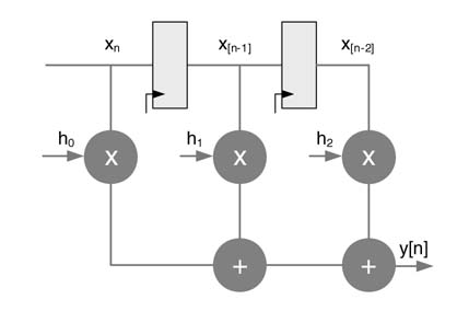
Figure 7.13 (a) Optimized implementation of 3-coefficient direct-form FIR filter. (b) Possible locations to apply cut-set pipelining to a compression tree
7.2.9 Pipelining Carry Propagate Adder
Some of the CPAs are very simple to pipeline as the logic levels in their architectures are aligned and all paths from input to output run in parallel. The conditional sum adder (CSA) is a good example where cut-set lines can be easily placed for adding pipeline registers, as shown in Figure 7.14. For other CPAs, it is not trivial to augment pipelining. An RCA, as discussed in earlier examples, requires careful handling to add pipeline registers, as does a carry generate adder.
7.2.10 Retiming Support in Synthesis Tools
Most of the synthesis tools do support automatic or semi-automatic retiming. To get assistance in pipelining, the user can also add the desired number of registers at the input or output of a feed forward design and then use automatic retiming to move these pipeline registers to optimal places. In synthesis tools, while setting timing constraints, the user can specify a synthesis option for the tool to automatically retime the registers and place them evenly in the combinational logic. The Synopsys design compiler has a balance_registers option to achieve automatic retiming [7]. This option cannot move registers in a feedback loop and some other restrictions are also applicable.
7.2.11 Mathematical Formulation of Retiming
One way of performing automatic retiming is to first translate the logic into a mathematical model [2] and then apply optimization algorithms and heuristics to optimize the objectives set in the model [4, 5]. These techniques are mainly used by synthesis tools and usually a digital designer does not get into the complications while designing the logic for large circuits. For smaller designs, the problem can be solved intuitively for effective implementation [6]. This section, therefore, only gives a description of the model and mentions some of the references that solve the models.
Figure 7.14 Pipelining a 5-bit conditional sum adder (CSA)
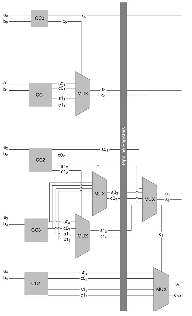
Figure 7.15 Node retiming mathematical formulation. (a) An edge eij before retiming with w (e ij ) = 1. (b) Two registers are moved-in across node i and one register is moved out across node j, for the retimed edge wr (e ij ) = 2
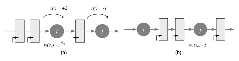
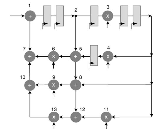
In retiming, registers are systematically moved across a node from one edge to another. Let us consider an edge between nodes i and j, and model the retiming of the edge e ij . The retiming equation is:
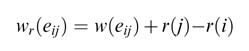
where w (e ij ) and wr (e ij ) are the number of registers on edge e ij before and after the retiming, respectively, and r (i ) and r (j ) are the number of registers moved across nodes i and j using node transfer theorem. The value of r (j ) is positive if registers are moved from outgoing edges of node j to its incoming edge e ij , and it is negative otherwise. A simple example of one edge is illustrated in Figure 7.15.
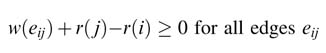
The retiming should optimize the design objective of either reducing the number of delays or minimizing the critical path. In any case, after retiming the number of registers on any edge must not be negative. This is written as a set of constraints for all edges in a mathematical modeling problem as:
Secondly, retiming should try to break the critical path between two nodes by moving the appropriate number of extra registers on the corresponding edge. The constraint is written as:
for all edges e ij in the DFG that requires C additional registers to make the nodes i and j meet timings.
The solution of the mathematical modeling problem for a DFG computes the values of all r (v ) for all the nodes v in the DFG such that the retimed DFG does not violate any constraints and still optimizes the objective function.
7.2.12 Minimizing the Number of Registers and Critical Path Delay
Retiming is also used to minimize the number of registers in the design. Figure 7.16(a) shows a graph with five registers, and (b) shows a retimed graph where registers are retimed to minimize the total number to three.
To solve the problem for large graphs, register minimization is modeled as an optimization problem. The problem is also solved using incremental algorithms where registers are recursively moved to vertices, where the number of registers is minimized and the retimed graph still satisfies the minimum clock constraint [7].
Figure 7.16 Retiming to minimize the number of registers
As the technology is shrinking, wire delays are becoming significant, so it is important for the retiming formulation to consider these too [8].
7.2.13 Retiming with Shannon Decomposition
Shannon decomposition is one transformation that can extend the scope of retiming [8, 14].It breaks down a multivariable Boolean function into a combination of two equivalent Boolean functions:
The technique identifies a late-arriving signal to a block and duplicates the logic in the block with x 0 assigning values of 0 and 1. A 2:1 multiplexer then selects the correct output from the duplicated logic. A carry select adder is a good example of Shannon decomposition. The carry path is the slowest path in a ripple carry adder. The logic in each block is duplicated with fixed carry 0 and 1and finally the correct value of the output is selected using a 2:1 multiplexer. A generalized Shannon decomposition can also hierarchically work on a multiple-input logic, as in a hierarchical carry select adder or a conditional sum adder.
Figure 7.17(a) shows a design with a slowest input x 0 to node f 0. The dependency of f 0 on x 0 is removed by Shannon decomposition that duplicates the logic in f 0 and computes it for both possible input values of x 0. A 2:1 multiplexer then selects the correct output. The registers in this Shannon decomposed design can be effectively retimed, as shown in Figure 7.17(b).
Figure 7.17 (a) Shannon decomposition removing the slowest input x 0 to f 0 and duplicating the logic in f 0 with 0 and 1 fixed input values for x 0. (b) The design is then retimed for effective timing
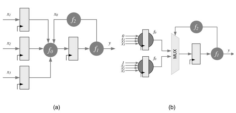
Figure 7.18 Peripheral retiming. (a) The original design. (b) Moving registers to the periphery. (c) Retiming and optimization
7.2.14 Peripheral Retiming
In peripheral retiming all the registers are moved to the periphery of the design either at the input or output of the logic. The combinational logic is then globally optimized and the registers are retimed into the optimized logic for best timing. This movement of registers on the periphery requires successive application of the node transfer theorem. In cases where some of the edges connected to the node do not have requisite registers, negative registers are added to make the movement of registers on the other edges possible. These negative registers are then removed by moving them to edges with positive retimed registers.
Figure 7.18 shows a simple case of peripheral retiming where the registers in the logic are moved to the input or output of the design. The gray circles represent combinational logic. The combinational logic is then optimized, as shown in Figure 7.18(c) where the registers are retimed for optimal placement.
7.3 Digital Design of Feedback Systems
Meeting timings in FDA-based designs for feedback systems requires creative techniques. Before elaborating on these, some basic terminology will be explained.
7.3.1 Definitions
7.3.1.1 Iteration and Iteration Period
A feedback system computes an output sample based on previous output samples and current and previous input samples. For such a system, iteration is defined as the execution of all operations in an algorithm that are required to compute one output sample. The iteration period is the time required for execution of one iteration of the algorithm.
In synchronous hard–real time systems, the system must complete execution of the current iteration before the next input sample is acquired. This imposes an upper bound on the iteration period to be less than or equal to the sampling rate of the input data.
Figure 7.19 Iteration period of first-order IIR system is equal to Tm + Ta
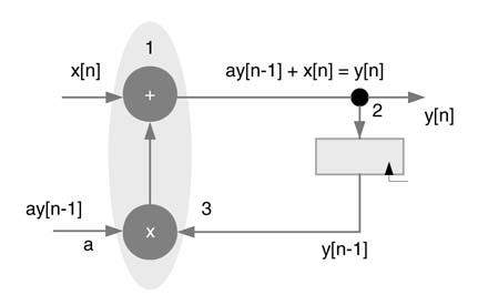
Example : Figure 7.19 shows an IIR system implementing the difference equation:
(7.3)![]()
The algorithm needs to perform one multiplication and one addition to compute an output sample in one iteration. Assume the execution times of multiplier and adder are Tm and Ta , respectively. Then the iteration period for this example is Tm + Ta . With respect to the sample period Ts of input data, these timings must satisfy the constraint:
(7.4)![]()
7.3.1.2 Loop and Loop Bound
A loop is defined as a directed path that begins and ends at the same node. In Figure 7.19 the directed path consisting of nodes 1 → 2 → 3 → 1 is a loop. The loop bound of the i th loop is defined as Ti /Di , where Ti is the loop computation time and Di is the number of delays in the loop. For the loop in Figure 7.19 the loop bound is (T m + T a)/1.
7.3.1.3 Critical Loop and Iteration Bound
A critical loop of a DFG is defined as the loop with maximum loop bound. The iteration period of a critical loop is called the iteration period bound (IPB). Mathematically it is written as:
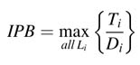
where Ti and Di are the cumulative computational time of all the nodes and the number of registers in the loop Li , respectively.
7.3.1.4 Critical Path and Critical Path Delay
The critical path of a DFG is defined as the path with the longest computation time delay among all the paths that contain zero registers. The computation time delay in the path is called the critical path delay of the DFG.
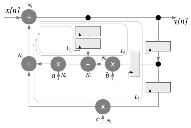
Figure 7.20 Dataflow graph with three loops. The critical loop L2 has maximum loop bound of 3.5 timing units
The critical path has great significance in digital design as the clock period is lower bounded by the delay of the critical path. Reduction in the critical path delay is usually the main objective in many designs. Techniques such as selection of high-performance computational building blocks of adders, multipliers and barrel shifters and application of retiming transformations help in reducing the critical path delay.
As mentioned earlier, for feed forward designs additional pipeline registers can further reduce the critical path. Although in feedback designs pipelining cannot be directly used, retiming can still help in reducing the critical path delay. In feedback designs, the IPB is the best time the designer can achieve using retiming without using more complex pipelining transformations. The transformations discussed in this chapter are very handy to get to the target delay specified by the IPB.
Example : The DFG shown in Figure 7.20 has three loops, L1, L2 and L3. Assume that multiplication and addition respectively take 2 and 1 time units. Then the loop bounds (LBs) of these loops are:
L2 is the critical loop as it has the maximum loop bound; that is, IPB = max{2.5, 3.5, 2} = 3.5 time units The critical path or the longest path of the DFG is N4 → N5 → N6 → N3 → N1, and the delay on the path is 7 time units. The IPB of 3.5 time units indicates that there is still significant potential to reduce the critical path using retiming, although this requires fine-grain insertion of algorithmic registers inside the computational units.
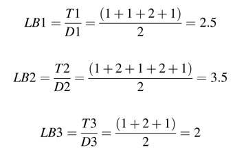
Figure 7.21 (a) Retimed DFG with critical path of 4 timing units and IPB of 3.5 timing units. (b) Fine-grain retimed DFG with critical path delay = IPB = 3.5 timing units
The designer may choose not to get to this complexity and may settle for a sub-optimal solution where the critical path is reduced but not brought down to the IPB. In the dataflow graph, recursively applying the delay transfer theorem around node N 4 and then around N 5 modifies the critical paths to N6 → N3 → N1 or N2 → N3 → N1 with critical path delay of both the paths equal to 4 time units. The DFG is shown in Figure 7.21(a).
Further reducing the critical path delay to the IPB requires a fine-grain pipelined multiplier. Each multiplier node N6 and N2 are further partitioned into two sub-nodes, N61, N62 and N21, N22, respectively, such that the computational delay of the multiplier is split as 1.5 tu and 0.5 tu, respectively, and the critical path is reduced to 3.5 tu, which is equal to the IPB. The final design is shown in Figure 7.21(b).
7.3.2 Cut-set Retiming for a Feedback System
In a feedback system, retiming described in section 7.2.2 can be employed for systematic shifting of algorithmic delays of a dataflow graph G from one set of edges to others to maximize defined design objectives such that the retimed DFG, Gr , has same transfer function. The defined objectives may be to reduce the critical path delay, the number of registers, or the power dissipation. The designer may desire to reduce a combination of these.
Example: A second-order IIR filter is shown in Figure 7.22(a). The DFG implements the difference equation:
(7.5)![]()
The critical path of the system is T m + T a, where T m and T a are the computational delays of a multiplier and adder.
Figure 7.22(a) also shows the cut-set line to move a delay for breaking the critical path of the DFG. The retimed DFG is shown in (b) with a reduced critical path equal to max{T m, T a}. The same retiming can also be achieved by applying the delay transfer theorem around the multiplier node.
Figure 7.22 Cut-set retiming (a) Dataflow graph for a second-order IIR filter. (b) Retimed DFG using cut-set retiming
Example: A third-order DF-II IIR filter is shown in Figure 7.23(a). The critical path of the DFG consists of one multiplier and three adders. The path is shown in the figure as a shaded region. Two cut-sets are applied on the DFG to implement feedback cut-set retiming. On each cut-set, one register from the cut-set line up-to-down is moved to two cut-set lines from down-to-up. The retimed DFG is shown in Figure 7.23(b) with reduced critical path of one multiplier and two adders.
7.3.3 Shannon Decomposition to Reduce the IPB
For recursive systems, the IPB defines the best timing that can be achieved by retiming. Shannon decomposition can reduce the IPB by replicating some of the critical nodes in the loop and computing them for both possible input bits and then selecting the correct answer when the output of the preceding node of the selected path is available [14].
Figure 7.24(a) shows a critical loop with one register and four combinational nodes N 0, N 1, N 2 and N 3. Assuming each node takes 2 time units for execution, the IPB of the loop is 10 tu. By taking the nodes N 2 and N 3 outside the loop and computing values for both the input 0 and 1, the IPB of the loop is now reduced to around 4 tu because only two nodes and a MUX are left in the loop, as shown in Figure 7.24(b).
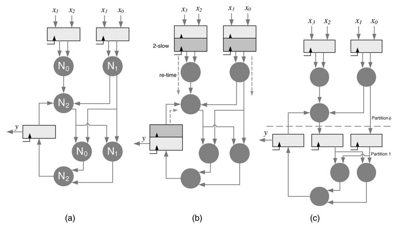
7.4 C-slow Retiming
7.4.1 Basics
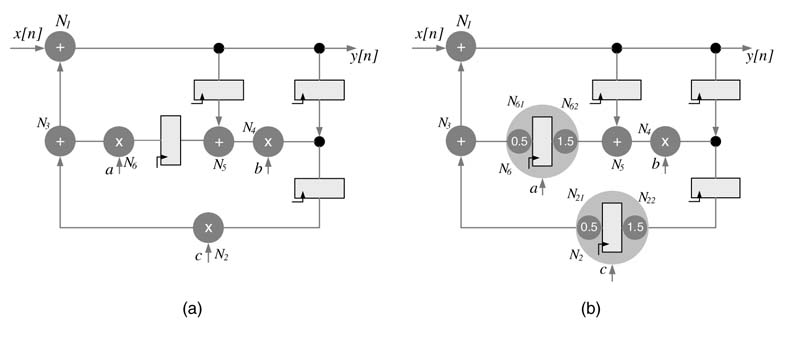
The C-slow retiming technique replaces every register in a dataflow graph with C registers. These can then be retimed to reduce the critical path delay. The resultant design now can operate on C distinct streams of data. An optimal use of C-slow design requires multiplexing of C streams of data at the input and demultiplexing of respective streams at the output.
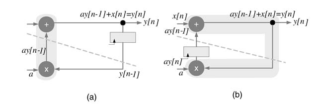
The critical path of a DFG implementing a first-order difference equation is shown in Figure 7.25(a). It is evident from Figure 7.25(b) that the critical path delay of the DFG cannot be further reduced using retiming.
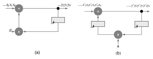
C-slow is very effective in further reducing the critical path of a feedback DFG for multiple streams of inputs. This technique works by replicating each register in the DFG with C registers and then retiming it for critical path reduction. The C-slow technique requires C streams of input data or periodically feeding C −1 nulls after every valid input to the DFG. Thus effective throughput of the design for one stream will be unaffected by the C-slow technique, but it provides an effective way to implement coarse-grain parallelism without adding any redundant combinational logic as only registers need to be replicated. The modified design of the IIR filter is shown in Figure 7.26, implementing 2-slow. The new design is fed two independent streams of input. The system runs in complete lock step processing these two streams of input x [n ] and x' [n ] and producing two corresponding streams of output y [n ] and y' [n ].
Figure 7.23 Feedback cut-set retiming on a third-order direct-form IIR filter. (a) Two cut-sets are applied on the DFG. (b) The registers are moved by applying feedback cut-set retiming
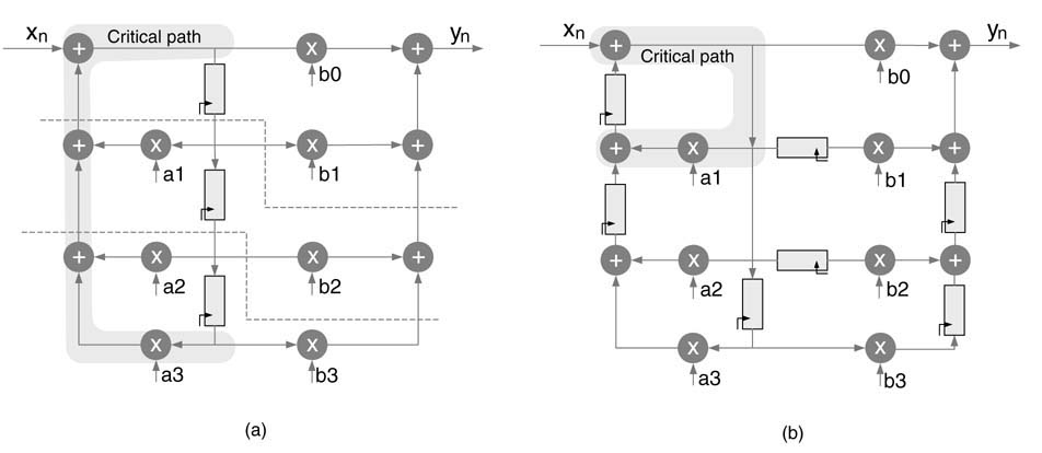
Figure 7.24 Shannon decomposition for reducing the IPB (a) Feedback loop with IPB of 8 timing units. (b) Using Shannon decomposition the IPB is reduced to around 4 timing units
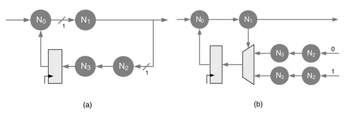
Figure 7.25 (a) Critical path delay of a first-order IIR filter. (b) Retiming with one register in a loop will result in the same critical path
Although theoretically a circuit can be C-slowed by any value of C , register setup time and clock-to-Q delay bound the number of resisters that can be added and retimed. A second limitation is in designs that may have odd places requiring many registers in retiming and thus results in a huge increase in area of the design.
Figure 7.26 C-slow retiming (a) Dataflow graph implementing a first-order difference equation. (b) A 2-slow DFG with two delays to be used in retiming
7.4.2 C-slow for Block Processing
The C-slow technique works well for block processing algorithms. C blocks from a single stream of data can be simultaneously processed by the C-slow architecture. A good example is AES encryption where a block of 128 bits is encrypted. By replicating every register in an AES architecture, with C registers the design can simultaneously encrypt C blocks of data.
7.4.3 C-slow for FPGAs and Time-multiplexed Reconfigurable Design
As FPGAs are rich in registers, the C-slow technique can effectively use these registers to process multiple streams of data. In many designs the clock frequency is fixed to a predefined value, and the C-slow technique is then very useful to meet the fixed frequency of the clock.
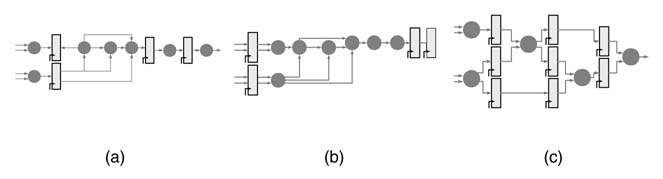
C-slow and retiming can also be used to convert a fully parallel architecture to a time-multiplexed design where C partitions can be mapped on run-time reconfigurable FPGAs. In a C-slow design, as the input is only valid at every C th clock, retiming can move the registers to divide the design into C partitions where the partitions can be optimally created to equally divide the logic into C parts. The time-multiplexed design requires less area and is also ideal for run-time reconfigurable logic.
Figure 7.27 shows the basic concept. The DFG of (a) is 2-slowed as shown in (b). Assuming all the three nodes implement some combinational logic, that is repeated twice in the design. The design is retimed to optimally place the registers while creating two equal parts. The C-slowed and retimed design is given in Figure 7.27(c). This DFG can now be mapped on time-multiplexed logic, where the data is fed into the design at one clock cycle and the results are saved in the registers. These values are input to the design that reuses the same computational nodes so C-slow reduces the area.
Figure 7.27 C-slow technique for time-multiplexed designs. (a) Original DFG with multiple nodes and few registers and large critical path. (b) Retimed DFG. (c) The DFG partitioned into two equal sets of logic where all the three nodes can be reused in a time-multiplexed design
7.4.4 C-slow for an Instruction Set Processor
C-slow can be applied to microprocessor architecture. The architecture can then run a multithreaded application where C threads are run in parallel. This arrangement does require a careful design of memories, register files, caches and other associated units of the processor.
7.5 Look-ahead Transformation for IIR filters
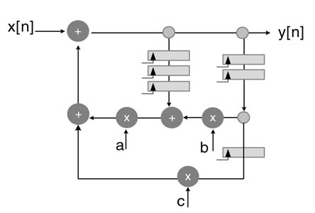
Look-ahead transformation (LAT) can be used to add pipeline registers in an IIR filter. In a simple configuration, the technique looks ahead and substitutes the expressions for previous output values in the IIR difference equation. The technique will be explained using a simple example of a difference equation implementing a first-order IIR filter:
Using this expression, y [n — 1] can be written as:
On substituting (7.7) in (7.6) we obtain:
This difference equation is implemented with two registers in the feedback loop as compared to one in the original DFG. Thus the transformation improves the IPB. These registers can be retimed for better timing in the implementation. The original filter, transformed filter and retiming of the registers are shown in Figure 7.28.
The value of y [n − 2] can be substituted again to add three registers in the feedback loop:
In general, M registers can be added by repetitive substitution of the previous value, and the generalized expression is given here:
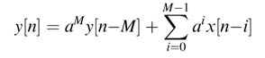
Figure 7.28 Look-ahead transformation. (a) Original first-order IIR filter. (b) Adding one register in the feedback path using look-ahead transformation. (c) Retiming the register to get better timing
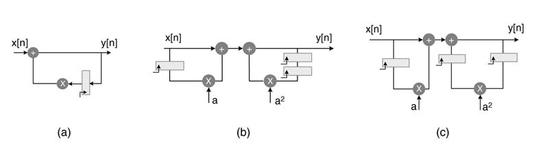
Figure 7.29 Look-ahead transformation to add M registers in the feedback path of a first-order IIR filter
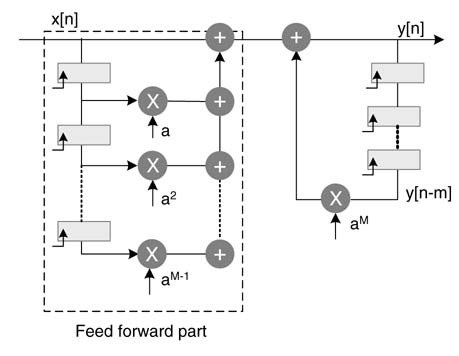
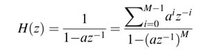
The generalized IIR filter implementing this difference equation with M registers in the feedback loop is given in Figure 7.29. This reduces the IPB of the orginal DFG by a factor of M . The difference equation implements the same transfer function H (z ):
The expression in (7.8) adds an extra M − 1 coefficients in the numerator of the transfer function of the system given in (7.9), requiring M − 1 multiplications and M − 1 additions in its implementation. These extra computations can be reduced by constraining M to be a power of 2, so that M = 2m . This makes the transfer function of (7.9) as:
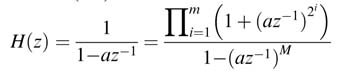
The numerator of the transfer function now can be implemented as a cascade of m FIR filters each requiring only one multiplier, where m = log2M .
Example: This example increases the IPB of a first-order IIR filter by M = 8. Applying the look-ahead transformation of (7.9), the transfer function of a first-order system with a pole at 0.9 is given as:
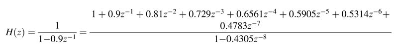
Using (7.9), this transfer function can be equivalently written as:
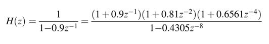
Both these expressions achieve the objective of augmenting eight registers in the feedback loop, but the transfer function using (7.9) requires three multipliers whereas the transfer function using (7.10) requires eight multipliers.
7.6 Look-ahead Transformation for Generalized IIR Filters
The look-ahead transformation techniques can be extended for pipelining any N th-order generalized IIR filter. All these general techniques multiply and divide the transfer function of the IIR filter by a polynomial that adds more registers in the critical loop or all loops of an IIR filter. These registers are then moved to reduce the IPB of the graph representing the IIR filter.
An effective technique is cluster look-ahead (CLA) transformation [9-11]. This technique adds additional registers by multiplying and dividing the transfer function by a polynomial ![]() and then solving the product in the denominator
and then solving the product in the denominator ![]() to force the first M coefficients to zero:
to force the first M coefficients to zero:
(7.11)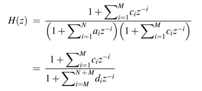
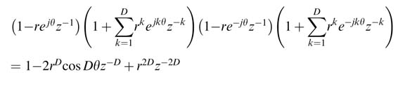
This technique does not guarantee stability of the resultant IIR filter. To solve this, scatter-edcluster look-ahead (SCA) is proposed. This adds, for every pole, an additional M − 1 poles and zeros such that the resultant transfer function is stable. The transfer function H (z ) is written as a function of z M that adds M registers for every register in the design. These registers are then moved to reduce the IPB of the dataflow graph representing the IIR filter. For conjugate poles at re ±jθ , that represents a second-order section (1 − 2r cosθz −1 + r 2z −2). Constraining M to be a power of 2, and applying SCA using expression (7.10), the transfer function corresponding to this pole pair changes to:
(7.12)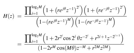
which is always stable.
There are other transformations. For example, a generalized cluster look-ahead (GCLA) does not force the first M coefficients in the expression to zero; rather it makes them equal to ±1 or some signed power of 2 [11]. This helps in achieving a stable pipelined digital IIR filter.
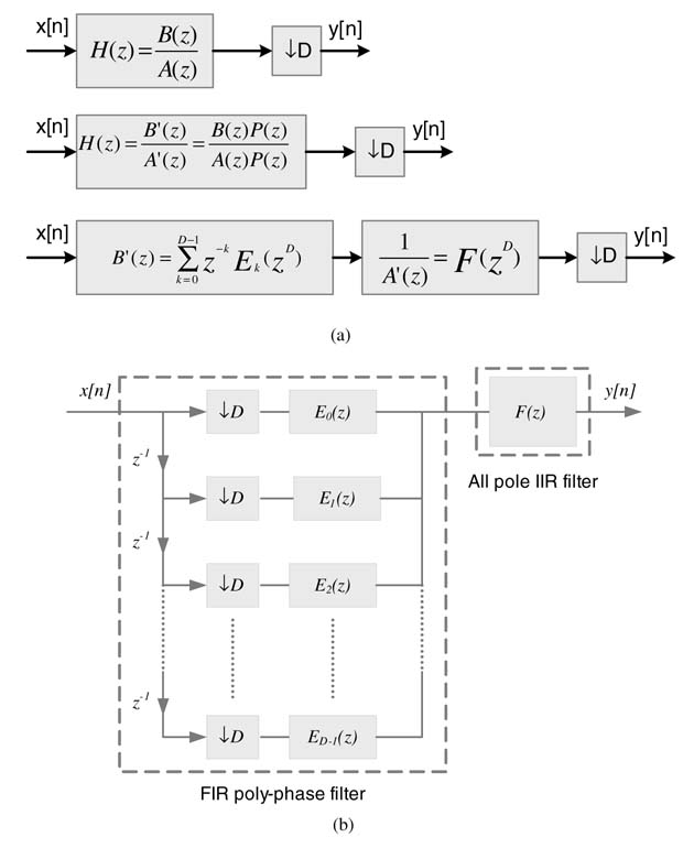
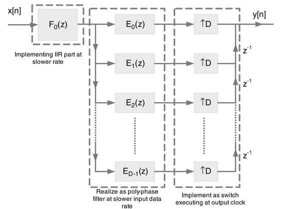
7.7 Polyphase Structure for Decimation and Interpolation Applications
The sampling rate change is very critical in many signal processing applications. The front end of a digital communication receiver is a good example. At the receiver the samples are acquired at a very high rate, and after digital mixing they go through a series of decimation filters. At the transmitter the samples are brought to a higher rate using interpolation filters and then are digitally mixed before passing the samples to a D/A converter. A polyphase decomposition of an FIR filter conveniently architects the decimation and interpolation filters to operate at slower clock rate [12].
For example, a decimation by D filters computes only the D th sample at an output clock that is slower by a factor of D than the input data rate. Similarly, for interpolation by a factor of D, theoretically the first D−1 zeros are inserted after every sample and then the signal is filtered using an interpolation FIR filter. The polyphase decomposition skips multiplication by zeros while implementing the interpolation filter.
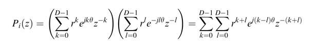
The polyphase decomposition achieves this saving by first splitting a filter with L coefficients into D sub-filters denoted by ek [n ] for k = 0… D − 1, where:
(7.13)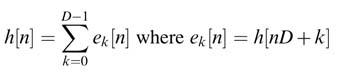
By simple substitution the desired decomposition is formulated as [13]:
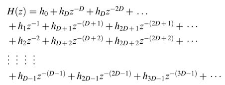
Regrouping of the expressions results in:
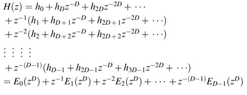
In closed form H (z ) is written as:
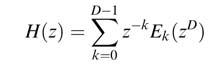
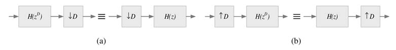
This expression is the polyphase decomposition. For decimation and interpolation applications, H (z ) is implemented as D parallel sub-systems z −k E k (z D ) realizing (7.14), as shown in Figure 7.30.
Figure 7.30 (a) Polyphase decomposition for decimation by D . (b) Application of the Noble identity for effective realization of a polyphase decomposed decimation filter. (c) Polyphase decomposition for interpolation by D . (d) Application of the Noble identity for effective realization of a polyphase decomposition interpolation filter
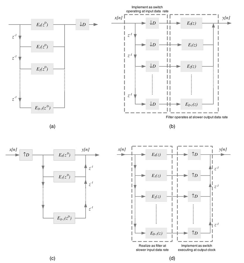
The Noble identities can be used for optimizing multi-rate structures to execute the filtering logic at a slower clock. The Noble identities for decimation and interpolation are shown in Figure 7.31.
The polyphase decomposition of a filter followed by application of the corresponding Noble identity for decimation and interpolation are shown in Figures 7.30(c) and (d).
Figure 7.31 Noble identities for (a) decimation and (b) interpolation
7.8 IIR Filter for Decimation and Interpolation
IIR filters are traditionally not used in multi-rate signal processing because they do not exploit the polyphase structure that helps in performing only needed computations at a slower clock rate. For example, while decimating a discrete signal by a factor of D , the filter only needs to compute every D th sample while skipping the intermediate computations. For a recursive filter, H (z ) cannot be simply written as a function of zD .
This section presents a novel technique for using an IIR filter in decimation and interpolation applications [15]. The technique first represents the denominator of H (z ) as a function of zD . For this the denominator is first written in product form as:
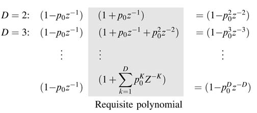
For each term in the product, the transformation converts the expression of A (z ) with N 1 real and N 2 complex conjugate pairs into a function of zD by multiplying and dividing it with requisite polynomials. For a real pole p 0, the requisite polynomial and the resultant polynomial for different values of D are given here:
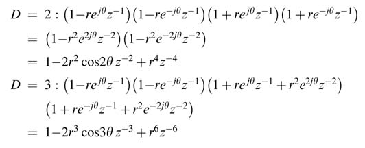
Similarly for a complex conjugate pole pair rejθ and re–jθ , the use of requisite polynomial P (z ) to transform the denominator A (z ) as a function of z–D is given here:
The generalized expression is:
This manipulation amounts to adding D −1 complex conjugate poles and their corresponding zeros. A complex conjugate zero pair contributes a 2(D − 1)th-order polynomial P (z ) with real coefficients in the numerator. A generalized close form expression of P i (z ) for a pole pair i can be computed as:
The complex exponentials in the expression can be paired for substitution as cosines using Euler’s identity. The resultant polynomial will have real coefficients.
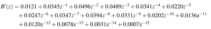
All these expressions of Pi (z )are multiplied with B (z ) to formulate a single polynomial B' (z ) in the numerator. This polynomial is decomposed in FIR polyphase filters for decimation and interpolation applications. The modified expression A' (z ) which is now a function of z–D is implemented as an all-pole IIR system. This system can be broken down into parallel form for effective realization. All the factors of the denominator can also be multiplied to write the denominator as a single polynomial where all powers of z are integer multiples of D.
The respective Noble identities can be applied for decimation and interpolation applications. The IIR filter decomposition for decimation by a factor of D is shown in Figure 7.32. An example below illustrates the decomposition for a fifth-order IIR filter.
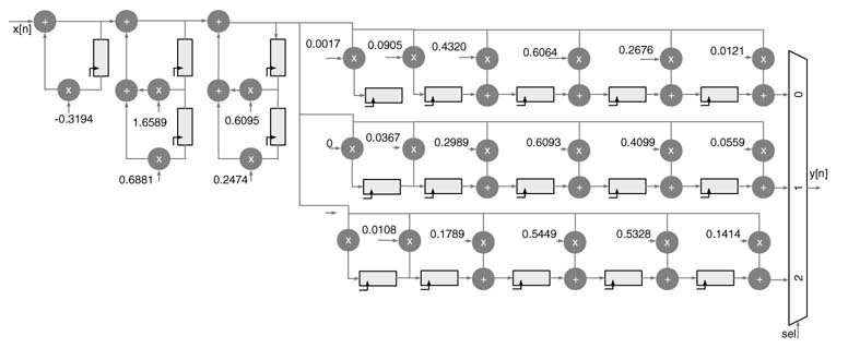
The decomposition can also be used for interpolation applications. For interpolation, the all-pole IIR component is implemented first and then its output is passed through a polyphase decomposed numerator. Both the components execute at input sample rate and output is generated at a fast running switch at output sampling rate. The design is shown in Figure 7.33.
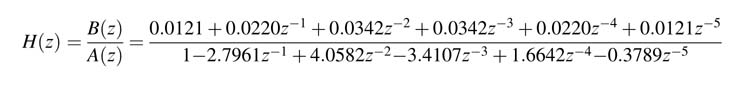
Example: Use the given fifth-order IIR filter with cut-off frequency π/ 3 in decimation and interpolation by three structures. The MATLAB® code for designing the filter with 60 dB stop-band attenuation is given here:
Fpass = 1/3; % Passband Frequency
Apass = 1; % Passband Ripple (dB)
Astop =60; % Stopband Attenuation (dB)

% Construct an FDESIGN object and call its ELLIP method.
h = fdesign.lowpass (’N,Fp,Ap,Ast’, N, Fpass, Apass,Astop);
Hd = design (h,’ellip’);
% Get the transfer function values.
[b, a] = tf (Hd);
Figure 7.32 (a) and (b) Implementation of an IIR filter for decimation applications
The transfer function is:
The denominator A (z ) is written in product form having first- and second-order polynomials with real coefficients:
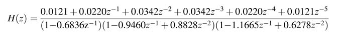
Figure 7.33Design of an IIR-based interpolation filter executing at input sample rate
By multiplying and dividing the expression with requisite factors of polynomial P (z ), the factors in the denominator are converted into a function of z −3. This computation for the denominator is given below:
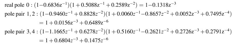
By multiplying all the above terms we get the coefficients of A' (z ) = A (z )P (z ) as a function of z −3:

The coefficients of B' (z )=B (z )P (z ) are:
The coefficients are computed using the following MATLAB® code:
p=roots (a);
% For real coefficient, generate the requisite polynomial
rP0= [1 p(5) p(5)^2];
p0= [1 –p(5)]; % the real coefficient
% Compute the new polynomial as power of z^-3
Adash0=conv(p0, rP0);% conv performs poly multiplication
% Combine pole pair to form poly with real coefficients
p1 = conv ([1 -p(1)], [1 -p(2)]);
% Generate requisite poly for first conjugate pole pair
rP1 = conv ([1 p(1) p(1)^2], [1 p(2) p(2)^2]);
% Generate polynomial in z^-3 for first conjugate pole pair
Adash1 = conv (p1, rP1);
% Repeat for second pole pair
p2 = conv ([1 -p(3)], [1 -p(4)]); %
rP2 = conv ([1 p(3) p(3)^2], [1 p(4) p(4)^2]);
Adash2 = conv (p2, rP2);
% The modified denominator in power of 3
Adash = conv (conv (Adash0, Adash1), Adash2);
% Divide numerator with the composite requisite polynomial
Bdash = conv (conv (conv(b, rP0), rP1), rP2);
% Frequency and Phase plots
figure (1)
freqz (Bdash, Adash, 1024)
figure (2)
freqz (b,a,1024);
hold off
The B' (z ) is implemented as a polyphase decimation filter, whereas 1/A '(z ) is either implemented as single-order all-pole IIR filter or converted into serial form for effective realization in fixed-point arithmetic.
Figure 7.34 shows the optimized realization of decimation by 3 using the decomposition and Noble identity where the denominator is implemented as a cascade of three serial filters. The multiplexer runs at the input data rate, whereas the FIR and IIR part of the design works at a slower clock.
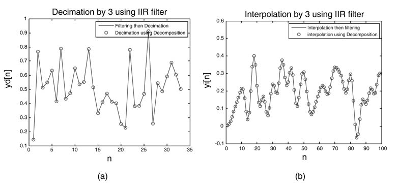
The MATLAB® code below implements the decimation using the structure given in Figure 7.34 and the result of decimation on a randomly generated data sample is shown in Figure 7.35(a). The figure shows the equivalence of this technique with the standard procedure of filtering then decimation.
Figure 7.34 Optimized implementation of a polyphase fifth-order IIR filter in decimation by a factor of 3
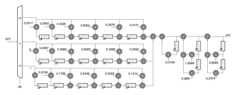
Figure 7.35 Results of equivalence for decimation and interpolation. (a) Decimation performing filtering then decimation and using the decomposed structure of Figure 7.34. (b) Interpolation by first inserting zeros then filtering and using efficient decomposition of Figure 7.34
L=99;
x=rand (1,L); % generating input samples
% Filter then decimate
y=filter (b,a,x);
yd = y (3:3:end);
% Performing decimation using decomposition technique
% Polyphase decomposition of numerator
b0=Bdash (3:3:end);
b1=Bdash (2:3:end);
b2=Bdash (1:3:end);
% Dividing input in three steams
x0=x (1:3:end);
x1=x (2:3:end);
x2=x (3:3:end);
% Filtering the streams using polyphase filters
yp0=filter (b0,1,x0);
yp1=filter (b1,1,x1);
yp2=filter (b2,1,x2);
% Adding all the samples
yp=yp0+yp1+yp2;
% Applying Nobel identity on denominator
a0=Adash0 (1:3:end);
a1=Adash1 (1:3:end);
a2=Adash2 (1:3:end);
% Filtering output of polyphase filters through IIR
% Cascaded sections
yc0=filter (1,a0,yp); % first 1st order section
yc1=filter (1,a1,yc0); % Second 2nd order section
yc = filter (1,a2,yc1); % Third 2nd order section
% Plotting the two outputs
Plot (yd);
hold on
plot (yc,’or’);
xlabel (’n’)
ylabel (’yd[n]’)
title (’Decimation by 3 using IIR filter’);
legend (’Filtering then Decimation’,’ Decimation using Decomposition’);
hold off
The novelty of the implementation is that it uses an IIR filter for decimation and only computes every third sample and runs at one-third of the sampling clock.
Example: The same technique can be used for interpolation applications. Using an IIR filter for interpolation by 3 requires a low-pass IIR filter with cut-off frequency π/3. The interpolation requires first inserting two zeros after every other sample and then passing the signal through the filter. Using a decomposition technique, the input data is first passed through the all-pole cascaded IIR filters and then the output is passed to three polyphase numerator filters. The three outputs are picked at the output of a fast running switch.
The design of an interpolator running at slower input sampling rate is given in Figure 7.36. The MATLAB® code that implements the design of this is given here. Figure 7.35(b) shows the equivalence of the efficient technique that filters a slower input sample rate with standard interpolation procedure that inserts zeros first and then filters the signal at fast output data rate.
L = 33;
x=rand (1,L); % generating input samples
% Standard technique of inserting zeros and then filtering
% Requires filter to execute at output sample rate
xi=zeros (1,3*L);
xi (1:3:end)=x;
y=filter (b,a,xi);
% Performing interpolation using decomposition technique
% Applying Nobel identity on interpolator
a0=Adash0 (1:3:end);
a1=Adash1 (1:3:end);
Figure 7.36 IIR filter decomposition interpolating a signal by a factor of 3
a2=Adash2 (1:3:end);
% Filtering input data using three cascaded IIR sections
yc0=filter (1,a0,x); % first 1st order section
yc1=filter (1,a1,yc0); % Second 2nd order section
yc = filter (1,a2,yc1); % Third 2nd order section
% Polyphase decomposition of numerator
b0=Bdash (1:3:end);
b1=Bdash (2:3:end);
b2=Bdash (3:3:end);
% Filtering the output using polyphase filters
yp0=filter (b0,1,yc);
yp1=filter (b1,1,yc);
yp2=filter (b2,1,yc);
% Switch/multiplexer working at output sampling frequency
% Generates interpolated signal at output sampling rate
y_int=zeros (1,3*L);
y_int (1:3:end)=yp0;
y_int (2:3:end)=yp1;
y_int (3:3:end)=yp2;
% Plotting the two outputs
Plot (y);
hold on
plot (y_int,’or’);
xlabel (’n’)
ylabe l (’yi[n]’)
title (’Interpolation by 3 using IIR filter’);
legend (’Interpolation then filtering’,’interpolation using Decomposition’);
hold off
Exercises
Exercise 7.1
For the DFG of Figure 7.37, assume multipliers and adders take 1 time unit, perform the following:
1. Identify all loops of the DFG and compute the critical loop bound.
2. Use a mathematical formulation to compute Wr (e 2_5), W r(e 4_5) and Wr (e 5_6) for r (5) = − 1, r (2) = −2, r (4) = 0 and r (6) = 0.
3. Draw the retimed DFG for the values computed in (2), and compute the loop bound of the retimed DFG.
Exercise 7.2
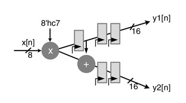
Optimally place two sets of pipeline registers in the digital design of Figure 7.38. Write RTL Verilog code of the original and pipelined design. Instantiate both designs in a stimulus for checking the correctness of the design, also observing latency due to pipelining.
Exercise 7.3
Retime the DFG of Figure 7.39. Move the two set of registers at the input to break the critical path of the digital logic. Each computational node also depicts the combinational time delay of the node in the logic.
Figure 7.37 Dataflow graph implementing an IIR filter for exercise 7.1
Exercise 7.4
Identify all the loops in the DFG of Figure 7.40, and compute the critical path delay assuming the combinational delays of the adder and the multiplier are 4 and8 tu, respectively. Compute the IPB of the graph. Apply the node transfer theorem to move the algorithmic registers for reducing the critical path and achieving the IPB.
Figure 7.38 Digital logic design for exercise 7.2
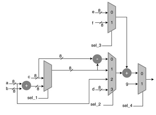
Figure 7.39 Dataflow graph for exercise 7.3
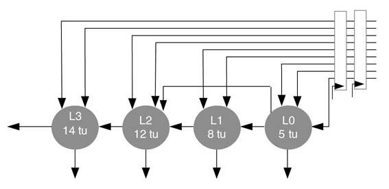
Figure 7.40 An IIR filter for exercise 7.4
Exercise 7.5
Compute the loop bound of the DFG of Figure 7.41, assuming adder and multiplier delays are 4 and 6 tu, respectively. Using look-ahead transformation adds two additional delays in the feedback loop of the design. Compute the new IPB, and optimally retime the delays to minimize the critical path of the system.
Figure 7.41 Dataflow graph for exercise 7.5
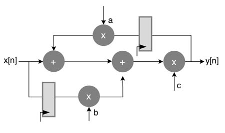
Figure 7.42 Digital design for exercise 7.6
Exercise 7.6
Design an optimal implementation of Figure 7.42. The DFG multiplies an 8-bit signed input x [n ] with a constant and adds the product in the previous product. Convert the constant to its equivalent CSD number. Generate PPs and append the adder and the CV as additional layers in the compression tree, where x [n ] is an 8-bit signed number. Appropriately retime the algorithmic registers to reduce the critical path of the compression tree. Write RTL Verilog code of the design.
Exercise 7.7
Design DF-II architecture to implement a second-order IIR filter given by the following difference equation:

Now apply C-slow retiming for C = 3, and retime the registers for reducing the critical path of the design.
1. Write RTL Verilog code of the original and 3-slow design. Convert the constants into Q1.15 format.
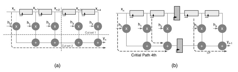
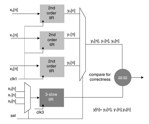
2. In the top-level module, make three instantiations of the module for the original filter and one instantiation of the module for the 3-slow filter. Generate two synchronous clocks, clk1 and clk3, where the latter is three times faster than the former. Use clk1 for the original design and clk3 for the 3-slow design. Generate three input steams of data. Input the individual streams to three instances of the original filter on clk1 and time multiplex the stream and input to C-slow design using clk3. Compare the results from all the modules for correctness of the 3-slow design.This description is shown in Figure 7.43.
Exercise 7.8
Design a time multiplex-based architecture for the C-slowed and retimed design of Figure 7.27. The design should reuse the three computational nodes by appropriately selecting inputs from multiplexers.
Exercise 7.9
Draw a block diagram of a three-stage pipeline 12-bit carry skip adder with 4-bit skip blocks.
Figure 7.43 Second-order IIR filter and 3-slow design for exercise 7.7
Exercise 7.10
Apply a look-ahead transformation to represent y [n ] as y [n − 4]. Give the IPBs for the original an transformed DFG for the following equation:
Assume both multiplier and adder take 1 time unit for execution. Also design a scattered-cluster look-ahead design for M = 4.
Exercise 7.11
Design a seventh-order IIR filter with cutoff frequency π /7 using the filter design and analysis toolbox of MATLAB®. Decompose the filter for decimation and interpolation application using the technique of Section 7.8. Code the design of interpolator and decimator in Verilog using 16-bit fixed-point signed arithmetic.
References
1. C. V. Schimpfle, S. Simon and J. A. Nossek, “Optimal placement of registers in data paths for low power design,” in Proceedings of IEEE International Symposium on Circuits and Systems, 1997, pp. 2160-2163.
2. J. Monteiro, S. Devadas and A. Ghosh, “Retiming sequential circuits for low power,” in Proceedings of IEEE International Conference on Computer-aided Design, 1993, pp. 398–402.
3. A. El-Maleh, T. E. Marchok, J. Rajski and W. Maly, “Behavior and testability preservation under the retiming transformation,” IEEE Transactions on Computer-Aided Design of Integrated Circuits and Systems, 1997, vol. 16, pp. 528-542.
4. S. Dey and S. Chakradhar, “Retiming sequential circuits to enhance testability,” in Proceedings of IEEE VLSI Test Symposium , 1994, pp. 28–33.
5. S. Krishnawamy, I. L. Markov and J. P. Hayes, “Improving testability and soft-error resilience through retiming,” in Proceedings of DAC , ACM/IEEE 2009, pp. 508–513.
6. N. Weaver, Y. Markovshiy, Y. Patel and J. Wawrzynek, “Post-placement C-slow retiming for the Xilinx Virtex FPGA,” in Proceedings of SIGDA , ACM 2003, pp. 185–194.
7. Synopsys/Xilinx. “High-density design methodology using FPGA complier,” application note, 1998.
8. D.K.Y.Tong, E.F.Y.Young, C.Chu and S.Dechu, “Wire retiming problem with net topology optimization,” IEEE Transactions on Computer-Aided Design of Integrated Circuits and Systems , 2007, vol. 26, pp. 1648–1660.
9. H. H. Loomis and B. Sinha, “High-speed recursive digital filter realization,” Circuits, Systems Signal Processing , 1984, vol. 3, pp. 267–294.
10. K.K. Parhi andD.G.Messerschmitt, “Pipeline interleaving and parallelisminrecursive digital filters.-Pts Iand II,” IEEE Transactions on Acoustics, Speech and Signal Processing , 1989, vol. 37, pp. 1099–1135.
11. Z. Jiang and A. N. Willson, “Design and implementation of efficient pipelined IIR digital filters,” IEEE Transactions on Signal Processing , 1995, vol. 43, pp. 579–590.
12. F. J. Harris, C. Dick and M. Rice, “Digital receivers and transmitters using polyphase filter banks for wireless communications,” IEEE Transactions on Microwave Theory and Technology , 2003, vol. 51, pp. 1395–1412.
13. A.V. Oppenheim and R. W. Schafer, Discrete-time Signal Processing , 3rd edn, 2009, Prentice-Hall.
14. C.Soviani, O. Tardieu, and S. A. Edwards, ‘‘Optimizing Sequential Cycles Through Shannon Decomposition and Retiming’’, IEEE Transactions on Computer-Aided Design of Integrated Circuits and Systems , vol. 26, no. 3, March 2007.
15. S. A. Khan, ‘‘Effective IIR filter architectures for decimation and interpolation applications’’, Technical Report CASE May 2010.