
10
Micro-programmed State Machines
10.1 Introduction
In time-shared architecture, computational units are shared to execute different operations of the algorithm in different cycles. As described in Chapter 9, time-shared architecture consists of a datapath and a control unit. In each clock cycle the control unit generates appropriate control signals for the datapath. In hardwired state machine-based designs, the controller is implemented as a Mealy or Moore finite state machine (FSM). However, in many applications the algorithms are so complex that a hardwired FSM design is not feasible. In other applications, either several algorithms need to be implemented on the same datapath or the designer wants to keep the flexibility of modifying the controller without repeating the entire design cycle, so a flexible controller is implemented to use the same datapath for different algorithms. The controller is made programmable [1].
This chapter describes the design of micro-programmed state machines with various capabilities and options. A methodology for converting a hardwired state machine to a micro-programmed implementation is introduced. The chapter gives an equivalent micro-programmed implementations of the examples already covered in previous chapters. The chapter then extends the implementation by describing a design of FIFO and LIFO queues on the same datapath running micro-programs.
The chapter then switches to implementation of DSP algorithms on time-shared architecture. Analysis of a few algorithms shows that in many cases a simple counter-based micro-programmed state machine can be used to implement a controller. The memory contains all the control signals to be generated in a sequence, whereas the counter keeps computing the address of the next micro-code stored in memory. In applications where decision-based execution of operations is required, this elementary counter-based state machine is augmented with decision support capability. The execution is based on a few condition lines coming either from the datapath or externally from some other blocks. These conditions are used in conditional jump instructions. Further to this, the counter in the state machine can be replaced by a program counter (PC) register, which in normal execution adds a fixed offset to its content to get the address of the next instruction. The chapter then describes cases where a program, instead of executing the next micro-code, needs to take a jump to execute a sequence of instructions store data different location in the program memory. This requires subroutine support in the state machine.
This chapter also covers the design of nested subroutine support whereby a subroutine can be called inside another subroutine. This is of special interest in image and signal processing applications, giving the capability to repeatedly execute a block of instructions a number of times without any loop maintenance overhead.
The chapter finishes with a complete example of a design that uses all the features of a micro-programmed state machine.
10.2 Micro-programmed Controller
10.2.1 Basics
The first step in designing a programmable architecture is to define an instruction set. This is defined such that a micro-program based on the instructions implements the target application effectively. The datapath and a controller are then designed to execute the instruction set. The controller in this case is micro-program memory-based. This design is required to have flexibility not only to implement the application but also to support any likely modifications or upgrading of the algorithm [2].
An FSM has two components, combinational and sequential. The sequential component consists of a state register that stores the current state of the FSM. In the Mealy machine implementation, combinational logic computes outputs and the next state from inputs and the current state. In a hardwired FSM this combinational logic cannot be programmed to change its functionality. In a micro-programmable state machine the combinational logic is replaced by a sequence of control signals that are stored in program memory (PM), as shown in Figure 10.1. The PM may be a read only (ROM) or random-access (RAM).
A micro-programmed state machine stores the entire output sequence of control signals along with the associated next state in program memory. The address of the contents in the memory is determined by the current state and input to the FSM.
Assume a hypothetical example of a hardwired FSM design that has two 1-bit inputs, six 1-bit outputs and a 6-bit state register. Now, to add flexibility in the controller, the designer wishes to replace the hardwired FSM. The designer evaluates all possible state transitions based on inputs and the current state and tabulates the outputs and next states as micro-coding for PM. These values are placed in the PM such that the inputs and the current state provide the index or address to the PM. Figure 10.2 shows the design of this micro-programmed state machine.
Figure 10.1 Micro-programmed state machine design showing program memory and state register
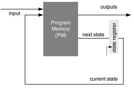
Figure 10.2 Hypothetical micro-programmed state machine design
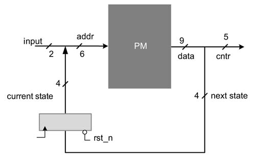
Mapping this configuration on the example under consideration makes the micro-program PM address bus 6 bits wide and its data bus 9 bits wide. The 2-bit input constitutes the two least significant bits (LSBs) of the address bus, addr[1:0], whereas the current state forms the rest of the four most significant bits (MSBs) of the address bus, addr[5:2]. The contents of the memory are worked out from the ASM chart to produce desired output control signals and the next state for the state machine. The ASM chart for this example is not given here as the focus is more on discussing the main components of the design.
The five LSBs of the data bus, data[4:0], are allocated for the outputs cntr[4:0], and the four MSBs of the data bus, data[8:5], are used for the next state. At every positive edge of the clock the state register latches the value of the next state to the state register. This value becomes the current state in the next clock cycle.
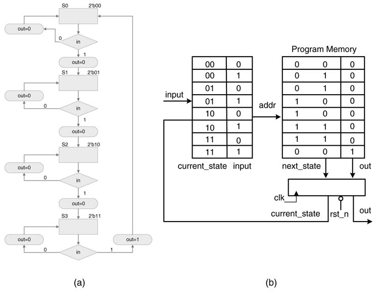
Example: This example designs a state machine that implements the four 1s detection problem of Chapter 9, where the same was realized as hardwired Mealy and Moore state machines.
The ASM chart for the Mealy machine implementation is given in Figure 10.3.(a). This design has 1-bit input and 1-bit output and its state register is 2 bits wide. The PM-based micro-coded design requires a 3-bit address bus and a 3-bit data bus. The address bus requires the PM to be 23 = 8 bits deep. The contents of the memory can be easily filled following the ASM chart of Figure 10.3(a). The address 3′b000 defines the current state of S0 and the input 1′b0. The next state and output for this current state and input can be read from the ASM chart. The chart shows that in state S0, if the input is 0 then the output is also 0 and the next state remains S0. Therefore the content of memory at address 3′b000 is filled with 3′b000. The LSB of the data bus is output and the rest of the 2 bits defines the next state. Similarly the next address of 3′b001 defines the current state to be S0 and the input as 1. The ASM chart shows that in state S0, if input is 1 the next state is S1 and output is 0. The contents of the PM at address 3′b001 is filled with 3′b010. Similarly for each address, the current state and the input is parsed and the values of next state and output are read from the ASM chart. The contents of PM are accordingly filled. The PM for the four 1s detected problem is given in Figure 10.3(b) and the RTL Verilog of the design is listed here:
Figure 10.3 Moving from hardwired to micro-coded design. (a) ASM chart for four1sdetected problem of Figure 9.9 in Chapter 9. (b) Equivalent micro-programmed state machine design
// Module to implement micro-coded Mealy machine
module fsm_mic_mealy
(
input clk, // System clock
input rst_n, // System reset
input data_in, // 1-bit input stream
output four_ones_det // To indicate four 1s are detected
);
// Internal variables
reg [1:0] current_state; // 2-bit current state register
wire [1:0] next_state; // Next state output of the ROM
wire [2:0] addr_in; // 3-bit address for the ROM
// This micro-programmed ROM contains information of state transitions
mic_prog_rom mic_prog_rom_inst
(
.addr_in (addr_in),
.next_state (next_state),
.four_ones_det (four_ones_det)
);
// ROM address
assign addr_in = {current_state, data_in};
// Current state register
always @ (posedge clk or negedge rst_n)
begin : current_state_bl
 if (!rst_n)
 current_state <= #1 2b0; // One-hot encoded
 else
 current_state <= #1 next_state; // Next state from the ROM
end
endmodule

// Module to implement PM for state transition information
module mic_prog_rom
(
input [2:0] addr_in, // Address of the ROM
output reg [1:0] next_state, // Next state output
output reg four_ones_det // Detection of signal output
);

always @ (addr_in)
begin : ROM_bl
 case(addr_in)
 3b00_0 :
 {next_state, four_ones_det} = {4b00, 1b0};
 3b00_1 :
 {next_state, four_ones_det} = {4b01, 1b0};
 3b01_0 :
 {next_state, four_ones_det} = {4b01, 1b0};
 3b01_1 :
 {next_state, four_ones_det} = {4b10, 1b0};
 3b10_0 :
 {next_state, four_ones_det} = {4b10, 1b0};
 3b10_1 :
 {next_state, four_ones_det} = {4b11, 1b0};
 3b11_0 :
 {next_state, four_ones_det} = {4b11, 1b0};
 3b11_1 :
 {next_state, four_ones_det} = {4b00, 1b1};
 endcase
End
endmodule
Micro-programmed state machine implementation provides flexibility as changes in the behavior of the state machine can be simply implemented by loading a new micro-code in the memory. Assume the designer intends to generate a 1 and transition to state S3 when the current state is S2 and the input is 1. This can be easily accomplished by changing the memory contents of PM at location 3′b101 to 3′b111.
10.2.2 Moore Micro-programmed State Machines
For Moore machine implementation the micro-program memory is split into two parts, so the combinational logic-I and logic-II are replaced by PM-I and PM-II. The input and the current state constitute the address for PM-I. The memory contents of PM-I are filled to appropriately generate the next state according to the ASM chart. The width of PM-I is equal to the size of the current state register, whereas its depth is 23 = 8 (3 is the size of input plus current state). Only the current state acts as the address for PM-II. The contents of PM-II generate output signals for the datapath.
Figure 10.4 (a) Moore machine ASM chart for the four 1s detected problem. (b) Micro-program state machine design for the Moore machine
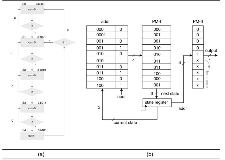
A micro-programmed state machine design for the four 1s detected problem is shown in Figure 10.4. One bit of the input and three bits of the current state constitute the 4-bit address bus for PM-I. The contents of the memory are micro-programmed to generate the next state following the ASM chart. Only three bits of the current state form the address bus of PM-II. The contents of PM-II are filled to generate a control signal in accordance with the ASM chart.
10.2.3 Example: LIFO and FIFO
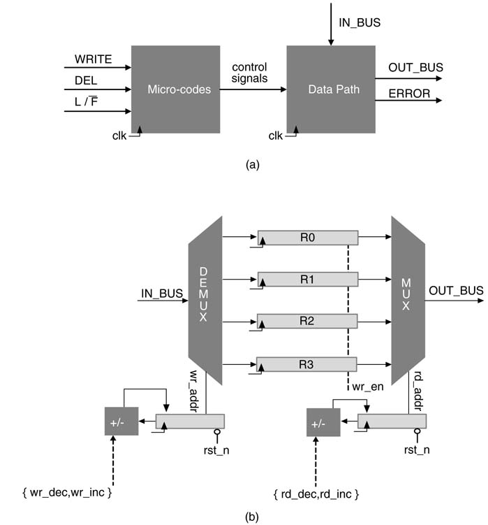
This example illustrates a datapath that consists of four registers and associated logic to be used as LIFO (last-in first-out) or FIFO (first-in first-out). In both cases the user invokes different micro-codes consisting of a sequence of control signals to get the desired functionality. The top-level design consisting of datapath and controller is shown in Figure 10.5.(a).
Out of a number of design options, a representative datapath is shown in Figure 10.5.(b). The write address register wr_addr_reg is used for selecting the register for the write operation. A wr_en increments this register and the value on the INBUS is latched into the register selected by the wr_addr value. Similarly the value pointed by read address register rd_addr_reg is always available on the OUTBUS. This value is the last or the first value input to a LIFO or a FIFO mode, respectively. ADEL operation increments the register rd_add_reg. The control signal rd_inc is asserted to increment the value on a valid DEL request. The micro-codes for the controller are listed in Table 10.1. The current states are S0, S1 and S2, and next states are depicted by NS0, NS1 and NS2.
Figure 10.5 (a) Block diagram for datapath design to support both LIFO and FIFO functionality. (b) Representative datapath to implement both LIFO and FIFO functionality for micro-coded design
10.3 Counter-based State Machines
10.3.1 Basics
Many controller designs do not depend on the external inputs. The FSMs of these designs generate a sequence of control signals without any consideration of inputs. The sequence is stored serially in the program memory. To read a value, the design only needs to generate addresses to the PM in a sequence starting from 0 and ending at the address in the PM that stores the last set of control signals. The addresses can be easily generated with a counter. The counter thus acts as the state register where the next state is automatically generated with an increment. The architecture results in a reduction in PM size as the memory does not store the next state and only stores the control signals. The machine is reset to start from address 0 and then in every clock cycle it reads a micro-code from the memory. The counter is incremented in every cycle, generating the next state that is the address of the next micro-code in PM.
Table 10.1 Micro-codes implementing FIFO and LIFO
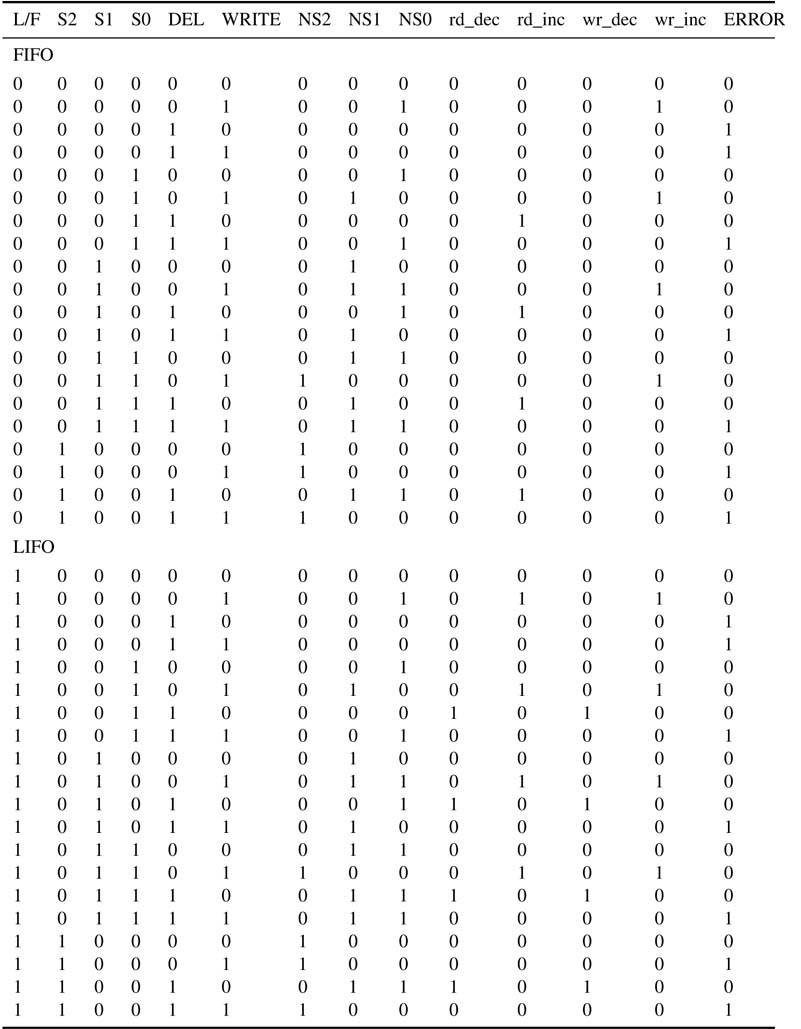
Figure 10.6 Counter-based micro-program state machine implementation
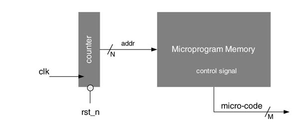
Figure 10.6 shows an example. An N-bit resetable counter is used to generate addresses for the program memory in a sequence from 0 to 2N– 1. The PM is M bits wide and 2N– 1 deep, and stores the sequence of signals for controlling the datapath. The counter increments the address to memory in every clock cycle, and the control signals in the sequence are output on the data bus. For executing desired operations, the output signals are appropriately connected to different blocks in the datapath.
10.3.2 Loadable Counter-based State Machine
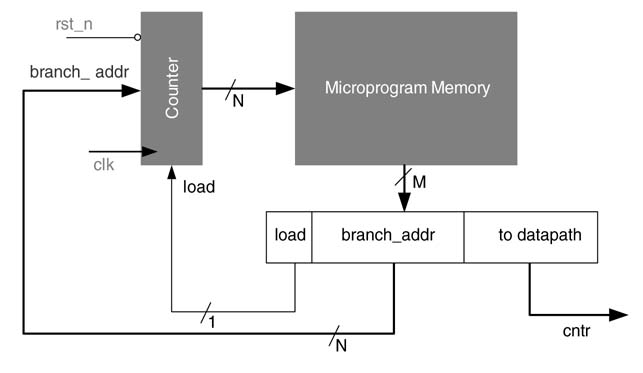
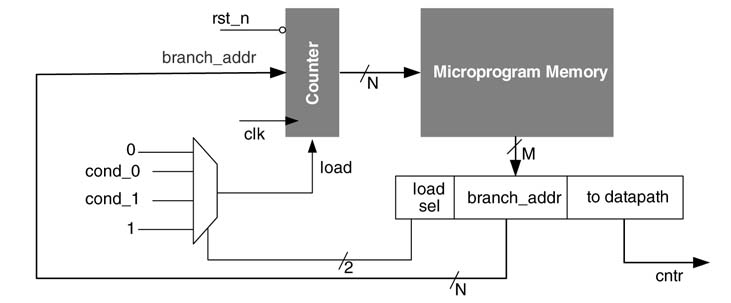
As described above, a simple counter-based micro-programmed state machine can only generate control signals in a sequence. However, many algorithms once mapped on time-shared architecture may also require out-of-sequence execution, whereby the controller is capable of jumping to start generating control signals from a new address in the PM. This flexibility is achieved by incorporating the address to be branched as part of the micro-code and a loadable counter latches this value when the load signal is asserted. This is called ‘unconditional branching’. Figure 10.7 shows the design of a micro-programmed state machine with a loadable counter.
Figure 10.7 Counter-based controller with unconditional branching
10.3.3 Counter-based FSM with Conditional Branching
The control inputs usually come from the datapath status-and-control register (SCR). On the basis of execution of some micro-code, the ALU (arithmetic logic unit) in the datapath sets corresponding bits of the SCR. Examples of control bits are zero and positive status bits in the SCR. These bits are set if the result of a previous ALU instruction is zero or positive. These two status bits allow selection of conditional branching. In this case the state machine will check whether the input control signal from the datapath is TRUE or FALSE. The controller will load the branch address in the counter if the conditional input is TRUE; otherwise the controller will keep generating sequential control signals from program memory. The micro-code may look like this:
if(zero_flag) jump to label0
or
if(positive_flag) jump to label1
where zero_flag and postivie_flag are the zero and positive status bits of the SCR, and label0 and label1 are branch addresses. The controller jumps to this new location and reads the micro-code starting from this address if the conditional input is TRUE.
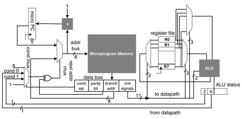
The datapath usually has one or more register files. The data from memory is loaded in the register files. The ALU operates on the data from the register file and stores the result in memory or in the register file. A representative block diagram of a datapath and controller is shown in Figure 10.8.
The conditional bits can also directly come from the datapath and be used in the same cycle by the controller. In this case the conditional micro-code may look like this:
if(r1==r2) jump to label1
Figure 10.8 Representative design of controller, datapath with register file, data memory and SCR
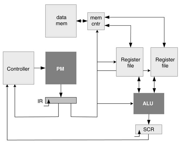
Figure 10.9 Micro-programmed state machine with conditional branch support
The datapath subtracts the value in register r1 from r2, and if the result of this subtraction is 0 the state machine executes the micro-code starting from label1.
To provision the branching capabilities, a conditional multiplexer is added in the controller as shown in Figure 10.9. Two load_sel bits in the micro-code select one of the four inputs to the conditional MUX. If load_sel is set to 2′b00, the conditional MUX selects 0 as the output to the load signal to the counter. With the load signal set to FALSE, the counter retains its normal execution and sequentially generates the next address for the PM. If, however, the programmer sets load_sel to 2′b11, the conditional MUX selects 1 as the output to the load signal to the counter. The counter then loads the branch address and starts reading micro-code from this address. This is equivalent to unconditional branch support earlier. Similarly, if load_sel is set to 2′b01 or 2′b10, the MUX selects, respectively, one of the condition bits cond_0 or cond_1 for the load signal of the counter. If the selected condition bit is set to TRUE, the counter loads the branch_addr; otherwise it keeps its sequential execution.
Table 10.2 summarizes the options added to the counter-based state machine by incorporating a conditional multiplexer in the design.
10.3.4 Register-based Controllers
In many micro-programmed FSM designs an adder and a register replace the counter in the architecture. This register is called a micro-program counter (PC) register. The adder adds 1 to the content of the PC register to generate the address of the next micro-code in the micro-program memory.
Table 10.2 Summary of operations a micro-coded state machine performs based on load_sel and conditional inputs
| load_sel | Load |
| 2′b00 | FALSE (normal execution: never load branch address) |
| 2′b01 | cond_0 (load branch address if cond_0 is TRUE) |
| 2′b10 | cond_1 (load branch address if cond_1 is TRUE) |
| 2′b11 | TRUE (unconditional jump: always load branch address) |
Figure 10.10 Micro-PC-based design
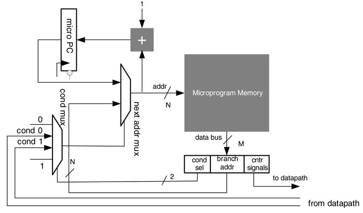
Figure 10.10 shows an example. The next_addr_mux selects the address to the micro-program memory. For normal execution, cond_mux selects 0. The output from cond_mux is used as the selected line to next_addr_mux. Then, mirco_PC and branch_addr are two inputs to next_addr_mux. A zero at the selected line to this multiplexer selects the value of micro_PC and a 1 selects the branch_addr to addr_bus. The addr_bus is also input to the adder that adds 1 to the content of addr_bus. This value is latched in micro_PC in the next clock cycle.
10.3.5Register-based Machine with Parity Field
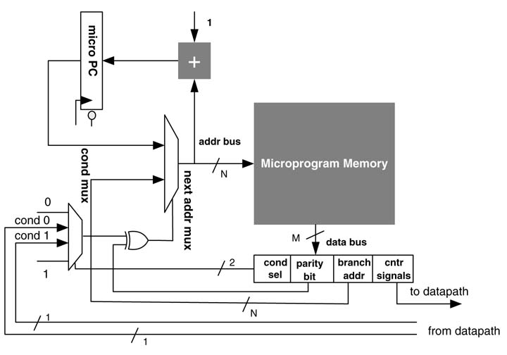
A parity bit can be added in the micro-code to expand the conditional branching capability of the state machine of Figure 10.10. The parity bit enables the controller to branch on both TRUE and FALSE states of conditional inputs. If the parity bit is set, the EXOR gate inverts the selected condition of cond_mux, whereas if the parity bit is not set the selected condition then selects the next_addr to the micro-program memory.
A controller with a parity field in the micro-code is depicted in Figure 10.11. The parity bit is set to 0 with the following micro-code:
if (cond_0) jump to label
The parity bit is set to 1 with the following micro-code:
if(!cond_0) jump to label
10.3.6Example to Illustrate Complete Functionality
This example (see Figure 10.12) illustrates the complete functionality of a design based on a micro-programmed state machine. The datapath executes operations based on the control signals generated by the controller. These control signals are stored in the PM of the controller. The datapath has one register file. The register file stores operands. (In most designs these operands are loaded from memory. For simplicity this functionality is not included in the example.)
Figure 10.11 Register-based controller with a parity field in the micro-code
The register file has two read ports and one write port. For eight registers in the register file, 3 bits of the control signal are used to select a register to be read from each read port, and 3 bits of the control signal are used to select a register to be written by an ALU micro-code. The datapath based on the result of the executed micro-code updates the Z and N bits of the ALU status register. The Z bit is set if the result of an ALU micro-code is 0, while a negative value of the ALU result sets the N bit of the status register. These two bits are used as cond_0 and cond_1 bits of the controller. The design supports a program that uses the following set of micro-codes:
Figure 10.12 Different fields in the micro-code of the programmable state machine design of the text example. (a) Non-overlapping fields. (b) Overlapping fields to reduce the width of the PM
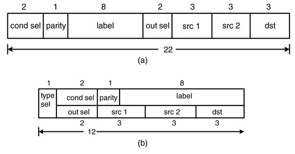
Figure 10.13 Example to illustrate complete working of a micro-programmed state machine design
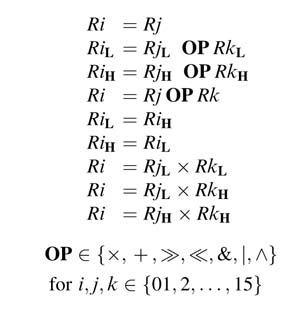
Ri = Rj op Rk, for i, j, k= 0, 1, 2,…,7 and op is any one of the four supported ALU
operations of +, -, AND, OR, an example micro code is R2 = R3 + R5
if (N) jump label
if (!N) jump label
if (Z) jump label
if (!Z) jump label
jump label
These micro-codes control the datapath and also support the conditional and unconditional branch instruction. For accessing three of eight registers Ri, Rj and Rk, three sets of 3 bits are required. Similarly, to select one of the outputs from four ALU operations, 2 bits are needed. This makes the total number of bits to the datapath11. The label depends on the size of the PM: to address 256 words, 8 bits are required. To support conditional instructions, 2 bits are required for conditional multiplexer selection and 1 bit for the parity. These bits can be linearly placed or can share fields for branch and normal instructions. The sharing of fields saves on instruction width at the cost of adding a little complexity in decoding the instruction. In cases of sharing, 1 bit is required to distinguish between branching and normal ALU instructions.
The datapath and the micro-programmed state machine are shown in Figure 10.12. The two options for fields of the micro-code are shown in Figure 10.13. The machine uses the linear option for coding the micro-codes.
10.4 Subroutine Support
In many applications it is desired to repeat a set of micro-code instructions from different places in the micro-program. This can be effectively achieved by adding subroutine capability. Those microcode instructions that are to be repeated can be placed in a subroutine that is called from any location in the program memory.
Figure 10.14 Micro-programmed state machine with subroutine support
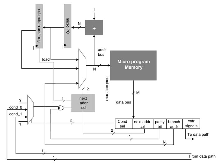
The state machine, after executing the sequence of operations in the subroutine, needs to return to the next micro-code instruction. This requires storing of a return address in a register. This is easily accomplished in the cycle in which the call to the subroutine is made; micro_PC has the address of the next instruction, so this address is the subroutine return address. The state machine saves the contents of micro_PC in a special register called the subroutine return address (SRA) register. Figure 10.14 shows an example.
While executing the micro-code for the subroutine call, the next-address select logic generates a write enable signal to the SRA register. For returning from the subroutine, a return micro-code is added in the instruction-set of the state machine. While executing the return micro-code, the next-address select logic directs the next address multiplexer to select the address stored in the SRA register. The micro-code at the return address is read for execution. In the next clock cycle the micro-PC stores an incremented value of the next address, and a sequence of micro-codes is executed from there on.
10.5 Nested Subroutine Support
There are design instances where a call to a subroutine is made from an already called subroutine, as shown in Figure 10.15. This necessitates saving more than one return address in a last-in first-out (LIFO) stack. The depth of the stack depends on the level of nesting to be supported. A stack management controller maintains the top and bottom of the stack. To support J levels of nesting the LIFO stack needs J registers.
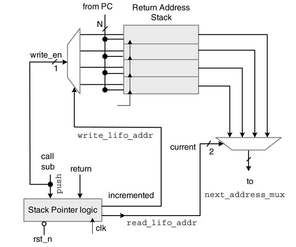
There are several options for designing the subroutine return address stack. A simple design of a LIFO is shown in Figure 10.16. Four registers are placed in the LIFO to support four nested subroutine calls. This LIFO is designed for a micro-program memory with a 10-bit address bus.
Figure 10.15 Micro-program state machine with nested subroutine support
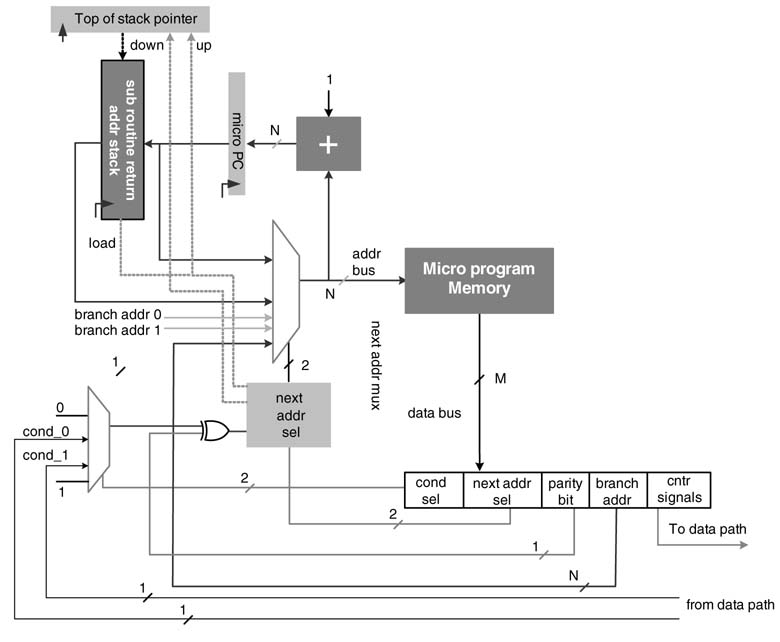
A stack pointer register points to the last address in the LIFO with read_lifo_addr control signal. The signal is input to a 4:1 MUX and selects the last address stored in the LIFO and feeds it as one of the inputs to next_address_mux. To store the next return address for a nested subroutine call, write_lifo_addr control signal points to the next location in the LIFO. On a subroutine call, the push signal is asserted which enables the decoder, and the value in the PC is stored in the register pointed by write_lifo_addr and the value stored in the stack pointer is incremented by 1. On a return to subroutine call, the value stored in the stack pointer register is decremented by 1.
The design can be modified to check error conditions and to assert an error flag if a return from a subroutine without any call, or more than four nested subroutine calls, are made.
10.6 Nested Loop Support
Signal processing applications in general, and image and video processing applications in particular, require nested loop support. It is critical for the designer to minimize the loop maintenance overhead. This is associated with decrementing the loop counter, and checking where the loop does not expire and the program flow needs to be branched back to the loop start address. A micro-programmed state machine can be equipped to support the loop overhead in hardware. This zero-overhead loop support is especially of interest to multimedia controller designs that requires execution of regular repetitive loops [3].
Figure 10.16 Subroutine return address stack
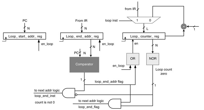
A representative instruction for a loop can be written as in Figure 10.17. The instruction provides the loop end-address and the count for the number of times the loop needs to be repeated. As counter runs down to zero therefore while specifying the loop count one must be subtracted from the actual count the loop needs to run. In the cycle in which the state machine executes the loop instruction, the PC stores the address of the next instruction that also is the start-address of the loop. In the example, the loop instruction is at address 80, PC contains the next address 81, and the loop instruction specifies the loop end-address and the loop counter as 100 and 20, respectively. The loop machine stores these three values in loop_start_addr_reg, loop_end_addr_reg and loop_count_reg, respectively. The value in the PC is continuously compared with the loop end-address. If the PC is equal to the loop end-address, the value in loop_count_reg is decremented by 1 and is checked whether the down count is equal to zero. If it is not, the next-address logic selects the loop start-address on the PM address bus and the state machine starts executing the next iteration of the loop. When the PC gets to the last micro-code in the loop and the down count is zero, the next-address select logic starts executing the next instruction in the program. Figure 10.18 shows the loop machine for supporting a single loop instruction.
Figure 10.17 Representative instruction for a loop
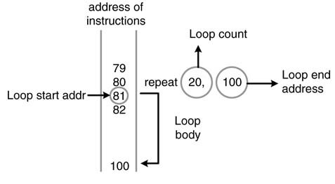
Figure 10.18 Loop machine to support a single loop instruction
To provide nested loop support, each register in the loop machine is replaced with a LIFO stack with unified stack pointer logic. The stacks store the loops’ start-addresses, end-addresses and counters for the nested loops and out put the values for the currently executing loop to the loop control logic. When the current loop finishes, the logic selects the outer loop and in this way it iteratively executes nested loops.
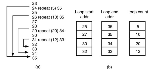
An example of nested loops that correspondingly fill the LIFO registers is given in Figure 10.19. The loop machine supports four nested loops with three sets of LIFOs for managing loops start addresses, loops end-addresses and loops counters. The design of the machine is given in Figure 10.20
Figure 10.19 Filling of the LIFOs for the four nested loops. (a) Instruction addresses and nested loop instructions. (b) Corresponding filling of the LIFO registers
All the three LIFOs in the loop machine work in lock step. The counter, when loaded with the loop count of the current loop instruction, decrements its value after executing the end instruction of the loop. The comparator sets the flag when the end of the loop is reached. Now based on the current value of the counter the two flags are assigned values. The loop-end-flag is set if the value of the counter is 0 and the machine is executing the last instruction of the loop. Similarly the loop-end-instr -flag is set if the processor is executing the end instruction but the counter value is still not 0. This signals the next-address logic to load the loop start-address as the next address to be executed. The state machine branches back to execute the loop again.
10.7 Examples
10.7.1 Design for Motion Estimation
Motion estimation is the most computationally intensive component of video compression algorithms and so is a good candidate for hardware mapping [4–6]. Although there are techniques for searching the target block in a pre-stored reference frame, a full-search algorithm gives the best result. This performs an exhaustive search for a target macro block in the entire reference frame to find the best match. The architecture designed for motion estimation using a full motion search algorithm can also be used for template matching in a machine vision application.
The algorithm works by dividing a video frame of size Nh ×Nv into macro blocks of size N × M. The motion estimation (ME) algorithm takes a target macro block in the current frame and searchers for its closest match in the previous reference frame. A full-search ME algorithm searches the macro block in the current frame with the macro block taking all candidate pixels of the previous frame. The algorithm computes the sum of absolute differences (SAD) as the matching criterion by implementing the expression:
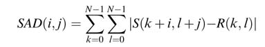
In this expression, R is the reference block in the current frame and S is the search area, which for the full-search algorithm is the entire previous frame while ignoring the boarder pixels. The ME algorithm computes the minimum value of SAD and stores the (i,j) as the point where the best match is found. The algorithm requires four summations over i, j, k and l.
Figure 10.21 shows an example. This design consists of a data movement block, two 2-D register files for storing the reference and the target blocks, and a controller that embeds a loop machine. The controller synchronizes the working of all blocks. The 2-D register file for the target block is extended in rows and columns making its size equal to (N ×1) × (N × 1) – 1 registers, whereas the size of the register file for the reference block is N ×N.
A full-search algorithm executes by rows and, after completing calculation for the current macro block, the new target block is moved one pixel in a row. While working in a row, for each iteration of the algorithm, N –1 previous columns are reused. The data movement block brings the new column to the extended-register-column in the ref-blk-reg-file. The search algorithm works in a daisy-chain and, after completing one row of operation, the data movement block starts in the opposite direction and fetches a new row in the extended-register-row in the register file. The daisy-chain working of the algorithm for maximum reuse of data in a target block is illustrated in Figure 10.22.
Figure 10.20 Loop machine with four-nested-loop support
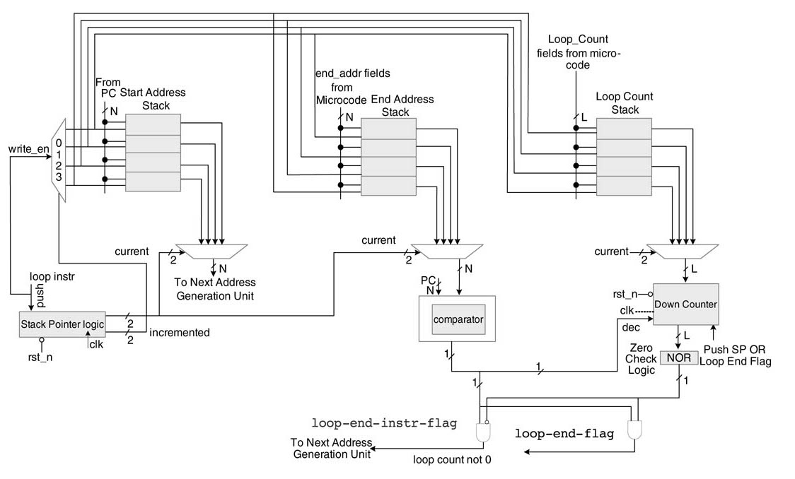
Figure 10.21 Micro-coded state machine design for full-search motion estimation algorithm
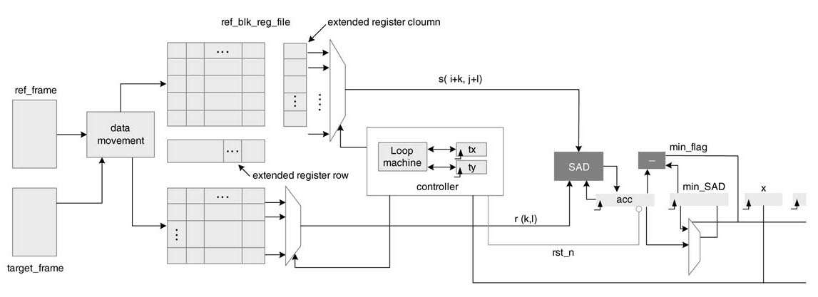
Figure 10.22 Full-search algorithm working in daisy-chain for maximum reuse of pixels for the target block
The toggle micro-code maintains the daisy-chain operation. This enables maximum reuse of data. The SAD calculator computes the summation, where the embedded loop machine in the controller automatically generates addressing for the two register files. The micro-code repeat8x8 maintains the addressing in the two register files and generates appropriate control signals to two multiplexers for feeding the corresponding values of pixels to the SAD calculator block. The micro-code abs_diff computes the difference and takes its absolute value for addition into a running accumulator. In each cycle, two of these values are read and their absolute difference is added in a running accumulator. After computing the SAD for the current block, its value is compared with the best match. If this value is less than the current best match, the value with the corresponding values in Tx and Ty registers in the controller are saved in Bx and By registers, respectively. The update_min micro-code performs this updating operation. The micro-program for ME application for a 256 × 256 size frame is given here:
Tx = 0;
Ty = 0;
repeat 256-8, LABELy
 repeat 256-8, LABELx
 acc = 0;
 repeat_8x8 //embedded repeat 8x8 times
 acc+=abs_diff;
 (Bx, By, minSAD)=updata_min(acc, best_match, Tx, Ty)
LABELx toggle(Tx++/-);
LABELy Ty++;
This program assumes that the controller keeps directing the data movement block to bring the new row or column to the corresponding extended-register-row or extended-register-column files in parallel for each iteration of the SAD calculation and the repeat8x8 appropriately performs modulo addressing in the register file for reading the pixels of the current target block from the register file for the target frame.
The architecture is designed in a way such that SAD calculation can be easily parallelized and the absolute difference for more than one value can be computed in one cycle.
10.7.2 Design of a Wavelet Processor
Another good example is the architecture of a wavelet processor. The processor performs wavelet transformations for image and video processing applications. There are various types of wavelet used [7–11], so efficient micro-program architectures to accelerate these applications are of special interest [12, 13]. A representative design is presented here for illustration.
A 2-D wavelet transform is implemented by two passes of a 1-D wavelet transform. The generic form of the 1-D wavelet transform passes a signal through a low-pass and a high-pass filter, h[n] and g[n], and then their respective outputs are down-sampled by a factor of 2. Figure 10.23(a) gives the 1-D decomposition of a 1-D signal x[n] into low- and high-frequency components. For the 2-D wavelet transform, the first each column of the image is passed through a set of filters and the output is down-sampled; then in the second pass the rows of the resultant image are passed though the same set of filters. The pixel values of the output image are called the ‘wavelet coefficients’. In a pyramid algorithm for computing wavelet coefficients for an image analysis application, an image is passed through multiple levels of 2-D wavelet transforms. Each level, after passing the image through two 1-D wavelet transforms, decimates the image by 2 in each dimension. Figure 10.23(b) shows 2-level 2-D wavelet decomposition in a pyramid algorithm. Similarly, Figures 2 10.23 (c) and, (d) shows the results of performing one-level and three-level 2-D wavelet transforms on an image.
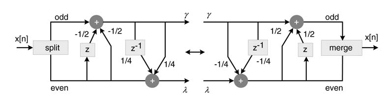
There are a host of FIR filters designed for wavelet applications. The lifting scheme is an efficient tool for designing wavelets [14]. As a matter of fact, every wavelet transform with FIR filters can be decomposed under the lifting scheme. Figure 10.24 shows an example of a 5/3 filter transformed as a lifting wavelet; this wavelet is good for image compression applications. Similarly, there is a family of lifting wavelets [12] that are more suitable for other applications, such as the 9/7 wavelet transform which is effective for image fusion applications (images of the same scene are taken from multiple cameras and then fused to one image for more accurate and reliable description) [14].
Figure 10.23 (a) One-dimensional wavelet decomposition. (b) Two-level 2-D pyramid decomposition. (c) One-level 2-D wavelet decomposition. (d) Three-level 2-D wavelet decomposition
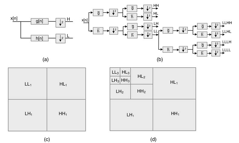
Figure 10.24 5/3 wavelet transform based on the lifting scheme
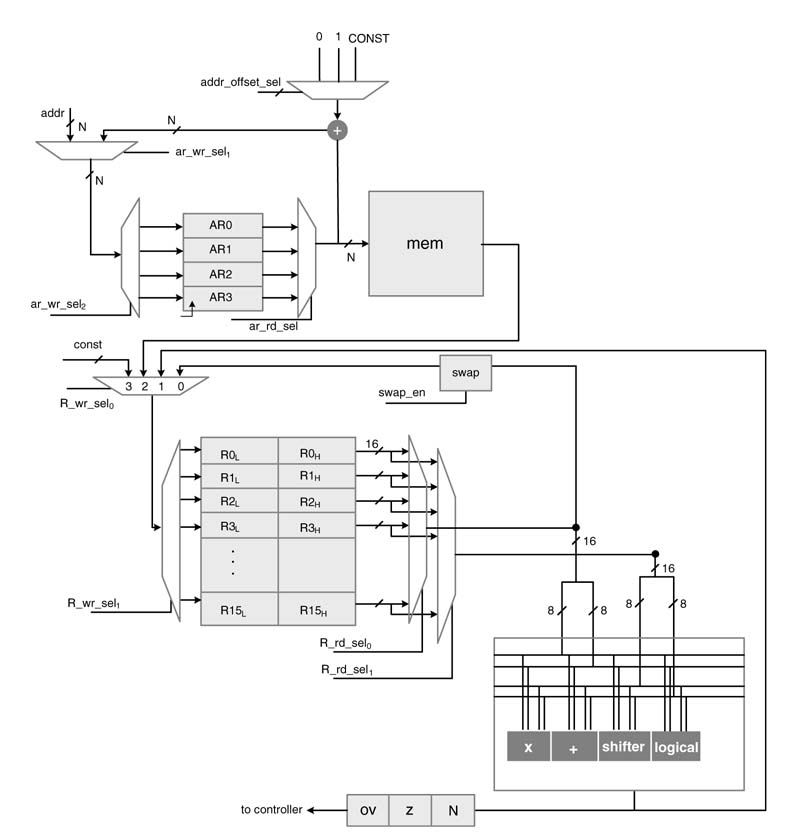
It is desired to design a programmable processor that can implement any such wavelet along with processing other signal processing functions. This requires the programmable processor to implement filters with different coefficients. For multimedia applications, multiple frames of images need to be processed every second. This requires several programmable processing elements (PEs) in architecture with shared and local memories placed in a configuration that enables scalability in inter-PE communications. This is especially so in video where multi-level pyramid-based wavelet transformations are performed on each frame. The coefficients of each lifting filter can be easily represented in 11 bits and an image pixel is represented in 8 bits. The multiplication results in a 19-bit number that can be scaled to either 8 or 16 bits. The register file of the PE is 16 bits wide for storing the temporary results. The final results are stored in memory as 8-bit numbers.
The instruction set of the PE is designed to implement any type of wavelet filtering as lifting transforms and similar signal processing algorithms. A representative architecture of the PE is given in Figure 10.25. The PE supports the following arithmetic instruction on a register file with 32-bit 16 registers:
Based on the arithmetic instruction, the PE sets the following overflow, zero and negative flags for use in the conditional instructions:
Flags: OV, Z,N
Figure 10.25 Datapath design for processing elements to compute a wavelet transform
The PE supports the following conditional and unconditional branch instructions:
if (Condi) jump Label,
else if (Condi) jump Label,
if(!Condi) jump Label,
else if (!Condi) jump Label,
else jump Label,
jump Label.
where Condi is one of the conditions 0V, Z and N, and Label is the address of the branch instruction.
The PE has four address registers and supports the following instructions:
Ari=addr
Ri=mem (Ari++)
Mem (Ari++)=Rj
Ri=mem (Ari)
Mem (Ari)=Rj
Ari=Ari+Const
For i = 0, 1, 2, 3
The PE supports four nested loops instructions of type repeat LABEL (COUNT). The instruction repeats the instruction block starting from the next instruction to the instruction specified by address LABEL, COUNT number of times. The PE also supports four nested subroutine calls and return instructions.
Exercises
Exercise 10.1
Write RTL Verilog code to implement the following folded design of a biquad filter (Figure 10.26.) A simple 2-bit counter is used to generate control signals. Assume a1, b1, a2 and b2 are 16-bit signed constants in Q1.15 format. The datapath is 16 bits wide. The multiplier is a fractional signed by signed multiplier, which multiplies two 16-bit signed numbers, and generates a 16-bit number in Q1.15 format. Use Verilog addition and multiplication operators to implement adder and multiplier. After multiplication, bring the result into the correct format by truncating the 32-bit product to a 16bit number. Testing your code for correctness, generate test vectors and associated results in Matlab and port them to your stimulus of Verilog or SystemVerilog.
Exercise 10.2
Design a micro-coded state machine based on a 4-deep LIFO queue to implement the following:
- A write into the LIFO writes data on the INBUS at the end of the queue.
- A delete from the LIFO deletes the last entry in the queue.
- A write and delete at the same time generates an error.
- A write in a full queue and delete from an empty queue generates an error.
- The last entry to the queue is always available at the OUTBUS.
Draw the algorithmic state machine (ASM) diagram. Draw the datapath, and give the micro-coded memory contents implementing the state machine design.
Exercise 10.3
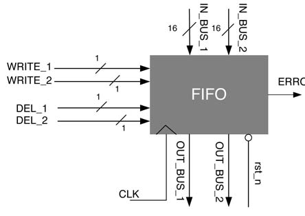
Design a micro-coded state machine-based FIFO queue with six 16-bit registers, R0 to R5. The FIFO has provision to write one or two values to the tail of the queue, and similarly it can delete one or two values from the head of the queue.
All the input and output signals of the FIFO are shown in Figure 10.27. A WRITE_1 writes the values on INBUS_1 at the tail of the queue in the R0 register, and a WRITE_2 writes values on IN_BUS_1 and IN_BUS_2 to the tail of the queue in registers R0 and R1, respectively, and appropriately adjusts already stored values in these registers to maintain the FIFO order. Similarly, a DEL_1 deletes one value and DEL_2 deletes two values from the head of the queue, and brings the next first-in values to OUT_BUS_1 and OUT_BUS_2. Only one of the input signals signal should be asserted at any point. List all erroneous/invalid requests and generate an error signal for these requests.
Figure 10.26 Folded design of a biquad filter in exercise 10.1
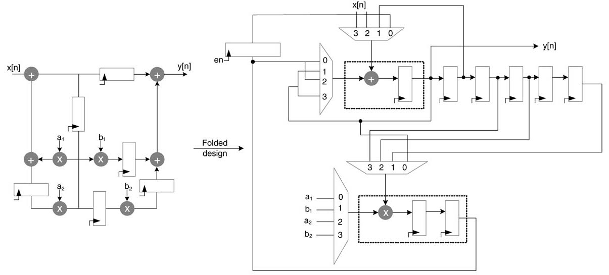
Figure 10.27 FIFO top-level design for exercise 10.3
1. Design an ASM chart to list functionality of the FSM.
2. Design the datapath and the micro-program-based controller for the design problem. Write the micro-codes for the design problem. Draw the RTL diagram of the datapath showing all the signals.
3. Code the design in RTL Verilog. Hierarchically break the top-level design into two main parts, datapath and controller.
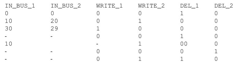
4. Write a stimulus and test the design for the following sequence of inputs:
Exercise 10.4
Design a micro-coded state machine for an instruction dispatcher that reads a 32-bit word from the instruction memory. The instructions are arranged in two 32-bit registers, IR0 and IR1. The first bit of the instruction depicts whether the instruction is 8-bit, 16-bit or 32-bit. The two instruction registers always keep the current instruction in IR1, while the LSB of the instruction is moved to the LSB of IR1.
Exercise 10.5
Design a micro-coded state machine to implement a bit-serial processor with the following micro-codes:
 Repeat (count) END_ADDRESS
 Call Subroutine at ADDERSS
 return
where R1, R2 and R3 are 8-bit registers, and indexes i, j, k = 0,..., 7 specify a particular bit of these registers.
Exercise 10.6
Design a micro-coded state machine that operates on a register file with eight 8-bit registers. The machine executes the following instructions:
Call Subroutine ADDRESS
return
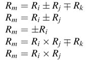
All multiplications are fractional multiplications that multiply two Q-format 8-bit signed numbers and produce an 8-bit signed number. In the register file, i, j, k =0,..., 7, and correspondingly Ri, Rj, Rk and Rm are any one of the eight registers.
Exercise 10.7
Design a micro-program state machine that supports the following instruction set:
Load R5=ADDRESS
Jump R5
If (R4 == 0) jump R5
If (R4 > 0) jump R5
Call subroutine R5 and return support
R1 to R5 are 8-bit registers. A branch address or subroutine address can be written in R5 using a load instruction. As given in the instruction set, jump and subroutine instructions are developed to use the contents of R5 as address of the next instruction. The conditions are based on the content of R4. Draw the RTL diagram of the datapath and micro-programmed state machine. Show all the control signals. Specify the instruction format and size. The datapath should be optimal using only one carry propagate adder (CPA) by appropriately using a compression block to compress the number of operands to two.
Exercise 10.8
Design a micro-coded state-machine based design, with the following features.
1. There are three register files, P, Q and R. Each register file has four 8-bit registers.
2. There is an adder and logic unit to perform addition, subtraction, AND, OR and XOR operations.
3. There is 264 deep micro-code memory.
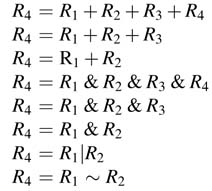
4. The state machine supports the following instructions:
(a) Load constant into ith register of P or Q:
Pi = const
Qi = const
(b) Perform any arithmetic or logic operation given in (2) on operands in register files P and Q, and store the result in register file R:
Ri = Pj op Qk
(c) Unconditional branch to any address LABEL in microcode memory:
goto LABEL
(d) Subroutine call support, where subroutine is stored at address LABEL:
call subroutine LABEL
return
(e) Support repeat instruction, for repeating a block of code COUNT times:
repeat (COUNT) LABEL
LABEL is the address of the last instruction in the loop.
Exercise 10.9
Design a micro-programmed state machine to support 4-deep nested loops and conditional jump instructions with the requirements given in (1) and (2), respectively. Draw an RTL diagram clearly specifying sizes of instruction register, multiplexers, comparators, micro-PC register, and all other registers in your design.
1. The loop machine should support conditional loop instructions of the format:
if (CONDi) repeat END_LABEL COUNT
The micro-code checks COND i = 0,1,2,3 and, if it is TRUE, the state machine repeats COUNT times a block of instructions starting from the next instruction to the instruction labeled with END_LABEL. Assume the size of PM is 256 words and a 6-bit counter that stores the COUNT. Also assume that, in the instruction, 10bits are kept for the datapath-related instruction. If CONDi is FALSE, the code skips the loop and executes the instruction after the instruction addressed by END_LABEL.
2. Add the following conditional support instruction in the instruction set:
if (CONDi) Jump LABEL
if (!CONDi) Jump LABEL
jump LABEL
Exercise 10.10
Design a micro-program architecture with two 8-bit input registers R1 and R2, an 8-bit output register R3, and a 256-word deep 8-bit memory MEM. Design the datapath and controller to support the following micro instructions. Give op-code of each instruction, draw the datapath, and draw the micro-coded state machine clearly specifying all control signals and their widths.
- Load R1 Addr loads the content of memory at address Addr into register R1.
- Load R2 Addr loads the content of memory at address Addr into register R2.
- Store R3 Addr stores the content of register R3 into memory at address Addr.
- Arithmetic and logic instructions Add, Mult, Sub, OR and AND take operands from registers R1 and R2 and store the result in register R3.
- The following conditional and unconditional branch instructions: Jump Label, Jump Label if (R1==0), Jump Label if (R2==0), Jump Label if (R3==0).
- The following conditional and unconditional subroutine and return instructions: Call Label, Call Label if (R1>0), Call Label if (R2>0),Call Label if (R3>0),Return, Return if (R3<0), Return if (R3==0).
Exercise 10.11
Using an instruction set of the wavelet transform processor, write a subroutine to implement 5/3 wavelet transform of Figure 10.24. Use this subroutine to implement a pyramid coding algorithm to decompose an image in three levels.
References
1. M. Froidevaux and J. M. Gentit, “MPEG1 and MPEG2 system layer implementation trade-off between micro-coded and FSM architecture,” in Proceedings of IEEE International Conference on Consumer Electronics, 1995, pp. 250–251.
2. M. A. Lynch, Microprogrammed State Machine Design, 1993, CRC Press.
3. N. Kavvadias and S. Nikolaidis, “Zero-overhead loop controller that implements multimedia algorithms,” IEEE Proceedings on Computers and Digital Technology, 2005, vol. 152, pp 517–526.
4. M. A. Daigneault, J. M. P. Langlois and J. P. David, “Application-specific instruction set processor specialized for block motion estimation,” in Proceedings of IEEE International Conference on Computer Design, 2008, pp. 266–271.
5. T.-C. Chen, S.-Y. Chien, Y.-W. Huang, C.-H. Tsai and C.-Y. Chen, “Fast algorithm and architecture design of low-power integer motion estimation for H.264/AVC,” IEEE Transactions on Circuits and Systems for Video Technology, 2007, pp. 568–577.
6. C.-C. Cheng, Y. J. Wang and T.-S. Chang, “A fast algorithm and its VLSI architecture for fractional motion estimation for H.264/MPEG-4 AVC video coding,” IEEE Transactions on Circuits and Systems for Video Technology, 2007, pp. 578–583.
7. O. Rioul and M. Vetterli, “Wavelets and signal processing,” IEEE Signal Processing Magazine, 1991, vol. 8, pp. 14–38.
8. I. Daubechies, Ten Lectures on Wavelets, 1992, Society of Industrial and Applied Mathematics (SIAM).
9. S. Mallat, A Wavelet Tour of Signal Processing, 1998, Elsevier Publishers, UK.
10. S. Burrus, R. Gopinath and H. Guo, Introduction to Wavelets and Wavelet Transforms: a Primer, 1997, Prentice-Hall.
11. M. Vetterli and J. Kovacevic, Wavelets and Sub-band Coding, 1995, Prentice-Hall.
12. S.-W. Lee and S.-C. Lim, “VLSI design of a wavelet processing core,” IEEE Transactions on Circuits and Systemsfor Video Technology, 2006, vol. 16, pp. 1350–1361.
13. H. Olkkonen, J. T. Olkkonen and P. Pesola, “Efficient lifting wavelet transform for microprocessor and VLSI applications,” IEEE Signal Processing Letters, 2005, vol. 12, pp. 120–122.
14. W. Sweldens, “The lifting scheme: a custom-design construction of biorthogonal wavelets,” Applied and Computational Harmonic Analysis Journal, 1996, vol. 3, pp. 186–200.