
4
Mapping on Fully Dedicated Architecture
4.1 Introduction
Although there are many applications that are commonly mapped on field-programmable gate arrays (FPGAs) and application-specific integrated circuits (ASICs), the primary focus of this book is to explore architectures and design techniques that implement real-time signal processing systems in hardware. A high data rate, secure wireless communication gateway is a good example of a signal processing system that is mapped in hardware. Such a device multiplexes several individual voice, data and video channels, performs encryption and digital modulation on the discrete signal, up-converts the signal, and digitally mixes it with an intermediate frequency (IF) carrier.
Thes types of digital design implement complex algorithms that operate on large amounts of data in real time. For example, a digital receiver for a G703 compliant E3 microwave link needs to demodulate 34.368Mbps of information that were modulated using binary phase-shift keying (BPSK) or quadrature phase shift keying (QPSK). The system further requires forward error-correction (FEC) decoding and decompression along with several other auxiliary operations in real time.
These applications can be conveniently conceived as a network of interconnected components. For effective HW mapping, these components should be placed to work independently of other components in the system. The Kahn Process Network (KPN) is the simplest way of synchronizing their interworking. Although the implementation of a system as a KPN theoretically uses an unbounded FIFO (first-in/first-out) between two components, several techniques exist to optimally size these FIFOs. The execution of each component is blocked on a read operation on FIFOs on incoming links. A KPN also works well to implement event-driven and multi-rate systems. For signal processing applications, each component in the KPN implements one distinct block of the system. For example, the FEC in a communication receiver is perceived as a distinct block. This chapter gives a detailed account of the KPN and demonstrates its effectiveness and viability for digital system design with a case study.
In addition to this, for implementing logic in each block, the algorithm for the block can first be described graphically. There are different graphical ways of representing signal processing algorithms. The dataflow graph (DFG), signal flow graph, block diagram and data dependency graph (DDG) are a few choices for the designer. These representations are quite similar but have subtle differences. This chapter gives an extensive account of DFG and its variants. Graphical representation of the algorithm in any of these formats gives convenient visualization of algorithms for architecture mapping.
For blocks that need to process data at a very high data rate, the fastest achievable clock frequency is almost the same as the number of samples the block needs to process every second. For example, a typical BPSK receiver needs four samples per symbol to decode bits; for processing 36.5 Mbps of data, the receiver must process 146 million samples every second. The block implementing the front end of such a digital receiver is tasked to process even higher numbers of samples per symbol. In these applications the designer aims to achieve a clock frequency that matches the sampling frequency. This matching eases the digital design of the system, because the entire algorithm then requires one-to-one mapping of algorithmic operations to HW operators. This class of architecture is called ‘fully dedicated architecture’ (FDA). The designer, after mapping each operation to a HW operator, may need to appropriately place pipeline registers to bring the clock frequency equal to the sampling frequency.
The chapter describes this one-to-one mapping and techniques and transformations for adding one or multiple stages of pipelining for better timing. The scope of the design is limited to synchronous systems where all changes to the design are mastered by either a global clock or multiple clocks. The focus is to design digital logic at register transfer level (RTL). The chapter highlights that the design at RTL should be visualized as a mix of combinational clouds and registers, and the developer then optimizes the combinational clouds by using faster computational units to make the HW run at the desired clock while constraining it to fit within a budgeted silicon area. With feedforward algorithms the designer has the option to add pipeline registers in slower paths, whereas in feedback designs the registers can be added only after applying certain mathematical transformations. Although this chapter mentions pipelining, a detail treatment of pipelining and retiming are given exclusive coverage in Chapter 7.
4.2 Discrete Real-time Systems
A discrete real-time system is constrained by the sampling rate of the input signal acquired from the real world and the amount of processing the system needs to perform on the acquired data in real time to produce output samples at a specified rate. In a digital communication receiver, the real-time input signal may be modulated voice, data or video and the output is the respective demodulated signal. The analog signal is converted to a discrete time signal using an analog-to-digital (A/D) converter.
In many designs this real-time discrete signal is processed infixed-size chunks. The time it takes to acquire a chunk of data and the time required to process this chunk pose a hard constraint on the design. The design must be fast enough to complete its processing before the next block of data is ready for its turn for processing. The size of the block is also important in many applications as it causes an inherent delay. A large block size increases the delay and memory requirements, whereas a smaller block increases the block-related processing overhead. In many applications the minimum block size is constrained by the selected algorithm.
In a communication transmitter, a real-time signal – usually voice or video – is digitized and then processed by general-purpose processors (GPPs), ASICs or FPGAs, or any combination of these. This processed discrete signal is converted back to an analog signal and transmitted on a wired or wireless medium.
A signal processing system may be designed as single-rate or multiple-rate. In a single-rate system, the numbers of samples per second at the input and out put of the system are the same, and the number of samples per second does not change when the samples move from one block to another for processing. Communication systems are multi-rate systems: data is processed at different rates in different blocks. For each block the number of samples per second is specified. Depending on whether the system is a transmitter or a receiver, the number of samples per second may respectively increase or decrease for subsequent processing. For example, in a digital front end of a receiver the samples go through multiple stages of decimation, and in each stage the number of samples per second decreases. On the transmitter side, the number of samples per second increases once the data moves from one block to another. In a digital up-converter, this increase in number of samples is achieved by passing the signal through a series of interpolation stages. The number of samples each block needs to process every second imposes a throughput constraint on the block. For speech the data acquisition rate varies from 8 kHz to 16 kHz, and samples are quantized from 12-bit to 16-bit precision. For voice signals, like CD-quality music, the sampling rate goes to 44.1 kHz and each sample is quantized using 16-bit to 24-bit precision. For video signals the sampling rate further increases to 13.4 MHz with 8-bit to 12-bit of precision. Figure 4.1 illustrates the periodic sampling of
Figure 4.1 Periodic sampling of (a) 1-D signal; (b) 2-D signal; (c) 3-D signal
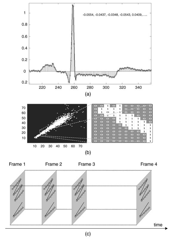
Figure 4.2 Real-time communication system
a one-dimensional electrocardiogram signal (ECG), a 2-D signal of a binary image, and 3-D signal of a video.
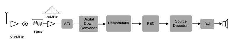
Another signal of interest is the intermediate frequency signal that is output from the analog front end (AFE) of a communication system. A communication receiver is shown in Figure 4.2. This IF signal is at a frequency of 70 MHz. It is discretized using an A/D converter. Adhering to the Nyquist sampling criterion, the signal is acquired at greater than twice the highest frequency of the signal at IF. In many applications, band-pass sampling is employed to reduce the requirement for high-speed A/D converters [1, 2]. Band-pass sampling is based on the bandwidth of an IF signal and requires the A/D converter to work at a much lower rate than the sampling at twice the highest frequency content of the signal. The sampling rate is important from the digital design perspective as the hardware needs to process data acquired at the sampling rate. This signal acquired at the intermediate frequency goes through multiple stages of decimation in a digital down-converter. The down-converted signal is then passed to the demodulator block, which demodulates the signal and extracts bits. These bits then go through an FEC block. The error-corrected data is then passed to a source decoder that decompresses the voice and passes it to a D/A converter for playing on a speaker.
4.3 Synchronous Digital Hardware Systems
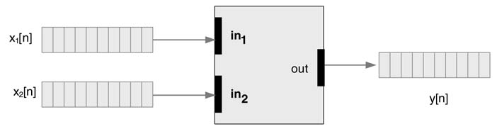
In many instances, signal processing applications are mapped on synchronous digital logic. The word ‘synchronous’ signifies that all changes in the logic are controlled by a circuit clock, and ‘digital’ means that the design deals only with digital signals. Synchronous digital logic is usually designed at the register transfer level (RTL) of abstraction. At this level the design consists of combinational clouds executing computation in the algorithm and synchronous registers storing intermediate values and realizing algorithmic delays of the application.
Figure 4.3 shows a hypothetical example depicting mapping of a DSP algorithm as a synchronous digital design at RTL. Input values x 1[n ]... x 4[n ] are synchronously fed to the logic. Combinational blocks 1 to 5 depict computational units, and registers a to g are algorithmic delays.
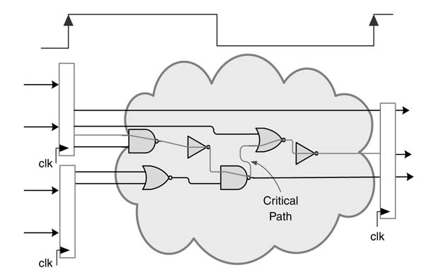
Figure 4.4 shows a closer look into a combinational cloud and registers where all inputs are updated at the positive edge of the clock. The combinational cloud consists of logic gates. The input to the cloud are discrete signals, stored in registers. While passing through the combinational logic these signals experience different delays on their respective paths. It is important for all the signals at the output wires to be stable before the next edge of the clock occurs and the output is latched in the output register. The clock period imposes a strict constraint on the longest or the slowest (critical) path. The critical path thus constrains the fastest achievable clock frequency of a design.
Figure 4.3 Register transfer level design consisting of combinational blocks and registers
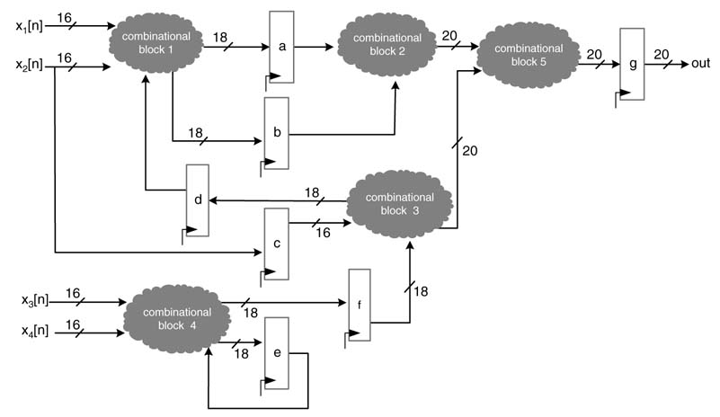
Figure 4.4 Closer look at a combinational cloud and registers depicting the critical path
4.4 Kahn Process Networks
4.4.1 Introduction to KPN
A system implementing a streaming application is best represented by autonomously running components taking inputs from FIFOs on input edges and generating output in FIFOs on the output
Figure 4.5 A node fires when sufficient tokens are available at all its input FIFOs
edges. The Kahn Process Network (KPN) provides a formal method to study this representation and its subsequent mapping in digital design.
The KPN is a set of concurrently running autonomous processes that communicate among themselves in a point-to-point manner over unbounded FIFO buffers, where the synchronization in the network is achieved by a blocking read operation and all writes to the FIFOs are non-blocking. This provides a very simple mechanism for mapping of an application in hardware or software. The reads and writes confined to the KPN also elevates the design from the use of a complicated scheduler. A process waits in a blocking read mode for the FIFOs on each of its incoming links to get a predefined number of samples, as shown in Figure 4.5. All the nodes in the network execute after their associated input FIFOs have acquired enough data. This execution of a node is called firing, and samples are called tokens . Thus, firing produces tokens and they are placed in respective output FIFOs.
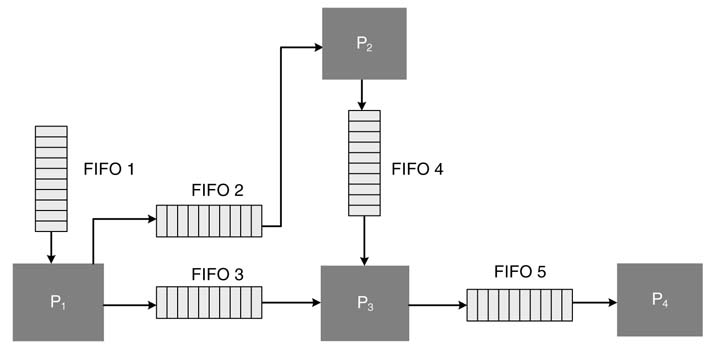
Figure 4.6 shows a KPN implementing a hypothetical algorithm consisting of four processes. Process P1 gets the input data stream in FIFO1 and, after processing a defined number of tokens, writes the result in output FIFO2 and FIFO3 on its links to processes P2 and P3, respectively. Process P2 waits for a predefined number of tokens in FIFO2 and then fires and writes the output tokens in FIFO4. Process P3 performs blocking read on FIFO3 and FIFO4, and then fires and writes data in FIFO5 for process P4 to execute its operation.
Figure 4.6 Example of a KPN with four processes and five connected FIFOs
Confining the buffers of the FIFOs to minimum size without affecting the performance of the network is a critical problem attracting the interest of researchers. A few solutions have been proposed [4, 5].
The KPN can also be implemented in software, where each process executes in a separate thread. The process, in a sequence of operations, waits on a read from a FIFO and, when the FIFO has enough samples, the thread performs a read operation and executes. The results are written into output FIFO. The KPN also works well in the context of mapping of a signal processing algorithm on reconfigurable platforms.
4.4.2 KPN for Modeling Streaming Applications
To map a streaming application as a KPN, it is preferable to first implement the application in a high-level language. The code should be broken down into distinguishable blocks with clearly identified streams of input and output data. This formatting of the code helps a designer to map the design as a KPN in hardware. The MATLAB® code below implements a hypothetical application:
N = 4*16;
K = 4*32;

% source node
for i=1:N
 for j=1:K
 x(i,j)= src_x ();
 end
end

% processing block 1
for i=i:N
 for j=1:K
 y1(i,j)=func1(x(i,j));
 end
end

% processing block 2
for i=1:N
 for j=1:K
 y2(i,j)=func2(y1(i,j));
 end
end
% sink block
m=1;
for i=1:N
 for j=1:K
 y(m)=sink (x(i,j), y1(i,j), y2(i,j));
 m=m+1;
 end
end
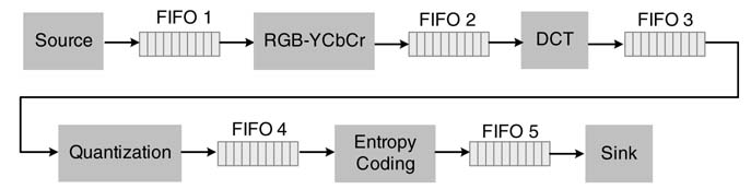
Figure 4.7 KPN implementing JPEG compression
4.4.2.1 Example: JPEG Compression Using KPN
Although KPN best describes distributed systems, it is also suited well to model streaming applications. In these, different processes in the system, in parallel or in a sequence, incrementally transform a stream of input data. Here we look at an implementation of the Joint Photographic Experts Group (JPEG) algorithm to demonstrate the effectiveness of a KPN for modeling streaming applications.
A raw image acquired from a source is saved in FIFO1, as shown in Figure 4.7 The algorithm is implemented on a block-by-block basis. This block is read by node 1 that transforms each pixel of the image from RGB to YCbCr and stores the transformed block in FIFO2. Now node 2 fires and computes the discrete cosine transform (DCT) of the block and writes the result in FIFO3. Subsequently node 3 and then node 4 fire and compute quantization and entropy coding and fill FIFO4 and FIFO5, respectively.
To implement JPEG, MATLAB ® code is first written as distinguishable processes. Each process is coded as a function with clearly defined data input and output. The designer can then easily implement FIFOs for concurrent operation of different processes. This coding style helps the user to see the application as distinguishable and independently running processes for KPN implementation. Tools such as Compaan can exploit the code written in this subset of MATLAB® to perform profiling, HW/SW partitioning and the SW code generation. Tools such as Laura can be used subsequently for HW code generation for FPGAs [6, 7].
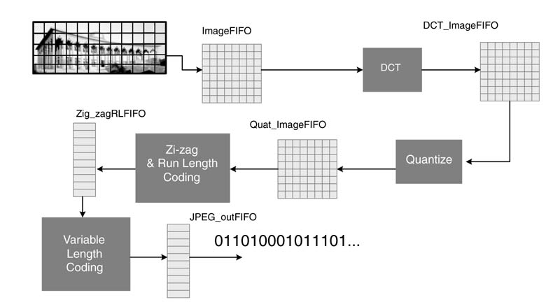
A representative top-level code in MATLAB® is given below (the code listing for functions zigzag_runlength and VLC_huffman are not given and can be easily coded in MATLAB®:
Q=[8 36 36 36 39 45 52 65;
36 36 36 37 41 47 56 68;
36 36 38 42 47 54 64 78;
36 37 42 50 59 69 81 98;
39 41 47 54 73 89 108 130;
45 47 54 69 89 115 144 178;
53 56 64 81 108 144 190 243;
BLK_SZ = 8; % block size

imageRGB = imread(peppers.png’); % default image
figure, imshow(imageRGB);
title(Original Color Image’);
ImageFIFO = rgb2gray(RGB);
figure, imshow(ImageFIFO);
title(Original Gray Scale Image’);
fun = @dct2;
figure, imshow(DCT_ImageFIFO);
title(‘DCT Image’);
QuanFIFO = blkproc(DCT_FIFO, [BLK_SZ BLK_SZ], ‘round(x./P1)’, Q);
figure, imshow(QuanFIFO);

fun = @zigzag_runlength;
zigzagRLFIFO = blkproc(QuanFIFO, [BLK_SZ BLK_SZ], fun);
% Variable length coding using Huffman tables
JPEGoutFIFO = VLC_huffman(zigzagRLFIFO, Huffman_dict);
This MATLAB® code can be easily mapped as a KPN. A graphical illustration of this KPN mapping is shown in Figure 4.8 To conserve FIFO sizes for hardware implementation, the processing is performed on a block-by-block basis.
4.4.2.2 Example: MPEG Encoding
This section gives a top-level design of a hardware implementation of the MPEG video compression algorithm. Steps in the algorithm are given in Figure 4.9.
Successive video frames are coded as I and P frames. The coding of an I frame closely follows JPEG implementation, but instead of using a quantization table the DCT coefficients are quantized by a single value. This coded I frame is also decoded following the inverse processes of quantization and DCT. The decoded frame is stored in motion video (MV) memory.
For coding a P frame, first the frame is divided into macro blocks. Each block (called a target block) is searched in the previously decoded and saved frame in MV memory. The block that matches best with the target block is taken as a reference block and a difference of target and
Figure 4.8 Graphical illustration of a KPN implementing the JPEG algorithm on block by block basis
reference block is computed. This difference block is then quantized and Huffman-coded for transmission. The motion vector refereeing the block in the reference frame is also transmitted. At the receiver the difference macro-block is decoded and then added in the reference block for recreation of the target block.
Figure 4.9 (Continued )
Figure 4.9 Steps in video compression. (a) Video is coded as a mixture of Intra-Frames (I-Frames) and Inter- or Predicted Frames (P-Frames). (b) I-Frame is coded as JPEG frame. (c) The I-Frame and all other frames are also decoded for coding of P-Frame, KPN implementation with FIFO’s is given. (d) For P-Frame coding, the frame is divided into sub-blocks and each block is searched in the previously self-decoded frame. The target block is searched in the previous block for best match. This block in called the reference block. (e) The difference of target and reference block is coded as a JPEG block and the motion vector is also coded and transmitted with the coded block
While encoding a P frame, the coder node in the KPN implementation fires only when it has tokens in the motion vector FIFO and the QuantFIFO. Similarly the difference node executes only while coding a P frame and fires after the target block is written in the macroBlockFIFO, and the MV search block finds the best match and writes the best match block in best_match_BlockFIFO. For the I frame, a macro block in marcoBlockFIFO is directly fed to the DCT block and the coder fires once it has data in DCTFIFO. The rest of the blocks in the architecture also fire when they have data in their corresponding input FIFOs.
In a streaming application, MPEG coded information is usually transferred on a communication link. The status of the transmit buffer implemented as FIFO is also passed to a controller . If the buffer still has more than a specified number of bits to transfer, the controller node fires and changes the quantization level of the algorithm to a higher value. This helps in reducing the bit rate of the encoded data. Similarly, if the buffer has fewer than the specified number of bits, the controller node fires and reduces the quantization level to improve the quality of streaming video. The node also controls the processing of P or I frames by the architecture.
This behavior of the controller node sets it for event-driven triggering, where the rest of the nodes synchronously fire to encode a frame. A KPN implementation very effectively mixes these nodes and without any elaborate scheduler implements the algorithm for HW/SW partitioning and synthesis.
4.4.3 Limitations of KPN
The classical KPN model presents three serious limitations [8]:
- First, reading data requires strict adherence to FIFO, which constrains the reads to follow a sequential order from the first value written in the buffer to the last. Several signal processing algorithms do not follow this strict sequencing, an example being a decimation-in-time FFT algorithm that reads data in bit-reverse addressing order [9].
- Second,aKPN network also assumes that once avalue isread from the FIFO,itisdeleted. In many signal processing algorithms data is used multiple times. For example, a simple convolution algorithm requires multiple iterations of the algorithm to read the same data over and over again.
- Third, a KPN assumes that all values will be read, whereas in many algorithms there may be some values that do not require any read and data is read sparsely.
4.4.4 Modified KPN and MPSoC
Many researchers have proposed simple workarounds to deal with the limitations of the KPN noted above. The simplest of all is to use local memory M in the processor node D for keeping a copy of its input FIFO’s data. The processor node (or an independent controller) makes a copy of the data in local memory of the processor, in case the data has a chance of experiencing any of the above limitations.
Multi-processor system-on-chip (MPSoC) is another design of choice for many modern high-throughput signal processing and multimedia applications [10, 11]. These appliations employ some form of KPN to model the problem, and then the KPN, in many design methodologies, is automatically translated into MPSoC. A representative design is shown in Figure 4.10. Each processor has its local memory M, a memory controller (MC) and requisite FIFOs. It is connected to the FIFOs of other processors through a cross bar switch, a P2P network, a shared bus or a more elaborate network-on-chip (NOC) fabric. Each processor has a communciation controller (CC) that implements arbitration logic for sending data to FIFOs of other processors. The implementation is structured as tiles of these basic units. A detailed discussion on NoC design is given in Chapter 13.
Figure 4.10 Modified KPN eliminating key limitations of the classical KPN configuration
4.4.5 Case Study: GMSK Communication Transmitter
The KPN configuration is used here in the design of a communication system comprising a transmitter and a receiver. As there is similarity in the top-level design of transmitter and receiver is the same, this section describes only the top-level design of the transmitter.
At the top level the KPN very conveniently models the design by mapping different blocks in the transmitter as autonomously executing hardware building blocks. FIFOs are used between two adjacent blocks and local memory in each block is used to store intermediate results. A producer block, after completing its execution, writes output data in its respective FIFO and notifies its respective consumer block to fire.
The transmitter system implements baseband digital signal processing of a Gaussian minimum shift-keying (GMSK) transmitter. The system takes the input data and modulates it on to an intermediate frequency of 21.4 MHz. The input to the system is an uninterrupted stream of digitized data. The input data rate is variable from 16 kbps up to 8 Mbps. In the system the data incrementally undergoes a series of transformations, such as encryption, forward error correction, framing, modulation and quadrature mixing.
The encryption module performs 256-bit encryption on a 128-bit input data block. A 256-bit key is input to the block. The encryption module expands the key for multiple rounds of encryption operation. The FEC performs ‘block turbo code’ (BTC) for a block size of m × n with values of m and n to be 11,26 and 57. For different options of m and n the block size ranges from 121 to 3249 bits. The encoder adds redundant bits for error correction and changes the size of the data to k ×l , where k and l can take values 16,32 or 64. For example, the user may configure the block encoder to input 11 ×57 data and encode it to 16 ×64. The user can also enable the interleaver that takes the data arranged row-wise and then reads it column-wise.
As AES (advanced encryption standard) block does not fall in the integer multiple of FEC boundaries, so two levels of marker are inserted. One header marks the start of the AES block and the other indicates the start of the FEC block. For example, each 128-bit AES block is appended with an 8-bit marker. Similarly, each FEC block is independently appended with a 7-bit marker.
The last module in the transmitter is the framer. This appends a 16-bit of frame header that marks the start of a frame.
The objective of presenting this detail is to show that each node works on a different size of data buffer. The KPN implementation performs a distributed synchronization where a node fires when its input FIFO has enough tokens. The same FIFO keeps collecting tokens from the preceding node for the next firing.
In realizing the concept, the design is broken down into autonomously running HW building blocks of AES, FEC encoder, framer, modulator and mixer. Each block is implemented as an application-Specific processor (ASP). ASPs for AES and FEC have their local memories. The design is mapped on an FPGA. A dual-port RAM (random-access memory) block is instantiated between two ASPs and configure to work as a FIFO. A 1-bit signal is used between producer and consumer ASPs for notification of completion of the FIFO write operation.
A detailed top-level design of the transmitter revealing a KPN structure is shown in Figure 4.11.
The input data is received on a serial interface. The ASPaesinterface collects these bits, forms them in a one-byte word and writes the word in FIFOAes. After the FIFO collects 128 bits (i.e. 16 bytes of data) the ASPaes fires and starts its execution. As writes to the FIFO are non-blocking, thus the interface keeps collecting bits, forms them in one-byte words and writes the words in the FIFO. The encryption key is expended at the initialization and is stored in a local memory of ASPAes labeled as MEMaes. The internal working of the ASPaes is not highlighted in this chapter as the basic aim of the section is to demonstrate the top-level modeling of the design as KPN. A representative design of ASPaes is given in Chapter 13.
The next processor in the sequence is ASPFec. The processor fires after its FIFO stores sufficient number of samples based on the mode selected for BTE. For example, the 11×11 mode requires 121 bits. Each firing of ASPaes produces 128 bits and an 8-bit marker is attached to indicate the start of the AES block. ASPFec fires once and uses 121 bits. The remaining 15 bits are left in the FIFO. In the next firing these 15 bits along with 106 bits from current AES frame are used and 30 bits are left in the FIFO. The number of remaining bits keeps increasing, and after a number of iterations they make a complete FEC block that requires an additional firing of the ASPFec. The FEC block is a multi-rate block as it adds additional bits for error correction at the receiver. For the case in consideration, 121 bits generate 256 bits at the output.
At the completion of encoding, the ASPFec notifies the ASPFramer. The ASPFramer also waits to collect the defined number of bits before it fires. It also appends a 16-bit header to the frame of data from ASPFec for synchronization at the receiver. The framer writes a complete frame of data in a buffer. From here onward the processing is done on a bit-by-bit basis. The GMSK modulator first filters the non-return-to-zero (NRZ) data using a Gaussian low-pass filter and the resultant signal is then frequency modulated (FM). The bandwidth of the filter is chosen in such a way that it yields a narrowband GMSK signal given by:
![]()
where fc is the carrier frequency, Pc is the carrier power and φs(t) is the phase modulation given by:
where fd is the modulation index and is equal to 0.5 for GMSK, ak is the binary data symbol and is equal to ±1, and g(.) is the Gaussian pulse. A block diagram of the GMSK baseband modulator is shown in Figure 4.12.
Figure 4.11 Detailed top-level design of the transmitter modeled as a KPN
Figure 4.12 GMSK modulator block comprising of up-converter, Gaussian filter and phase modulator
The complex baseband modulated signal is passed to a digital quadrature mixer. The mixer multiplies the signal by exp (jω on). The mixed signal is passed to a two-channel D/A converter. The quadrature analog output from the D/A is mixed again with an analog quadrature mixer for onward processing by the analog front end (AFE).
The processors are carefully designed to work in lock step without losing any data. The processing is faster than the data acquisition rate at the respective FIFOs. This makes the processors wait a little after completing execution on a set of data. The activation signals from the input FIFOs after storing the required number of bits make the connected processors fire to process the data in the FIFO.
4.5 Methods of Representing DSP Systems
4.5.1 Introduction
There are primarily two common methods to represent and specify DSP algorithms: language-driven executable description and graphics or flow-graph-driven specification.
The language-driven methods are used for software development, high-level languages being used to code algorithms. The languages are either interpretive or executable. MATLAB® is an example of an interpretive language. Signal processing algorithms are usually coded in MATLAB®. As the code is interpreted line by line, execution of the code has considerable overheads. To reduce these it is always best to write compact MATLAB® code. This requires the developer to avoid loops and element-by-element processing of arrays, and instead where possible to use vectorized code that employs matrices and arrays in all computations. Besides using arrays and matrices, the user can predefine arrays and use compiled MEX (MATLAB® executable) files to optimize the code.
For a computationally intensive part of the algorithm, where vectorization of the code is not possible, the user may want to optimize by creating MEX files from C/C + + code or already written MATLAB® code. If the user prefers to manually write the code in C/C + +, a MEX application programming interface (API) is used for interfacing it with the rest of the code written in MATLAB®. In many design instances it is more convenient to automatically generate the MEX file from already written MATLAB® code. For computationally intensive algorithms, the designer usually prefers to write the code in C/C + +. As in these languages the code is compiled for execution, the executable runs much faster than its equivalent MATLAB® simulation.
In many designs the algorithm developer prefers to use a mix of MATLAB® and C/C + + using the MATLAB® Complier. In these instances visualization and other peripheral calculations are performed in MATLAB® and number-crunching routines are coded in C/C + +, compiled and then called from the MATLAB® code. The exact semantics of MATLAB® and C/C + + are not of much interest in hardware mapping. The main focus of this chapter is graphical representation of DSP algorithms, so the description of exact semantics of procedural languages is left for the readers to learn from other resources. It is important to point out that there are tools such as Compaan that convert a code written in a subset of MATLAB® or C constructs to HW description [12].
Although language-driven executable specifications have wider acceptability, graphical methods are gaining ground. The graphical methods are especially convenient for HW mapping and understanding the working and flow of the algorithm. A graphical representation is the method of choice for developing optimized hardware, code generation and synthesis.
Another motivation to learn about the graphical representation comes from its use in many commercially available signal processing tools, including Simulink from Mathworks [13], Advanced Design Systems (ADS) from Agilent [14], Signal Processing Worksystem (SPW) from Cadence [15], Cocentric System Studio from Synopsys [16], Compaan from Leiden University [12], LabVIEW from National Instruments [17], Grape from K. U. Leuven, PeaCE from Seoul National University [18], SteamIT fromMIT [19], DSP Station fromMentor Graphics [20], Hypersignal from Hyperception [21], and open-source software like Ptolemy-II [22] from the University of California at Berkeley and Khoros [23] from the University of New Mexico. All these tools at a coarser level use some form of KPN and each process in the representation uses an executable flow graph. It is important to point out that alternatively in many of these tools, the nodes of a graphical representation may also run a program written in one of more conventional programming language. Although the node behavior is still captured in procedural programming languages, overall system interpretation as a graph allows parallel mapping of the nodes on multiple processors or HW.
The graphical methods also support structural and hierarchical design flow. Each node in the graph is hierarchically built and may encompass a graph in itself. The specifications are simulatable and can also be synthesized. These methods also emphasize component-based architecture design. The components may be parameterized to be reused in a number of design instances. Each component can further be described at different levels of abstraction. This helps in HW/SW co-simulation and exploration of the design space for better HW/SW partitioning.
The concept is illustrated in Figure 4.13. Process P3 is implemented in RTL Verilog and optimized assembly language targeting a particular DSP processor. The idea is to explore both options of HW and SW implementation and then, based on design objectives, seamlessly map P3 either on the DSP processor or on the FPGA.
4.5.2 Block Diagram
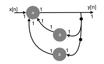
A block diagram is a very simple graphical method that consists of functional blocks connected with directed edges. A connected edge represents flow of data from source block to destination block. Figure 4.14. shows a block diagram representation of a 3-coefficients FIR filter implementing this equation:
In the figure, the functional blocks are drawn to represent multiplication, addition and delay operations. These blocks are connected by directed edges showing the precedence of operations and data flow in the architecture. It is important to note that the DSP algorithms are iterative. Each iteration of the algorithm implements a series of tasks in a specific order. A delay element stores the intermediate result produced by its source node. This result is used by the destination node on the same edge in the next iteration of the algorithm. Figure 4.15. shows source node U performing
Figure 4.13 Graphical representation of a signal processing algorithm where node P3 is described in RTL and optimized assembly targeting an FPGA or a particular DSP respectively
Figure 4.14 Dataflow graph representation of a 3-coefficient FIR filter
Figure 4.15 Source and destination nodes with a delay element on the joining edge
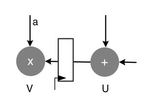
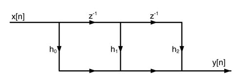
Figure 4.16 Signal flow graph representation of a 3-coefficient FIR filter
the addition operation and storing the value in the register on the edge, whereas the node V uses the stored value of the last iteration in the register for its multiplication by a constant a.
4.5.3 Signal Flow Graph
A signal flow graph (SFG) is a simplified version of a block diagram. The operation of multiplication with a constant and delays are represented by edges, whereas nodes represent addition, subtraction and input and output (I/O) operations.
Figure 4.16 shows an SFG implementation of equation (4.1) above. The edges with h0, h1 and h2 represent multiplication of the signal at the input of the edges by respective constants, z-1 on the arrow represents a delay element, the node where two arrows meet shows the addition operation, and a node with one incoming and two outgoing edges means that the data on the input edge is broadcast to output edges.
SFGs are primarily used in describing DSP algorithms. Their use in representing architectures is not very attractive.
4.5.4 Dataflow Graph or Data Dependency Graph
In a DFG representation, a signal processing algorithm is described by a directed graph G = ,<V, E>, where a node v ∈ V represents a computational unit or, in a hierarchical design, a sub-graph already described subscribing to the rules of DFG. A directed edge e ∈ E from a source node to a destination node represents either a FIFO buffer or just precedence of execution. It is also used to represent algorithmic delays introduced to data while it moves from source node to destination node. A destination node can fire only if it has on all its input edges the predefined number of tokens. Once a node executes, it consumes the defined number of tokens from its input edges and generates a defined number of tokens on all its output edges.
A DFG representation is of special interest to hardware designers as it captures the data-driven property of a DSP algorithm. A DFG representation of a DSP algorithm exposes the hidden concurrency among different parts of the algorithm. This concurrency then can be exploited for parallel mapping of the algorithm in HW. A DFG can be used to represent synchronous, asynchronous and multi-rate DSP algorithms. For an asynchronous algorithm, an edge ‘e’ represents a FIFO buffer.
DFG representation is very effective in designing and synthesizing DSP systems. It motivates the designer to think in terms of components. A component-based design, if defined carefully, helps in reuse of the components in other design instances. It also helps in module-level optimization, testing and verification. The system can be easily profiled and the profiling results along with the structure of the DFG facilitate HW/SW partitioning and subsequent co-design, co-simulation and co-verification.
Figure 4.17 Hypothetical DFG with three nodes and three edges
Each node in the graph may represent an atomic operation like multiplication, addition or subtraction. Alternatively, each node may coarsely define a computational block such as FIR filter, IIR filter or FFT. In these design instances, a predesigned library for each node may already exist. The designer needs to exactly compute the throughput for each node and the storage requirement on each edge. While mapping a cascade of these nodes to HW, a controller can be easily designed or automatically generated that synchronizes the operation of parallel implementation of these nodes.
A hypothetical DFG is shown in Figure 4.17, where each node represents a computational block defined at coarse granularity and edges represent connectivity and precedence of operation. For HW mapping, appropriate HW blocks from a predesigned library are selected or specifically designed with a controller synchronizing the nodes to work in lock step for parallel or sequential implementation.
Figure 4.18 shows the scope of different sub-classes of graphical representations. These representations are described in below sections. The designer needs to select, out of all these representations, an appropriate representation to describe the signal processing algorithm under consideration. The KPN is the most generalized representation and can be used for implementing a wide range of signal processing systems. In many design instances, the algorithm can be defined more precisely at a finer level with details of number of cycles each node takes to execute its computation and the number of tokens it consumes at firing, and as a result the number of tokens it produces at its output edges. These designs can be represented using cyclo-static DFG (CSDFG), synchronous DFG (SDFG) and homogenous SDFG (HSDFG) – in reducing order of generality.
Figure 4.18 Scope of different subclasses of graphical representation, moving inward from the most generalized KPN to dynamic DFG (DDFG), to CSDFG, to SDFG, and ending at the most constrained HSDFG
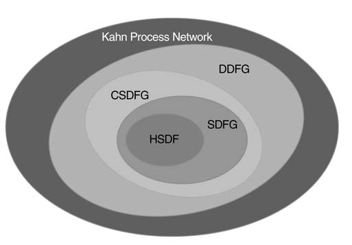
Figure 4.19 SDFG with nodes S and D
When the number of cycles each node takes to execute and the number of tokens produced and consumed by the node are not known a priori, these design cases can be modeled as dynamic DFG (DDFG).
4.5.4.1 Synchronous Dataflow Graph
A typical streaming application continuously processes sampled data from an A/D converter and the processed data is sent to a D/A converter. An example of a streaming application is a multimedia processing system consisting of processes or tasks where each task operates on a predefined number of samples and then produces a fixed number of output values. These tasks are periodically executed in a defined order.
A synchronous dataflow graph (SDFG) best describes these applications. Here the number of tokens consumed by a node on each of its edges, and as a result of its firing the number of tokens it produces on its output edges, are known a priori . This leads to efficient HW mapping and implementation.
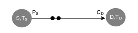
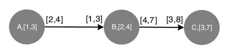
Nodes are labeled with their names and number of cycles or time units they take in execution, as demonstrated in Figure 4.19. An edge is labeled at tail and head with production and consumption rates, respectively. The black dots on the edges are the algorithm delays between two nodes. Figure 4.19 shows source and destination nodes S and D taking execution time TS and TD units, respectively. The data or token production rate of S is PS and the data consumption rate of node D is CD. The edge shows two algorithmic delays between the nodes specifying that node D uses two iterations-old data for its firing.
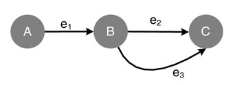
An example of an SDFG is shown in Figure 4.20(a). The graph consists of three nodes A, B and C with execution times of 2, 1 and 1 time units, respectively. The production and consumption rates of each node are also shown, with the number of required initial delays represented by filled circles on the edges.
An SDFG can also be represented by a topology matrix , as shown in Figure 4.20(b). Each column of the matrix represents a node and each row corresponds to an edge. The three columns represent nodes A, B and C in the same order. The first row depicts edge e1 connecting nodes A and B. Similarly the second and third rows show the connections on edges e2 and e3 , respectively.
Figure 4.20 (a) Example of an SDFG with three nodes A, B and C. (b) Topology matrix for the SDFG
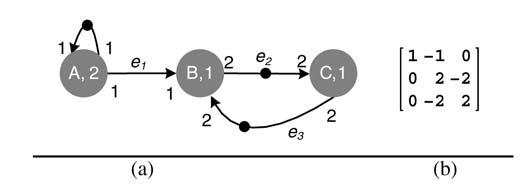
Figure 4.21 SDFG implementing the difference equation (4.2)
The production and consumption rates are represented by positive and negative numbers, respectively.
4.5.4.2 Example: IIR Filter as an SDFG
Draw an SDFG to implement the difference equation below:
The SDFG modeling the equation is given in Figure 4.21. The graph consists of two nodes for multiplications and one node for addition, each taking one token as input and producing one token at the output. The feedback paths from the output to the two multipliers each requires a delay. These delays are shown with black dots on the respective edges.
4.5.4.3 Consistent and Inconsistent SDFG
An SDFG is described as consistent if it is correctly constructed. A consistent SDFG, once it executes, neither starves for data nor requires any unbounded FIFOs on its edges. These graphs represent both single- and multiple-rate systems. The consistency of an SDFG can be easily confirmed by computing the rank of its topology matrix and checking whether that is one less than the number of nodes in the graph [24].
An SDFG is described as inconsistent and experiences a deadlock in a streaming application if some of its nodes starve for data at its input to fire, or on some of its edges it may need unbounded FIFOs to store an unbounded production of tokens.
4.5.4.4 Balanced Firing Equations
A node in an SDFG fires a number of times, and in every firing produces a number of tokens on its outgoing edges. All the nodes connected to this node on these direct edges must consume all the tokens in their respective firing. Let nodes S and D be directly connected as shown in Figure 4.19, where node S produces PS tokens and node D consumes CD tokens in their respective firings. A balanced firing relationship can be expressed as:
Figure 4.22 Examples of inconsistent DFGs resulting in only the trivial solution of a set of balanced-firing equations where no node fires. (a) DFG requires unbounded FIFOs. (b) Node A will starve for data as it requires three tokens to fire and only gets one from node B
where fS and fD are non-zero finite minimum positive values. This definition can be hierarchically extended for an SDFG with N nodes, where node 1 is the input and node N is the output:
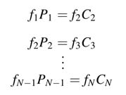
The values f1 ... fN form a vector called the repetition vector . It can be observed that this vector is obtained by computing a non-trivial solution to the set of equations given in (4.4). The repetition vector requires each node to fire fi times. This makes all the nodes in an SDFG fire synchronously, producing enough tokens for the destination nodes and consuming all the data values being produced by its source nodes.
A set of balanced equations for an SDFG greatly helps a digital designer to design logic in each node such that each node takes an equal number of cycles for its respective firing. The concept of balanced equations and their effective utilization in digital design is illustrated later in this chapter. It is pertinent to note that there are design instances where a cyclo-static schedule is required where a node may take different time units and generate a different number of tokens in each of its firings and then periodically repeat the pattern of firing.
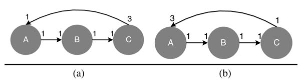
Example: Find a solution of balanced equations for the SDFG given in Figure 4.22(a). The respective balanced equations for the links A → B, B → C and C → A are:
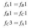
No non-trivial solution exists for these set of equations as the DFG is inconsistent.
4.5.4.5 Consistent and Inconsistent SDFGs
If no non-trivial solution with non-zero positive values exists for the set of balanced firing equations, then it is inferred that the DFG is an inconsistent SDFG. This is equivalent to the check on the rank of the topology matrix T, as any set of balanced equations for an SDFG can be written as:
where f = [f1, f2, ... fN ] is the repetition vector for a graph with N nodes.
Solving a set of three equations given by (4.5) for example in Figure 4.22(a) only yields a non-trivial solution. It is also obvious from the DFG that node C produces three tokens, and node A, in the second iteration, consumes them in three subsequent firings. As a result, node B and C also fire three times and C produces nine tokens. In each iteration, C fires three times its previous number of firings. Thus this DFG requires unbounded FIFOs and shows an algorithmic inconsistence in the design. Using the balanced firing relationship of (4.3), produce/consume equations for links A →B, B → C and C → A are written as:
(4.6)
The only solution for the set of equations is the trivial fA =fB =fC =0. Another equally relevant case is shown in Figure 4.22(b) where, following the sequential firing of different nodes, node A will starve for data in the second iteration as it requires three tokens for its firing and will only get one from node B.
4.5.5 Self-timed Firing
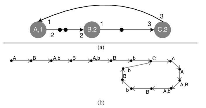
In a self-timed firing, a node fires as soon as it gets the requisite number of tokens on its incoming edges. For implementing SDFG on dedicated hardware, either self-timed execution of nodes can be used or a repetition vector can be first calculated using a balanced set of equations. This vector calculates multiple firings of each node to make the SDFG consistent. This obviously requires a larger buffer size at the output of each edge to accumulate tokens resulting from multiple firing of a node. A self-timed SDFG implementation usually results in a transient phase, and after that the firing sequence repeats itself in a periodic phase. Self-timed SDFG implementation requires minimum buffer sizes as a node fires as soon as the buffers on its inputs have the requisite number of samples.
Example: Figure 4.23(a) shows an SDFG with three nodes, A, B and C, having execution time of 1, 2 and 2 time units, respectively. The consumption and production rates for each link are also shown. In a self-timed configuration, an implementation goes through a transient phase where nodes A and B fire three times to accumulate three token at the input of C. Node B takes two time units to complete its execution. In Figure 4.23(b) the first time unit is shown with capital letter ‘B’ and the second time unit is shown with small letter ‘b’. This initial firing brings the self-timed implementation in periodic phase where C fires and generates three tokens at its output. This makes A fire three times, and so does B, generating three tokens at input of C – and the process is repeated in a periodic fashion.
4.5.6 Single-rate and Multi-rate SDFGs
In a Single-Rate SDFG, the consumption rate rc (the number of tokens consumed on each incoming edge) is same as the production rate rp (the number of tokens produced at the outgoing edges). In a Multi-Rate SDFG, these rates are not equal and one is a rational multiple of the other. For a decimation multi-rate system, rc > rp . An interpolation system observes a reverse relationship, rp < rc .
Figure 4.23 Example of self-timed firing where a node fires as soon as it has enough tokens on its input. (a) An SDFG. (b) Firing pattern using self-timed firing
An algorithm described as a synchronous DFG makes it very convenient for a designer or an automation tool to synthesize the graph and generate SW or HW code for the design. This representation also helps the designer or the tools to apply different transformations on the graph to make it optimized for a set of design constraints and objective functions. The representation can also be directly mapped on dedicated HW, or time-multiplexed HW. For time-multiplexed HW, several techniques have been evolved to generate an optimal schedule and HW architecture for the design. Time-multiplexed architectures are covered in Chapters 8 and 9.
Example: A good example of a multi-rate DFG is a format converter to store a CD-quality audio sampled at 44.1 kHz to a digital audio tape (DAT) that records a signal sampled at 48kHz. The following is the detailed workout of the format conversion stages [25]:
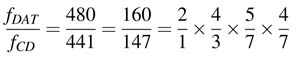
The first stage of rate change is implemented as an interpolator by 2, and each subsequent stage is implemented as a sampling rate change node by a rational factor P/Q , where P and Q are interpolation and decimation factors. This sampling rate change is implemented by an interpolation by a factor of P, and then passing the interpolated signal through a low-pass FIR filter with cutoff frequency π/max (P,Q). The signal from the filter is decimated by a factor of Q [9].
Figure 4.24 shows the SDFG that implements the format converter. The SDFG consists of processing nodes A, B, C and D implementing sampling rate conversion by factors of 2/1, 4/3, 5/7 and 4/7, respectively. In the figure CD and DAT represent source and destination nodes.
Figure 4.24 SDFG implementing CD to DAT format converter
There are two simple techniques to implement the SDFG for the format conversion. One method is to first compute the repetition vector by first generating the set of produce/consume equations for all edges and then solving it for a non-trivial solution with minimum positive values. The solution turns out to be [147 98 56 40] for firing of nodes A, B, C and D, respectively. Although this firing is very easy to schedule, it results in an inefficient requirement on buffer sizes. For this example the implementation requires multiple buffers of sizes 147, 147 × 2, 98 × 4, 56 × 5 and 40 × 4 on edges moving from source to destination, accumulating a total storage requirement of 1273 samples.
The second design option is for each node to fire as soon as it gets enough samples at its input port. This implementation will require multiple buffers of sizes 1,4,10,11 and 4 on respective edges from source to destination, amounting to a total buffer size of 30 words.
4.5.7 Homogeneous SDFG
Homogeneous SDFG is a special case of a single-rate graph where each node produces one token or data value on all its outgoing edges. Extending this account to incoming edges, each node also consumes one data value from all its incoming edges. Any consistent SDFG can be converted into HSDFG. The conversion gives an exact measure of throughput, athough the conversion may result in an exponential increase in the number of nodes and thus may be very complex for interpretation and implementation.
The simplest way to convert a consistent SDFG to HSDFG is to first find the repetition vector and then to make copies of each node as given in the repetition vector and appropriately draw edges from source nodes to the destination nodes according to the original SDFG.
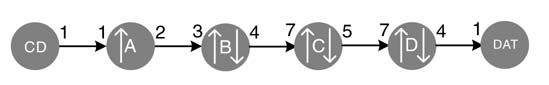
Example: Convert the SDFG given in Figure 4.25(a) to its equivalent HSDFG. This requires first finding the repetition vector from a set of produce/consume equations for the DFG. The repetition vector turns out to be [2 4 3] for set [A B C]. The equivalent HSDFG is drawn by following the repetition vector where nodes A, B and C are drawn 2,4 and 3 times, respectively. The parallel nodes are then connected according to the original DFG. The equivalent HSDFG is given in Figure 4.25(b).
Example: Section 4.4.2.1 considered a JPEG realization as a KPN network. It is interesting to observe that each process in the KPN can be described as a dataflow graph. Implementation of a two-dimensional DCT block is given here. There are several area-efficient algorithms for realizing a 2-D DCT in hardware [26-29], but let us consider the simplest algorithm that computes 2-D DCT by successively computing two 1-D DCTs while performing transpose before the first DCT computation. This obviously is a multi-rate DFG, as shown in Figure 4.26.
The first node in the DFG takes 64 samples as an 8×8 block B, and after performing transpose of the input block it produces 64 samples at the output. The next node computes a 1-D DCT Ci of each of the rows of the block, MATLAB® notation BT(i,:) is used to represent each row i (= 0,…, 7) of block BT. This node, in each of its firings, takes a row comprising 8 samples and computes 8 samples at the output. The next FIFO at the output keeps collecting these rows, and the next node fires only when all 8 rows consisting of 64 elements of C are computed and saved in the FIFO. This node computes the transpose of C. In the same manner the next node computes 8 samples of the one-dimensional DCT Fj of each column j of CT.
This DFG can be easily converted into HSDFG by replicating the 1-D DCT computation 8 times in both the DCT computation nodes.
4.5.8 Cyclo-static DFG
In a cyclo-static DFG, the number of tokens consumed by each node, although varying from iteration to iteration, exhibits periodicity and repeats the pattern after a fixed number of iterations. A CS-DFG
Figure 4.25 SDFG to HSDF conversion. (a) SDFG consisting of three nodes A, B and C. (b) An equivalent HSDG
is more generic and is suited to modeling several signal processing applications because it provides flexibility of varying production and consumption rates of each node provided the pattern is repeated after some finite number of iterations. This representation also works well for designs where a periodic sequence of functions is mapped on same HW block. Modeling it as CS-DFG, a node, in a periodic pattern, fires and executes a different function in a sequence and then repeats the sequence of calls after a fixed number of function calls. Each function observes different production and consumption rates, so the number of tokens in each firing of a node is different.
Figure 4.27 showsaCS-DFG where nodesA, B andC each executes two functions with execution times of [1, 3], [2, 4] and [3, 7] time units, respectively. In each of their firings the nodes produce and consume different numbers of tokens. This is shown in the figure on respective edges.
To generalize the execution in a CS-DFG node, in a periodic sequence of calls with period N, an iteration executes a function out of a sequence of functions f0 (.),... f(N–1). Other nodes also call functions in a sequence. Each call consumes and produces a different number of tokens.
Figure 4.26 Computing a two-dimensional DCT in a JPEG algorithm presents a good example to demonstrate a multi-rate DFG
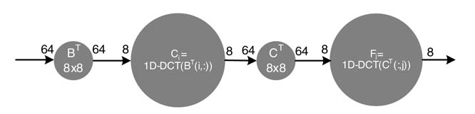
Figure 4.27 Example of a CSDFG, where node A first fires and takes 1 time unit and produces 2 tokens, and then in its second firing it takes 3 time units and generates 4 tokens. Node B in its first firing consumes 1 token in 2 time unit, and the in its second firing takes 4 time units and consumes 3 tokens; it respectively produces 4 and 7 tokens. A similar behavior of node C can be inferred from the figure
4.5.9 Multi-dimensional Arrayed Dataflow Graphs
This graph consists of an array of nodes and edges. The graph works well for multi-dimensional signal processing or parallel processing algorithms.
4.5.10 Control Flow Graphs
Although a synchronous dataflow graph (SDFG) is statically schedulable owing to it predictable communications, it can also express recursion with a fixed number of iterations. However, the representation has an expressive limitation because it cannot capture a data-dependent flow of tokens unless it makes use of transition refinements. This limitation prevents a concise representation of conditional flows incorporating if-else-then and do-while loops and data-dependent recursions.
As opposed to a DFG which is specific to a dataflow algorithm, a CFG is suitable to process a control algorithm. These algorithms are usually encountered in implementing communication protocols or controller designs for datapaths.
A control dataflow graph (CDFG) combines data-driven and control-specific functionality of an algorithm. Each node of the DFG represents a mathematical operation, and each edge represents either precedence or a data dependency between the operations. A CDFG may change the number of tokens produced and consumed by the nodes in different input settings. A DFG with varying rates of production and consumption is called a dynamic dataflow graph (DDFG).
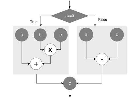
Example: The example here converts a code consisting of decision statements to CDFG. Figure 4.28 shows a CDFG that implements the following code:
if (a= =0)
 c=a+bxe;
else
 c=a-b;
The figure shows two conditional edges and two hierarchically built nodes for conditional firing. This type of DFG is transformed for optimal HW mapping by exploiting the fact that only one of the many conditional nodes will fire. The transformed DFG shares a maximum of HW resources and moves the conditional execution on selection of operands for the shared resource.
A dataflow graph is a good representation for reconfigurable computing. Each block in the DFG can be sequentially mapped on reconfigurable hardware. Figure 4.29 illustrates the fact that, in a JPEG implementation, sequential firing of nodes can be mapped on the same HW. This sharing of HW resources at run time reduces the area required, at the cost of longer execution times.
Figure 4.28 CDFG implementing conditional firing
4.5.11 Finite State Machine
A finite state machine (FSM) is used to provide control signals to a signal processing datapath for executing a computation with a selection of operands from a set of operands. An FSM is useful once a DFG is folded and mapped on a reduced HW, thus requiring a scheduler to schedule multiple nodes of the graph on a HW unit in time-multiplexed fashion. An FSM implements a scheduler in these designs.
A generic FSM assumes a system to be in one of a finite number of states. An FSM has a current state and, based on an internal or external event, it then computes the next state. The FSM then transitions into the next state. In each state, usually the datapath of the system executes a part of the algorithm. In this way, once the FSM transits from one state to another, the datapath keeps implementing different portions of the algorithm. After finishing the current iteration of the algorithm, the FSM sets its state to an initial value, and the datapath starts executing the algorithm again on a new set of data.
Figure 4.29 A dataflow graph is a good representation for mapping on a run-time reconfigurable platform
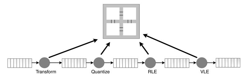
Figure 4.30 Mathematical transformation changing a DFG to meet design goals
Besides implementing a scheduler, the FSM also works well to implement protocols where a set of procedures and synchronization is followed among various components of the system, as with shared-bus arbitration. Further treatment to the subject of FSM is given in Chapter 9.
4.5.12 Transformations on a Dataflow Graph
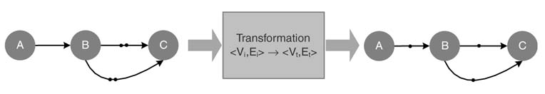
Mathematical transformations convert a DFG to a more appropriate DFG for hardware implementation. These transformations change the implementation of the algorithm such that the transformed algorithm better meets specific goals of the design. Out of a set of design goals the designer may want to minimize critical path delay or the number of registers. To achieve this, several transformations can be applied to a DFG. Retiming, folding, unfolding and look-ahead are some of the transformations commonly used. These are covered in Chapter 7.
A transformation as shown in Figure 4.30 takes the current representation of DFGi= <Vi, Ei> and translates it to another DFGt= <Vt, Et> with the same functionality and analytical behavior but different implementation.
4.5.13 Dataflow Interchange Format (DIF) Language
Dataflow interchange format is a standard language for specifying DSP systems in terms of executable graphs. Representation of an algorithm in DIF textually captures the execution model. An algorithm defined in DIF format is extensible and can be ported across platforms for simulation and for high-level synthesis and code generation. More information on DIF is given in [25].
4.6 Performance Measures
A DSP implementation is subject to various performance measures. These are important for comparing design tradeoffs.
4.6.1 Iteration Period
For a single-rate signal processing system, an iteration of the algorithm acquires a sample from an A/D converter and performs a set of operations to produce a corresponding output sample. The computation of this output sample may depend on current and previous input samples, and in a recursive system the earlier output samples are also used in this calculation. The time it takes the system to compute all the operations in one iteration of an algorithm is called the iteration period. It is measured in time units or in number of cycles.
For a generic digital system, the relationship between the sampling frequency fs and the circuit clock frequency fc is important. When these are equal, the iteration period is determined by the critical path. In designs where fc > fs , the iteration period is measured in terms of the number of clock cycles required to compute one output sample. This definition can be trivially extended for multi-rate systems.
4.6.2 Sampling Period and Throughput
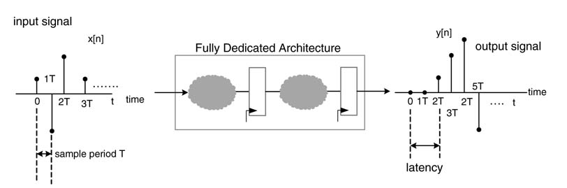
The sampling period Ts is defined as the average time between two successive data samples. The period specifies the number of samples per second of any signal. The sampling rate or frequency (fs = 1/Ts ) requirement is specific to an application and subsequently constrains the designer to produce hardware that can process the data that is input to the system at this rate. Often this constraint requires the designer to minimize critical path delays. They can be reduced by using more optimized computational units or by adding pipelining delays in the logic (see later). The pipelining delays add latency in the design. In designs where fs <fc , the digital designer explores avenues of resource sharing for optimal reuse of computational blocks.
4.6.3 Latency
Latency is defined as the time delay for the algorithm to produce an output y [n ] in response to an input x[n ]. In many applications the data is processed in batches. First the data is acquired in a buffer and then it is input for processing. This acquisition of data adds further latency in producing corresponding outputs for a given set of inputs.
Beside algorithmic delays, pipelining registers (see later) are the main source of latency in an FDA. In DSP applications, minimization of the critical path is usually considered to be more important than reducing latency. There is usually an inverse relationship between critical path and latency. In order to reduce the critical path, pipelining registers are added that result in an increase in latency of the design. Reducing a critical path helps in meeting the sampling requirement of a design.
Figure 4.31 shows the sampling period as the time difference between the arrivals of two successive samples, and latency as the time for the HW to produce a result y [n ] in response to input x [n ].
Figure 4.31 Latency and sampling period
4.6.4 Power Dissipation
4.6.4.1 Power
Power is another critical performance parameter in digital design. The subject of designing for low power use is gaining more importance with the trend towards more handheld computing platforms as consumer devices.
There are two classes of power dissipation in a digital circuit, static and dynamic. Static power dissipation is due to the leakage current in digital logic, while dynamic power dissipation is due to all the switching activity. It is the dynamic power that constitutes the major portion of power dissipation in a design. Dynamic power dissipation is design-specific whereas static power dissipation depends on technology.
In an FPGA, the static power dissipation is due to the leakage current through reversed-biased diodes. On the same FPGA, the use of dynamic power depends on the clock frequency, the supply voltage, switching activity, and resource utilization. For example, the dynamic power consumption Pd in a CMOS circuit is:
![]()
where α and C are, respectively, switching activity and physical capacitance of the design, VDD is the supply voltage and f is the clock frequency. Power is a major design consideration especially for battery-operated devices.
At register transfer level (RTL), the designer can determine the portions of the design that are not performing useful computations and can be shut down for power saving. A technique called ‘gated clock’ [30–32] is used to selectively stop the clock in areas that are not performing computations in the current cycle. A detailed description is given in Chapter 9.
4.7 Fully Dedicated Architecture
4.7.1 The Design Space
To design an optimal logic for a given problem, the designer explores the design space where several options are available for mapping real-time algorithms in hardware. The maximum achievable clock frequency of the circuit, fc , and the required sampling rate of data input to the system, fs , play crucial roles in determining and selecting the best option.
Digital devices like FPGAs and custom ASICs can execute the logic at clock rates in the range of 30 MHz to at least 600 MHz. Digital front end of a software defined radio (SDR) requires sampling and processing of an IF signal centered at 70 MHz. The signal is sampled at between 150 and 200 MHz. For this type of application it is more convenient to clock the logic at the sampling frequency of the A/D converter or the data input rate to the system. For these designs not many options are available to the designer, because to process the input data in real time each operation of the algorithm requires a physical HW operator. Each operation in the algorithm – addition, multiplication and algorithmic delay – requires an associated HW unit of adder, multiplier and register, respectively. Although the designer is constrained to apply one-to-one mapping, there is flexibility in the selection of an appropriate architecture for basic HW operators. For example, for simple addition, an adder can be designed using various techniques: ripple carry, carry save, conditional sum, carry skip, carry propagate, and so on. The same applies to multipliers and shifters, where different architectures are being designed to perform these basic operations. The design options for these basic mathematical operations are discussed in Chapter 5. These options usually trade off area against timing.
Figure 4.32 Mapping to a dataflow graph of the set of equations given in the text example
After one-to-one mapping of the DFG to architecture, the design is evaluated to meet the input data rate of the system. There will be cases where, even after selecting the optimal architectures for basic operations, the synthesized design does not meet timing requirements. The designer then needs to employ appropriate mathematical transformations or may add pipeline registers to get better timing (see later).
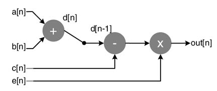
Example: Convert the following statements to DFG and then map it to fully dedicated architecture.
This is a very simple set of equations requiring addition, a delay element, a subtraction and a multiplication. The index n represents the current iteration, and n – 1 represents the result from the previous iteration. The conversion of these equations to a synchronous DFG is shown in Figure 4.32.
After conversion of an algorithm to DFG, the designer may apply mathematical transformations like retiming and unfolding to get a DFG that better suits HW mapping. Mapping of the transformed DFG to architecture is the next task. For an FDA the conversion to an initial architecture is very trivial, involving only replacement of nodes with appropriate basic HW building blocks.
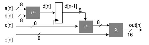
Figure 4.33 shows the initial architecture mapping of the DFG of (4.7) and (4.8). The operations of the nodes are mapped to HW building blocks of an adder, subtractor, multiplier and a register.
4.7.2 Pipelining
Mapping of a transformed dataflow graph to fully dedicated architecture is trivial, because each operation is mapped to its matching hardware operator. In many cases this mapping may consist of paths with combinational logic that violates timing constraints. It is, therefore, imperative to break these combinational clouds with registers. Retiming transformation, which is discussed in Chapter 7, can also be used for effectively moving algorithmic registers in the combinational logic that violates timing constraints.
Figure 4.33 DFG to FDA mapping
For feedforward paths, the designer also has the option to add additional pipeline registers in the path. As the first step, a DFG is drawn from the code and, for each node in the graph, an appropriate HW building block is selected. Where there is more than one option of a basic building block, selecting an appropriate HW block becomes an optimization problem. After choosing appropriate basic building blocks, these are then connected in the order specified by the DFG. After this initial mapping, timing of the combinational clouds is computed. Based on the desired clock rate, the combinational logic may require retiming of algorithmic registers; or, in case of feedforward paths, the designer may need to insert additional pipeline registers.
Figure 4.34 shows the steps in mapping a DFG to fully dedicated architecture while exercising the pipelining option for better timing.
Maintaining coherency of the data in the graph is a critical issue in pipelining. The designer needs to make sure that the datapath traced from any primary input to any primary output passes through the same number of pipeline registers. Figure 4.35 shows that to partition the combinational cloud of
Figure 4.34 Steps in mapping DFG on to FDA with pipeline registers
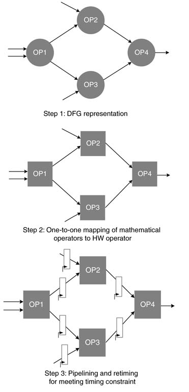
Figure 4.35 Pipelining while maintaining coherency in the datapath
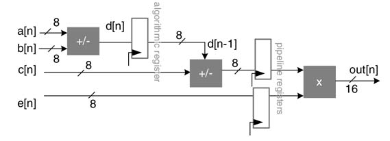
Figure 4.33, a pipeline register needs to be inserted between the multiplier and the subtractor; but, to maintain coherency of input e [n ] to the multiplier, one register is also added in the path of the input e [n ] to the multiplier.
When some of the feedforward paths of the mapped HW do not meet timings, the designer can add pipeline registers to these paths. In contrast, there is no simple way of adding pipeline registers in feedback paths. The designer should mark any feedback paths in the design because these require special treatment for addition of any pipeline registers. These special transformations are discussed in Chapter 7.
4.7.3 Selecting Basic Building Blocks
As an example, a dataflow graph representing a signal processing algorithm is given in Figure 4.36(a). Let there be three different types of multiplier and adder in the library of predesigned basic building blocks. The relative timing and area of each building block is given in Table 4.1. This example designs an optimal architecture with minimum area and best timing while mapping the DFG to fully dedicated architecture.
Figure 4.36 One-to-one mathematical operations. (a) Dataflow graph. (b) Fully dedicated architecture with optimal selection of HW blocks
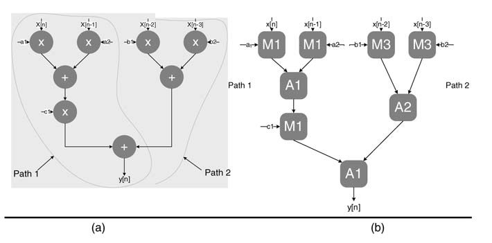
Table 4.1 Relative timings and areas for basic building blocks used in the text example
| Basic building blocks | Relative timing | Relative area |
| Adder 1 (A1) | T | 2.0A |
| Adder 2 (A2) | 1.3T | 1.7A |
| Adder 3 (A3) | 1.8T | 1.3A |
| Multiplier 1 (M1) | 1.5T | 2.5A |
| Multiplier 2 (M2) | 2.0T | 2.0A |
| Multiplier 3 (M3) | 2.4T | 1.7A |
The DFG of Figure 4.36(a) is optimally mapped to architecture in(b). The objective is to clock the design with the best possible sampling rate without addition of any pipeline register. The optimal design selects appropriate basic building blocks from the library to minimize timing issues and area.
There are two distinct sections in the DFG. The critical section requires the fastest building blocks for multiplications and additions. For the second sections, first the blocks with minimum area should be allocated. If any path results in a timing violation, an appropriate building block with better timing while still smaller area should be used to improve the timing. For complex designs the mapping problem can be modeled as an optimization problem and can be solved for an optimal solution.
4.7.4 Extending the Concept of One-to-one Mapping
The concept can be extended to graphs that are hierarchically built where each node implements an algorithm such as FIR or FFT. Then there are also several design options to realize these algorithms. These options are characterized with parameters of power, area, delay, throughput and so on. Now what is needed is a design tool that can iteratively evaluates the design by mapping different design options and then settling for the one that best suits the design objectives. A system design tool to work in this paradigm needs to develop different design options for each component offline and to place them in the design library.
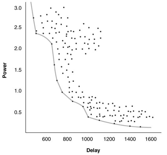
Figure 4.37 demonstrates what is involved. The dots in the figure show different design instances and the solid line shows the tradeoff boundary limiting the design space exploration. The user defines a delay value and then chooses an architecture in the design space that best suits the objectives while minimizing the power.
4.8 DFG to HW Synthesis
A dataflow graph provides a comprehensive visual representation to signal processing algorithms. Each node is characterized by production and consumption rates of tokens at each port. In many instances, several options for a component represented as a node in the DFG exists in the design library. These components trade off area with the execution time or number of cycles it takes to process the input tokens.
In this section we assume that a design option for implementing a node has already been made. The section presents a technique for automatic mapping and interworking of nodes of a DFG in hardware. This mapping requires convertion of the specifications for each edge of the DFG to appropriate HW, and generation of a scheduler that synchronizes the firings of different nodes in the DFG [33].
Figure 4.37 ower–delay tradeoff for a typical digital design
4.8.1 Mapping a Multi-rate DFG in Hardware
Each edge is considered with its rates of production and consumption of tokens. For an edge requiring multi-rate production to single-rate consumption, either a parallel or a sequential implementation is possible. A parallel implementation invokes each destination node multiple times, whereas a sequential setting stores the data in registers and sequentially inputs it to a single destination node.
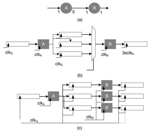
For example, Figure 4.38(a) shows an edge connecting nodes A and B with production and consumption rates of 3 and 1, respectively. The edge is mapped to fully parallel and sequential designs where nodes are realized as HW components. The designs are shown in Figures 4.38(b) and (c).
4.8.1.1 Sequential Mapping
The input to component A is fed at the positive edge of clkG, whereas component B is fed with the data at three times faster clock speed. Based on the HW implementation, A and B can execute at independently running clocks clkA and clkB. In design instances where a node implements a complete functionality of an algorithm, these clocks are much faster than clkG. There may be design instances where, in a hierarchical fashion, each node also represents a DFG and the graph is mapped on fully dedicated architecture. Then clkA and clkB are set to be clkG and 3 ×clkG, respectively.
Figure 4.38(a) Multi-rate to single-rate edge. (b) Sequential synthesis. (c) Parallel synthesis
4.8.1.2 Parallel Mapping
A parallel realization uses the same clock for both the inputs to components A and B as shown in Figure 4.38(c). Further to this, if the design is also mapped as FDA then the entire design would run on global clk G.
In a multi-rate system where the consumption and production rates are different, the buffering design becomes more complex. This requires either a self-timed implementation or balanced-equation based multiple firing realizations. In a self-timed implementation, the firing of the destination node may happen a variable number of times in a period.
Example: Figure 4.39(a) shows a multi-rate edge with rate of production and consumption 3 and 4, respectively. Every time a source node fires it produces three tokens of N bits each, and writes them in a ping-pong pattern in two sets of three registers, {R1, R2, R3} and {R4, R5, R6}. The destination node B consumes the produced tokens in a firing sequence in relation to the firing of node A as [0 111]. Node A fires in the first cycle and stores the output values in registers {R1, R2, R3}. In the second cycle node B does not fire as it requires four tokens, but node A fires again and three new tokens are produced in registers {R4, R5, R6}. As the total number of tokens produced becomes six, so B fires and consumes four tokens in {R1, R2, R3, R4}. Node A also fires in this cycle and again saves the three tokens in registers {R1, R2, R3}, and total number of unconsumed tokens becomes five. In sequential firing, the node B fires again and consumes tokens in registers {R5, R6, R1, R2}, and A also fires and stores tokens in {R4, R5, R6}. The unconsumed tokens are four now, so B fires again and consumes four tokens in registers {R3, R4, R5, R6}. This pattern is repeated thereafter. Figure 4.39(b) shows the HW design that supports this production and consumption of tokens.
Figure 4.39 (a) A multi-rate DFG. (b) Hardware realization
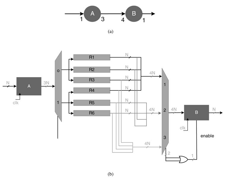
4.8.2 Centralized Controller for DFG Realization
Chapter 9 is dedicated to state-machine based controller design, but in this section a brief introduction to a centralized controller for a DFG realization in HW is given. Several automation tools use a similar methodology to add a controller while generating a HW design for a DFG [33, 34].
The first step in implementing a central controller for a DFG is to classify all the nodes in the DFG as one of the following: a combination node, or a sequential node that executes and generates an output in every sample clock cycle, oranode that executes and generates output tokens in predefined number of circuit clock cycles, or a node that takes a variable number of circuit clock cycles to complete its execution. A sample clock cycle is the clock that latches a new sample into the logic, whereas a circuit clock is usually much faster than a sample clock and executes sequential logic in each node.
An automation tool either picks an appropriate implementation of a node from a design library or produces HDL code using a code-generation utility. A node containing combinational logic or sequential logic executing on the sample clock does not require any control signal except a reset signal that must be used to reset any feedback register in the design. A node with predefined number of circuit clock cycles requires a start signal from a controller, whereas a dynamic node gets a start signal from a controller and then, after completing its execution, it generates a done signal to notify the controller for further asserting control signals to subsequent nodes in the DFG.
Figure 4.40 (a) Hypothetical DFG with different types of node. (b) Hardware realization
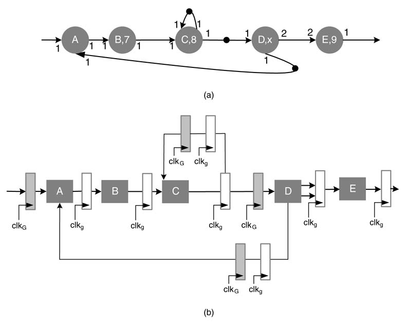
Figure 4.40(a) shows a DFG with nodes A, B, C, D and E. Node A is a combinational logic and nodes B, C and E take 7, 8 and 9 predefined number of circuit clock cycles, respectively. Node D dynamically executes and takes a variable number of cycles. Each black dot shows an algorithmic delay where data from previous iteration is used in subsequent nodes. This dot in actual HW is realized as a register that is clocked by the sampling clock. Now, having the graph and the information about each node, a centralized controller can be easily designed or automatically generated. Such acontroller is shownin Figure 4.40(b). Each node with predefined numberof cycles needs a start signal from the controller, and then the controller counts the number of cycles for the node to complete its execution. The controller then asserts an output enable signal to the register at the output of each such node. In the figure, the output from each node is latched in a register after assertion of an enable signal, whereas the register is clocked by the circuit clock. In the case of the dynamic node D, the controller not only notifies the node to start its execution; the node also after completing its execution asserts a done signal.
For the design in question, a done_D is asserted and the controller then asserts en_out_D to latch the output from node D in a register. The input and output to the DFG and the dots on the edges are replaced by registers clocked by sample clock clk G, whereas the rest of the logic in the nodes and the registers at the output of each node are clocked by a circuit clock clk g. All the feedback register are resetable using a global rst_n signal. It is important to ensure that for a synchronous DFG that implements a streaming application, a new sample to the DFG is fed in every sample clock cycle. The design must be constructed in a manner that all the nodes in the DFG complete their respective executions before the arrival of the next sample clock. Even for the dynamic node, the worst-case condition must be considered and the design must guarantee completion before the arrival of the next sample clock. All the nodes that can do so start and execute in parallel. Nodes A,B and C execute in a sequence, and D and E work in parallel and use the output of C from the previous iteration. If x, the execution of time of dynamic node D, is bounded by 10, then the execution of D and E takes a maximum of 19 circuit clocks, whereas nodes A, B and C take 16 clocks. Thus the circuit clock should be at least 19 times faster than the sampling clock.
Exercises
Exercise 4.1
The code below lists one iteration of an algorithm implementing a block in a digital communications receiver. The algorithm processes a complex input InputSample and gives it a phase correction. The phase correction is computed in this code. Draw DFG, and map it on to an FDA. Write RTL Verilog code of the design using 16-bitfixed point arithmetic. Write a stimulus to verify the RTL code.
>Mixer_out = InputSample*(-j*Phase);
// a number of algorithmic registers
Mixer_Out[2] = Mixer_Out[1];
Mixer_Out[1] = Mixer_Out[0];
Mixer_Out[0] = Mixer_out;
Delayline[2] = Delayline[1];
Delayline[1] = Delayline[0];
// feedback loop, where a and b are arrays of 16-bit constants
// Kp and Ki are also 16-bit constant numbers
Delayline[0]= - Delayline[1]*a[1]
 - Delayline[2]*a[2]
 + Mixer_Out[0]*b[0]
 + Mixer_Out[1]*b[1]
 + Mixer_Out[2]*b[2];
offset = real(Delayline[2]*Delayline[0]);
offset_Delayline[0] = offset_Delayline[1];
offset_Delayline[1] = offset;
phase_corr = Kp*offset_Delayline[0]
 + Ki*offset_Delayline[1]
 + phase_corr
 - Kp*offset_Delayline[1];
Phase = Phase + phase_corr;
Exercise 4.2
Convert the C code shown below to its equivalent fixed-point listing in C. Consider acc to be in Q8.32 format and all the other variables to be Q1.15. Check corner cases and saturate the result if overflow occurs. Draw a DFG of the design and map the DFG as FDA. Write RTL Verilog code of the design. Simulate the design for a stream of input values in Q1.15 format.
float recursion (float input, float x[], float y[])
{
float acc, out;
int i;
acc = 0;
>x[2]=x[1];
x[1]=x[0];
x[0]=input;
for(i = 0; i < 2; i++)
{
acc += b[i] * x[i] + a[i] * y[i];
}
y[2]=y[1];
y[1]=y[0];
y[0]=acc;
}
The constants are:
float b[] = {0.258, -0.309, -0.704};
float a[] = {-0.123, -0.51, 0.223};
Exercise 4.3
Draw an HSDFG to implement a 4-tap FIR filter in transposed direct-form configuration.
Exercise 4.4
Design a sampling-rate converter to translate a signal sampled at 66 MHz to 245 MHz. Compute the buffer requirement if the system is designed to use fixed pattern computation using a repetition vector. Also compute the minimum buffer requirement if the system is implemented to execute on self-timed firing.
Exercise 4.5
Determine balanced equations for the graph shown in Figure 4.41. If the graph is inconsistent, mention the edge and the type of inconsistency and convert the graph to a consistent graph by suggesting modifications of consumption and production rates of any one of the nodes?
Exercise 4.6
Determine balanced equations and compute a non-trivial solution with minimum positive non-zero values for each firing for the SDFG shown inFigure 4.42. Design hardware consisting of registers and multiplexers to implement the graph.
Exercise 4.7
Production and consumption rates in the form of a 2-D array of data are given in Figure 4.43.
Figure 4.41 SDFG for computing balanced equations (exercise 4.5)
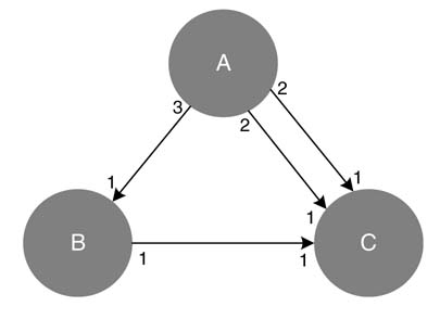
Figure 4.42 SDFG for computing a non-trivial solution (exercise 4.6)
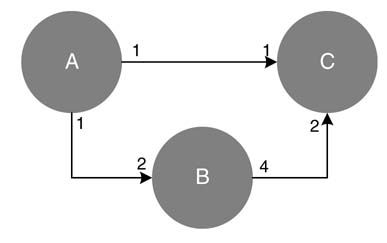
1.Write a balanced equation for both the dimensions. Solve the equation to find a solution to establish the number of firings of B that is required to consume all the tokens produced by A.
2.Draw a 2-D array of data produced by A, and suggest a buffering arrangement with multiplexers to feed the required data to B for its respective firings.
Exercise 4.8
Compute the repetition vector for the SDFG shown in Figure 4.44. Translate the SDFG to HSDFG.
Figure 4.43 Nodes processing a 2-D array of data (exercise 4.7)
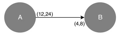
Figure 4.44 SDFG consisting of three nodes (exercise 4.8)
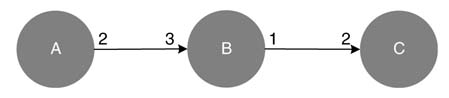
Exercise 4.9
Map the following MATLAB® code to a KPN. Clearly specify the sources, sink and the processing nodes. State the minimum sizes of FIFOs required for implementing the design in hardware.
N = 16;
K = 32;
for i=1:N
 x(i)= src_x ();
end
for j=1:K
 y(j) = src_y ();
end
for i=1:N
 for j=1:K
 x1(i,j)=func1(x(i),y(j));
 y1(i,j)=func2(x(i),y(j));
 end
end
for i=1:N
 for j=1:K
 z(i,j)=func3(x1(i,j),y1(i,j));
 end
end
m=1;
 for i=1:N
 for j=1:K>
 y(m)=sink(x1 (i,j), y1(i,j), z(i,j));
 m=m+1;
 end
end
Exercise 4.10
Map the following MATLAB® code to a KPN. The functions F and G should be mapped to different processing nodes. Clearly identify the data dependencies.
N = 8*16;
K = 8*32;
for i=1:N
 for j=1:K
 x(i,j)= src_x ();
 end
end
for i=1:8:N
 for j=1:8:N;
 for k=i:(i+8-1)
 for l=j:(j+8-1)
 y1(k,l)=func1(x(k,l));
 end
end
for k=i:(i+8-1)
 for l=j:(j+8-1)
 y2(k,l)=func2(y1(k,l));
 end
end
for k=i:(i+8-1)
 for l=j:(j+8-1)
 y3(k,l)=func3(y2(k,l), y1(k,l), x(k,l));
 end
end
 for k=i:(i+8-1)
 y4(k,j)=0; for l=j+1:(j+8-1)
 y4(k,l)=func4(y4(k,l-1), y1(k,l), x(k,l));
 end
 end
 end
end
for i=1:N
 for j=1:K
 out(i,j)=sink (y4(i,j), x(i,j));
 end
end
Exercise 4.11
Map the KPN shown in Figure 4.45 to a hardware architecture showing each processor tile with the processor, local memory, memory controller, communication controller, and network on chip block along with associated FIFOs.
Figure 4.45 KPN with multiple nodes and channels (exercise 4.11)
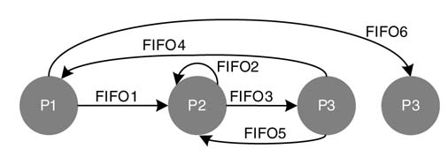
Exercise 4.12
Check whether the DFG given in Figure 4.46 is consistent. If it is not, what minimum changes in the production or consumption rates can convert it into a consistent DFG. Give a self-timed firing sequence of a consistent DFG.
Figure 4.46 DFG consisting of two nodes (exercise 4.12)
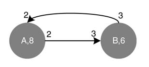
Exercise 4.13
Convert the SDFG shown in Figure 4.47 into HSDFG. Compute the throughput of the graph and also give a hardware realization of the DFG.
Figure 4.47 SDFG consisting of three nodes (exercise 4.13)
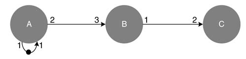
Exercise 4.14
Convert the SDFG given in Figure 4.48 into HSDFG. Give a synthesis realization of the DFG.
Figure 4.48 SDFG consisting of two nodes (exercise 4.14)
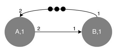
Exercise 4.15
The DFG given in Figure 4.49 implements an M-JPEG algorithm. Draw a KPN showing FIFOs.
Figure 4.49 DFG implementing M-JPEG compression algorithm (exercise 4.15)
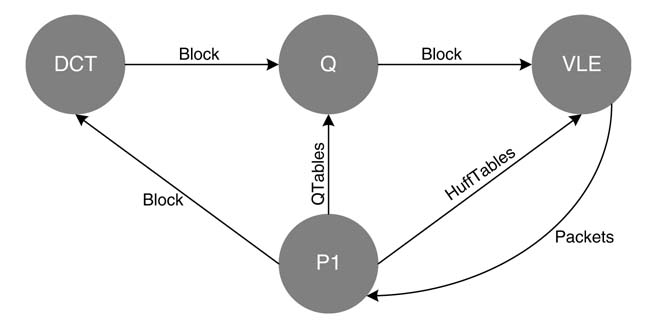
Figure 4.50 Cyclo-static DFG for 3/2 sampling rate change (exercise 4.16)
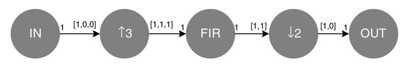
Exercise 4.16
A digital up/down converter can be realized as a cyclo-static DFG. The production and consumption rate as vectors in the DFG given in Figure 4.50 implement a 3/2 digital up/down converter. Design the registers and multiplexer to realize the design in HW.
Exercise 4.17
Draw a multi-dimensional DFG implementing a level-3 discrete wavelet transform based on sub-band decomposition of a 256 × 256 gray image. State the consumption and production rates on each edge. Also specify the buffer size requirements on the edges.
Exercise 4.18
For the HSDF given in Figure 4.51, compute the following:
1.a self-timed schedule for the graph;
2.a repetition vector based on the solution of balanced equations;
3.a hardware synthesis of the graph.
Exercise 4.19
For the SDFG given in Figure 4.52:
1.Write its topology matrix.
2.By computing the rank of the matrix computed in (1), determine whether the graph represents a consistent or an inconsistent SDFG.
Figure 4.51 Graph implementing an HSDFG (exercise 4.18)
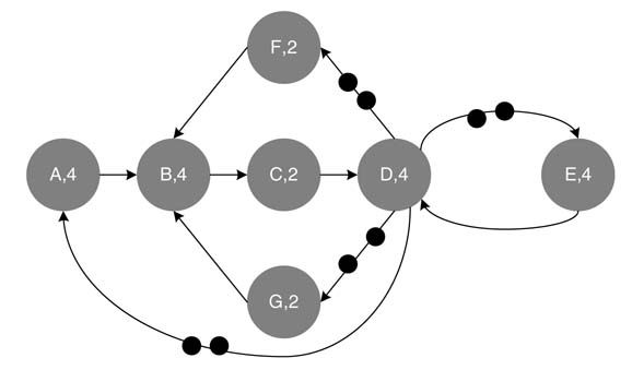
Figure 4.52 SDFG with three nodes (exercise 4.19)
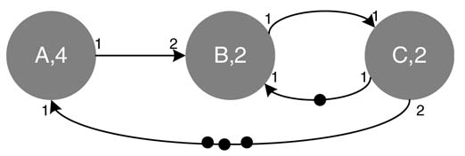
3.Compute the repetition vector of the graph.
4.Map the DFG to hardware, assuming node A gets one sample of the input data at every sample clock. Clearly draw registers realizing delays and registers at cross-node boundaries clocked with the circuit clock.
5.Convert the graph to an HSDFG.
Exercise 4.20
The flow graph of Figure 4.53 shows a multi-rate DFG.
1.Design a sequential HW realization of the graph showing all the multiplexers, demultiplexers, registers and clocks in the design.
2.Write RTL Verilog code to implement the design in hardware.
3.Write balanced equations for the graph and solve the equations to find a parallel HW realization of the design. Draw the realization.
Figure 4.53 A multi-rate DFG (exercise 4.20)
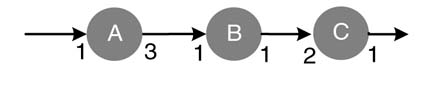
References
1.R. G. Vaughan, N. L. Scott and D. R. White, “The theory of bandpass sampling,” IEEE Transactions on Signal Processing, 1991, vol. 39, pp. 1973-1984.
2.C.-H. Tseng and S.-C. Chou, “Direct down-conversion of multiband RF signals using bandpass sampling,” IEEE Transactions on Wireless Communications, 2006, vol. 5, pp. 72-76.
3.G. Kahn, “The semantics of a simple language for parallel programming,” Information Processing, 1974, pp. 471–475.
4.E. A. Lee and T M. Parks, “Dataflow process networks,” in Proceeding of the IEEE, 1995, vol. 83, pp. 773-799.
5.E. Cheung, H. Hsieh and F. Balarin, “Automatic buffer sizing for rate-constrained KPN applications on multiprocessor system-on-chip,” in Proceedings of IEEE International High-level Design Validation and Test Workshop, 2007, pp. 37-44.
6.T Stefanov, C. Zissulescu, A. Turjan, B. Kienhuis and E. Deprettere, “System designusing Kahn process networks: the Compaan/Laura approach,” in Proceedings of Design, Automation and Testing in Europe Conference, Paris, 2004, pp. 340-345, IEEE Computer Society, Washington, USA.
7.S. Derrien, A. Turjan, C. Zissulescu, B. Kienhuis and E. Deprettere, “Deriving efficient control in process networks with Compaan/Laura,” International Journal of Embedded Systems, 2008, vol. 3,no. 3, pp. 170-180.
8.K. Huang, D. Grunert and L. Thiele, “Windowed FIFOs for FPGA-based multiprocessor systems,” in Proceedings of 18th IEEE International Conference on Application-specific Systems, pp. 36-41, Zurich, 2007.
9.A.V. Oppenheim, R. W. Schafer and J. R. Buck, Discrete-time Signal Processing, 2nd edn, 1999, Prentice-Hall.
10.H. Nikolov, T Stefanov and E. Deprettere, “Systematic and automated multiprocessor system design, programming and implementation,” IEEE Transactions on Computer-Aided Design of Integrated Circuits and Systems, 2008, vol. 27, pp. 542-555.
11.R. Ohlendorf, M. Meitinger, T Wild and A. Herkersdorf, “A processing path dispatcher in network processor MPSoCs,” IEEE Transactions on Very Large Scale Integration Systems, 2008, vol. 16, pp. 1335-1345.
12.Leiden University. Compaan: www.liacs.nl/~cserc/compaan
13.www.mathworks.com/products/simulink
14.http://eesof.tm.agilent.com/products/ads_main.xhtml
17.National Instruments. NI LabVIEW: www.ni.com/labview/
18.Seoul National University. PeaCE (codesign environment): //peace.snu.ac.kr/research/peace/
19.StreamIt: groups.csail.mit.edu/cag/streamit/
20.M. G. Corporation. Mentor Graphics: www.mentor.com
21.SIGNALogic. Hypersignal: www.signalogic.com
22.University of Berkeley. Ptolemy: //ptolemy.berkeley.edu
23.University of New Mexico. Khoros: www.unm.edu
24.E. A. Lee and D. G. Messerschmitt, “Static scheduling of synchronous data-flow programs for digital signal processing,” IEEE Transactions on Computing, 1987, vol. 36, pp. 24-35.
25.C.-J. Hsu,“Dataflow integration and simulation techniques for DSP system design tools,” PhD thesis, University of Maryland, College Park, USA, 2007.
26.W. Khan and V. Dimitrov, “Multiplierless DCT algorithm for image compression applications,” International Journal of Information Theories and Applications, 2004, vol. 11, no. 2, pp. 162-169.
27.M. T Sun, T C. Chen and A. M. Gottlieb, “VLSI implementation of a 16 × 16 discrete cosine transform,” IEEE Transactions on Circuits and Systems, 1989, vol. 36, pp. 610-617.
28.L. V Agostini, I. S. Silva and S. Bampi, “Pipelined fast 2-D DCT architecture for JPEG image compression,” in Proceedings of 14th Symposium on Integrated Circuits and Systems Design, 2001, pp. 226-231, IEEE Computer Society, USA.
29.K. Kim, H. J. Cho and J. J. Cha, “A design of 2-D DCT/IDCT for real-time video applications,” in Proceedings of 6th International Conference on VLSI and CAD, 1999, pp. 557-559, Seoul, South Korea.
30.L. Benini, P. Siegel and G. De Micheli, “Automatic synthesis of gated clocks for power reduction in sequential circuits,” IEEE Design and Test of Computers, 1994, vol. 11, pp. 32–40.
31.L. Benini and G. De Micheli, “Transformation and synthesis of FSMs for low-power gated clock implementation,” IEEE Transactions on Computer-Aided Design of Integrated Circuits and Systems, 1996, vol. 15, pp. 630–643.
32.L. Benini,G. De Micheli, E. Macii, M. Poncino and R. Scarsi, “Symbolic synthesis of clock-gating logic for power optimization of control-oriented synchronous networks,” in Proceedings of European Design and Test Conference, Paris, 1997, pp. 514–520, IEEE Computer Society, Washington, USA.
33.H. Jung, H. Yang and S. Ha, “Optimized RTL code generation from coarse-grain dataflow specification for fast HW/SW cosynthesis,” Journal of VLSI Signal Processing, June 2007 [online].
34. H. Jung, K. Lee and S. Ha, “Efficient hardware controller synthesis for synchronous data flow in system level design,” IEEE Transactions on Very Large Scale Integration Systems, 2002, vol. 10, pp. 423–428.