
1
Overview
No exponential is forever ... but we can delay “forever”
1.1 Introduction
This chapter begins from the assertion that the advent of VLSI (very large scale integration) has enabled solutions to intractable engineering problems. Gordon Moore predicted in 1965 the rate of development of VLSI technology, and the industry has indeed been developing newer technologies riding on his predicted curve. This rapid advancement has led to new dimensions in the core subject of VLSI. The capability to place billions of transistors in a small silicon area has tested the creativity of engineers and scientists around the world. The subject of digital design for signal processing systems embraces these new challenges. VLSI has revolutionized the commercial market, with products regularly appearing with increasing computational power, improved battery life and reduced physical size.
This chapter discusses several applications. The focus of the book is on applications primarily in areas of signal processing, multimedia, digital communication, computer networks and data security. Some of the applications are shown in Figure 1.1.
Multimedia applications have had a dramatic impact on our lives. Multimedia access on hand held devices such as mobile phones and digital cameras is a direct consequence of this technology.
Another area of application is high-data-rate communication systems. These systems have enormous real-time computational requirements. A modern mobile phone, for example, executes several complex algorithms, including speech compression and decompression, forward error-correction encoding and decoding, highly complex modulation and demodulation schemes, up-conversion and down-conversion of modulated and received signals, and so on. If these are implemented in software, the amount of real-time computation may require the power of a supercomputer. Advancement in VLSI technology has made it possible to conveniently accomplish the required computations in a hand-held device. We are also witnessing the dawn of new trends like wearable computing, owing much to this technology.
Figure 1.1 VLSI technology plays a critical role in realizing real-time signal processing systems
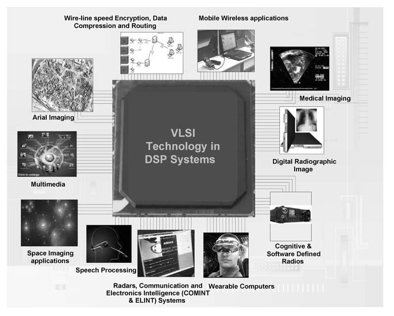
Broadband wireless access technology, processing many megabits of information per second, is another impressive display of the technology, enabling mobility to almost all the services currently running on desktop computers. The technology is also at work in spacecraft and satellites in space imaging applications.
The technology is finding uses in biomedical equipment, examples being digital production of radiographic and ultrasound images, and implantable devices such as the cardioverter defibrillator that acquires and digitizes heartbeats, detects any rhythmic abnormalities and symptoms of sudden cardiac arrest and applies an electric shock to help a failing heart.
This chapter selects a mobile communication system as an example to explain the design partitioning issues. It highlights that digital design is effective for mapping structured algorithms in silicon. The chapter also considers the design of a backplane of a high-end router to reveal the versatility of the techniques covered in this book to solve problems in related areas where performance is of prime importance.
The design process has to explore competing design objectives: speed, area, power, timing and so on. There are several mathematical transformations to help with this. Keeping in perspective the defined requirement specifications, transformations are applied that trade off less relevant design objectives against the other more important objectives. That said, for complex design problems these mathematical transformations are of less help, so an effective approach requires learning several ‘tricks of the trade’. This book aims to introduce the transformations as well as giving tips for effective design.
The chapter highlights the impact of the initial ideas on the entire design process. It explains that the effect of design decisions diminishes as the design proceeds from concept to implementation. It establishes the rational for the system architect to positively impact the design process in the right direction by selecting the best option in the multidimensional design space. The chapter explores the spectrum of design options and technologies available to the designer. The design options range from the most flexible general-purpose computing machine like Pentium, to commercially available off-the-shelf digital signal processors (DSPs), to more application-specific instruction-set processors, to hard-wired application-specific designs yielding best performance without any consideration of flexibility in the solution. The chapter describes the target technologies on which the solution can be mapped, like general-purpose processors (GPPs), DSPs, application-specific integrated circuits (ASICs), and field-programmable gate arrays (FPGAs). It is established that, for complex applications, an optimal solution usually consists of a mix of these target technologies.
This chapter presents some design examples. The rationale for design decisions for a satellite burst modem receiver is described. There is a brief overview of the design of the backplane of a router. There is an explanation of the design of a network-on-chip (NoC) carrier-class VoIP media gateway. These examples follow a description of the trend from digital-only design to mixed-signal system-on-chips (SoCs). The chapter considers synchronous digital circuits where digital clocks are employed to make all components operate synchronously in implementing the design.
1.2 Fueling the Innovation: Moore’s Law
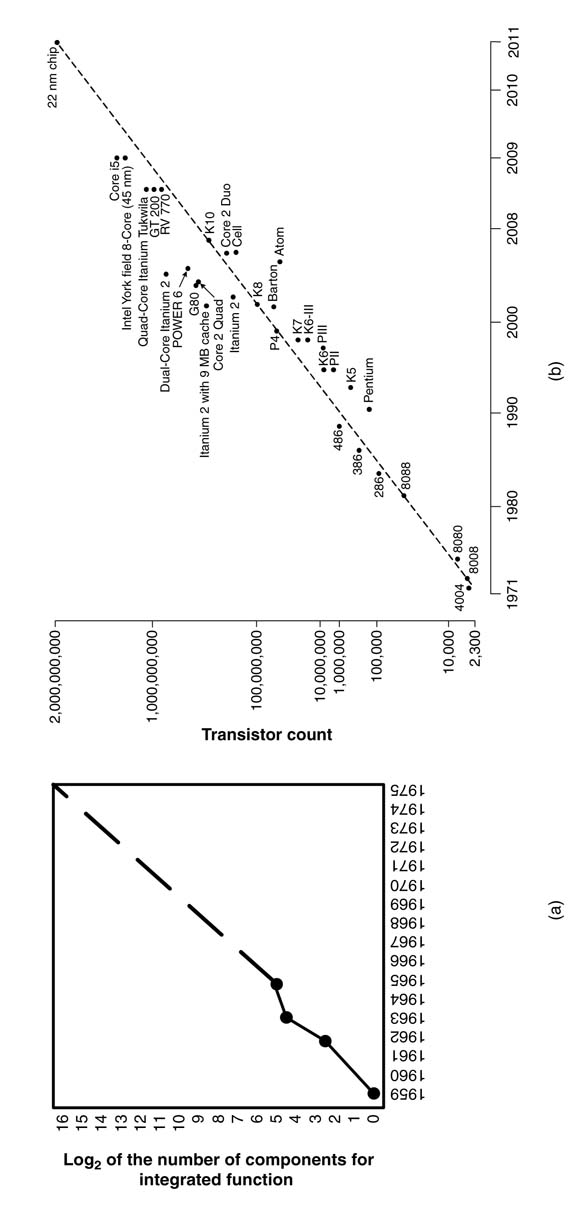
Advancements in VLSI over a few decades have played a critical role in realizing the amazing electronic gadgets we live with today. Gordon Moore, founder of Intel, earlier predicted the rapid rate of these advancements. In 1965 he noted that the number of transistors on a chip was doubling every 18 to 24 months. Figure 1.2(a) shows the predicted curve known as Moore’s Law from his original paper [1]. This ‘law’ has fueled innovation for five decades. Figure 1.2(b) shows Intel’s response to his prediction.
Moore acknowledges that the trend cannot last forever, and he gave a presentation at an international conference, entitled “No exponential is forever, but we can delay ‘forever’” [2]. Intel has plans to continue riding on the Moore’s Law curve for another ten years and has announced a 2.9 billion-transistor chip for the second quarter of 2011. The chip will fit into an area the size of a fingernail and use 22-nanometer technology [3]. For comparison, the Intel 4004 microprocessor introduced in 1971 was based on a 10 000-nanometer process.
Integration at this scale promises enormous scope for designers and developers, and the development of design tools has matched the pace. These tools provide a level of abstraction so that the designer can focus more on higher level design concepts rather than low-level details.
1.3 Digital Systems
1.3.1 Principles
To examine the scope of the subject of digital design, let us consider an embedded signal processing system of medium complexity. Usually such a system consists of heterogeneous physical devices such as a GPP or micro-controller, multiple DSPs, a few ASICs, and FPGAs. An application implemented on such a system usually consists of numerous tasks of varying computational complexity. These tasks are mapped on to the physical devices. The decision to implement a particular task on a particular device is based on the computational complexity of the task, its code density, and the communication it requires with other tasks.
Figure 1.2 (a) The original prediction of Moore’s Law. (b) Intel’s response to Moore’s prediction
The computationally intensive (‘number-crunching’) tasks of the application can be further divided into categories. The tasks for which commercial off-the-shelf ASICs are available are best mapped on these devices. ASICs are designed to perform specific functions of a particular application and are not programmable, as are GPPs. Based on the target technology, ASICs are of different types, examples of which are full-custom, standard-cell-based, gate-array-based, channeled gate array, channel-less gate array, and structured gate array. As these devices are application-specific they are optimized using integrated-circuit manufacturing process technology. These devices offer low cost and low power consumption. There are many benefits to using ASICs, but because of their fixed implementation a design cannot be made easily up gradable.
It is important to point out that several applications implement computationally intensive but non-standard algorithms. The designer, for these applications, may find that mapping the entire application on FPGAs is the only option for effective implementation. For applications that consist of standard as well as non-standard algorithms, the computationally intensive tasks are further divided into two groups: structured and non-structured . The tasks in the structured group usually consist of code that has loops or nested loops with a few instructions being repeated a number of times, whereas the tasks in the non-structured group implement more code-intensive components. The structured tasks are effectively mapped on FPGAs, while the non-structured parts of the algorithm are implemented on a DSP or multiple DSPs.
A field-programmable gate array comprises a matrix of configurable logic blocks (CLBs) embedded in an interconnected net. The FPGA synthesis tools provide a method of programming the configurable logic and the interconnects. The FPGAs are bought off the shelf: Xilinx [4], Altera [5], Atmel [6], Lattice Semiconductor [7], Actel [8] and Quick Logic [9] are some of the prominent vendors. Xilinx shares more than 50% of the programmable logic device (PLD) segment of the semiconductor industry.
FPGAs offer design reuse, and better performance than a software solution mapped on a DSP or GPP. They are, however, more expensive and give reduced performance and more power consumption compared with an equivalent ASIC solution if it exists. The DSP, on the other hand, is a microprocessor whose architecture is specially designed to support number-crunching signal processing applications. Usually a DSP can perform many multiplication and addition operations and supports special addressing modes that help in effective implementation of fast Fourier transform (FFT) and convolution algorithms.
The GPPs or microcontrollers are general-purpose computing machines. Types are ‘complex instruction set computer’ (CISC) and ‘reduced instruction set computer’ (RISC).
The tasks specific to user interfaces, control processes and other code-intensive protocols are usually mapped on GPPs or microcontrollers. For handling multiple concurrent tasks, events and interrupts, the microcontroller runs a real-time operating system. The GPP is also good at performing general tasks like configuring various devices in the system and interfacing with external devices. The microcontroller or GPP performs the job of a system controller. For systems of medium complexity, it is connected to a shared bus. The processor configures the ASICs and FGPAs, and also bootstraps the DSPs in the system. A high-speed bus like Amba High-speed Bus (AHB) is used in these systems [10]. The shared-bus protocol allows only one master to transfer the data. For designs that require parallel transfer of data, a multi-layer shared bus like Multilayer AHB (ML-AHB) is used [11]. The microcontroller also interfaces with the external displays and control panels.
Figure 1.3 An embedded signal processing system with DSPs, FPGAs, ASICs and GPP
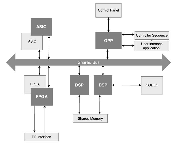
The digital design of a digital communication system interfaces with the RF front end. For voice-based applications the system also contains CODEC (more in Chapter 12) with associated analog interfaces. The FPAGs in the system also provide glue logic and interfaces with other devices in the system. There may also be dual-port RAM to provide shared memory to multiple DSPs in the system. A representative system is shown in Figure 1.3.
1.3.2 Multi-core Systems
Many applications are best mapped on general-purpose processors. As high-end computing applications demand more and more computational power in programmable devices, the vendors of GPPs are in corporating multiple cores of GPPs in a single SoC configuration. Almost all the vendors of GPPs, such as Intel, IBM, Sun Microsystems and AMD, are now placing multiple cores on a single chip for improved performance and high reliability. Examples are Intel’s York field 8-core chip in 45-nm technology, Intel’s 80-core teraflop processor, Sun’s Rock 8-core CPU, Sun’s UltraSPARCT1 8-core CPU, and IBM’s 8-core POWER7. These multi-core solutions also offer the necessary abstraction, whereby the programmer need not be concerned with the underlying complex architecture, and software development tools have been produced that partition and map applications on these multiple cores. This trend is continuously adding complexity to digital design and software tool development. From the digital design perspective, multi processors based systems are required to communicate with each other, and inter-processors connections need to be scalable and expendable. The network-on-chip (NoC) design paradigm addresses issues of scalability of on-chip connectivity and inter-processor communication.
1.3.3 NoC-based MPSoC
Besides GPP-based multi-core SoCs for mapping general computing applications, there also exist other application-specific SoC solutions. An SoC integrates all components of a system in a single chipset. That includes microprocessor, application-specific accelerators, all interfaces to memory and peripheral devices, and so on.
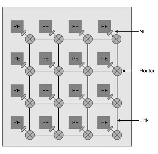
Most high-end signal processing applications offer an inherent parallelism. To exploit this parallelism, these systems are mapped on multiple heterogeneous processors. Traditionally these processors are connected with shared memories on shared buses. As complex designs are integrating an increasing number of multi-processors on a single SoC (MPSoC) [12], designs based on a shared bus are not effective owing to complex arbitration, clock skews and latency issues. These designs require scalable and effective communication infrastructure. An NoC offers a good solution to these problems [13]. The NOC provides higher bandwidth, low latency, modularity, scalability, and a high level of abstraction to the system. The complex bus protocols route wires to connect various components, whereas an NOC uses packet-based protocols to provide connectivity among components. The NoC enables parallel transactions of data.
The basic architecture of an NOC is shown in Figure 1.4. Each processing element (PE) is connected to an on-chip router via a network interface (NI) controller.
Figure 1.4 An NoC-based heterogeneous multi-core SoC design
Many vendors are now using NoC to integrate multiple PEs on a single chip. A good example is the use of NoC technology in the Play Station 3 (PS3) system by Sony Entertainment. A detailed design of an NoC-based system is given in Chapter 13.
1.4 Examples of Digital Systems
1.4.1 Digital Receiver for a Voice Communication System
A typical digital communication system for voice, such as a GSM mobile phone, executes a combination of algorithms of various types. A system-level block representation of these algorithms is shown in Figure 1.5. These algorithms fall into the following categories.
1.Code-intensive algorithms . These do not have repeated code. This category consists of code for phone book management, keyboard interface, GSM (Global System for Mobile) protocol stack, and the code for configuring different devices in the system.
2.Structured and computationally intensive algorithms . These mostly take loops in software and are excellent candidates for hardware mapping. These algorithms consist of digital up- and down-conversion, demodulation and synchronization loops, and forward error correction (FEC).
3.Code-intensive and computationally intensive algorithms . These lack any regular structure. Although their implementations do have loops, they are code-intensive. Speech compression is an example.
The GSM is an interesting example of a modern electronic device as most of these devices implement applications that comprise these three types of algorithm. Some examples are DVD players, digital cameras and medical diagnostic systems.
The mapping decisions on target technologies are taken at a system level. The code-intensive part is mapped on a microcontroller; the structured parts of computationally intensive components of the application, if consisting of standard algorithms, are mapped on ASICs or otherwise they are implemented on FPGAs; and the computational and code-intensive parts are mapped on DSPs.
Figure 1.5 Algorithms in a GSM transmitter and receiver and their mapping on to conventional target technologies consisting of ASIC, FPGA and DSP
It is also important to note that only signals that can be acquired using an analog-to-digital (A/D) converter are implemented in digital hardware (HW) or software (SW), whereas the signal that does not meet the Nyquist sampling criterion can be processed only using analog circuitry. This sampling criterion requires the sampling rate of an A/D converter to be double the maximum frequency or bandwidth of the signal. A consumer electronic device like a mobile phone can only afford to have an A/D converter in the range 20 to 140 million samples per second (Msps). This constraint requires analog circuitry to process the RF signal at 900 MHz and bring it down to the 10–70 MHz range. After conversion of this to a digital signal by an A/D converter, it can be easily processed. A conventional mapping of different building blocks of a voice communication system is shown in Figure 1.5.
It is pertinent to mention that, if the volume production of the designed system are quite high, a mixed-signal SoC is the option of choice. In a mixed-signal SoC, the analog and digital components are all mapped on a single silicon device. Then, instead of placing physical components, the designer acquires soft coresor hard cores of the constituent components and integrates them on a single chip.
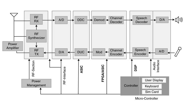
An SoC solution for the voice communication system is shown in Figure 1.6. The RF microcontroller, DSP and ASIC logic with on-chip RAM and requisite interfaces are all integrated on the same chip. A system controller controls all the interfaces and provides glue logic for all the components to communicate with each other on the device.
Figure 1.6 A system-on-chip solution
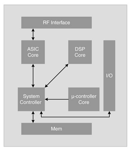
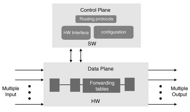
Figure 1.7 HW-SW partitioning of control and data plane in a router
1.4.2 The Backplane of a Router
A router consists mainly of two parts or planes, a control/management plane and a data plane. A code-intensive control or management plane implements the routing algorithms. These algorithms are executed only periodically, so they are not time-critical.
In contrast, the data plane of the router implements forwarding . A routing algorithm updates the routing table, after which a forwarding logic uses this table to transfer data from input ports to output ports. This forwarding logic is very critical as it executes all the time, and is implemented as the data plane. This plane checks the packet header of the inbound packets and, from a lookup table, finds its destination port. This operation is performed on all the data packets received by the router and is very well structured and computationally intensive. For routers supporting gigabit or multi-gigabit rates, this part is usually implemented in hardware [14], whereas the routing algorithms are mapped in software as they are code-intensive.
These planes and their effective mappings are shown in Figure 1.7.
1.5 Components of the Digital Design Process
A thorough understanding of the main components of the digital design process is important. The subsequent chapters of this book elaborate on these components, so they are discussed only briefly here.
1.5.1 Design
The ‘design’ is the most critical component of the digital design process. The top-level design highlights the partitioning of the system into its various components. Each component is further defined at the register transfer level (RTL). This is a level of abstraction where the digital designer specifies all the registers and elaborates how data will flow through these registers. The combinational logic between two sets of registers is usually described using high-level mathematical operations, and is drawn as a cloud.
1.5.2 Implementation
When the design has been described at RTL level, its implementation is usually a straightforward translation in a hardware description language (HDL) program. The program is then synthesized for mapping on an FPGA or ASIC implementation.
1.5.3 Verification
As the number of gates on a single silicon device increases, so do the challenges of verification. Verification is also critical in VLSI design as there is hardly any tolerance for bugs in the hardware. With application-specific integrated circuits, a bug may require a re-spin of fabrication, which is expensive, so it is important for an ASIC to be ‘right first time’. Even bugs found in FPGA-based designs result in extended design cycles.
1.6 Competing Objectives in Digital Design
To achieve an effective design, a designer needs to explore the design space for tradeoffs of competing design objectives. The following are some of the most critical design objectives the designer needs to consider:
- area
- critical path delays
- testability
- power dissipation.
The art of digital design is to find the optimal tradeoff among these. These objectives are competing because, for example, if the designer tries to minimize area then the design may result in longer critical paths and may also affect the testability of the design. Similarly, if the design as synthesized for better timing means shorter critical paths, the design may result in a larger area. Better timing also means more power dissipation, which depends directly on the clock frequency. It is these competing objectives that make learning the techniques covered in this book very pertinent for designers.
1.7 Synchronous Digital Hardware Systems
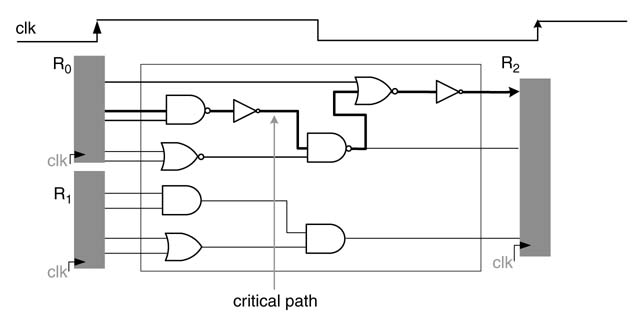
The subject of digital design has many aspects. For example, the circuit may be synchronous or asynchronous , and it may be analog or digital . A digital synchronous circuit is always an option of choice for the designer. In synchronous digital hardware, all changes in the system are controlled by one or multiple clocks. In digital systems, all inputs/outputs and internal values can take only discrete values.
Figure 1.8 depicts an all-digital synchronous circuit in which all changes in the system are controlled by a global clock clk. A synchronous circuit has a number of registers, and values in these registers are updated at the occurrence of positive or negative edges of the clock signal. The figure shows positive-edge triggered registers. The output signal from the registers R0 and R1 are fed to the combinational logic. The signal goes through the combinational logic which consists of gates. Each gate causes some delay to the input signal. The accumulated delay on each path must be smaller than the time period of the clock, because the signal at the input of R2 register must be stable before the arrival of the next active edge of the clock. As there are a number of paths in any digital design, the longest path – the path that takes the maximum time for the signal to settle at the output – is called the critical path , as noted in Figure 1.8. The critical path of the design should be smaller than the permissible delay determined by the clock cycle.
Figure 1.8 Example of a digital synchronous hardware system
1.8 Design Strategies
At the system level, the designer has a spectrum of design options as shown in Figure 1.9. It is very critical for the system designer to make good design choices at the conceptual level because they will have a deep impact on the rest of the design cycle. At the system design stage the designer needs only to draw a few boxes and take major design decisions like algorithm partitioning and target technology selection.
Figure 1.9 Target technologies plotted against flexibility and power consumption
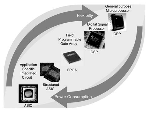
If flexibility in programming is required, and the computational complexity of the application is low, and cost is not a serious consideration, then a general-purpose processor such as Intel’s Pentium is a good option. In contrast, while implementing computationally intensive non-structured algorithms, flexibility in terms of programming is usually a serious consideration, and then a DSP should be the technology of choice.
In many applications the algorithms are computationally intensive but are also structured. This is usually the case in image and video processing applications, or a high-data-rate digital communication receiver. In these types of application the algorithms can be mapped on FPGAs or ASICs. While implementing algorithms on FPGAs there are usually two choices. One option is to design an application-specific instruction-set processor (ASIP). This type of processor is programmable but has little flexibility and can port only the class of applications using its application-specific instruction set. In the extreme case where performance is the only consideration and flexibility is not required, the designer should choose a second option, whereby the design is dedicated to that particular application and logic is hardwired without giving any consideration to flexibility. This book discusses these two design options in detail.
The performance versus flexibility tradeoff is shown in Figure 1.10. It is interesting to note that, in many high-end systems, usually all the design options are exercised. The code-intensive part of the application is mapped on GPPs, non-structured signal processing algorithms are mapped on DSPs, and structured algorithms are mapped on FPGAs, whereas for standard algorithms ASICs are used. This point is further elaborated in the design examples later.
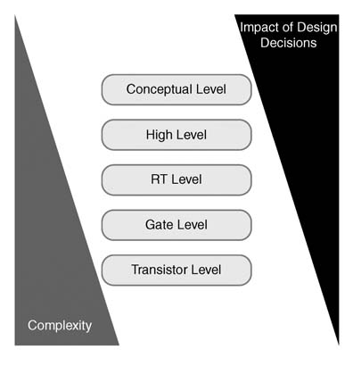
These apparently simple decisions are very critical once the system proceeds along the design cycle. The decisions are especially significant for the blocks that are partitioned for hardware mapping. The algorithms are analyzed and architectures are designed. The designer either selects ASIP or dedicated hard-wired. The designer takes the high-level design and starts implementing the hardware. The digital design is implemented at RTL level and then it is synthesized and tools translate the code to gate level. The synthesized design is physically placed and routed. As the design goes along the design cycle, the details are very complex to comprehend and change. The designer at every stage has to make decisions, but as the design moves further along the cycle these decisions have less impact on the overall function and performance of the design. The relationship between the impact of the design decision and its associated complexity is shown in Figure 1.11.
Figure 1.10 Efficiency verses flexibility tradeoff while selecting a design option
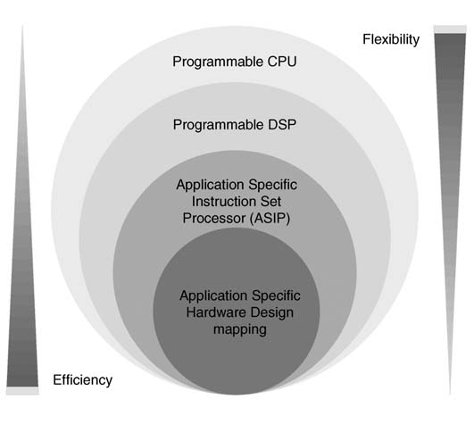
Figure 1.11 Design decision impact and complexity relationship diagram
1.8.1 Example of Design Partitioning
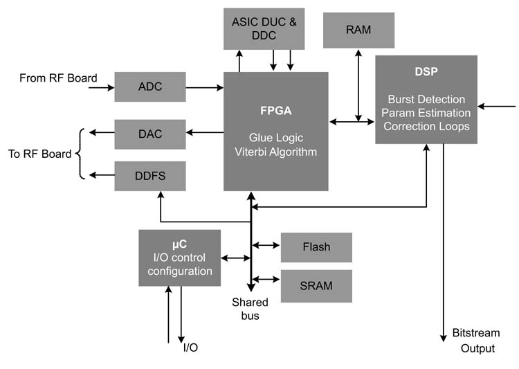
Let us consider an example that elaborates on the rationale of mapping a communication system on a hybrid platform. The system implements an upto 512Kbps BPSK/QPSK (phase-shift keying) satellite burst modem.
The design process starts with the development of an algorithm in MATLAB®. The code is then profiled. The algorithm consists of various components. The computation and storage requirements of each component along with inter-component communication are analyzed. The following is a list of operations that the digital receiver performs.
- Analog to digital conversion (ADC) of an IF signal at 70 MHz at the receiver (Rx) using band-pass sampling.
- Digital to analog conversion (DAC) of an IF signal at 24.5 MHz at the transmitter (Tx).
- Digital down-conversion of the band-pass digitized IF signal to baseband at the Rx. The baseband signal consists of four samples per symbol on each I and Q channel. For 512 Kbps this makes 2014 Ksps (kilo samples per second) on both the channels.
- Digital up-conversion of the baseband signal from 2014 ksps at both I and Q to 80 Msps at the Tx.
- Digital demodulator processing 1024 K complex samples per second. The algorithm at the Rx consists of: start of burst detection, header removal, frequency and timing loops and slicer.
In a burst modem, the receiver starts in burst detection state. In this state the system executes the start of the burst detection algorithm. A buffer of data is input to the function that computes some measure of presence of the burst. If the measure is greater than a threshold, ‘start of burst’ (SoB) is declared. In this state the system also detects the unique word (UW) in the transmitted burst and identifies the start of data. If the UW in the received burst is not detected, the algorithm transits back into the burst detection mode. When both the burst and the UW are detected, then the algorithm transits to the estimation state. In this state the algorithm estimates amplitude, timing, frequency and phase errors using the known header placed in the transmitted burst. The algorithm then transits to the demodulation state. In this state the system executes all the timing, phase and frequency error-correction loops. The output of the corrected signal is passed to the slicer. The slicer makes the soft and hard decisions. For forward error correction (FEC), the system implements a Viterbi algorithm to correct the bit errors in the slicer soft decision output, and generates the final bits [15]. The frame and end off rame are identified. In a burst, the transmitter can transmit several frames. To identify the end of the burst, the transmitter appends a particular sequence in the end of the last frame. If this sequence is detected, the receiver transits back to the SoB state. The state diagram of the sequence of operation in a satellite burst modem receiver is shown in Figure 1.12.
The algorithm is partitioned to be mapped on different components based on the nature of computations required in implementing the sub-components in the algorithm. The following mapping effectively implements the system.
- A DSP is used for mapping computationally intensive and non-regular algorithms in the receiver. These algorithms primarily consist of the demodulator and carrier and timing recovery loops.
- ASICs are used for ADC, DAC, digital down-conversion (DDC) and digital up-conversion (DUC).A direct digital frequency synthesis (DDFS) chip is used for cosine generation that mixes with the baseband signal.
- An FPGA implements the glue logic and maps the Viterbi algorithm for FEC. The algorithm is very regular and is effectively mapped in hardware.
A micro controller is used to interface with the control panel and to configure different components in the system. A block diagram of the system highlighting the target technologies and their interconnection is shown in Figure 1.13.
Figure 1.12 Sequence of operations in a satellite burst modem receiver
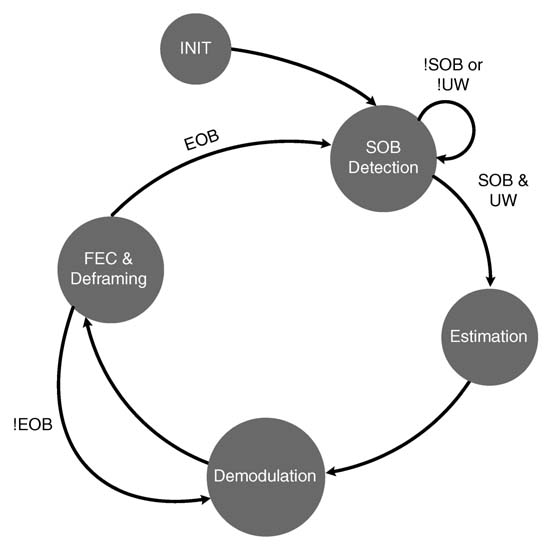
Figure 1.13 System-level design of a satellite burst receiver
1.8.2 NoC-based SoC for Carrier-class VoIP Media Gateway
VoIP systems connect the legacy voice network with the packet network such that voice, data and associated signaling information are transported on the IP network. In the call setup stage, the signaling protocol (e.g. session initiation protocol, SIP) negotiates parameters for the media session. After the call is successfully initiated, the media session is established. This session takes the uncompressed digitized voice from the PSTN (public switched telephone network) interface and compresses and packages it before it is transported on a packet network. Similarly it takes the incoming packeted data from the IP network and decompresses it before it is sent on the PSTN network. A carrier-class VoIP media gateway processes hundreds of these channels.
The design of an SoC for a carrier-class VoIP media gateway is given in Figure 1.14. A matrix of application-specific processing elements are embedded in an NOC configuration on an SoC. In carrier-class application the SoC processes many channels of VoIP [16]. Each channel of VoIP requires the system to implement a series of algorithms. Once a VoIP call is in progress, the SoC needs to first process ‘line echo cancellation’ (LEC) and ‘dual-tone multi-frequency’ (DTMF) detection on each channel, and then it decompresses the packeted voice and compresses the time-division multiplex (TDM) voice. The SoC has two interfaces, one with the PSTN network and the other with the IP network. The interface with the PSTN may be an H.110 TDM interface. Similarly the interfaces on the IP side may be a combination of POS, UTOPIA or Ethernet. Besides these interfaces, the SoC may also have interfaces for external memory and PCI Express (PCIe). All these components on a chip are connected to a NOC for inter-component communication.
Figure 1.14 NoC-based SoC for carrier-class VoIP applications. Multiple layers of application-specific PEs are attached with an NoC for inter-processor communication
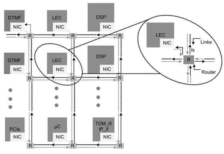
The design assumes that the media gateway controller and packet processor are attached with the media gateway SoC for complete functionality of a VoIP system. The packets received on the IP interface are saved in external memory. The data received on the H.110 interface is buffered in an on-chip memory before being transferred to the external memory. An on-chip RISC microcontroller is intimated to process an initiated call on a specified TDM slot by the host processor on a PCIe interface.
The microcontroller keeps a record of all the live calls, with associated information like the specification on agreed encoder and decoder between caller and callee. The microcontroller then schedules these calls on the array of multiprocessors by periodically assigning all the tasks associated with processing a channel that includes LEC, in-voice DTMF detection, encoding of TDM voice, and decoding of packeted voice. The PEs program external DMA for fetching TDM voice data for compression and packeted voice for decompression. The processor also needs to bring the context from external memory before it starts processing a particular channel. The context has the states of different variables and arrays saved while processing the last frame of data on a particular channel.
The echo is produced at the interface of 4-line to 2-line hybrid at the CO office. Owing to impedance mismatch in the hybrid, the echo of far-end speech is mixed in the near-end voice. This echo needs to be cancelled before the near-end speech is compressed and packetized for transmission on an IP network. An LEC processing element is designed to implement line echo cancellation. The LEC processing also detects double talk and updates the coefficients of the adaptive filter only when line echo is present in the signal and the near end is silent. There is an extended discussion of LEC and its implementation in Chapter 11.
Each processing element in the SoC is scheduled to perform a series of tasks for each channel. These tasks for a particular channel are periodically assigned to a set of PEs. Each PE keeps checking the task list, while it is performing the currently assigned task. Finding a new task in the task list, the PE programs a channel of the DMA to bring data and context for this task into on-chip memory of the processor. Similarly, if the processor finds that it is tasked to perform an algorithm where it also needs to bring the program into its program memory (PM), the PE also requests the DMA to fetch the code for the next task in the PM of the PE. This code fetching is kept to a minimum by carefully scheduling the tasks on the PEs that already have programs of the assigned task in its PM.
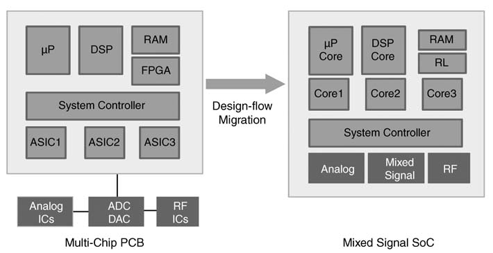
1.8.3 Design Flow Migration
As explained earlier, usually the communication system requires component-level integration of different devices to implement digital baseband, RF transmitter and receiver, RF oscillator and power management functionality. The advancement in VLSI technology is now enabling the designer to integrate all these technologies on the same chip.
Although the scope of this book is limited to studying digital systems, it is very pertinent to point out that, owing to cost, performance and power dissipation considerations, the entire system including the analog part is now being integrated on a single chip. This design flow migration is show in Figure 1.15. The ASICs and microcontroller are incorporated as intellectual property (IP) cores and reconfigurable logic (RL) of the FPGAs is also placed on the same chip. Along with digital components, RF and analog components are also integrated on the same chip. For example, a mixed-signal integrated circuit for a mobile communication system usually supports ADC and DAC for on-chip analog-to-digital and digital-to-analog conversion of baseband signals, phase-locked loops (PLLs) for generating clocks for various blocks, and codec components supporting PCM and other standard formats [17]. There are even integrated circuits that in corporate RF and power management blocks on the same chip using deep sub-micron CMOS technology [18].
Figure 1.15 Mixed-signal SoC integrating all components on a multi-chip board on a single chip
References
1.G. E. Moore, “Cramming more components onto integrated circuits,” Electronics , vol. 38, no. 8, April 1965.
2.G. E. Moore, in Plenary Address at ISSCC, 2003.
3.S. Borkar, “Design perspectives on 22-nm CMOS and beyond,” in Proceedings of Design Automation Conference , 2009, ACM/IEEE, pp. 93–94.
10.www.arm.com/products/system-ip/amba/amba-open-specifications.php
11.A. Landry, M. Nekili and Y. Savaria, “A novel 2-GHz multi-layer AMBA high-speed bus interconnect matrix for SoC platforms,” in Proceedings of IEEE International Symposium on Circuits and Systems , 2005, vol. 4, pp. 3343–3346.
12.W. Wolf, A. A. Jerraya and G. Martin, “Multiprocessor system-on-chip (MPSoC) technology,” IEEE Transactions on Computer-Aided Design of Integrated Circuits and Systems , 2008, vol. 27, pp. 1701–1713.
13.S. V. Tota, M. R. Casu, M. R. Roch, L. Macchiarulo and M. Zamboni, “A case study for NoC-based homogeneous MPSoC architectures,” IEEE Transactions on Very Large Scale Integration Systems , 2009, vol. 17, pp. 384–388.
14.R. C. Chang and B.-H. Lim, “Efficient IP routing Table VLSI design for multi-gigabit routers,” IEEE Transactions on Circuits and Systems I , 2004, vol. 51, pp. 700–708.
15.S. A. Khan, M. M. Saqib and S. Ahmed, “Parallel Viterbi algorithm for a VLIW DSP,” in Proceedings of ICASSP , 2000, vol. 6, pp. 3390–3393.
16.M. M. Rahmatullah, S. A. Khan and H. Jamal, “Carrier-class high-density VoIP media gateway using hardware/ software distributed architecture,” IEEE Transactions on Consumer Electronics , 2007, vol. 53, pp. 1513–1520.
17.B. Baggini, “Baseband and audio mixed-signal front-end IC for GSM/EDGE applications,” IEEE Journal of Solid- State Circuits , 2006, vol. 41, 1364–1379.
18.M. Hammes, C. Kranz and D. Seippel, “Deep submicron CMOS technology enables system-on-chip for wireless communications ICs,” IEEE Communications Magazine , 2008, vol. 46, pp. 151–161.