
9
Designs based on Finite State Machines
9.1 Introduction
This chapter looks at digital designs in which hardware computational units are shared or time-multiplexed to execute different operations of the algorithm. To highlight the difference between time-shared and fully dedicated architecture (FDA), the chapter first examines examples while assuming that the circuit clock is at least twice as fast as the sampling clock. It is explained that, if instances of these applications are mapped on a dedicated fully parallel architecture, they will not utilize the HW in every clock cycle. Time sharing is the logical design decision for mapping these applications in HW. These designs use the minimum required HW computational resources and then share them for multiple computations of the algorithm in different clock cycles. The examples pave the way to generalize the discussion to time-shared architecture.
A synchronous digital design that shares HW building blocks for computations in different cycles requires a controller. The controller implements a scheduler that directs the use of resources in a time-multiplexed way. There are several options for the controller, but this chapter covers a hardwired state machine-based controller that cannot be reprogrammed.
The chapter describes both Mealy and Moore state machines. With the Mealy machine the output and next state are functions of the input and current state, whereas with the Moore machine the input and current state only compute the next state and the output only depends on the current state. Moore machines provide stable control input to the data path for one complete clock cycle. In designs using the Mealy machine, the output can change with the change of input and may not remain stable for one complete cycle. For digital design of signal processing systems, these output signals are used to select the logic in the data path. Therefore these signals are time-critical and they should be stable for one complete cycle. Stable output signals can also be achieved by registering output from a Mealy machine.
The current state is latched in a state register in every clock cycle. There are different state encoding methods that affect the size of the state register. A one-hot state machine uses one flip-flop per state. This option is attractive because it results in simple timing analysis, and addition and Deletion of newer states is also trivial. This machine is also of special interest to field-programmable gate arrays (Fogs) that are rich in flip-flops. If the objective is to conserve the number of flip-flops of a state register, a binary-coded state machine should be used.
The chapter gives special emphasis to RTL coding guidelines for state machine design and lists RTL Virology code for examples. The chapter then focuses on digital design for complex signal processing applications that need a finite state machine to generate control signals for the data path and have algorithm-like functionality. The conventional bubble representation of a state machine is described, but it is argued that this is not flexible enough for describing complex behavior in many designs. Complex algorithms require gradual refinement and the bubble diagram representation is not appropriate. The bubble diagram is also not algorithm-like, whereas in many instances the digital design methodology requires a representation that is better suited for an algorithm-like structure.
The algorithmic state machine (ASM) notation is explained. This is a flowchart-like graphical notation to describe the cycle-by-cycle behavior of an algorithm. To demonstrate the differences, the chapter represents in ASM notation the same examples that are described using a bubble diagram. The methodology is illustrated by an example of a first-in first-out (FIFO).
9.2 Examples of Time-shared Architecture Design
To demonstrate the need for a scheduler or a controller in time-shared architectures, this section first describes some simple applications that require mapping on time-shared HW resources. These applications are represented by simple dataflow graphs (Digs) and their mappings on time-shared HW require simple schedulers. For complex applications, finding an optimal hardware and its associated scheduler is an ‘NP complete’ problem, meaning that the computation of an optimal solution cannot be guaranteed in measurable time. Smaller problems can be optimally solved using integer programming (IP) techniques [1], but for larger problems near-optimal solutions are generated using heuristics [2].
9.2.1 Bit-serial and Digit-serial Architectures
Bit-serial architecture works on a bit-by-bit basis [3, 4]. This is of special interest where the data is input to the system on bit-by-bit basis on a serial interface. The interface gives the designer motivation to design a bit-serial architecture. Bit-by-bit processing of data, serially received on a serial interface, minimizes area and in many cases also reduces the complexity of the design [5], as in this case the arrangement of bits in the form of words is not required for processing.
An extension to bit-serial is a digit-serial architecture where the architecture divides an N-bit operand to P = N/M-bit digits that are serially fed, and the entire data path is P-bit wide, where P should be an integer [6–8]. The choice of P depends on the throughput requirement on the architecture, and it could be 1 to N bits wide.
It is pertinent to point out that, as a consequence of the increase in device densities, the area usually is not a very stringent constraint, so the designer should not unnecessarily get into the complications of bit-serial designs. Only designs that naturally suit bit-serial processing should be mapped on these architectures. A good example of a bit-serial design is given in [5].
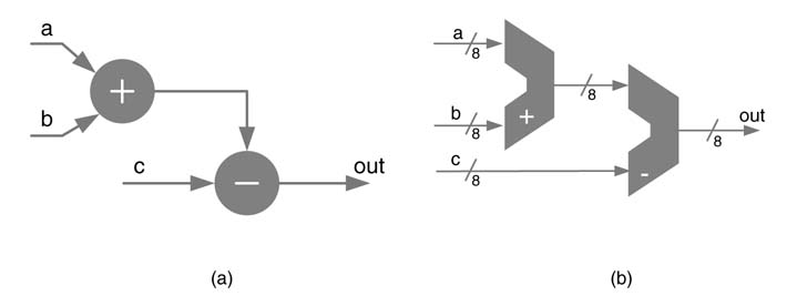
Example:Figure 9.1 shows the design of FDA, where we assume the sampling clock equals the circuit clock. The design is pipelined to increase the throughput performance of the architecture. A node-merging optimization technique is discussed in Chapter 5. The technique suggests the use of CSA and compression trees to minimize the use of CPA.
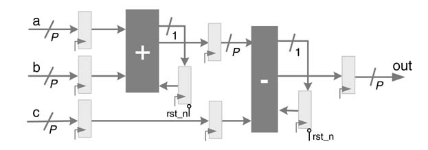
Now assume that for the DFG in Figure 9.1(a) the sampling clock frequency fess is eight times slower than the circuit clock frequency fact. This ratio implies the HW can be designed such that it can be shared eight times. While mapping the DFG for fact = 8fs, the design is optimized and transformed to a bit-serial architecture where operations are performed on bit-by-bit basis, thus effectively using eight clocks for every input sample. A pipelined bit-serial HW implementation of the algorithm is given in Figure 9.2, where for bit-serial design P = 1. The design consists of one full adder (FA) and a full subtract or (FS) replacing the adder and subtract or of the FDA design. Associated with the FA and FS for 1-bit addition and subtraction are two flip-flops (FRS) that feed the previous carry and borrow back to the FA and FS for bit-serial addition and subtraction operations, respectively. The FRS is cleared at every eighth clock cycle when the new 8-bit data is input to the architecture. The sum from the FA is passed to the FS through the pipeline FF. The 1-bit wide data path does not require packing of intermediate bits for any subsequent calculations. Many algorithms can be transformed and implemented on bit-serial architectures.
Figure 9.1 (a) Algorithm requiring equal sampling and clock frequencies. (b) Mapping on FDA
It is interesting to note that the architecture of Figure 9.2 can be easily extended to a digit-serial architecture by feeding digits instead of bits to the design. The flip-flop for carry and borrow will remain the same, while the adder, subtract or and other pipeline registers will change to digit size. For example, if the digit size is taken as 4-bit (i.e. P = 4), the architecture will take two cycles to process two sets of 4-bit inputs, producing out [3:0] in the first cycle and then [7:4] in the second cycle.
9.2.2 Sequential Architecture
In many design instances the algorithm is so regular that hardware can be easily designed to sequentially perform each iteration on shared HW. The HW executes the algorithm like a software program, sequentially implementing one iteration of the algorithm in one clock cycle. This architecture results in HW optimization and usually requires a very simple controller. Those algorithms that easily map to sequential architecture can also be effectively parallelized. Systolic architecture can also be designed for optimized HW mapping [9].
Figure 9.2 Bit-serial and digit-serial architectures for the DFG in Figure 9.1(a)
Example:This example considers the design of a sequential multiplier. The multiplier multiplies two N-bit signed numbers aand binNcycles. In the first N—1 clock cycles the multiplier generates the ith partial product (PPi) for a × b(i)and adds its ith shifted version to a running sum. For sign by sign multiplication, the most significant bit (MSB) of the multiplier bhas negative weight; therefore the (N—1)th shifted value of the final PPN_1 for a × b(N—1) is subtracted from the running sum. After N clock cycles the running sum stores the final product ofaxboperation. The pseudo-code of this algorithm is:
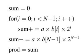
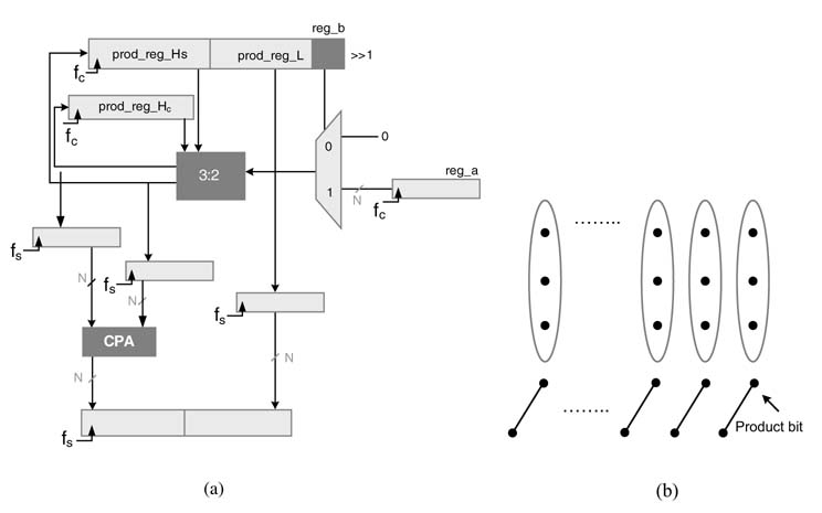
Figure 9.3 shows a hardware implementation of the (N × N)-bit sequential multiplier. The 2 N-bit shift register prod_reg is viewed as two concatenated registers: the register with N least significant bits (LBSs) is tagged as prod_reg_L, and the register with N MSBs is tagged as prod_reg_H, and for convenience of explanation this register is also named reg_b. Register reg_a in the design stores the multiplicand a.An N-bit adder/subtractor adds the intermediate PPs and subtracts the final PP from a running sum that is stored in prod_reg_L. The ith left shift of the PPi is successively performed by shifting the running sum in the prod_reg to the right in every clock cycle. Before starting the execution of sequential multiplication, reg_a is loaded with multiplicand a, prod_reg_H (reg_b) is loaded with multiplier b, and prod_reg_H is set to zero. Step-by-step working of the design is described below.
Figure 9.3 An N × N-bit sequential multiplier
S1 Load the registers with appropriate values for multiplication:
 prod_reg_H ! 0,
 reg_a ! multiplicand a,
 prod_reg_L (reg_b) ! multiplier b
S2 Each cycle adds the multiplicand to the accumulator if the ith bit of the multiplier is 1 and adds 0 when this bit is a 0:
if reg_b[i]==1 then
 prod_reg_H += reg_a
else
 prod_reg_H+=0
In every clock cycle, prod_reg is also shifted right by 1. For sign by sign multiplication, right shift is performed by writing back the MSB of prod_reg to its position while all the bits are moved to the right. For unsigned multiplication, a logical right shift by 1 is performed in each step.
S3 For signed multiplication, in the Nth clock cycle, the adder/subtractor is set to perform subtraction, whereas for unsigned multiplication addition is performed in this cycle as well.
S4 After N cycles, prod_reg stores the final product.
A multiplexer is used for the selection of contents of reg_a or 0. The LSB of reg_b isused for this selection. This is a good example of time-shared architecture that uses an adder and associated logic to perform multiplication in N clock cycles.
The architecture can be optimized by moving the CPA out from the feedback loop, as in Figure 9.4(a). The results of accumulation are saved in a partial sum and carry form in prod_reg_Hs and prod_reg_Hc, respectively. The compression tree takes the values saved in these two registers and the new PPi and compresses them to two layers. This operation always produces one free product bit, as shown in Figure 9.4(b). The compressed partial sum and carry are saved one bit position to the right. In N clock cycles the design produces N product Labs, whereas N product MSBs in sum and carry form are moved to a set of registers clocking at slower clock fess and are then added using a CPA working at slower clock speed. The compression tree has only one full adder Delay and works at faster clock speed, allowing the design to work in high-performance applications.
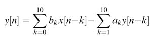
Example: A sequential implementation of a 5-coefficient FIR filter is explained in this example. The filter implements the difference equation:
For the sequential implementation, let us assume that fact is five times faster than fess. This implies that after sampling an input value at fess the design running at clock frequency fact has five clock cycles to compute one output sample. An FDA implementation will require five multipliers and four adders. Using this architecture, the design running at fact would compute the output in one clock cycle and would then wait four clock cycles for the next input sample. This obviously is a waste of resources, so a time-shared architecture is preferred.
Figure 9.4 Optimized sequential multiplier. (a) Architecture using a 3:2 compression tree and CPA operating at fact and fess. (b) Compression tree producing one free product bit
A time-shared sequential architecture implements the same design using one MAC (multiplier and accumulator) block. The pseudo-code for the sequential design implementing (9.1) is:
The design is further optimized by moving the CPA out of the running multiplication and accumulation operation. The results from the compression tree are kept in partial sum and carry form in two sets of accumulator registers, accs and accc, and the same are fed back to the compression tree for MAC operation. The partial results are moved to two registers clocked at slower clock fess. The CPA adds the two values at slower clock fess. The pseudo-code for the optimized design is:
A generalized hardware design for an N-coefficient FIR filter is shown in Figure 9.5. The design assumes cuffs = N. The design has a tap Delay line that samples new input data at every clock fess at the top of the line and shifts all the values down by one register. The coefficients are either saved in ROM, or registers may also be used if the design is required to work for adaptive or changed coefficients. A new input is sampled in register x_n the tap Delay line of the design, and accs and accc are reset. The design computes one output sample in N clock cycles. After N clock cycles, a new input is sampled in the tap Delay line and partial accumulator registers are saved in intermediate registers clocked at fess. The registers are initialized in the same cycle for execution of the next iteration. A CPA working at slower clock fess adds the sum of partial results in the intermediate registers and produces yen.
Figure 9.5 Time-shared N-coefficient FIR filter
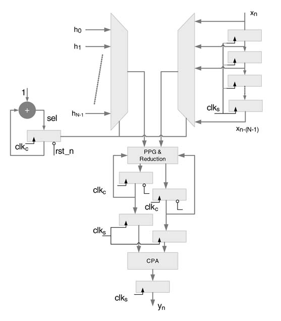
The HW design assumes that the sampling clock is synchronously derived from the circuit clock. The shift registers storing the current and previous input samples are clocked using the sampling clock clks, and so is the final output register. At every positive edge of the sampling clock, each register stores a new value previously stored in the register located above it, with the register at the top storing the new input sample. The data path executes computation on the circuit clock clkc, which are N times faster than the sampling clock. The top-level design consisting of data path and controller is depicted in Figure 9.6. The controller clears the partial sum and carry registers and starts generating the select signals Sel_h and sel_l for the two multiplexers, starting from 0 and then incrementingby1ateverypositive edge of clkc.At the Nth clock cycle the final output is generated, and the controller restarts again to process a new input sample.
Figure 9.6 Datapath and controller of FIR filter design
9.3 Sequencing and Control
In general, a time-shared architecture consists of a data path and a control unit. The datapath is the computational engine and consists of registers, multiplexers, de-multiplexers, ALUs, multipliers, shifters, combinational circuits and buses. These HW resources are shared across different computations of the algorithm. This sharing requires a controller to schedule operations on sets of operands. The controller generates control signals for the selection of these operands in a predefined sequence. The sequence is determined by the dataflow graph or flow of the algorithm. Some of the operations in the sequence may depend on results from earlier computations, so status signals are fed back to the control unit. The sequence of operations may also depend on input signals from other modules in the system.
Figure 9.7 shows these two basic building blocks. The control unit implements the schedule of operations using a finite state mMachine.
9.3.1 Finite State Machines
A synchronous digital design usually performs a sequence of operations on the data stored in registers and memory of its datapath under the direction of a finite state machine (FSM). The FSM is a sequential digital circuit with an N-bit state register for storing the current state of the sequence of operations.An N-bit state register can have 2N possiblevalues, sothe number of possible states in the sequence is finite. The FSM can be described using a bubble (state) diagram or an algorithmic state machine (ASM) chart.
Figure 9.7shows these two basic building blocks. The control unit implements the schedule of operations using a finite state mMachine.
Figure 9.8 Combinational and sequential components of an FSM design
FSM implementation in hardware has two components, a combinational cloud and a sequential logic. The combination cloud computes the output and the next state based on the current state and input, whereas the sequential part has the reset able state register. A FSM with combinational and sequential components is shown in Figure 9.8.
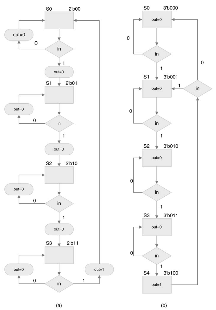
Example: This example designs an FSM that counts four 1s on a serial interface and generates a 1 at the output. One bit is received on the serial interface at every clock cycle. Figure 9.9 shows a bubble diagram in which each circle represents a state, and lines and curves with arrowheads represent state transitions. There are a total of four states, S0... S3.
S0 represents the initial state where number of 1s received on the interface is zero. A 0/0 on the transition curve indicates that, in state S0, if the input on the serial interface is 0 then the state machine maintains its state and generates a 0 at the output. In the same state S0, if 1 is received at the input, the FSM changes its state to S1 and generates a 0 at the output. This transition and input-output relationship is represented by 1/0 on the line or curve with an arrowhead showing state transition from state S0 to S1. There is no change in state if the FSM keeps receiving 0s in the S1 state. This is represented by 0/0 on the state transition curve on S1. If it receives a 1 in state S1 it transitions to S2. The state remains S2 if the FSM in S2 state keeps receiving zeros, whereas another 1 at the input causes it to transition to state S3. In state S3, if the FSM receives a 1 (i.e. the fourth 1), the FSM generates a 1 at the output and transitions back to initial state S0 to start the counting again. Usually a state machine may be reset at any time and the FSM transitions to state S0.
Figure 9.9 State diagram implementing counting of four 1s on a serial interface
9.3.2 State Encoding: One-hot versus Binary Assignment
There are various ways of coding the state of an FSM. The coding defines a unique sequence of numbers to represent each state. For example, in a ‘one-hot’ state machine with N states there are N bits to represent these states. An isolated 1 at a unique bit location represents a particular state of the machine. This obviously requires an N-bit state register. Although a one-hot state machine results in simple logic for state transitions, it requires N flip-flops as compared to log2N in a binary-coded design. The latter requires fewer flip-flops to encode states, but the logic that decodes the states and generates the next states is more complex in this style of coding.
The arrangement with a one-hot state machine, where each bit of the state register represents a state, works well for FPGA-based designs that are rich in flip-flops. This technique also avoids large fa N-outs of binary-coded state registers, which does not synthesize well on FPGAs.
A variant, called ‘almost one-hot’, can be used for state encoding. This is similar, with the exception of the initial state that is coded as all zeros. This helps in easy resetting of the state register. In another variant, two bits instead of one are used for state coding.
For low-power designs the objective is to reduce the hamming distance among state transitions. This requires the designer to know the statistically most probable state transition pattern. The pattern is coded using the gray codes. These four types of encoding are given in Table 9.1.
If the states in the last example are coded as a one-hot state machine, for four states in the FSM, a state register of size 4 will be used where each flip-flop of the register will be assigned to one state of the FSM.
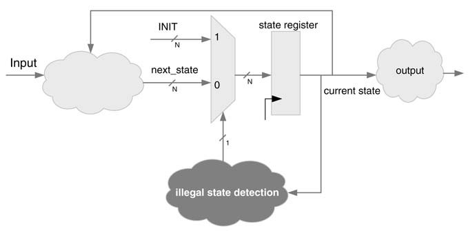
As a consequence of one-hot coding, only one bit of the state register can be 1 at any time. The designer needs to handle illegal states by checking whether more than one bitofthestate registeris1. In many critical designs this requires exclusive logic that, independently of the state machine, checks whether the state machine is in an illegal state and then transitions the state machine to the reset state. Using N flip-flops to encode a state machine with N states, there will bea total of 2 N – N illegal states. These need to be detected when, for example, some external electrical phenomenon takes the state register to an illegal state. Figure 9.10 shows an FSM with one-hot coding and an exclusive logic for detecting illegal states. If the state register stores an illegal state, the FSM is transitioned to initial state INIT.
Table 9.1 State encoding techniques
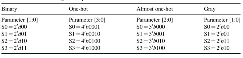
Figure 9.10 One-hot state machine with logic that detects illegal states
FPGA synthesis tools facilitate the coding of states toone-hot orbinary encoding. This is achieved by selecting the appropriate encoding option in the FPGA synthesis tool.
9.3.3 Mealy and Moore State Machine Designs
In a Mealy machine implementation, the output of the FSM is a function of both the current state and the input. This is preferred in applications where all the inputs to the FSM are registered outputs from some other blocks and the generation of the next state and FSM output are not very complex. It results in simple combinational logic with a short critical path.
In cases where the input to the FSM is asynchronous (it may change within one clock cycle), the FSM output will also be asynchronous. This is not desirable especially in designs where outputs from the FSM are the control signals to the datapath. The datapath computational units are also combinational circuits, so an asynchronous control signal means that the control may not be stable for one complete clock cycle. This is undesirable as the datapath expects all control signals to be valid for one complete clock cycle.
In designs where the stability of the output signal is not a concern, the Mealy machine is preferred as it results in fewer states. A Mealy machine implementation is shown in Figure 9.11. The combinational cloud computes the next state and the output is based on the current state and the input. The state register has an asynchronous reset to initialize the FSM at any time if desired.
Figure 9.11 Composition of a Mealy machine implementation of an FSM
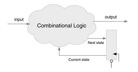
Figure 9.12 Composition of a Moore machine implementation of an FSM
In a Moore machine implementation, outputs are only a function of the current state. As the current sate is registered, output signals are stable for one complete clock cycle without any glitches. In contrast to the Mealy machine implementation, the output will be Delayed by one clock cycle. The Moore machine may also result in more states as compared to the Mealy machine.
The choice between Mealy and Moore machine implementations is the designer’s and is independent of the design problem. In many design instances it is a fairly simple decision to select one of the two options. In instances where some of the inputs are expected to glitch and outputs are required to be stable for one complete cycle, the designer should always use the Moore machine.
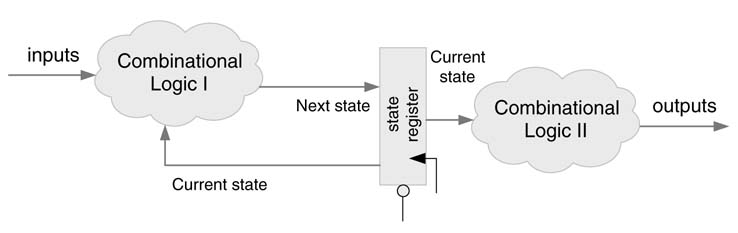
A Moore machine implementation is shown in Figure 9.12. The combinational logic-I of the FSM computes the next state based on inputs and the current state, and the combinational logic-II of the FSM computes the outputs based on the current state.
9.3.4 Mathematical Formulations
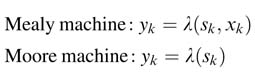
Mathematically an FSM can be formulated as a sextuple, ( X, Y, S, s0, δ, λ), where X and Y are sets of inputs and outputs, S is set of states, s0 is the initial state, and δ and λ are the functions for computing the next state and output, respectively. The expression for next state computation can be written as:
Subscript k is the time index for specifying the current input and current state, so using this notation sk+1 identifies the next state. For Mealy and Moore machines the expressions for computing output can be written as:
9.3.5 Coding guidelines for Finite State Machines
Efficient hardware implementation of a finite state machine necessitates adhering to some coding guidelines [10, 11].
9.3.5.1 Design Partitioning in Datapath and Controller
The complete HW design usually consists of a datapath and a controller. The controller is implemented as an FSM. From the synthesis perspective, the datapath and control parts have different design objects. The datapath is usually synthesized for better timing whereas the controller is synthesized to take minimum area. The designer should keep the FSM logic and datapath logic in separate modules and then synthesize respective parts selecting appropriate design objectives.
9.3.5.2 FSM Coding in Procedural Blocks
The logic in an FSM module is coded using one or two always blocks. Two always blocks are preferred, where one implements the sequential part that assign the next state to the state register, and the second block implements the combinational logic that computes the next state Sk+1 = ´(ax, Ski). The designer can include the output computations yak = ( Ski, ax) or yak = »( Ski) for Mealy or Moore machines, respectively, in the same combinational block. Alternatively, if the output is easy to compute, they can be computed separately in a continuous assignment outside the combinational procedural block.
9.3.5.3 State Encoding
Each state in an FSM is assigned a code. From the readability perspective the designer should use meaningful tags using 'define or parameter statements for all possible states. Use of parameter is preferred because the scope of parameter is limited to the module in which it is defined whereas ‘define is global in scope. The use of parameter enables the designer to use the same state names with different encoding in other modules.
Based on the design under consideration, the designer should select the best encoding options out of one-hot, almost one-hot, gray or binary. The developer may also let the synthesis tool encode the states by selecting appropriate directives. The Synopsis tool lets the user select binary, one-hot or almost one-hot by specifying it with the parameter declaration. Below, binary coding is invoked using the enum synopsis directive:
parameter [3:0] // Synopsys enema code
9.3.5.4 Synthesis Directives
In many designs where only a few of the possible states of the state register are used, the designer can direct the synthesis tool to ignore unused states while optimizing the logic. This directive for Synopsys is written as:
case(state) // Synopsys full case
Adding //Synopsis full_case to the case statement indicates to the synthesis tool to treat all the cases that are explicitly not defined as ‘don’t care’ for optimization. The designer knows that undefined cases will never occur in the design. Consider this Example:
always @* begin
case (centre) // Synopsys full case
 2’b00: out = in1;
 2’b01: out = in2;
 2’b10: out = in3;
endcase
The user controls the synthesis tool by using the directive that the cntr signal will never take the unused value 2' b11. The synthesis tool optimizes the logic by considering this case as ‘don’t care’.
Similarly, //Synopsis parallel_case is used where all the cases in a case, casex or casez statement are mutually exclusive and the designer would like them tobe evaluate dinparallel or the order in which they are evaluated does not matter. The directive also indicates that all cases must be individually evaluated in parallel:
always @* begin
// Code for setting the output to default comes here
casez (intr_req) // Synopsys parallel_case
3’b??1:
begin // Check bit 0 while ignoring rest
 // Code for interrupt 0 comes here
end
3’b?1?:
begin // Check bit 1 while ignoring rest
 // Code for interrupt 1 comes here
end
3’b??1:
begin // Check bit 2 while ignoring rest
 // Code for interrupt 2 comes here
end
endcase
The onus is on the designer to make sure that no two interrupts can happen at the same time. On this directive, the synthesis tool optimizes the logic assuming no N-overlapping cases.
While using one-hot or almost one-hot encoding, the use of //Synopsys full_case_ parallel_case signifiesthat all the cases are no N-overlapping and only one bit of the state register will be set and the tool should consider all other bit patterns of the state register as ‘don’t care’. This directive generates the most optimal logic for the FSM.
Instead of using the default statement, it is preferred to use parallel_case and full_ case directives for efficient synthesis. The default statement should be used only in simulation and then should be turned off for synthesis using the compiler directive. It is also important to know that these directives have their own consequences and should be cautiously use in the implementation.
Example: Using the guidelines, RTL Verilog code to implement the FSM of Figure 9.9 is given below. Listed first is the design using binary encoding, where the output is computed inside the combinational block:
// This module implements FSM for the detection of
// four ones in a serial input stream of data
module fsm_mealy(
 input clk, //system clock
 input reset, //system reset
 input data_in, //1-bit input stream
 output regfour_ones_det //1-bitoutputtoindicate 4onesaredetectedornot
 );
// Internal Variables
 reg [1:0] current_state, //4-bit current state register
 next_state; //4-bit next state register
// State tags assigned using binary encoding
parameter STATE_0 = 2’b00,
 STATE_1 = 2’b01,
 STATE_2 = 2’b10,
 STATE_3 = 2’b11;
// Next State Assignment Block
// This block implements the combination cloud of next state assignment logic
always @(*)
begin: next_state_bl
 case(current_state)
 STATE_0:
 begin
 if(data_in)
 begin
 //transition to next state
 next_state = STATE_1;
 four_ones_det = 1’b0;
 end
 else
 begin
 //retain same state
 next_state = STATE_0;
 four_ones_det = 1’b0;
 end
 end
 STATE_1:
 begin
 if(data_in)
 begin
 //transition to next state
 next_state = STATE_2;
 four_ones_det = 1’b0;
 end
 else
 begin
 //retain same state
 next_state = STATE_1;
 four_ones_det = 1’b0;
 end
 end
 STATE_2:
 begin
 if(data_in)
 begin
 //transition to next state
 next_state = STATE_3;
 four_ones_det = 1’b0;
 end
 else
 begin
 //retain same state
 next_state = STATE_2;
 four_ones_det = 1’b0;
 end
 end
 STATE_3:
 begin
 if(data_in)
 begin
 //transition to next state
 next_state = STATE_0;
 four_ones_det = 1’b1;
 end
 else
 begin
 //retain same state
 next_state = STATE_3;
 four_ones_det = 1’b0;
 end
 end

 endcase
end

 // Current Register Block
 always @(posedge clk)
 begin: current_state_bl

 if(reset)
 current_state <= #1 STATE_0;
 else
 current_state <= #1 next_state;
 end
end module
The following codes the same design using one-hot coding and computes the output in a separate continuous assignment statement. Only few states are coded for demonstration. For effective HW mapping, aninverse case statement is used where each case is only evaluated to be TRUE or FALSE:
always@(*)
begin
next_state = 4’b0;
case (1’b1) // Synopsys parallel_case full_case
 current_state[S0]:
 if (in)
 next_state[S1] = 1’b1;
 else
 next_state[S0] = 1’b1;
 current_state[S1]:
 if (in)
 next_state[S2] = 1’b1;
 else
 next_state[S1] = 1’b1;
 endcase
 end
// Separately coded output function
assign output = state[S3];
9.3.6 SystemVerilog Support for FSM Coding
Chapter 3 gives an account of SystemVerilog. The language supports multiple procedural blocks such as always comb, always_ff and always_latch, along with unique and priority keywords. The directives of full_case, parallel_case and full_case_ parallel_case are synthesis directives and are ignored by simulation and verification tools. There may be instances when the wrong designer perception can go unchecked. To cover these short comings, SystemVerilog supports these statements and keywords to provide unified behavior in simulation and synthesis. The statements cover all the synthesis directives and the user can appropriately select the statements that are meaningful for the design. These statements ensure coherent behavior of the simulation and post-synthesis code [27].
Example: The compiler directives are ignored by simulation tools. Use of the directives may create mismatches between pre- and post-synthesis results. The following example of a Verilog implementation explains how SystemVerilog covers these short comings:
always@(cntr, in1, in2, in3, in4)
casex (cntr) /* Synopsys full_case parallel_case */
 4’b1xxx: out = in1;
 4’bx1xx: out = in2;
 4’bxx1x: out = in3;
 4’bxxx1: out = in4;
endcase
As the simulator ignores the compiler directives, a mismatch is possible when more than two bits of cntr are 1 at any time. The code can be rewritten using SystemVerilog for better interpretation:
always_comb
unique casex (cntr)
 4’b1xxx: out = in1;
 4’bx1xx: out = in2;
 4’bxx1x: out = in3;
 4’bxxx1: out = in4;
endcase
In this case the simulator will generate a warning if the cntr signal takes values that are not one-hot. This enables the designer to identify problems in the simulation and functional verification stages of the design cycle.
9.4 Algorithmic State Machine Representation
9.4.1 Basics
Hardware mapping of signal processing and communication algorithms is the main focus of this book. These algorithms are mostly mapped on time-shared architectures. The architectures require the design of FSMs to generate control signals for the datapath. In many designs the controllers have algorithm-like functionality. The functionality also encompasses decision support logic. Bubble diagrams are not flexible enough to describe the complex behavior of these finite state machines. Furthermore, many design problems require gradual refinement and the bubble diagram representation is not appropriate for this incremental methodology. The bubble diagram is also not algorithm-like. The algorithmic state machine (ASM) notation is the representation of choice for these design problems.
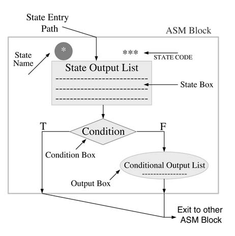
ASM is a flowchart-like graphical notation that describes the cycle-by-cycle behavior of an algorithm. Each step transitioning from one state to another or to the same state takes one clock cycle. The ASMis composed of three basic building blocks: rectangles, diamonds and ovals. Arrows are used to interconnect these building blocks. Each rectangle represents a state and the state output is written inside the rectangle. The state output is always an unconditional output, which is asserted when the FSM transitions to a state represented by the respective rectangle. A diamond is used for specifying a condition. Based on whether the condition is TRUE or FALSE, the next state or conditional output is decided. An oval is used to represent a conditional output. As Moore machines only have state outputs, Moore FSM implementations do not have ovals, but Mealy machines may contain ovals in their ASM representations.Figure 9.13 shows the relationship of three basic components in an ASM representation. For TRUE or FALSE, T and F are written on respective branches. The condition may terminate in an oval, which lists conditional output.
Figure 9.13 Rectangle, diamond and oval blocks in an ASM representation
The ASM is very descriptive and provides a mechanism fora systematic and step-by-step design of synchronous circuits. Once defined it can be easily translated into RTL Verilog code. Many off-the-shelf tools are available that directly convert an ASM representation into RTL Verilog code [11].
Example: Consider the design of Figure 9.9. The FSM implements counting of four 1s on a serial interface using Mealy or Moore machines. This example describes the FSM using ASM representation. Figure 9.14 shows the representations. The Moore machine requires an additional state.
9.4.2Example: Design of a Four-entry FIFO
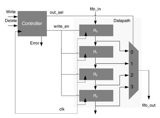
Figure 9.15 shows the datapath and control unit for a 4-entry FIFO queue. The inputs to the controller are two operations, Write and Del. The former moves data from the fifo_in to the tail of the FIFO queue, and the latter Deletes the head of the queue. The head of the queue is always available at fifo_out. A Write into a full queue or Deletion from an empty queue causes an error condition. Assertion of Write and Del at the same time also causes an error condition.
The datapath consists of four registers, R0, R1, R2 and R3, and a multiplexer to select the head of the queue. The input to the FIFO is stored in R0 when the Write_en is asserted. The Write_en also moves the other entries in the queue down by one position. With every new Write and Delete in the queue, the controller needs to select the head of the queue from its new location using an out_sel signal to the multiplexer. The FSM controller for the datapath is described using an ASM chart in Figure 9.16.
The initial state of FSM is S0 and it identifies the status of the queue as empty. Any Del request to an empty queue will cause an error condition, as shown in the ASM chart. On a Write request the controller asserts a Write_en signal and the value at fifo_in is latched in register R0. The controller also selects R0 at the output by assigning value 3' b00 to out_sel. On a Write request the controller also transitions to state S1. When the FSMisin S1 a Del takes the FSM backto S0 and a Write takes it to S2. Similarly, another Write in state S2 transitions the FSM to S3. In this state, another Write generates an error as the FIFO is now completely filled. In every state, Write and Del at the same time generates an error.
Partial RTLVerilog code of the datapath and the FSM is given below. The code only implements state S0. All the other states can be easily coded by following the ASM chart of Figure 9.16.
// Combinational part only for S0 and default state is given
always @(*)
begin
 next_state=0;
 case(current_state)

 `S0:
 begin
 if(!Del&&Write)
 begin
 next_state = `S1;
 Write_en = 1’b1;
 Error= 1’b0;
 out_sel = 0;
 end
 else if(Del)
 begin
 next_state=`S0;
 Write_en =1’b0;
 Error = 1’b1;
 out_sel=0;
 end
 else
 begin
 next_state=`S0;
 Write_en=1’b0;
 out_sel = 1’b0;
 end

 // Similarly, rest of the states are coded //

 default:
 begin
 next_state=`S0;
 Write_en = 1’b0;
 Error = 1’b0;
 out_sel =0;
 end
 endcase
end
// Sequential part
always @(posedge clk or negedge rst_n)
if(!rst_n)
 current_state <= #1’S0;
else
 current_state <= #1 next_state;
Figure 9.14 ASM representations of four 1s detected problem of Figure 9.9: (a) Mealy machine; (b) Moore machine
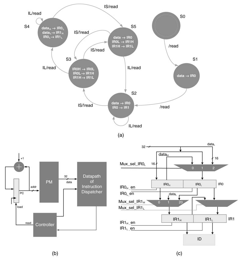
9.4.3Example: Design of an Instruction Dispatcher
This section elaborates the design of an FSM-based instruction dispatcher for a programmable processor that can read 32-bit words from program memory (PM). The instruction words are written into two 32-bit instruction registers, IR0 and IR1. The processor supports short and long instructions of lengths 16 and 32-bit, respectively. The LSB of the instruction is coded to specify the instruction type. A 0 in the LSB indicates a 16-bit instruction and a 1 depicts the instruction is 32-bit wide. The dispatcher identifies the instruction type and dispatches the instruction to the respective Instruction Decoder (ID).
Figure 9.17(a) shows the bubble diagram that implements the instruction dispatcher. Following is the description of the working of the design.
1. The dispatcher’s reset state is S0.
2. The FSM reads the first 32-bit word from PM, transitions into state S1 and stores it in instruction register IR0.
3. The FSM then reads another 32-bit word, which is latched inIR0 while it shifts the contents ofIR0 to IR1 in the same cycle and makes transitions from S1 to S2. In state S2 the FSM reads the LSB of IR1 to check the instruction type. If the instruction is of type long (IL) i.e. 32-bit instruction it is dispatched to the IDfor long instruction decoding and another 32-bit word is read inIR0 where the contents of IR0 are shifted to IR1. The FSM remains in state S2. On the other hand, if the FSMis in state S2 and the current instruction is of type short (IS), then the instruction is dispatched to the Instruction Decoder Short (IDS) and the FSM transition into S3 without performing any read operation
Figure 9.15 Four-entry FIFO queue with four registers and a multiplexer in the datapath
4. In state S3, the FSM readjusts data. IR1H representing 16 MSBs of register IR1 is moved to IR1L that depicts 16 LSBs of the instruction register IR1. In the same sequence of operations, IR0H and IR0L are moved to IR0L and IR1L, respectively. In state S3, the FSM checks the instruction type. If the instruction is of type long the FSM transitions to state S4; otherwise if the instruction is of type short the FSM transitions to S5.In both cases FSM initiates a new read from PM.
5. The behavior of the FSM in states S4 and S5 is given in Figure 9.17(a). To summarize, the FSM adjusts the data in the instruction registers such that the LSB of the current instruction is in the LSB of IR1 and the dispatcher brings the new 32-bit data from PM in IR0 if required. Figure 9.17(b) shows the associated architecture for readjusting the contents of instruction registers. The control signals to multiplexers are generated to bring the right inputs to the four registers IR0H, IR0L, IR1H and IR1L for latching in the next clock edge.
The RTL Verilog code of the dispatcher is given here:
// Variable length instruction dispatcher moduleVariableInstructionLengthDispatcher(inputclk,rst_n,output[31:0]IR1);
reg [31:0] program_mem [0:255];
reg [7:0] PC; // program counter for memory (physical reg)
wire [15:0] data_H; // contains 16 MSBs of data from program memory
wire [15:0] data_L; // contains 16 LSBs of data from program_mem
reg [5:0] next_state, current_state;
reg read;
reg IR0_L_en, IR0_H_en; // Write enable for IR0 regsiter
reg [1:0] mux_sel_IRO_L;
reg IR1_L_en, IR1_H_en; // Write enable for IR1 register
reg [1:0] mux_sel_IR1_H;
reg mux_sel_IR1_L;
reg [15:0] mux_out_IR0_L, mux_out_IR1_H, mux_out_IR1_L;
reg [15:0] IR0_H, IR0_L, IR1_H, IR1_L;
// state assignments parameter [5:0] S0 = 1; parameter [5:0] S1 = 2; parameter [5:0] S2 = 4; parameter [5:0] S3 = 8; parameter [5:0] S4 = 16; parameter [5:0] S5 = 32;
// loading memory "program_memory.txt"
initial
begin
$readmemh("program_memory.txt",program_mem); end
assign {data_H, data_L} = program_mem[PC];
assign IR1 = {IR1_H, IR1_L}; //instructions in IR1 get dispatched
always @ (*) begin
// default settings next_state = 6’d0; read = 0;
IR0_L_en = 1’b0; IR0_H_en = 1’b0; // disable registers
mux_sel_IRO_L = 2’b0;
IR1_L_en = 1’b0; IR1_H_en = 1’b0;
mux_sel_IR1_H = 2’b0;
mux_sel_IR1_L = 1’b0;
case (current_state)
S0:
begin
read=1’b1; next_state = S1;
IR0_L_en = 1’b1; IR0_H_en = 1’b1; // load 32 bit data from PM into the IR0 register
mux_sel_IRO_L = 2’d2; end
S1: begin
read = 1’b1; next_state = S2; IR0_L_en = 1’b1; IR0_H_en = 1’b1; // load 32 bit data from PM into the IR0 register
mux_sel_IRO_L = 2’d2;
IR1_L_en = 1’b1; IR1_H_en = 1’b1; // load the contents of IR0 in IR1 (full 32bits)
mux_sel_IR1_H = 2’d0;
mux_sel_IR1_L = 1’b1; end
S2:
begin
if (IR1_L[0]) begin
read=1’b1; next_state = S2;
IR0_L_en = 1’b1; IR0_H_en = 1’b1; the IR0 register
mux_sel_IRO_L = 2’d2; IR1_L_en = 1’b1; IR1_H_en = 1’b1 IR1 (full 32bits)
mux_sel_IR1_H = 2’d0; mux_sel_IR1_L = 1’b1; end else begin
read=1’b0; next_state = S3; IR0_L_en = 1’b1; IR0_H_en = 1’b0; mux_sel_IRO_L = 2’d0; IR1_L_en = 1’b1; IR1_H_en = 1’b1 IR1_H –> IR1_L
mux_sel_IR1_H = 2’d2; mux_sel_IR1_L = 1’b0; end end
S3:
begin if (IR1_L[0]) begin read=1’b1; next_state = S4;
IR0_L_en = 1’b1; IR0_H_en = 1’b0; mux_sel_IRO_L = 2’d1; IR1_L_en = 1’b1; IR1_H_en = 1’b1; mux_sel_IR1_H = 2’d1; mux_sel_IR1_L = 1’b1; end else begin
read = 1’b1;
next_state = S5; IR0_L_en = 1’b1; IR0_H_en = 1’b1; the IR0 register
mux_sel_IRO_L = 2’d2;
IR1_L_en = 1’b1; IR1_H_en = 1’b1; IR1_H –> IR1_L
mux_sel_IR1_H = 2’d2;
mux_sel_IR1_L = 1’b0;
// instruction type: long
// load 32 bit data from PM into // load the contents of IR0 in
// move IR0_H –> IR0_L; // move IR0_L –> IR1_H and
// instruction type: long
// move dataH –> IR0_L
// move dataL –> IR1_H // move IR0_L –> IR1_L
// instruction type: short
// no read
// load 32 bit data from PM into
// move IR0_L –> IR1_H and
// instruction type: long
end end
S4:
begin
if (IR1_L[0]) begin read=1’b1; next_state = S4;
IR0_L_en = 1’b1; IR0_H_en = 1’b0;
mux_sel_IRO_L = 2’d1;
IR1_L_en = 1’b1; IR1_H_en = 1’b1;
mux_sel_IR1_H = 2’d1;
mux_sel_IR1_L = 1’b1;
end
else
begin
read = 1’b1; next_state = S5; IR0_L_en = 1’b1; IR0_H_en = 1’b1; the IR0 register
mux_sel_IRO_L = 2’d2; IR1_L_en = 1’b1; IR1_H_en = 1’b IR1_H –> IR1_L
mux_sel_IR1_H = 2’d2; mux_sel_IR1_L = 1’b0; end end
S5: begin
if (IR1_L[0]) begin read=1’b1; next_state = S2; IR0_L_en = 1’b1; IR0_H_en = 1’b1; the IR0 register
mux_sel_IRO_L = 2’d2; IR1_L_en = 1’b1; IR1_H_en = 1’b1; in IR1 (full 32bits)
mux_sel_IR1_H = 2’d0; mux_sel_IR1_L = 1’b1; end
else begin
read=1’b0;
next_state = S3; IR0_L_en = 1’b1; IR0_H_en = 1’b0;
mux_sel_IRO_L = 2’d0;
IR1_L_en = 1’b1; IR1_H_en = 1’b1;
// move dataH –> IR0_L
// move dataL –> IR1_H // move IR0_L –> IR1_L
// instruction type: short
// no read
// load 32 bit data from PM into
// move IR0_L –> IR1_H and
// instruction type: long
// load 32 bit data from PM into // load the contents of IR0
// instruction type: short
// move IR0_H –> IR0_L; // move IR0_L –> IR1_H and
IR1_H –> IR1_L
mux_sel_IR1_H = 2’d2; mux_sel_IR1_L = 1’b0; end end endcase end
always @ (*) begin
mux_out_IR0_L = 16’bx; case (mux_sel_IRO_L)
2’b00: mux_out_IR0_L = IR0_H; 2’b01: mux_out_IR0_L = data_H; 2’b10: mux_out_IR0_L = data_L; endcase end
always @ (*) begin
mux_out_IR1_H = 16’bx; case (mux_sel_IR1_H)
2’b00: mux_out_IR1_H = IR0_H; 2’b01: mux_out_IR1_H = data_L; 2’b10: mux_out_IR1_H = IR0_L; endcase end
always @ (*) if(mux_sel_IR1_L)
mux_out_IR1_L = IR0_L; else
mux_out_IR1_L = IR1_H;
always @ (posedge clk or negedge rst_n) begin
if (!rst_n) begin
PC <= 8’b0;
current_state <= 6’b000_001; end else begin
current_state <= next_state; if (read)
PC <= PC+1; end
// if enable load Instruction registers with valid values if (IR0_H_en)
IR0_H <= data_H; if (IR0_L_en)
IR0_L <= mux_out_IR0_L;
if (IR1_H_en)
IR1_H <= mux_out_IR1_H; if (IR1_L_en)
IR1_L <= mux_out_IR1_L;
end endmodule
Figure 9.16 FSM design of 4-entry FIFO queue using ASM chart
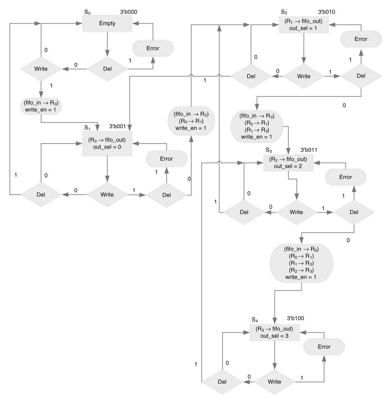
Figure 9.17 FSM implementing a variable-length instruction dispatcher. (a) Bubble-diagram representation of the FSM. (b) Architecture consisting of PM, PC, datapath and controller. (c) Datapath of the instruction dispatcher
9.5 FSM Optimization for Low Power and Area
There are a number of ways to implement an FSM. The designer, based on some set design objectives, selects one out of many options and then the synthesis tool further optimizes an FSM implementation [12, 13]. The tool, based on a selected optimization criterion, transforms a given FSM to functionally equivalent but topologically different FSMs. Usually FSMs are optimized for power and area. the many available optimization algorithms, one is to find a critical state that is connected to many states where the transitions into the critical state cause large hamming distances, thus generating significant switching activity. The algorithm, after identifying the critical state, splits it into two to reduce the hamming distance among the connected states and then analyzes the FSM to evaluate whether the splitting results in a power reduction without adding too much area in the design.
The dynamic power dissipation in digital logic depends on switching activity. The tools, while performing state minimization for area reduction, also aim to minimize total switching activity. Out of
Figure 9.18 FSM optimization by splitting a critical state to reduce the hamming distance of state transitions. (a) Portion of original FSM with critical state. (b) Splitting of critical state into two
This is illustrated in Figure 9.18. Part (a) shows the original FSM, and (b) shows the transformed FSM with reduced switching activity as a result of any transition into the states formed by splitting the critical state. In an FSM with a large number of states, modeling the problem for an optimal solution is an ‘NP complete’ problem. Several heuristics are proposed in the literature, and an effective heuristic for the solution is given in [16].
9.6 Designing for Testability
From the testability perspective it is recommended to add reset and status reporting capabilities in an FSM. To provide an FSM with a reset capability, there should be an input that makes the FSM transition from any state to some defined initial state. An FSM with status message capability also increases the testability of the design. An FSM with this capability always returns its current state for a defined query input.
9.6.1 Methodology
The general methodology of testing digital designs discussed in Chapter 2 should be observed. Additionally, the methodology requires a specification or design document of the FSM that completely defines the FSM behavior for all possible sequences of inputs. This requires the developer to generate minimum length sequences of operations that must test all transitions of the FSM.
For initial white-box module-level testing, the stimulus should keep a record of all the transitions, corresponding internal states of the FSM, and inputs and output before a fault appears. This helps the designer to trace back and localize a bug.
For a sequence of inputs, using the design specification, the designer needs to find the corresponding sequence of outputs for writing test cases. A test case then checks whether the FSM implementation conforms to the given set. The designer should find a minimum number of shortest possible length sequences that check every possible transition. Various coverage measures are used for evaluating the completeness of testing. Various coverage tools are also available that the designer can easily adopt and integrate with the RTL flow. The tools help the designer to identify unverified areas of the FSM implementation. The designer then needs to generate new test cases to verify those areas. A brief discussion of these measures is given here.
9.6.2 Coverage Metrics for Design Validation
9.6.2.1 Code Coverage
The simplest of all the metrics is code coverage that validates that every line of code is executed at least once. This is very easy to verify as most of the simulators come with inbuilt profilers. Though 100% line coverage is a good initial measure, this type of coverage is not a good enough indicator of quality of testing and so must be augmented with other more meaningful measures.
9.6.2.2 Toggle Coverage
This measure checks whether every bit in all the registers has at least toggled once from 0 to 1 and 1 to 0. This is difficult to cover, as the content of registers are the outcome of some complex functions. The tester usually does not have deep enough understanding of the function to make its outcome generate the required bit patterns. Therefore the designer relies on random testing to verify this test metric. The toggling of all bits does not cover all sequences of state transitions so it does not completely test the design.
9.6.2.3 State Coverage
This measure keeps a record of the frequency of transitions into different states. Its objective is to ensure that the testing must make the FSM transit in all the states at least once. In many FSM designs a state can be reached from different states, so state coverage still does not guarantee complete testing of the FSM.
9.6.2.4 Transition or Arc Coverage
This measure requires the FSM to use all the transitions in the design at least once. Although it is a good measure, it is still not enough to ensure the correctness of the implementation.
9.6.2.5 Path Coverage
Path coverage is the most intensive measure of the correctness of a design. Starting from the initial state, traversing all paths in the design gives completeness to testing and verification. In many design instances with moderately large number of states, exhaustive generation of test vectors to transverse all paths may not be possible, so smart techniques to generate noN-trivial paths for testing are critical. Commercially available and freeware tools [17–19] provide code coverage measurements and give a good indication of the thoroughness of testing.
One of these techniques is ‘state space reduction’. This reduces the FSM to a smaller FSM by merging different nodes into one. The reduced FSM is then tested for path coverage.
There are various techniques for generating test vectors. SpecificatioN-based testing works on building a model from the specifications. The test cases are then derived from the model based on a maximum coverage criterion. The test cases give a complete description of input and expected output of the test vectors. An extendedFSM model for exhaustive testing works well for small FSMs but for large models it is computationally intractable. The ASM representation can be written as an ‘adjacency matrix’, where rows and columns represent source and destination nodes, respectively, and an entry in the matrix represents the number of paths from source node to destination node. An automatic test generation algorithm generates input that traverses the adjacency matrix by enumerating all the possible paths in the design.
Figure 9.19 Adjacency matrix for automatic test vector generation. (a) Matrix showing possible entry paths from source to destination state. (b) Inputs for transitioning into different states
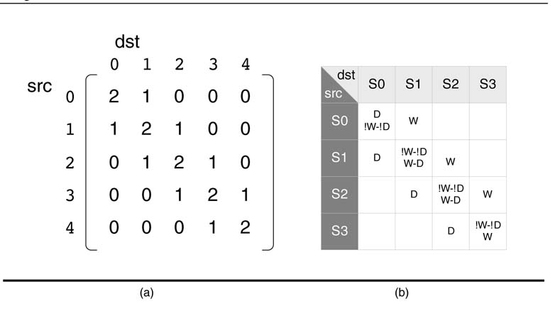
Example:Write an adjacency matrix for the ASM of the 4-entry FIFO of Section 9.4.2 that traverses all possible paths from the matrix for automatic test vector generation.
Solution: All the paths start from the first node S0 and terminate on other nodes in the FSM; the nodes are as shown in Figure 9.19. There are two paths that start and endatS0. Corresponding to each path, a sequence of inputs is generated. For example, fora direct path originating from S0 and ending at S3, the following sequence of inputs generates the path:
Similarly, the same path ending at S3 with error output is:
9.7 Methods for Reducing Power Dissipation
9.7.1 Switching Power
The distribution network of the clock and clock switching are the two major sources of power consumption. The switching power is given by the expression:
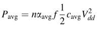
where n is the total number of nodes in the circuit, eave is the average switching activity on a node, f is the clock frequency, and DVD is the power supply voltage. Obviously, killing the clock on the distribution network and reducing the average switching activity can reduce the average power dissipation.
In a design with complex state machines, the state machine part is the major user of power. This power consumption can be reduced by clock gating techniques.
9.7.2 Clock Gating Technique
FSM-based designs in general wait for an external event to change states. These designs, even if there is no event, still continuously check the input and keep transitioning into the same state at every clock cycle. This dissipates power unnecessarily. By careful analysis of the state machine specification, the designer can turn the power off if the FSM is in a self-loop. This requires stopping the clock by gating it with output from self-loop detection logic. This is shown in Figure 9.20. The latch L in the design is used to block glitches in the output generated by gated logic fig [20]. The function fig implements logic to detect whether the machine is in self-loop. The logic can be tailored to cater for only highly probable self-loop cases. This does require an a priori knowledge of the transition statistics of the implemented FSM.
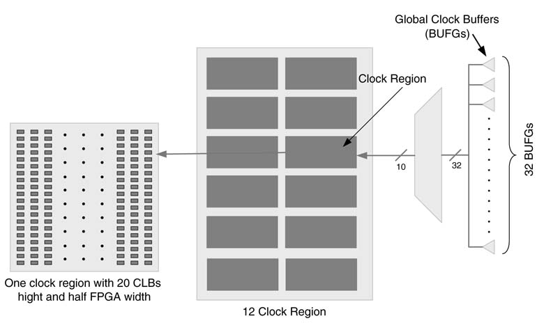
Clock gating techniques are well known to ASIC designers [17–19], and now even for FPGAs effective clock gating techniques have been developed. FPGAs have dedicated clock networks to take the clock to all logic blocks with low skew and low jitter.
To illustrate the technique on a modern FPGA, the example of the Exiling Virtex-5 FPGA is considered in [24]. An FPGA in this family has several embedded blocks such as block RAM, DSP48 and Ions, but for hardware configuration the basic building blocks of the FPGA are the configurable logic blocks (Clubs). Each CLB consists of two slices, and each slice contains four 6-input look-up tables (Lust) and four flip-flops. The FPGA has 32 global clock buffers (Budges) to support these many internal or externally generated clocks. The FPGA is divided into multiple clock regions. Out of these 32 global clock signals, any 10 signals can be selected to be simultaneously fed to a clock region. Figure 9.21 shows a Virtex-5 device with 12 clock regions and associated logic of selecting 10 clocks out of 32 for these regions.
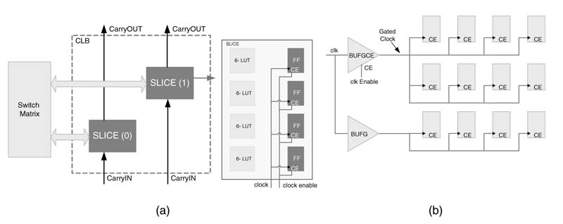
All the flip-flops in a slice also come with a clock enabling signal, as shown in Figure 9.22(a). Although disabling this signal will save some power, the dynamic power dissipated in the clock distribution network will remain. To save this power, each clock buffer BUFGCE also comes with an enabling signal, as shown in Figure 9.22(b). This signal can also be disabled internally to kill the clock being fed to the clock distribution network. The methodology for using the clock enabling signal of flip-flops in a slice for clock gating is given in [24].
Figure 9.20 Low-power FSM design with gated clock logic
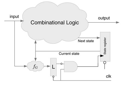
Figure 9.21 Virtex-5 with32 global cock buffers with10clock regions and several Closing each region
9.7.3 FSM Decomposition
FSM decomposition is a technique where by an FSM is optimally partitioned into multiple sub-FSMs in such a way that the state machine remains OFF in most of the sub-FSMs for a considerable time.
Figure 9.22 ClockgatinginVirtex-5 FPGA. (a) CLB with two slices and a slicewith four LUTs and four FFs with clock enable signal. (b) Gating the clocks to FFs
In the best-case scenario this leads to only clocking one of the sub-FSMs in any given cycle. Disabling of the clock trees for all other sub-FSMs by gating the clock signal can greatly reduce power consumption [25].
The example here illustrates the grouping of an FSM into sub-FSMs using a graph partitioning method. The technique uses the probability of transition of states to pack a set of nodes that are related with each other into individual sub-FSMs. Consider an FSM be divided into Mpartitions of sub-FSMs with each having number of states S0,S1,...,SM-1. Then, for easy coding, the number of bits allocated for a state register for each of the sub-FSMs is:
and log2M bits is required for switching across sub-FSMs.
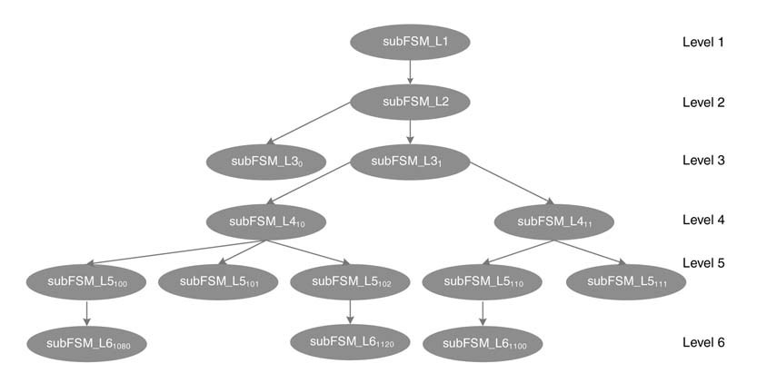
Many algorithms translating into complex FSMs are hierarchical in nature. This property can be utilized in optimally partitioning the FSM into sub-FSMs for power reduction. The algorithm is broken in to different levels, with each level leading to a different sub-FSM. The hierarchical approach ensures that, when the transition is made from higher level to lower level, the other sub-FSMs will not be triggered for the current frame or buffer of data. This greatly help sinreducing power consumption.
A video decoder is a good application to be mapped on hierarchical FSMs. The design for an H.264 decoder otherwise needs 186 states in aflattened FSM. The whole FSM is active and generates huge switching activity. By adopting hierarchical parsing of decoder frames and then traversing the FSM, the design can be decomposed into six levels with 13 sub-FSMs [25]. The designer, knowing the state transition patterns, can also assign state code that has minimum hamming distance among closely transitioned states to reduce switching activities.
Many algorithms in signal processing can be hierarchically decomposed. A representative decomposition is given in Figure 9.23. Each sub-FSM should preferably have a single point of entry to make it convenient to design and test. Each sub-FSM should also be self-contained to maximize transitions within the sub-FSM and to minimize transitions across sub-FSMs. The design is also best for power gating for power optimization.
Figure 9.23 An FSM hierarchically partitioned into sub-FSMs for effective design, implementation, testing and power optimization
Exercises
Exercise 9.1
Design a 4 × 4-bit-serial unsigned multiplier that assumes bit-serial inputs and output [26]. Modify the multiplier to perform Q1.3 fractional signed × signed multiplication. Truncate the result to 4-bit Q1.3 format by ignoring least significant bits of the product.
Exercise 9.2
Using the fractional bit-serial multiplier of exercise 9.1, design a bit-serial 3-coefficient FIR filter. Assume both the coefficients and data are in Q1.3 format. Ignore least significant bits to keep the output in Q1.3 format.
Exercise 9.3
Design a sequential architecture for an IIR filter implementing the following difference equation:
First Write the sequential pseudo-code for the implementation, then design a single MAC-based architecture with associated logic. Assume the circuit clock is 21 times the sampling clock. All the coefficients are in Q1.15 format. Also truncate the output to fit in Q1.15 format.
Exercise 9.4
Design the sequential architectures of 4-coefficient FIR filters that use: (a) one sequential multiplier; and (b) four sequential multipliers.
Exercise 9.5
Design an FSM that detects an input sequence of 1101. Implement the FSM using Mealy and Moore techniques, and identify whether Moore machine implementation takes more states. For encoding the states use a one-hot technique. Write RTLVerilog code of the design. Write test vectors to test all the possible transitions in the state machine.
Exercise 9.6
Design a smart traffic controller for the roads layout given in Figure 9.24. The signals on Main Road should cater for all the following:
1.The traffic on the minor roads, VIP and ambulance movements on the main roads (assume a sensing system is in place that informs about VIP, ambulance movements, and traffic on the minor roads). The system, when it turns the Main Road light to red, automatically switches lights on the minor roads to green.
2.The system keeps all traffic lights on Main Road green if it detects the movement of a VIP or an ambulance on the main road, while keeping the minor road lights red. The lights remain in this state for an additional two minutes after the departure of the designated vehicles from Main Road.
3.If sensors on minor roads 1, 2 or 3 sense traffic, the lights for the traffic on Main Road are turned red for 80 seconds.
4.If the sensor on any one of the minor roads senses traffic, the light for Main Road traffic on that crossing is turned red for 40 seconds, and on the rest of the crossing for 20 seconds.
5.If the sensors on any two of the minor roads senses traffic, the lights on those crossings are turned red for 50 seconds while light on the left over third crossing is turned red for 30 seconds.
6.Once switched from red to green, the lights on Main Road remains green at least for the next 200 seconds.
Figure 9.24 Road layout for exercise 9.6
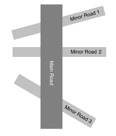
Draw a bubble diagram of the state machine, clearly marking input and outputs, and Write RTL Verilog code of the design. Design a comprehensive test-bench that covers all transitions of the FSM.
Exercise 9.7
Design a state machine that outputs 1 at every fifth 1 input as a Mealy and Moore machine. Check your design for the following bit stream of input:
Exercise 9.8
Design a Moore machine system to detect three transitions from0to 1 or1to0.Describe your design using an ASM chart. Assume a serial interface where bits are serially received at every positive edge of the clock. Implement the design in RTL Verilog. Write a stimulus to check all transitions in the FSM.
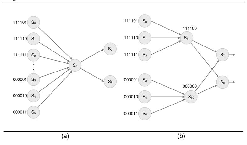
Figure 9.25 FSM from bench-marking database of exercise 9.9
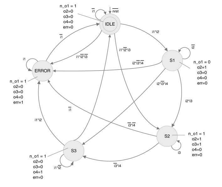
Exercise 9.9
The state machine of Figure 9.25 is represented using a bubble diagram. The FSM is taken from a database that is used for bench-marking different testing and performance issues relating to FSMs.
1. Describe the state machine using a mathematical model. List the complete setofinputsX,states S and output Y.
2. Write the adjacency matrix for the state machine.
3. Write RTL Verilog code of the design that adheres to RTL coding guidelines for FSM design.
4. Write test vectors that traverse all the arcs at least once.
5. Exercise 9.10
Design an FSM-based 4-deep LIFO to implement the following:
1. A Write into the LIFO Writes data on INBUS at the end of the queue.
2. A DELETE from LIFO DELETEs the last entry in the queue.
3. A Write and DELETE at the same time generates an error.
4. A Write in a full queue and a DELETE from an empty queue also generates an error.
5. The last entry to the queue is always available at the OUTBUS.
Draw the datapath and ASM diagram and Write RTLVerilog code of the design. Write the adjacency matrix and develop a stimulus that generates a complete set of test vectors that traverse all paths of the FSM.
Exercise 9.11
Design the datapath and an ASM chart for implementing the controller of a queue that consists of four registers, R0, R1, R2 and R3.
1. The operations on the queue are INSERT_Ri to register Ri and DELETE_Ri from register Ri, for i = 0... 3.
2. INSERT_Ri moves data from the INBUS to the Ri register, readjusting the rest of the registers. For example, if the head of the queue is R2, INSERT_R1 will move data from the INBUS in R1 and move R1 to R2., and R2 to R3, keeping R0 as it is and the head of the queue to R3.
3. DELETE_Ri DELETE the value in the Ri register, and readjusts the rest of the registers. For example, DELETE_R1 will move R2 to R1 and R3 to R2, keeping R0 as it is and move the head of the queue to R2 from R3.
4. The head of the queue is always available on the OUTBUS.
5. INSERTion into a full queue or deletion from an empty queue causes an error condition.
6. Assertion of INSERT and DELETE at the same time causes an error condition
Exercise 9.12
Designa3-entry FIFO, which supports Write, DEL0, DEL1 and DEL2, where Write Writes to the tail of the queue, and DEL0, DEL1 andDEL2 delete last, last two or all three entries from the queue, respectively. When insufficient entries are in the queue for a DELi operation, the FIFO controller generates an error, ERRORd. Similarly, Write in a completely filled FIFO also generates an error, ERRORw.
1. Design the datapath.
2. Design the state machine-based controller of the FIFO. Design the FSM implementing the controller and describe the design using an ASM diagram.
3. Write RTL Verilog code of the design.
4. Develop a stimulus that traverses all the states.
Exercise 9.13
Design a time-shared FIR filter that implements a 12-coefficient FIR filter using two MAC units. Clearly show all the registers and associated clocks. Use one CPA in the design. Write RTL code for the design and test the design for correctness.
Exercise 9.14
Develop a state machine-based instruction dispatcher that reads 64-bit words from the instruction memory into two 64-bit registers IR0 and IR1. The least significant two bits of the instruction depicts
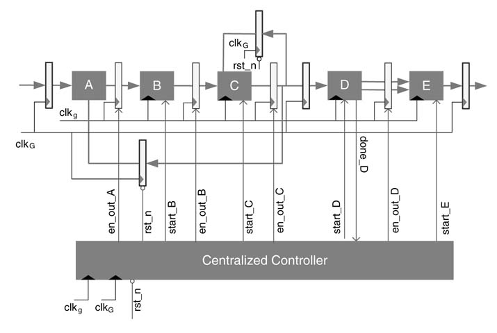
Figure 9.26 Centralized controller for exercise 9.15
whether the instruction is 16-bit, 32-bit, 48-bit or 64-bit wide. Use the two instruction registers such that IR1 always keep a complete valid instruction.
Exercise 9.15
Write RTL Verilog code for the design given in Figure 9.26. Node A is a combinational logic, and nodes B, C and E take 7, 8 and 9 predefined number of circuit clocks, clkg. Node D dynamically executes and takes a variable number of cycles between 3and 8.7. Assume simple counters inside the nodes. Write a top-level module with two input clocks,clkg and clog. All control signals are 1-bit and the data width is 8 bits. For each block A, B, C, D and E, only Write module instances. Design a controller for generating all the control signals in the design.
References
B. A. Curtis and V. K. Madisetti, “A quantitative methodology for rapid prototyping and high-level synthesis of signal processing algorithms,” IEEE Transactions on Signal Processing, 1994, vol. 42, pp. 3188–3208.
G. A. Constantinides, P. Cheung and W. Luk, “Optimum and heuristic synthesis of multiple word-length architectures,” IEEE Transactions on VLSI Systems, 2005, vol. 13, pp. 39–57.
P. T. Balsara and D. T. Harper “Understanding VLSI bit-serial multipliers,” IEEE.TransactionsonEducation, 1996, vol. 39, pp. 19–28.
S. A. Khan and A. Perwaiz, “Bit-serial CORDIC DDFS design for serial digital dowN-converter,” in Proceedingsof Australasian Telecommunication Networks and Applications Conference, 2007, pp. 298–302.
S. Matsuo et al. “8.9-megapixel video image sensor with 14-b columN-parallel SA-ADC,” IEEETransactionsonElectronic Devices, 2009, vol. 56, pp. 2380–2389.
R. Hartley and P. Corbett, “Digit-serial processing techniques,” IEEETransactionsonCircuitsandSystems, 1990, vol. 37, pp. 707–719.
K. K. Parhi, “A systematic approach for design of digit-serial signal processing architectures,” IEEETransactionson Circuits and Systems, 1991, vol. 38, pp. 358–375.
T. Sansaloni, J. Valls and K. K. Parhi, “Digit-serial complex-number multipliers on FPGAs,” JournalofVLSI Signal Processing Systems Archive, 2003, vol. 33, pp. 105–111.
N.Nedjah and L. d. M. Mourelle, “Three hardware architectures for the binary modular exponentiation: sequential, parallel and systolic,” IEEE Transactions on Circuits and Systems I, 2006, vol. 53, pp. 627–633.
M. Keating and P. Bricaud. Reuse Methodology Manual for System-oN-a-Chip Designs, 2002, Kluwer Academic.
P. Zimmer, B. Zimmer and M. Zimmer, “FizZim: an opeN-source FSM design environment,” design paper, Zimmer Design Services, 2008.
G. De Micheli, R. K. Brayton and A. Sangiovanni-Vincentelli, “Optimal state assignment for finite state machines,” IEEE Transactions on Computer-Aided Design of Integrated Circuits and Systems, 1985, vol. 4, pp. 269–285.
W. Wolf, “Performance-driven synthesis in controller-datapath systems,” IEEE Transactions on Very Large Scale Integration Systems, 1994, vol. 2, pp. 68–80.
Transeda: www.transeda.com
Verisity: www.verisity.com/products/surecov.xhtml
Asic-world: www.asic-world.com/verilog/tools.xhtml
Q. Wang and S. Roy, “Power minimization by clock root gating,” Proceedings of DAC, IEEE/ACM, 2003, pp. 249–254.
M. Donno, A. Ivaldi, L. Benini and E. Macii, “Clock tree power optimization based on RTL clock-gating,” Proceedings of DAC, IEEE/ACM, 2003, pp. 622–627.
H.Mahmoodi,V.Tirumalashetty,M.Cooke andK.Roy, “Ultra-low-power clocking scheme using energy recovery and clock gating,” IEEE Transactions on Very Large Scale Integration Systems, 2009, vol. 17, pp. 33–44.
L. Benini, P. Siegel and G. De Micheli, “Saving power by synthesizing gated clocks for sequential circuits,” IEEEDesign and Test of Computers, 1994, vol. 11, pp. 32–41.
Q. Wang and S. Roy, “Power minimization by clock root gating,” Proceedings of DAC, IEEE/ACM, 2003, pp. 249–254.
M. Donno, A. Ivaldi, L. Benini and E. Macii, “Clocktree power optimization based on RTL clock-gating,” Proceedings of DAC, IEEE/ACM, 2003, pp. 622–627.
V. K. Madisetti and B. A. Curtis, “A quantitative methodology for rapid prototyping and high-level synthesis of signal processing algorithms,” IEEE Transactions on Signal Processing, 1994, vol. 42, pp. 3188–3208.
Q. Wang, S. Gupta and J. H. Anderson, “Clock power reduction for Virtex-5 FPGAs,” in Proceedingsof International Symposium on Field Programmable Gate Arrays, ACM/SIGDA, 2009, pp. 13–22.
K. Xu, O. Chiu-sing Choy, C.-F. Chan and K.-P. Pun, “Power-efficient VLSI realization of a complex FSM for H.264/AVC bitstream parsing,” IEEE Transactions on Circuits and Systems II, 2007, vol. 54, pp. 984–988.
R. Gnanasekaran, “On a bit-serial input and bit-serial output multiplier,” IEEETransactionsonComputers, 1983, vol. 32, pp. 878–880.
The Benefits of SystemVerilog for ASIC Design and Verification, Ver 2.5 Synopsys jan 2007 (http://www.synopsys.com/Tools/Implementation/RTLSynthesis/CapsuleModule/sv_asic_wp.pdf)