
2
Using a Hardware Description Language
2.1 Overview
This chapter gives a comprehensive coverage of Verilog and SystemVerilog. The focus is mostly on Verilog, which is a hardware description language (HDL).
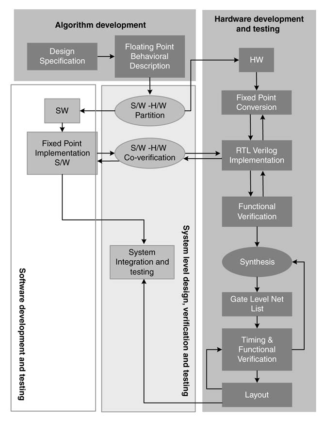
The chapter starts with a discussion of a typical design cycle in implementing a signal processing application. The cycle starts with the requirements specification, followed by the design of an algorithm using tools like MATLAB®. To facilitate partitioning of the algorithm into hardware (HW) and software (SW), and its subsequent mapping on different platforms, algorithm design and coding techniques in MATLAB® are described. The MATLAB® code has to be structured so that the algorithm developers, SW designers and HW engineers can correlate various components and can seamlessly integrate, test and verify the design and can return to the original MATLAB® implementation if there are any discrepencies in the results.
The chapter then has a brief account of Verilog. As there are several textbooks available on Verilog [1-3], this chapter focuses primarily on design and coding guidelines and relevant rules. There is a particular emphasis on coding rules for keeping synthesis in perspective. A description of ‘register transfer level’ (RTL) Verilog is presented. RTL signifies the placement of registers in hardware while keeping an account of the movement of data among these registers.
SystemVerilog adds more features for modeling and verification. Although Verilog itself provides constructs to write test benches for verification, it lacks features that are required to verify a complex design. Traditionally verification engineers have resorted to other languages, such as Vera or e, or have used a ‘program language interface’ (PLI) to interface Verilog code with verification code written in C/C ++. The use of PLI requires complex interface coding. SystemVerilog enhances some of the features of Verilog for hardware design, but more importantly adds powerful features that facilitate verification of more complex designs. Assertion, interface, package, coverage and randomization are examples of some of these features.
2.2 About Verilog
2.2.1 History
Philip Moorby invented Verilog in1983/84. At that time he was with Gateway Design Automation. VHDL is another language used for designing hardware. It was with the advent of synthesis tools by Synopsys in1987 when Verilog and VHDL started to change the whole paradigm and spectrum of hardware design methodology. Within a few years, HDLs became the languages of choice for hardware design.In 1995, Open Verilog International (OVI) IEEE-1364 placed Verilogin the public domain to compete with VHDL [4].
It was critical for Verilog to keep pace with the high densities predicted by Moore’s Law. Now the average process geometries are shrinking and billion-transistor chips are designed using 45-nm and smaller nanometer technologies.
The Verilog standard is still evolving. More and more features and syntax are being added that, on one hand, are providing higher level of abstraction, and on the other hand are helping the test designer to effectively verify an RTL design. Most of this advancement has been steered by the IEEE. Following the release of IEEE standard 1364-1995,in1997 the IEEE formed another working group to add enhancements to the existing Verilog standard. The new standard was completed in 2001, and this variant of the language is called Verilog-2001 [5]. It provides additional support, flexibility and ease of programming to developers.
In 2001, a consortium (Accellara) of digital design companies and electronic design automation (EDA) tool vendors set up a committee to work on the next generation of extensions to Verilog. In 2003, the consortium released SystemVerilog 3.0, without ratification. In 2004, it released System-Verilog 3.1 [6] which augmented in Verilog-2001 many features that facilitated design and verification. In 2005, while still maintaining two sets of standards, the IEEE released Verilog-2005 [7] and SystemVerilog-2005 [8], the latter adding more features for modeling and verification.
2.2.2 What is Verilog?
Verilog is a hardware description language. Although it looks much like C, it is not a software programming language. It is very important for the Verilog programmer to understand hardware concepts. Each line of Verilog code in the design means one or more components in hardware.
Verilog is rich in constructs and functionality. Some of the constructs are specific to supporting verification and modeling and do not synthesize to infer hardware. The synthesis is performed using a synthesis tool , which is a compiler that translates Verilog into a gate-level design. The synthesis tool understands only a subset of Verilog, the part of Verilog called ‘RTL Verilog’. All the other constructs are ‘non-RTL Verilog’. These constructs are very helpful in testing, verification and simulation.
It is imperative for the designer to know at the register transfer level what is being coded in the design. The RTL signifies the placement of registers in the design and the flow of data among the registers. The complete Verilog is a combination of RTL and non-RTL constructs. A good hardware designer must have sound understanding of these differences and comprehensive command of RTL Verilog constructs. The programmer must also have a comprehension of the design to be coded in RTLVerilog.
Advancements in technology are allowing designers to realize ever more complex designs, posing real challenges for testing and verification engineers. The testing of a complex design requires creativity and ingenuity. Many features specific to verification are being added in SystemVerilog, which is a companion standard supported by most of the Verilog tool vendors. Verilog also provides a socket-level interface, known as ‘programming language interface’ (PLI), to be used with other programming environments such as C/C ++,.NET, JavE and MATLAB®. This has extended the scope of hardware design verification from HW designers to SWengineers. Verification has become a challenging and exciting discipline. The author’s personal experience in designing application-specific ICs with many million gates to complex systems on FPGAs has convinced him that the verification of many designs is even more challenging then designing the system itself. While designing, the designer needs to use genuine creativity and special abilities to make interesting explorations in the design space. The author believes that hardware design is an art, though techniques presented in this book provide excellent help; but coding a design in RTL is a well-defined and disciplined science. This chapter discusses Verilog coding with special focus on RTL and verification.
2.3 System Design Flow
Figure 2.1 shows a typical design flow of a design implementing a signal processing application. An explanation of this flow is given in Chapter 3. This section only highlights that a signal processing application is usually divided into software and hardware components. The hardware design is implemented in Verilog. The design is then mapped either on custom ASICs or FPGAs. This design needs to work with the rest of the software application. There are usually standard interfaces that enable the SW and HW components to transfer data and messages.
Architecture is designed to implement the hardware part of the application. The design contains all the requisite interfaces for communicating with the part implemented in software. The SW is mapped on a general-purpose processor (GPP) or digital signal processor (DSP). The HW design and the interfaces are coded in Verilog. This chapter focuses on RTL coding of the design and its verification for correct functionality. The verified design is synthesized on a target technology. The designer, while synthesizing the design, also constrains the synthesis tool either for timing or area. The tool generates a gate-level netlist of the design. The tool also reports if there are paths that are not meeting the timing constraints defined by the designer for running the HW at the desired clock speed. If that happens, the designer either makes the tool meet the timing by trying different synthesis options, or transforms the design by techniques described in this book. The modified design is re-coded in RTL and the process of synthesis is repeated until the design meets the defined timings. The gate-level netlist is then sent for a physical layout, and for custom ASICs the design is then ‘taped-out’ for fabrication. The field-programmable gate array tools provide an integrated environment for synthesis, layout and implementation of a bit stream to FPGA.
2.4 Logic Synthesis
The code written in RTL Verilog is synthesized for gate-level implementation. The synthesis process takes the RTL Verilog and translates it into an optimized gate-level netlist. For logic synthesis the user specifies design constraints and the target technology in the form of a standard cell library. The library has standard basic logic gates such as AND and OR, or macro cells like adders, multipliers, flip-flops, multiplexers and so on. The tool completely converts the design described in RTL hardware description language into a design that contains standard cells.
To optimally map the high-level description into real HW, the tool performs several steps. A typical flow of synthesis first converts the RTL description into non-optimized Boolean logic. It then performs several transformations to optimize the logic subject to user constraints. This optimization is independent of the target technology. Finally, the tool maps the optimized logic to technology-specific standard cells.
Figure 2.1 System-level design components
2.5 Using the Verilog HDL
2.5.1 Modules
AVerilog code has a top-level module, which may instantiate many other modules. The module is the basic building block in Verilog. Each module contains statements and instantiation of lower level modules.InRTL design this module, once synthesized, infers digital logic. The designer conceives a hardware design as hierarchically interconnecting lower level modules forming higher level modules. In the next level of hierarchy, the modules so constructed are further connected to design even high level modules. Thus the design has multiple layers of modules. At the top level the designer may also conceive the functionality of an application in terms of interconnected modules. Individual modules may also be incrementally synthesized to facilitate synthesis of large designs.
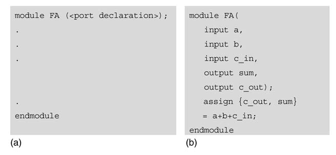
Figure 2.2 Module definition (a) template (b) example
Modules are declared and instantiated like classes in C++, but module declarations cannot be nested. Instances of low-level modules are interconnected, and modules have ports for these interconnections.
Figure 2.2(a) shows a template of a module definition. A module starts with keyword module and ends with keyword endmodule . The ports of a module can be input, output or in_out . Figure 2.2(b) shows a simple example to illustrate the concept: the module FA has three input ports, a, b and c_in, and two output ports, sum and c_out .
2.5.2 Design Partitioning
2.5.2.1 Guidelines for RTL Design
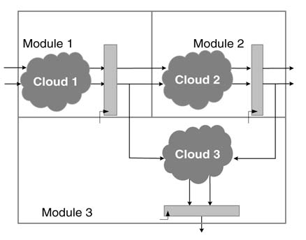
A guide for effective RTL coding from the synthesis perspective is given in Figure 2.3 [9]. The partitioning of a digital design into a number of modules is important. A module should be neither too small nor too large. Where possible, the design should be partitioned in a way that module boundaries reside at register outputs, as shown in the figure. This will make it easier to synthesize the top-level module or hierarchical synthesis at any level with timing constraints. The designer should also ensure that no combination cloud crosses module boundaries. This gives the synthesis tool more leverage to generate optimized logic.
Figure 2.3 Design partitioning in number of modules with module boundaries on register outputs
2.5.2.2 Guidelines for System Level Design Flow
The design flow of a digital design process has been shown in Figure 2.1. A system designer first captures requirements and specifications (R&S) of the real-time system under design. Implementation of the algorithm in SW or HW needs to perform computations on the input data and produce output data at the specified rates. For example, for a multimedia processing system, the requirement can be in terms of processing P color or grayscale frames of N × M pixels per second. The processing may be compression, rendering, object recognition and so on. Similarly for digital communication applications, the requirement can be described in terms of data rates and the communication standard that modulates this data for transmission. An example is a design that supports up to a 54-Mbps OFDM-based communication system that uses a 64-QAM modulation scheme.
Algorithm development is one of the most critical steps in system design. Algorithms are developed using tools such as MATLAB®, Simulink or C/C ++ /C#, or in any high-level language. Functionally meeting R&S is a major consideration when the designer selects an algorithm out of several options. For example, in pattern matching the designer makes an intelligent choice out of many techniques including ‘chamfer distance transform’, ‘artificial neural network’ and ‘correlation-based matching’.
Although meeting functional requirements is the major consideration, the developer must keep in mind the ultimate implementation of the algorithm on an embedded platform consisting of ASICs, FPGAs and DSPs. To ease design partitioning on a hybrid embedded platform, it is important for a system designer to define all the components of the design, clearly specifying the data flow among them. A component should implement a complete entity with defined functionality in the design. It is quite pertinent for the system designer to clearly define inputs and outputs and internal variables.
The program flow should be defined as it will happen in the actual system. For example, with hard real-time signal processing systems, the data is processed on a block by block basis. In this form, a buffer of input data is acquired and is passed to the first component in the system. The component processes this buffer of data and passes the output to the component next in execution order. Alternatively, in many applications, especially in communication receiver design, the processing is done on a sample by sample basis. In these types of application the algorithmic implementation should process data sample by sample. Adhering to these guidelines will ease the task of HW/SW partitioning, co-design and co-verification.
The design is sequentially mapped from high-level behavioral design to embedded system partitioning in HW mapped on ASICs or FPGAs and SW running on embedded DSPs or microcontrollers. It is important for the designers in the subsequent phases in the design cycle to stick to the same components and variable names as far as possible. This greatly facilitates going back and forth in the design cycle while the designer is making refinements and verifying its functionality and performance.
2.5.3 Hierarchical Design
Verilog works well with a hierarchical modeling concept. Verilog code contains a top-level module and zero or more instantiated modules. The top-level module is not instantiated anywhere. Several instantiations of a lower-level module may exist. Verilog is an HDL and, unlike with other programming languages, once synthesized each instantiation infers a physical copy of the HW with its own logic gates, registers and wires. Ports are used to interconnect instantiated modules.
Figure 2.4 Verilog FA module with input and output ports. (a) Port declaration in module definition and port listing follows the definition (b) Verilog-2001 support of ANSI style port listing in module definition
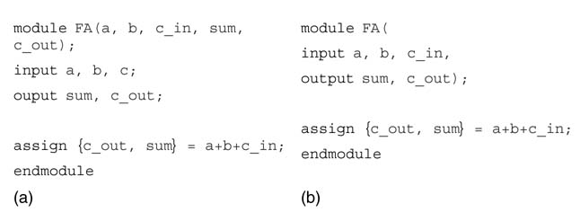
Figure 2.4 shows two ways of listing ports in a Verilog module. In Verilog-95, ports are defined in the module definition and then they are listed in any order. Verilog-2001 also supports ANSI-style port listing, whereby the listing is incorporated in the module definition.
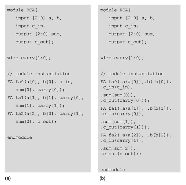
Using the FA module of Figure 2.4(a), a 3-bit ripple carry adder (RCA) can be designed. Figure 2.5 shows the composition of the adder as three serially connected FAs. To realize this simple design in Verilog, the module RCA instantiates FA three times. The Verilog code of the design is given in Figure 2.6(a).
If ports are declared in Verilog-95 style, then the order of port declaration in the module definition is important but the order in which these ports are listed as input, output, c_in and c_out on the following lines has no significance. As Verilog-2001 lists the ports in the module boundary, their order should be maintained while instantiating this module in another module.
For modules having a large number of ports, this method of instantiation is error-prone and should be avoided . The ports of the instantiated module then should be connected by specifying names. In this style of Verilog, the ports can be connected in any order, as demonstrated in Figure 2.6(b).
Figure 2.5 Design of a 3-bit RCA using instantiation of three FAs
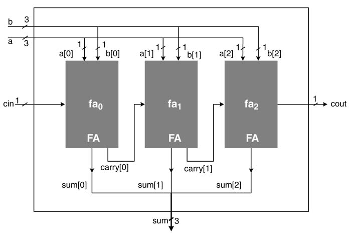
Figure 2.6 Verilog module for a 3-bit RCA. (a) Port connections following the order of ports definition in the FA module. (b) Port connections using names
2.5.3.1 Synthesis Guideline: Avoid Glue Logic
While the designer is hierarchically partitioning the design in a number of modules, the designer should avoid glue logic that connects two modules [9]. This may happen after correcting an interface mismatch or adding some missing functionality while debugging the design. Glue logic is demonstrated in Figure 2.7. Any such logic should be made part of the combinational logic of one of the constituent modules. Glue logic may cause issues in synthesis as the individual modules may satisfy timing constraints whereas the top-level module may not. It also prevents the synthesis tool from generating a fully optimized logic.
2.5.3.2 Synthesis Guideline: Design Modules with Common Design Objectives
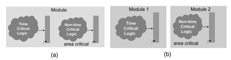
The designer must avoid placing time-critical and non-time-critical logic in the same module [9],as in Figure 2.8(a). The module with time-critical logic should be synthesized for best timing, whereas the module with non-time-critical logic is optimized for best area. Putting them in the same module will produce a sub-optimal design. The logic should be divided and placed into two separate modules, as depicted in Figure 2.8(b).
Figure 2.7 Glue logic at the top level should be avoided
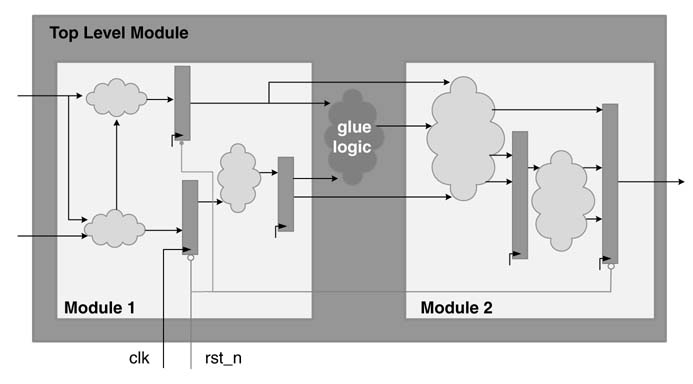
Figure 2.8 Synthesis guidelines. (a) A bad design in which time-critical and non-critical logics are placed in the same module. (b) Critical logic and non-critical logic placed in separate modules
2.5.4 Logic Values
Unlike with other programming languages, a bit in Verilog may contain one of four values, as given in Table 2.1. It is important to remember that there is no unknown value in a real circuit, and an ‘x’ in simulation signifies only that the Verilog simulator cannot determine a definite value of 0 or 1.
Table 2.1 Possible values a bit may take in Verilog
| 0 | Zero, logic low, false,or ground |
| 1 | One, logic high,or power |
| x | Unknown |
| z | High impedance, unconnected, or tri-state port |
While running a simulationinVerilog the designer may encounter a variable taking a combination of the above values at different bit locations. In binary representation, the following is an example of a number containing all four possible values:
20' b 0011_1010_101x_x0z0_011z
The underscore character (_) is ignored by Verilog simulators and synthesis tools and is used simply to give better visualization to a long string of binary numbers.
2.5.5 Data Types
Primarily there are two data types in Verilog, nets and registers.
2.5.5.1 Nets
Nets are physical connections between components. The net data types are wire, tri, wor, trior, wand, triand, tri0, tri1, supply0, supply1 and trireg .An RTLVerilog code mostly uses the wire data type. A variable of type wire represents one or multiple bit values. Although this variable can be used multiple times on the right-hand side in different assignment statements,it can be assigned a value in an expression only once. This variable is usually an output of a combinational logic whereas it always shows the logic value of the driving components. Once synthesized, a variable of type wire infers a physical wire.
2.5.5.2 Registers
A register type variable is denoted by reg . Register variables are used for implicit storage as values should be written on these variables, and unless a variable is modified it retains its previously assigned value. It is important to note that a variable of type reg does not necessarily imply a hardware register; it may infer a physical wire once synthesized. Other register data types are integer, time and real .
AVerilog simulator assigns ‘x’ as the default value to all uninitialized variables of type reg . If one observes a variable taking a value of ‘x’ in simulation, it usually traces back to an uninitialized variable of type reg.
2.5.6 Variable Declaration
In almost all software programming languages, only variables with fixed sizes can be declared. For example, in C/C + + a variable can be of type char, short or int . Unlike these languages, a Verilog variable can take any width. The variable can be signed or unsigned. The following syntax is used for declaring a signed wire:
wire signed [<range>] <net_name> <net_name>*;
Here*implies optional and the range is specified as[Most Significant bit (MSb): Least Significant bit (LSb)]. It is read as MSb down to LSb. If not specified, the default value of the range is taken as one bit width. A similar syntax is used for declaring a signed variable of type reg :
reg signed [<range>] <reg_name> <reg_name>*;
A memory is declared as a two-dimensional variable of type reg, the range specifies the width of the memory, and start and end addresses define its depth. The following is the syntax for memory declaration in Verilog:
reg [<range>] <memory_name> [<start_addr>: <end_addr>];
The Verilog code in the following example declares two 1-bit wide signed variables of type reg (x1 and x2) , two 1-bit unsigned variables of type wire (y1 and y2), an 8-bit variable of type reg (temp), and an 8-bit wide and 1-Kbyte deep memory ram-local . Note that a double forward slanted bar is used in Verilog for comments:
reg signed x1, x2; // 1-bit signed variables of type reg x1 and x2
wire y1, y2; // 1-bit variables of type wire, y1 and y2
reg [7:0] temp; // 8-bit reg temp
reg [7:0] ram_local [0:1023]; //8-bit wide and 1-Kbyte deep memory
A variable of type reg can also be initialized at declaration as shown here:
reg x1 = 1’b0; // 1-bit reg variable x1 initialize to 0 at declaration
2.5.7 Constants
Like variables, a constant in Verilog can be of any size and it can be written in decimal, binary, octal or hexadecimal format. Decimal is the default format. As the constant can be of any size, its size is usually written with ‘d’, ‘b’, ‘o’ or ‘h’ to specify decimal, binary, octal or hexadecimal, respectively. For example, the number 13 can be written in different formats as shown in Table 2.2.
2.6 Four Levels of Abstraction
As noted earlier, Verilog is a hardware description language. The HW can be described at several levels of detail. To capture this detail, Verilog provides the designer with the following four levels of abstraction:
- switch level
- gate level
- dataflow level
- behavioral or algorithmic level.
A design in Verilog can be coded in a mix of levels, moving from the lowest abstraction of switch level to the highly abstract model of behavioral level. The practice is to use higher levels of abstraction like dataflow and behavioral while designing logic in Verilog. A synthesis tool then translates the design coded using higher levels of abstraction to gate-level details.
Table 2.2 Formats to represent constants
| Decimal | 13 or 4d13 |
| Binary | 4'b1101 |
| Octal | 4'o15 |
| Hexadecimal | 4'hd |
2.6.1 Switch Level
The lowest level of abstraction is switch- or transistor-level modeling. This level is used to construct gates, though its use is becoming rare as CAD tools provide a better way of designing and modeling gates at the transistor level. A digital design in Verilog is coded at RTL and switch-level modeling is not used in RTL, so this level is not covered in this chapter. Interested readers can get relevant information on this topic from the IEEE standard document on Verilog [7].
2.6.2 Gate Level or Structural Modeling
Gate-level modeling is at a low level of abstraction and not used for coding design at RTL. Our interest in this level arises from the fact that the synthesis tools compile high-level code and generate code at gate level. This code can then be simulated using the stimulus earlier developed for the RTL-level code. The simulation at gate level is very slow compared with the original RTL-level code. A selective run of the code for a few test cases may be performed to derive confidence in the synthesized code. The synthesis tools have matured over the years and so are the coding guidelines. Gate-level simulation is also becoming rare.
Gate-level simulation can be performed with timing information in a standard delay file (SDF). The SDF is generated for pre-layout or post-layout simulation by, respectively, synthesis or place and route tools. The designer can run simulation using the gate-level netlist and the SDF. There is a separate timing calculator in all synthesis tools. The calculator provides timing violations if there are any. For synchronous designs the use of gate-level simulation for post-synthesis or layout timing verification is usually not required.
The code at gate level is built from Verilog primitives . These primitives are built-in gate-level models of basic functions, including nand, nor, and, or, xor, buf and not . Modeling at this level requires describing the circuit using logic gates. This description looks much like an implementation of a circuit in a basic logic design course. Delays can also be modeled at this level. A typical gate instantiation is
and #delay instance-name (out, in1, in2, in3)
The first port in the primitive, out , is always a 1-bit output followed by several 1-bit inputs (here in1, in2 and in3 ); the and is a Verilog primitive that models functionality of an AND gate, while #delay specifies the delay from input to output of this gate.
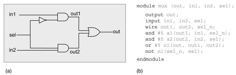
Example 2.1
This example designs a 2:1 multiplexer at gate level using Verilog primitives. The design is given in Figure 2.9(a). The sel wire selects one of the two inputs in1 and in2 . sel = 0 in1 is selected, otherwise in2 is selected. The implementation requires and, not and or gates, which are available as Verilog primitives. Figure 2.9(b) lists the Verilog code for the gate-level implementation of the design. Note #5, which models delay from input to output of the AND gate. This delay in Verilog is a unit-less constant. It gives good visualization once the waveforms of input and output are plotted in a Verilog simulator. These delays are ignored by synthesis tools.
Figure 2.9 (a) A gate-level design for a 2 : 1 multiplexer. (b) Gate-level implementation of a 2 : 1multiplexer using Verilog primitives
2.6.3 Dataflow Level
This level of abstraction is higher than the gate level. Expressions, operands and operators characterize this level. Most of the operators used in dataflow modeling are common to software programmers, but there are a few others that are specific to HW design. Operators that are used in expressions for dataflow modeling are given in Table 2.3. At this level every expression starts with the keyword assign. Here is a simple example where two variables a and b are added to produce c:
assign c = a + b;
The value on wire c is continuously driven by the result of the arithmetic operation. This assignment statement is also called ‘continuous assignment’. In this statement the right-hand side must be a variable of type wire , whereas the operands on the left-hand side may be of type wire or reg.
Table 2.3 Operators for dataflow modeling
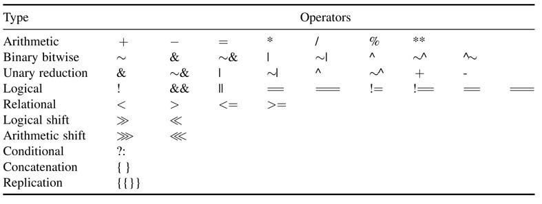
Table 2.4 Arithmetic operators
| Operator type | Operator symbol | Operation performed |
| Arithmetic | * | Multiply |
| / | Divide | |
| + | Add | |
| - | Subtract | |
| % | Modulus | |
| ** | Power |
2.6.3.1 Arithmetic Operators
The arithmetic operators are given in Table 2.4. It is important to understand the significance of using these operators in RTL Verilog code as each results in a hardware block that performs the operation specified by the operator. The designer should also understand the type of HW the synthesis tool generates once the code containing these operators is synthesized. In many circumstances, the programmer can specify the HW block from an already developed library to synthesis tools. Many FPGAs have build-in arithmetic units. For example, the Xilinx family of devices have embedded blocks for multipliers and adders. While writing RTL Verilog for targeting a particular device, these blocks can be instantiated in the design. The following code shows instantiation of two built-in 18 × 18 multipliers in the Virtex-II family of FPGAs:
// Xilinx 18x18 built-in multipliers are instantiated MULT18X18 m1(out1, in1, in2); MULT18X18 m2(out2, in3, in4);
The library from Xilinx also provides a model for MULT18x18 for simulation. Adders and multipliers are extensively used in signal processing, and use of a divider is preferably avoided. Verilog supports both signed and unsigned operations. For signed operation the respective operands are declared as signed wire or reg .
The size of the output depends on the size of the input operands and the type of operation. The multiplication operator results in an output equal to the sum of sizes of both the operands. For addition and subtraction the size of the output is the size of the wider operand and a carry or borrow bit.
2.6.3.2 Conditional Operators
The conditional operator of Table 2.5 infers a multiplexer. A statement with the conditional operator is:
out = sel ? a: b;
Table 2.5 Conditional operator
| Operator type | Operator symbol | Operation performed |
| Conditional | ?: | Conditional |
This statement is equivalent to the following decision logic:
if(sel)
 out = a;
else
 out = b;
The conditional operator can also be used to infer higher order multiplexers. The code here infers a 4:1 multiplexer:
out = sel[1] ? (sel[0] ? in3: in2): (sel[0] ? in1: in0);
2.6.3.3 Concatenation and Replication Operators
Most of the operators in Verilog are the same as in other programming languages, but Verilog provides a few that are specific to HW designs. Examples are concatenation and replication operators, which are shown in Table 2.6.
Example 2.2
Using a concatenation operator, signals or parts of signals can be concatenated to make a new signal. This is a very convenient and useful operator for the hardware designer, who can bring wires from different parts of the design and tag them with a more appropriate name. In the example in Figure 2.10, signals a[3:0], b[2:0], 3’b111 and c[2:0] are concatenated together in the specified order to make a 13-bit signal,
Table 2.6 Concatenation and replication operators
| Operator type | Operator symbol | Operation performed |
| Concatenation | {} | Concatenation |
| Replication | {{}} | Replication |
Figure 2.10 Example of a concatenation operator
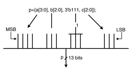
Table 2.7 Logical operators
| Operator type | Operator symbol | Operation performed |
| Logical | ! | Logical negation |
| || | Logical OR | |
| && | Logical AND |
Example 2.3
A replication operator simply replicates a signal multiple times. To illustrate the use of this, let
A = 2’b01;
B = {4{A}} // the replication operator
The operator replicates A four times and assigns the replicated value to B.
Thus B= 8'b 01010101.
2.6.3.4 Logical Operators
These operators are common to all programming languages (Table 2.7). They operate on logical operands and result in a logical TRUE or FALSE. The logical negation operator (!) checks whether the operand is FALSE, then it results in logical TRUE; and vice versa. Similarly, if one or both of the operands is TRUE, the logical OR operator (||) results in TRUE; and FALSE otherwise. The logical AND operator is TRUE if both the logical operands are TRUE, and it is FALSE otherwise. When one of the operands is an x, then the result of the logical operator is also x.
The bitwise negation operator (~) is sometimes mistakenly used as a logical negation operator. In the case of a multi-bit operand, this may result in an incorrect answer.
2.6.3.5 Logic and Arithmetic Shift Operators
Shift operators are listed in Table 2.8. Verilog can perform logical and arithmetic shift operations. The logical shift is performed on reg and wire .
Example 2.4
Right shifting of a signal by a constant n drops n least significant bits of the number and appends the n most significant bits with zeros. For example, shift an unsigned reg A= 6'b101111 by 2:
B = A >> 2;
Table 2.8 Shift operators
| Operator type | Operator symbol | Operation performed |
| Logic shift | ≫ | Unsigned right shift |
| ≪ | Unsigned left shift | |
| Arithmetic shift | ⋙ | Signed right shift |
| ⋘ | Signed left shift |
This drops two LSBs and appends two zeros at the MSB position, thus:
B = 60b001011
Example 2.5
Arithmetic shift right of an operand by n drops the n LSBs of the operand and fills the n MSBs with the sign bit of the operand. For example, shift right a wire A = 6 ’ b101111 by 2:
B = A >>> 2;
This operation will drop two LSBs and appends the sign bit to two MSB locations. Thus B= 6’b111011.
Arithmetic and logic shift left by n performs the same operation, as both drop n MSBs of the operand without any consideration of the sign bit.
2.6.3.6 Relational Operators
Relational operators are also very common to software programmers and are used to compare two numbers (Table 2.9). These operators operate on two operands as shown below:
result = operand1 OP operand2;
This statement results in a logical value of TRUE or FALSE. If one of the bits of any of the operands is an x, then the operation results in x.
2.6.3.7 Reduction Operators
Reduction operators are also specific to HW design (Table 2.10). The operator performs the prescribed operation on all the bits of the operand and generates a 1-bit output.
Table 2.9 Relational operator
| Relational operator | Operator symbol | Operation performed |
| > | Greater than | |
| < | Less than | |
| >= | Greater than or equal to | |
| <= | Less than or equal to |
Table 2.10 Reduction operators
| Operator type | Operator symbol | Operation performed |
| Reduction | & | Reduction AND |
| ~& | Reduction NAND | |
| | | Reduction OR | |
| ~| | Reduction NOR | |
| ^ | Reduction XOR | |
| ^~ or ~^ | Reduction XNOR |
Example 2.6
Apply the & reduction operator to a 4-bit number A = 4 ’ b1011:
assign out = &A;
This operation is equivalent to performing a bitwise & operation on all the bits of A:
out = A[0] & A[1] & A[2] & A[3];
2.6.3.8 Bitwise Arithmetic Operators
Bitwise arithmetic operators are also common to software programmers. These operators perform bitwise operations on all the corresponding bits of the two operands. Table 2.11 gives all the bitwise operators in Verilog.
Example 2.7
This example performs bitwise | operation on two 4-bit numbers A = 4 ’ b1011 and B = 4 ’ b0011 . The Verilog expression computes a 4-bit C :
assign C = A | B;
performs the OR operation on corresponding bits of A and B and the operation is equivalent to:
C[0] = A[0] | B[0]
C[1] = A[1] | B[1]
C[2] = A[2] | B[2]
C[3] = A[3] | B[3]
2.6.3.9 Equality Operators
Equality operators are common to software programmers, but Verilog offers two flavors that are specific to HW design: case equality (= = =) and case inequality (!= =). A simple equality operator (= =) checks whether all the bits of the two operands are the same.If any operand has an x or z as one of its bits, the answer to the equality will be x. The = = =operator is different from = = as it also matchesx withx andz withz . The result of this operator is always a 0 or a 1 . There is a similar difference between != and != =. The following example differentiates the two operators.
Table 2.11 Bitwise arithmetic operators
| Operator type | Operator symbol | Operation performed |
| Bitwise | ~ | Bitwise negation |
| & | Bitwise AND | |
| ~& | Bitwise NAND | |
| | | Bitwise OR | |
| ~| | Bitwise NOR | |
| ^ | Bitwise XOR | |
| ^~or~^ | Bitwise XNOR |
Table 2.12 Equality operators
| Operator type | Operator symbol | Operation performed |
| Equality | = = | Equality |
| != | Inequality | |
| = = = | Case equality | |
| != = | Case Inequality |
Example 2.8
While comparing A = 4 ’ b101x and B = 4 ’ b101x using = = and = = = , out = (A = = B)will be x and out = (A = = = B) will be 1 (Table 2.12).
2.6.4 Behavioral Level
The behavioral level is the highest level of abstraction in Verilog. This level provides high-level language constructs like for, while, repeat, if-else and case . Designers with a software programming background already know these constructs.
Although the constructs are handy and very powerful, the programmer must know that each construct in RTL Verilog infers hardware. High-level constructs are very tempting to use, but the HW consequence of their inclusion must be well understood. For example, for loop to a software programmer suggests a construct that simply repeats a block of code a number of times, but if used in RTL Verilog the code infers multiple copies of the logic in the loop. There are behavioral-level synthesis tools that take a complete behavioral model and synthesize it, but the logic generated using these tools is usually not optimal. The tools are not used in those designs where area, power and speed are important considerations.
Verilog restricts all the behavioral statements to be enclosed in a procedural block . In a procedural block all variables on the left-hand side of the statements must be declared as of type reg, whereas operands on the right-hand side in expressions may be of type reg or wire.
There are two types of procedural block, always and initial .
2.6.4.1 Always and Initial Procedural Blocks
A procedural block contains one or multiple statements per block.An assignment statement used in a procedural block is called a procedural assignment. The initial block executes only once, starting at t =0 simulation time, whereas an always block executes continuously at t = 0 and repeatedly thereafter.
The characteristics of an initial block are as follows.
- This block starts with the initial keyword.Ifmultiple statements are used in the block, they are enclosed within begin and end constructs, as shown in Figure 2.11.
- This block is non-synthesizable and non-RTL. This block is used only in a stimulus.
- There are usually more than one initial blocks in the stimulus. All initial blocks execute concurrently in arbitrary order, starting at simulation time 0.
- The simulator kernel executes the initial block until the execution comes to a #delay operator. Then the execution is suspended and the simulator kernel places the execution of this block in the event list for delay-time units in the future.
- After completing delay-time units, the execution is resumed where it was left off.
Figure 2.11 Initial and always blocks
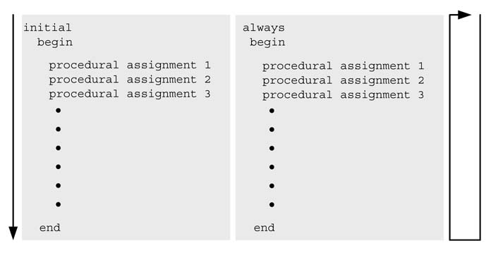
An always block is synthesizable provided it adheres to coding guidelines for synthesis. From the perspective of its execution in a simulator, an always block behaves like an initial block except that, once it ends, it starts repeating itself.
2.6.4.2 Blocking and Non-blocking Procedural Assignments
All assignments in a procedural block are called procedural assignments. These assignments are of two types, blocking and non-blocking. A blocking assignment is a regular assignment inside a procedural block. These assignments are called blocking because each assignment blocks the execution of the subsequent assignments in the sequence. In RTL Verilog code, these assignments are used to model combinational logic. For the RTL code to infer combinational logic, the blocking procedural assignments are placed in an always procedural block.
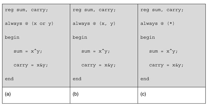
There are several ways of writing what is called the sensitivity list in an always block. The sensitivity list helps the simulator in effective management of simulation. It executes an always block only if one of the variables in the sensitivity list changes. The classical method of sensitivity listing is to write all the inputs in the block in a bracket, where each input is separated by an ‘or’ tag. Verilog-2001 supports comma-separated sensitivity lists. It also supports just writing a ‘*’ for the sensitivity list. The simulator computes the list by analyzing the block by itself.
The code in Figure 2.12 illustrates the use of a procedural block to infer combinational logic in RTL Verilog code. The always block contains two blocking procedural assignments. The sensitivity list includes the two inputs x and y, which are used in the procedural block. A list of inputs x and y to these assignments are placed with the always statement. This list is the sensitivity list. This procedural block once synthesized will infer combinational logic. The three methods of writing a sensitivity list are shown in Figure 2.12.
It should also be noted that, as the left-hand side of a procedural assignment must be of type reg, so sum and carry are defined as variables of type reg.
In contrast to blocking procedural assignments, non-blocking procedural assignments do not block other statements in the block and these statements execute in parallel. The simulator executes this functionality by assigning the output of these statements to temporary variables, and at the end of execution of the block these temporary variables are assigned to actual variables.
Figure 2.12 Blocking procedural assignment with three methods of writing the sensitivity list. (a) Verilog-95 style. (b) Verilog-2001 support of comma-separated sensitivity list. (c) Verilog-2001 style that only writes * in the list
The left-hand side of the non-blocking assignment must be of type reg. The non-blocking procedural assignments are primarily used to infer synchronous logic. Shown below is the use of a non-blocking procedural assignment that infers two registers, sum_reg and carry_reg :
reg sum_reg, carry_reg;
always @ (posedge clk)
begin
 sumreg ⇐x^y;
 carry_reg ⇐x&y;
end
Both of the non-blocking assignments are simultaneously executed by the simulator. The use of a blocking assignment in generating synchronous logic is further explained in the next section.
2.6.4.3 Multiple Procedural Assignments
From the simulation perspective, all procedural blocks simultaneously start execution at t =0. The simulator, however, schedules their execution in an arbitrary order. Now a variable of data type reg can be assigned values at multiple locations in a module. Any such multiple assignments to a variable of type reg must always be placed in the same procedural block. If a variable is assigned values in different procedural blocks and the values are assigned on it at the same time, the value assigned to the variable depends on the order in which the simulator executes these blocks. This may cause errors in simulation and pre- and post-synthesis results may not match.
2.6.4.4 Time Control # and @
Verilog provides different timing constructs for modeling timing and delays in the design. The Verilog simulator works on unit-less timing for simulating logic. The simulated time at any instance in the design can be accessed using built-invariable $time .It is a unit-less integer. The timing at any instance in simulation can be displayed by using the $display as shown here:
$display ($time, “a=%d”, a);
The programmer can insert delays in the code by placing #<number>. On encountering this statement, the simulation halts the execution of the statement until <number> of time units have passed. The control is released from that statement or block so that other processes can execute. Synthesis tools ignore this statement in RTLVerilog code, and the statements are mostly used in test code or to model propagation delay in combinational logic.
Another important timing control directive in Verilog is @. This directive models event-based control. It halts the execution of the statement until the event happens. This timing control construct is used to model combinational logic as shown here:
always @ (a or b)
 c = a^b;
Here the execution of the assignment statement always @(a or b) will happen only if a or b changes value. These signals are listed in the sensitivity list of the block.
The time control @ is used also to model synchronous logic. The code here models a positive-edge trigger flip-flop:
always @(posedge clk)
 dout <= din;
It is important to note that, while coding at RTL, the non-blocking procedural assignment should be used only to model synchronous logic and the blocking procedural assignment to model combinational logic.
2.6.4.5 RTL Coding Guideline: Avoid Combinational Feedback
The designer must avoid any combinational feedback in RTL coding. Figure 2.13(a) demonstrates combinational feedback, as does the following code:
reg [15:0] acc;
always@(acc)
 acc = acc + 1;
Figure 2.13 Combinational feedback must be voided in RTL Verilog code. (a) A logic with combinational feedback. (b) The register is placed in the feedback path of a combinational logic
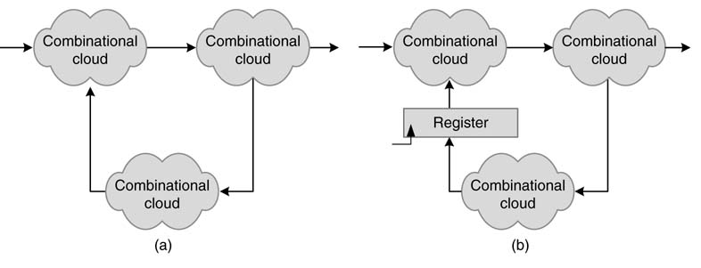
Any such code does not make sense in design and simulation. The simulator will never come out of this block as the change in acc will bring it back into the procedural block. If logic demands any such functionality,a register should be used to break the combinational logic,as shown in Figure 2.13(b) where a register is placed in the combinational feedback paths.
2.6.4.6 The Feedback Register
In many digital designs, a number of registers reside in feedback paths of combinational logic. Figure 2.14 shows digital logic of an accumulator with a feedback register. In designs with feedback registers there must be a reset, because a pre-stored value in a feedback register will corrupt all future computations. From the simulation perspective, Verilog assumes a logic value x in all register variables. If this value is not cleared, this x feeds back to a combinational cloud in the first cycle and may produce a logic value x at the output. Then, in all subsequent clock cycles the simulator – irrespective of the input data to the combinational cloud – may compute x and keep showing x at the output of the simulation. A register can be initialized using a synchronous or an asynchronous reset. In both cases, an active-low or active-high reset signal can be used. An asynchronous active-low reset is usually used in designs because it is available in most technology libraries. Below are examples of Verilog code to infer registers with asynchronous active-low and active-high resets for the accumulator example;
// Register with asynchronous active-low reset
always @ (posedge clk or negedge rst_n) begin
 if(!rst_n)
 acc_reg <= 16’b0;
 else
 acc_reg <= data+acc_reg;
 end
// Register with asynchronous active-high reset
always @ (posedge clk or posedge rst)
begin
 if(rst)
 acc_reg <= 16’b0;
 else
 acc_reg <= data+acc_reg;
 end
Figure 2.14 Accumulator logic with a feedback register
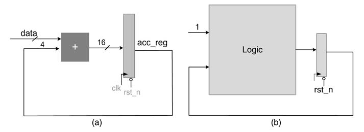
The negedge rst_n and posedge rst directives in the always statement and subsequently if(! rst_n) and if (rst) statements in each block, respectively, are used to infer these resets. To infer registers with synchronous reset, either active-low or active-high, the always statement in each block contains only the posedge clk directive. Given below are examples of Verilog code to infer registers with synchronous active-low and active-high resets:
// Register with asynchronous active-low reset
always @ (posedge clk)
begin
 if(!rst_n)
 acc_reg <=16’b0;
 else acc_reg <= data+acc_reg;
end
// Register with asynchronous active-high reset
always @ (posedge clk)
begin
 if(rst)
 acc_reg <=16’b0;
 else
 acc_reg <= data+acc_reg;
end
2.6.4.7 Generating Clock and Reset
The clock and reset that go to every flip-flop in the design are not generated inside the design. The clock usually comes from a crystal oscillator outside the chip or FPGA. In the place and route phase of the design cycle, clocks are specially treated and are routed using clock trees. These are specially designed routes that take the clocks to registers and flip-flops while causing minimum skews to these special signals. In FPGAs, the external clocks must be tied to one of the dedicated pins that can drive large nets. This is achieved by locking the clock signal with one of these pins. For Xilinx it is done in a ‘user constraint file’ (UCF). This file lists user constraints for placement, mapping, timing and bit generation [11].
Similarly, the reset usually comes from outside the design and is tied to a pin that is physically connected with a push button used to reset all the registers in the design.
To test and verify RTL Verilog code, clock and reset signals are generated in a stimulus. The following is Verilog code to generate the clock signal clk and an active-low reset signal rst_n:
initial // All the initializations should be in the initial block
begin
 clk =0; // clock signal must be initialized to 0
 #5 rst_n = 0; // pull active low reset signal to low
 #2 rst_n=1; // pull the signal back to high
end
always // generate clock in an always block
 #10 clk=(~clk);
These blocks are incorporated in the stimulus module. From the stimulus these signals are input to the top-level module.
2.6.4.8 Case Statement
Like C and other high-level programming languages, Verilog supports switch and case statements for multi-way decision support. This statement compares a value with number of possible outcomes and then branches to its match.
The syntax inVerilog is different from the format used in C/C++ The following code shows the use of the case statement to infer a 4:1 multiplexer:
module mux4_1(in1, in2, in3, in4, sel, out);
input [1:0] sel;
input [15:0] in1, in2, in3, in3;
output [15:0] out;
reg [15:0] out;
always @(*)
begin
 case (sel)
 2’b00: out = in1;
 2’b01: out = in2;
 2’b10: out = in3;
 2’b11: out = in4;
 default: out = 16’bx;
 endcase
end
endmodule
The select signal sel is evaluated, and the control branches to the statement that matches with this value. When the sel value does not match with any listed value, the default statement is executed. Two variants of case statements, case z and case x , are used to make comparison with the ‘don’t care’ situation. The statement casez takes z as don’t care, whereas case x takes z and x as don’t care. These don’t care bits can be used to match with any value. This provision is very handy while implementing logic where only a few of the bits are used to take a branch decision:
always @(op_code)
begin
casez (op_code)
 4’b1???: alu_inst(op_code);
 4’b01??: mem_rd(op_code);
 4’b001?: mem_wr(op_code);
 endcase
end
This block compares only the bits that are specified and switches to one of the appropriate tasks. For example, if the MSB of the op_code is 1, the casez statement selects the first statement and the alu_inst task is called.
2.6.4.9 Conditional Statements
Verilog supports the use of conditional statements in behavioral modeling. The if-else statement evaluates the expression. If the expression is TRUE it branches to execute the statements in the if block, otherwise the expression may be FALSE, 0, x or z , so the statements in else block are executed. The example below gives a simple use. If the brach_flag is non-zero, the PC is equated to brach_addr ; otherwise if the brach_flag is 0 , x or z , the PC is assigned the value of next_addr .
if (brach_flag)
 PC = brach_addr
else
 PC = next_addr;
The if-(else if)-else conditional statement provides multi-way decision support. The expressions in if-(else if)-else statements are successively evaluated and, if any of the expressions is TRUE, the statements in that block are executed and the control exits from the conditional block. The code below demonstrates the working of multi-way branching using the if-(else if)-else statement:
always @(op_code)
 begin
 if (op_code == 2’b00)
 cntr_sgn = 4’b1011;
 else if (op_code == 2’b01;
 cntr_sgn = 4’b1110;
else
 cntr_sgn = 4’b0000;
end
The code successively evaluates the op_code in the order specified in if, else if and else statements and, depending on the value of op_code , it appropriately assigns value to cntr_sgn .
2.6.4.10 RTL Coding Guideline: Avoid Latches in the Design
A designer must avoid any RTL syntax that infers latches in the synthesized net list. A latch is a storage device that stores a value without the use of a clock. Latches are usually technology-specific and must be avoided in synchronous designs. To avoid latches the programmer must adhere to coding guidelines.
For decision statements, the programmer should either fully specify assignments or must use a default assignment. A variable in an if statement in a procedural block for combinational logic infers a latch if it is not assigned a value under all conditions. This is depicted in the following code:
input [1:0] sel;
reg [1:0] out_a, out_b;
always @ (*)
 begin
 if (sel == 2’b00)
 begin
 out_a = 2’b01;
 out_b = 2’b10;
end
else
 out_a = 2’b01;
end
As out_b is not assigned any value under else, the synthesis tool will infer a latch for storing the previous value of out_b in cases where an else condition is TRUE. To avoid this latch the programmer should either assign some value to out_b in the else block, or assign default values to all variables outside a conditional block. This is shown in the following code:
input [1:0] sel;
reg [1:0] out_a, out_b;
always @(*)
 begin
 out_a = 2’b00;
 out_b = 2’b00;
 if (sel=2’b00)
 begin
 out_a = 2’b01;
 out_b = 2’b10;
 end
 else
 out_a = 2’b01;
end
The syntheses tool will also infer a latch when conditional code in the combinational block misses any one or more conditions. This scenario is depicted in the following code:.
input [1:0] sel;
reg [1:0] out_a, out_b;
always @*
 begin
 out_a = 2’b00;
 out_b = 2’b00;
 if (sel==2’b00)
 begin
 out_a = 2’b01;
 out_b = 2’b10;
end
else if (sel == 2’b01)
 out_a = 2’b01;
end
This code misses some possible values of sel and checks for only two listed values, 2’b01 and 2’b00 . The synthesis tool will infer a latch for out_a and out_b to retain previous values in case any one of the conditions not covered occurs. This s type of coding must be avoided. In an if, else if, else block, the block must come with an else statement; and in scenarios where the case statement is used, either all conditions must be specified, and for each condition values should be assigned to all variables, or a default condition must be used and all variables must be assigned default values outside the conditional block. The correct way of coding is depicted here:
always @*
 begin
 out_a = 2’b00;
 out_b = 2’b00;
 if (sel==2’b00)
 begin
 out_a = 2’b01;
 out_b = 2’b10;
 end
 else if (sel == 2’b01)
 out_a = 2’b01;
 else
 out_a = 2’b00;
end
Here is the code showing the correct use of case statements:
always @*
 begin
 out_a = 2’b00;
 out_b = 2’b00;
 case (sel)
 2’b00:
 begin
 out_a = 2’b01;
 out_b = 2’b10;
 end
 2’b01:
 out_a = 2’b01;
 default:
 out_a = 2’b00;
 endcase
end
2.6.4.11 Loop Statements
Loop statements are used to execute a block of statements multiple times. Four types of loop statement are supported in Verilog: forever, repeat, while and for. The statement forever continuously executes its block of statements. The remaining three statements are commonly used to execute a block of statements a fixed number of times . Their equivalence is shown below. For repeat:
i=0;
repeat (5)
begin
 $display("i=%d
", i);
 i=i+1;
end
For while:
i=0;
while (i<5)
begin
 $display("i=%d
", i);
 i=i+1;
end
For for:
for (i=0; i<5; i=i+1)
 begin
 $display("i=%d
", i);
end
2.6.4.12 Ports and Data Types
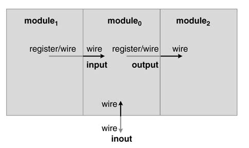
In Verilog, input ports of a module are always of type wire . An output, if assigned in a procedural block,is declared as reg , and in cases where the assignment to the output is made using a continuous assignment statement, then the output is defined as a wire . The in out is always defined as a wire . The data types are shown in Figure 2.15.
The input to a module is usually the output of another module, so the figure shows that the output of module1 is the input to module0. The port declaration rules can be easily followed using the arrow analogy, whereby the head of the arrow drawn across the module must be defined as wire and the tail declared as reg or wire depending on whether the assignment is made inside a procedural block or in a continuous assignment.
2.6.4.13 Simulation Control
Verilog provides several system tasks that do not infer any hardware and are used for simulation control. All system tasks start with the sign $. Some of the most frequently used tasks and the actions they perform are listed here.
Figure 2.15 Port listing rules in Verilog. Head is always a wire. Tail may be a wire or reg based on whether it is, respectively, an assignment statement or a statement in a procedure block
- $finish makes the simulator exit simulation.
- $stop suspends the simulation and the simulator enters an interactive mode, but the simulation can be resume from the point of suspension.
- $display prints an output using a format similar to C and creates a new line for further printing.
- $monitor is similar to $display but it is active all the time. Only one monitor task can be active at any time in the entire simulation. This task prints at the end of the current simulation time the entire list when one of the listed values changes.
The following example gives the format of $monitor and $display which closely resemble the printf() function in C:
$monitor($time, “A=%d, B=%d, CIN=%b, SUM=%d, COUT=%d”, A, B, CIN, SUM, COUT);
$display($time, “A=%d, B=%d, CIN=%b, SUM=%d, COUT=%d”, A, B, CIN, SUM, COUT);
$time in these statements prints the simulation time at the time of execution of the statement. These statements display the values of A, B, CIN and COUT in decimal, binary, decimal and decimal number representations, respectively. The directives %d, %o, %h and %b are used to print values in decimal, octal, hexadecimal and binary formats, respectively.
$fmonitor and $fdisplay write values in a file. The file first needs to be open using $fopen . The code below shows the use of these tasks for printing values in a file:
modulator_vl = $fopen("modulator.dat");
if (modulator_vl == 0) $finish;
$fmonitor(modulator_vl,"data=%h bits=%h", data_values, decision_bits);
2.6.4.14 Loading Memory Data from a File
System tasks $readmemb and $readmemh are used to load data from a text file written in binary or hexadecimal, respectively, into specified memory. The example here illustrates the use of these tasks. First memory needs to be defined as:
reg [7:0] mem[0:63];
The following statement loads data in a memory.dat file into mem:
$readmemb (“memory.dat”, mem);
2.6.4.15 Macros
Verilog supports several compiler directives. These directives are similar to C programming precompiler directives. Like #define inC, Verilog provides ‘define to assign a constant value toatag:
‘define DIFFERENCE 6’b011001
The tag can then be used instead of a constant in the code. This gives better readability to the code. The use of the ‘define tag is shown here:
if (ctrl == ‘DIFFERENCE)
2.6.4.16 Preprocessing Commands
These are conditional pre-compiler directives used to selectively execute a piece of code:
‘ifdefG723
$display (“G723 execution”);
‘else
$display (“other codec execution”);
‘endif
The ‘include directive works like #include in C and copies the contents in the file at the location of the statement. The statement
‘include “filename.v”
copies the contents of filename.v at the location of the statement.
2.6.4.17 Comments
Verilog supports C-type comments. Their use is shown below:
reg a; // One-line comment
Verilog also supports block comments (as in C):
/* Multi-line comment that
reg acc;
results in the reg acc declaration being commented out */
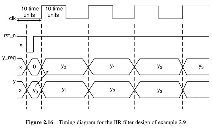
Example 2.9
This example implements a simple single-tap infinite impulse response (IIR) filter in RTL Verilog and writes its stimulus to demonstrate coding of a design with feedback registers. The design implements the following equation:
y[n] = 0.5y[n—1] +x[n]
The multiplication by 0.5 is implemented by an arithmetic shift right by 1 operation. A register y_reg realizes y[n — 1] in the feedback path of the design, thus needing reset logic. The reset logic is implemented as an active-low asynchronous reset. The module has 16-bit data x, clock clk , reset rst_n as inputs and the value of y as output. The module IIR has two procedural blocks. One block models combinational logic and the other sequential. The block that models combinational logic consists of an adder and hard-wired shifter. The adder adds the input data x in shifted value of y_reg . The output of the combinational cloud is assigned to y. The sequential block latches the value of y in y_re g . The RTL Verilog code for the module IIR is given below:
module iir(
input signed [15:0] x,
input clk, rst_n,
output reg signed [31:0] y);
reg signed [31:0] y_reg;
always @(*) \ combinational logic block
y =(y_reg>>>1) + x;
 always @(posedge clk or negedge rst_n) \ sequential logic block
begin
 if (!rst_n)
 y_reg <= 0;
 else
 y_reg <= y;
 end
 endmodule
The stimulus generates a clock and a reset signal. This reset is applied to the feedback register before the first positive edge of the clock. Initialization on clock and generation of reset is done in an initial block. Another initial block is used to give a set of input values to the module. These values are generated in a loop. The monitor statement prints the input and output with simulation time on the screen. The $stop halts the simulation after 60 time units and $finish ends the simulation. It is important to note that a simulation with clock input must be terminated using $finish, otherwise it never ends. The code for the stimulus is listed below:
module stimulus_irr;
reg [15:0] X;
reg CLK, RST_N;
wire [31:0] Y;
integer i;
iir IRR0(X, CLK, RST_N, Y); \ instantiation of the module
initial
 begin
 CLK = 0;
 #5 RST_N = 0; \ resetting register before first posedge clk
 #2 RST_N = 1;
end
initial
 begin
X = 0;
 for(i=0; i<10; i=i+1) \ generating input values every clk cycle
 #20 X = X + 1;
$finish;
end
always \ clk generation
 #10 CLK = CLK;
initial
$monitor($time, " X=%d, sum=%d, Y=%d", X, IRR0.y, Y);
 initial
begin
 #60 $stop;
 end
endmodule
Figure 2.16 Timing diagram for the IIR filter design of example 2.9
2.6.4.18 Timing Diagram
In many instances before writing Verilog code and stimuli, it is quite useful to sketch a timing diagram. This is usually a great help in understanding the interrelationships of different logic blocks in the design. Figure 2.16 illustrates the timing diagram for the IIR filter design of the pervious subsection.
A clock is generated with time period of 20 units. The active-low reset is pulled low after 5 time units and then pulled high after 2 time units. As soon as the reset is pulled low, the y_reg is cleared and set to 0. The first posedge of the clock after 10 time units latches the output of the combinational logic y into y_reg . The timing diagram should be drawn first and then accordingly coded in stimulus and checked in simulation for validity of results.
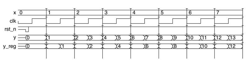
All Verilog simulators also provide waveform viewers that can show the timing diagram of selected variables in the simulation run. Figure 2.17 shows the screen output of the waveform viewer of ModelSim simulator for the IIR filter example above.
2.6.4.19 Parameters
Parameters are constants that are local to a module. A parameter is assigned a default value in the module and for every instance of this module it can be assigned a different value.
Figure 2.17 Timing diagram from the ModelSim simulator
Parameters are very handy in enhancing the reusability of the developed modules. A module is called parametered if it is written in a way that the same module can be instantiated for different widths of input and output ports. It is always desirable to write parameterized code, though in many instances it may unnecessarily complicate the coding.
The following example illustrates the usefulness of a parameterized module:
module adder (a, b, c_in, sum, c_out);
parameter SIZE = 4;
 input [SIZE-1: 0] a, b;
 output [SIZE-1: 0] sum;
 input c_in;
 output c_out;
assign {c_out, sum} = a + b + c_in;
endmodule
The same module declaration using ANSI-style port listing is given here:
module adder
 #(parameter SIZE = 4)
 (input [SIZE-1: 0] a, b,
 output [SIZE-1: 0] sum,
 input c_in,
 output c_out);
This module now can be instantiated for different values of SIZE by merely specifying the value while instantiating the module. Shown below is a section of the code related to the instantiation of the module for adding 8-bit inputs, in1 and in2 :
module stimulus;
 reg [7:0] in1, in2;
wire [7:0] sum_byte;
 reg c_in;
wire c_out;
adder #8 add_byte (in1, in2, c_in, sum_byte, c_out);
.
.
endmodule
In Verilog, the parameter value can also be specified by name, as shown here:
adder #(.SIZE(8)) add_byte (in1, in2, c_in, sum_byte, c_out);
Multiple parameters can also be defined in a similar fashion. For example, for the module that adds two unequal width numbers, the parameterized code is written as:
module adder
#(parameter SIZE1 = 4, SIZE2=6)
 (input [SIZE1-1: 0] a,
 input [SIZE2-1: 0] b,
 output [SIZE2-1: 0] sum,
 input c_in,
 output c_out);
The parameter values can then be specified using one of the following two options:
adder #(.SIZE1(8),.SIZE2(10)) add_byte
 (in1, in2, c_in, sum_byte, c_out);
or, keeping the parameters in the same order as defined:
adder #(8,10) add_byte (in1, in2, c_in, sum_byte, c_out);
2.6.5 Verilog Tasks
Verilog task can be used to code functionality that is repeated multiple times in a module. A task has input, output and inout and can have its local variables. All the variables defined in the module are also accessible in the task. The task must be defined in the same module using task and endtask keywords.
To use a task in other modules, the task should be written in a separate file and the file then should be included using an ‘include directive in these modules. The tasks are called from initial or always blocks or from other tasks in a module. The task can contain any behavioral statements including timing control statements. Like module instantiation, the order of input, output and inout declarations in a task determines the order in which they must be mentioned for calling. As tasks are called in a procedural block, the output must be of type reg , whereas the inputs may be of type reg or wire . Verilog-2001 adds a keyword automati c to the task to define are-entrant task.
The following example designs a task FA and calls it in a loop four times to generate a 4-bit ripple carry adder:
module RCA(
 input [3:0] a, b,
 input c_in,
 output reg c_out,
 output reg [3:0] sum
);
reg carry[4:0];
integer i;
task FA(
 input in1, in2, carry_in,
 output reg out, carry_out);
 {carry_out, out} = in1 + in2 + carry_in;
endtask
 always@*
begin
 carry[0]=c_in;
 for(i=0; i<4; i=i+1)
 begin
 FA(a[i], b[i], carry[i], sum[i], carry[i+1]);
 end
 c_out = carry[4];
end
endmodule
2.6.6 Verilog Functions
Verilog function is in many respects like task as it also implements code that can be called several times inside a module. A function is defined in the module using function and endfunction keywords. The function can compute only one output. To compute this output, the function must have at least one input. The output must be assigned to an implicit variable bearing the name and range of the function. The range of the output is also specified with the function declaration. A function in Verilog cannot use timing constructs like # or @. A function can be called from a procedural block or continuous assignment statement. It may also be called from other functions and tasks, whereas a function cannot call a task. A re-entrant function can be designed by adding the automatic keyword.
A simple example here writes a function to implement a 2:1 multiplexer and then uses it three times to design a 4:1 multiplexer:
module MUX4to1(
 input [3:0] in,
 input [1:0] sel,
 output out);
 wire out1, out2;
 function MUX2to1;
 input in1, in2;
 input select;
 assign MUX2to1 = select ? in2:in1;
 endfunction
 assign out1 = MUX2to1(in[0], in[1], sel[0]);
 assign out2 = MUX2to1(in[2], in[3], sel[0]);
 assign out = MUX2to1(out1, out2, sel[1]);
endmodule
/* stimulus for testing the module MUX4to1 */
module testFunction;
 reg [3:0] IN;
 reg [1:0] SEL;
 wire OUT;
 MUX4to1 mux(IN, SEL, OUT);
 initial
begin
 IN = 1;
 SEL = 0;
 #5 IN = 7;
 SEL = 0;
 #5 IN = 2; SEL=1;
 #5 IN = 4; SEL = 2;
 #5 IN = 8; SEL = 3;
 end
initial
 $monitor($time, " %b %b %b
", IN, SEL, OUT);
endmodule
2.6.7 Signed Arithmetic
Verilog supports signed reg and wire , thus enabling the programmer to implement signed arithmetic using simple arithmetic operators. In addition to this, function can also return a signed value, and inputs and outputs can be defined as signed reg or wire . The following lines define signed reg and wire with keyword signed:
reg signed [63:0] data;
wire signed [7:0] vector;
input signed [31:0] a;
function signed [128:0] alu;
Verilog also supports type-casting using system functions $signed and $unsigned as shown here:
reg [63:0] data; // Unsigned data type
always @(a)
begin
out = ($signed(data))>>> 2;// Type-cast to perform signed arithmetic
end
where >>> is used for the arithmetic shift right operation.
2.7 Verification in Hardware Design
2.7.1 Introduction to Verification
Verilog is especially designed for hardware modeling and lacks features that facilitate verification of complex digital designs. In these circumstances, designers resort to using other tools like Vera or e for verification [12]. To resolve this limited scope for verification in Verilog and to add more advanced features for HW design, the EDA vendors constituted a consortium. In 2005, the IEEE standardized Verilog and SystemVerilog languages [6, 8]. Many advanced features have been added in SystemVerilog. These relate to enhanced constructs for design and test-bench generation, assertion and direct programming interfaces (DPIs).
The EDA industry is trying to respond to increasing demands to elegantly handle chip design migration from the IC scale to the multi-core So C scale. Verification is the greatest challenge, and for complex designs it is critical to plan for it right from the start. A verification plan (Vplan) should be developed by studying the function specification document.
As So C involves several standard interfaces, it is possible that verification test-benches already exist for many componentsof the design in the form of verification intellectual property (VIP). Good examples are the test-benches developed for ARM, AMBA and PCI buses. Such VIPs usually consist of a test-bench, a set of assertions, and coverage matrices. An aggregated coverage matrix should always be computed to ensure maximum coverage. Guidelines have been published by Accellera that ensure interoperability and reuse of test-benches across design domains [13].
Simulators are very common in verifying an RTL design, but they are very slow in testing a design with many million gates. In many design instances, after the design is verified for a subset of test cases that includes the corner cases, more elaborate verification is performed using FPGA-based accelerators [14]. Finally, the verification engineers also plan verification of the first batches of ICs.
Many languages and tools have evolved for effective verification. Verilog, SystemVerilog, e and System C are some of the most used for test-bench implementation; usually a mix of these tools is used. Open verification methodology (OVM) enables these tools to coexist in an integrated verification environment [15]. The OVM & Verification Methodology Manual (VMM) has class libraries that verification engineers can use to enhance productivity [16].
Mixed-signal ICs add another level of complexity to verification. The design requires an integrated testing methodology to verify a mixed-signal design. Many vendors support mixed-signal verification in their offered solutions. The analog design is modeled in Verilog-AMS.
It is important to note that verification should be performed in a way that the code developed for verification is reusable and becomes a VIP. SystemVerilog is mostly the language of choice for developing VIPs, and vendors are adding complete functionality of the IEEEstandard of System Verilog for verification in development tools. SystemVerilog supports constraint value generation that can be configured dynamically.Itcan generate constraint random stimulus sequences.Itcan also randomly select the control paths out of many possibilities. It also provides functional converge modeling: the model dynamically reactivates constrained random stimulus generation. System-Verilog also supports coverage monitoring.
2.7.2 Approaches to Testing a Digital Design
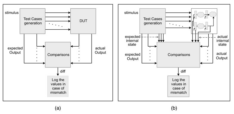
2.7.2.1 Black-box Testing
This is testing against specifications when the internal structure of the system is unknown. A set of inputs is applied and the outputs are checked against the specification or expected output, without considering the inner details of the system (Figure 2.18). The design to be tested is usually called the ‘device under test’ (DUT).
2.7.2.2 White-box Testing
This tests against specifications while making use of the known internal structure of the system. It enables the developer to locate a bug for quick fixing. Usually this type of testing is done by the developer of the module.
Figure 2.18 Digital system design testing using (a) the black-box technique and (b) the white-box technique
2.7.3 Levels of Testing in the Development Cycle
A digital design goes through several levels of testing during development. Each level is critical as an early bug going undetected is very costly and may lead to changes in other parts of the system. The testing phase can be broken down into four parts, described briefly below.
2.7.3.1 Module- and Component-level Testing
A component is a combination of modules. White-box testing techniques are employed. The testing is usually done by the developer of the modules, who has a clear understanding of the functionality and can use knowledge of the internal structure of the module to ease bug fixing.
2.7.3.2 Integration Testing
In integration testing, modules implemented as components are put together and their interaction is verified using test cases. Both black-box and white-box testing are used.
2.7.3.3 System-level Testing
This is conducted after integrating all the components of the system, to check whether the system conforms to specifications. Black-box testing is used and is performed by a test engineer. The testing must be done in an unbiased manner without any preconceptions or design bias. As the codings of different developers are usually integrated at the system level, an unbiased tester is important to identify faults and bugs and then assign responsibilities.
The first step is functional verification. When that is completed, the system should undergo performance testing in which the throughput of the system is evaluated. For example, an AES (advanced encryption standard) processor, after functional verification, should be tested to check whether it gives the required performance of encrypting data with a defined throughput.
After the system has been tested for specified functionality and performance, next comes stress testing. This stretches the system beyond the requirements imposed earlier on the design. For example, an AES processor designed to process a 2 Mbps link may be able to process 4Mbps.
2.7.3.4 Regression Testing
Regression testing is performed after any change to the design is made as a consequence of bug fixing or any modification in the design. Regression tests are a sub-set of test vectors that the designer needs to run after any bug fixing or significant modification in an already tested design. Both black-box and white-box methodologies are used. Fixing a bug may resolve the problem under consideration but can disturb other parts of the system, so regression testing is important.
2.7.4 Methods for Generating Test Cases
There are several methods for generating test cases. The particular choice depends on the size of the design and the level at which the design is to be tested.
2.7.4.1 Exhaustive Test-vector Generation
For a small design or for module-level testing, the designer may want to exhaustively generate all possible scenarios. How ever, the time taken by testing increases exponentially with the size of the inputs. For example, testing a simple 16 × 16-bit multiplier requires 216× 216 test vectors. The simulators can spend hours or even days in exhaustive testing of designs of even moderate size. The designer therefore needs to test intelligently, choosing sample points and focusing especially on corner cases. For mathematical computations, the overflow and saturation logic cases are corner cases. Similarly for other designs, the inputs that test the maximum strength of the system should be applied.
2.7.4.2 Random Testing
For large designs, the designer may resort to random testing. The values of inputs are randomly generated out of a large pool of possible values. In many instances this random testing should be biased to cover stress points and corner cases, while avoiding redundancy and invalid inputs.
2.7.4.3 Constraint-based Testing
Constraint-based testing works with random testing, whereby the randomness is constrained to work in a defined range. In many instances, constraint testing makes use of symbolic execution of the model to generate an input sequence.
2.7.4.4 Tests to Locate a Fault
In many design instances, the first set of input sequences and test strategies are used only to identify faults. Based on the occurrence and type of faults, automatic test patterns are generated that localize the fault for easy debugging.
2.7.4.5 Model Checkers
The designer can make use of models for checking designs that implement standard protocols (e.g. interfaces). Appropriate checkers are placed in the design. The input is fed to the model as well as to the design. When there is non-conformity the checkers fire to identify the location of the bug.
2.7.5 Transaction-level Modeling
Many levels of modeling are used in hardware design. RTL and functional-level modeling have already been mentioned. For functional-level modeling, algorithms are implemented in tools like MATLAB®, and in many design instances a design that is functionally verified is directly converted into RTL. However, designs are becoming more and more complex. This is especially the case for SoC and MPSoC, where more and more components are being added on a single piece of silicon. The inter working of the processors or other components on the chip is also becoming ever more critical. This inter working at register transfer level is very complex as it deals with bus protocols or NoC protocols. While analyzing the inter working of these components, usually this level of detail is not required and interworking can only be studied by observing the physical links to make complex packet or data transactions.
Transaction-level modeling (TLM) deals with designs that have multiple components. These components communicate with each other on some medium. At TLM, the detailed RTL functionality of the components and RTL protocol are not important. TLM separately deals with communications as transactions and the behavior of each component at the functional level. Transaction-level modeling is easy to develop and fast to simulate, so enabling the designer to verify the functionality of the design at transaction level early in the development life cycle. RTL models, though, are developed in parallel but are very slow to simulate for verification and analysis of the design. For a complex SoC design the architects need to develop these three models: the functional model in the early stages, while the transaction-level and RTL are developed in parallel. Building three models of a system requires them to be consistent at different stages of the design cycle.
2.8 Example of a Verification Setup
A complete setup for testing a signal-processing based design in hardware is shown in Figure 2.19. A C++ environment generates constrained random test vectors to be input to the algorithm running in C++ and also to the translated design that is implemented in TLM. A transactor block converts the test vector into transactions, and these are input to the transaction-level model. The output of the model is also in terms of transactions. A transactor converts the transactions into results that can be compared with the output of the simulation result. A checker compares the two results to find functional equivalence. The input to the simulator is also fed to a coverage block . This block checks the level of coverage and can direct the dynamic constrained random generator to generate the input sample to maximize the coverage.
When the transaction model of Figure 2.19(a) is verified, the same setup can be used to test the RTL design as in Figure 2.19(b). A driver block is added that converts a transaction into an RTL detailed signal to be input to the device under test (DUT). The output of the RTL implementation of the DUT is also converted back to transactions. A monitor checks the cycle-by-cycle behavior of the DUT using assertions.
2.9 SystemVerilog
As designs become more complex in functionality, test-vector generation for appropriate coverage is also becoming critical. Verification engineers have been using tools specific to verification, such as Vera and e .Nevertheless there has been a need to have a unified language that supports both design and verification of complex designs. SystemVerilog (SV) is such an initiative that offers a unified language that is very powerful to model complex systems and provides advanced level constructs. These constructs facilitate concise writing of test-benches and the analysis of coverage. Most of the EDA tool vendors are continuously adding support for SV. The added features make SV a very powerful language for hardware modeling and verification.
2.9.1 Data Types
SystemVerilog supports additional datatypes logic, int, bit, byte, longint and short-int . The data type reg of Verilog is ambiguous because reg also means a physical register but once inferred may result in a physical wire or a register. A logic type is similar to a reg where all the bits in the variable of this type can take any one of four values: 0, 1 , x and z . In the other data types each bit can be 0 or 1 . The variables of these types are automatically initialized to 0 at time zero. Table 2.13 shows all the additional data types in SystemVerilog and their related information.
Figure 2.19 Test setups for verification of a complex design that is implemented in C++, TLM and RTL. (a) Setup with TLM. (b) Same verification setup with TLM replaced by RTL DUT, a driver and a monitor block
Table 2.13 Additional datatypes in SystemVerilog
There are two ways to define an array in SV: packed and unpacked. SystemVerilog can operate on an entire two-dimensional (2-D) array of packed data, whereas the unpacked arrays can be operated only on an indexed value. The unpacked 1-D and 2-D arrays are declared as:
bit up_data [15:0];
bit [31:0] up_mem [0:511];
For packed cases the same arrays are declared as:
bit [15:0] p_data;
bit [31:0][0:511] p_mem1, p_mem2;
There are some constraints while operating on packed and unpacked arrays. The unpacked arrays can be sliced as:
slice_data = up_mem[2][31:15];
 // most significant byte at mem location 2
An operator can be applied on an entire packed array of data. An example is:
add_mem = p_mem1 + p_mem2;
Dynamic arrays can also be declared as:
bit [15:0] array[];
array = new[1023];
2.9.2 Module Instantiation and Port Listing
If the same names of ports are used in the instantiated module, the port names can be directly mentioned using <name> or can be simply skipped while only ports having different names are mentioned. Consider a module defined as:
module FA(in1, in2, sum, clk, rest_n);
Assuming the instance has the first three ports with the same name, the instance can be written as:
FA ff (.in1,.sum,.in2,.clk(clk_global),.rest_n (rst_n));
or more concisely as:
FA ff (.*,.clk(clk_global),.rest_n (rst_n));
2.9.3 Constructs of the C/C++ Type
SV supports many C/C ++ constructs for effective modeling.
2.9.3.1 typedef , struct and enum
The constructs typedef, struct and enum of C/C++ add descriptive power to SV. Their use is the same as in C. Examples of their use are:
typedef bit [15:0] addr;
 typedef struct {
 addr src;
 addr dst;
 bit [31:0] data;
 }packet_tcp;
module packet (input packet_tcp packet_in,
 input clk,
 output packet_tcp packet_out);
always_ff @(posedge clk)
 begin
 packet_out.dst <= packet_in.src;
 packet_out.src~ packet_in.data;
end
endmodule
The enum construct can be used to define states of an FSM. It can be used in place of the Verilog parameter or define . The first constant gets a value of 0. When a value is assigned to some constant, the following constants in the list are sequentially incremented. For example:
typedef enum logic [2:0]
{idle = 0,
read = 3,
dec, // = 4
exe // = 5} states;
states pipes;
The enum can also be directly defined as:
enum {idle, read=3, dec, exe} pipes;
case (pipes)
 idle: pc = pc;
 read: pc = pc+1;
.
.
endcase
2.9.3.2 Operators
The advanced features in SV enable it to model complex HW features in very few lines of code. For this, SV supports C-language like constructs such as:
operand1 OP = operand2
where OP could be +,—,*,/,%,>>,<<,>>>,<<<,&, | or^. For example, x = x + 3 can be written as:
x +=3;
SystemVerilog also supports post- and pre- increment and decrement operations + + x,x,x + + and x--
2.9.4 for and do-while Loops
SystemVerilog adds C/C++ type for and do-while loops. An example of the for loop is:
for(i=0, j=0, k=0; i+j+k<10; i++, j++, k++)
An example of the do-while loop is:
do
begin
if (sel_1 == 0)
 continue;
if (sel_2==3) break;
end
while (sel_2==0);
In this code, if sel_1 is zero, continue makes the program jump to the start of the loop at do . When sel_2 is 3, break makes the program exit the do-while loop, otherwise the loop is executed until the time sel_2 is zero.
2.9.5 The always Procedural Block
SV helps in solving the issue of the sensitivity list. There are several variants of the always block that give distinct functionality for inferring combinational or sequential logic. For a combinational block, SV provides always_comb . Similarly always_latch infers a latch. and always_ff realizes synchronous logic:
module adder(input signed [3:0] in1, in2,
 input clk, rst_n,
 output logic signed [15:0] acc);
 logic signed [15:0] sum;
// Combinational block
always_comb
 begin: adder
 sum = in1 + in2 + acc;
 end: adder
// Sequential block
always_ff @(posedge clk or negedge rst_n)
 if (!rst_n)
 acc <= 0;
 else
 acc <= sum;
endmodule
2.9.6 The final Procedural Block
The final procedural block is like the initial block in that it too executes only once, but at the end of the simulation. It is good for displaying a summary of results:
final
begin
 $display($time, “simulation time, the simulation ends
”);
end
2.9.7 The unique and priority Case Statements
In Verilog, while synthesizing the code, the user may need to specify the type of logic intended to infer from a case statement. The synthesis directives full-case and full-case parallel-case are used to indicate, respectively, whether the user intends the logic to consider the first match it finds in a case statement if there is a possibility of finding more than one match,or that the user guarantees that all cases are handled in the coding and each case will only uniquely match with one of the selections. This behavior is very specific to synthesis and has no implication on simulation. SV provides equivalent directives, which are unique and priority , to guarantees the simulation behavior matches with the intended synthesis results. The examples below explain the two directives:
always @*
unique case (sel) //Equivalent to full-case parallel-case synthesis directive
 2’b00: out = in0;
 2’b01: out = in1;
 2’b10: out = in2;
 2’b11: out = in3;
 default: out = x;
endcase
The priority caseis used in instances where the programmer intends to prioritize the selection and more than one possible match is possible:
always @*
priority case (1’b1) //equivalent to full-case synthesis directive
 irq1: out = in0;
 irq3: out = in1;
 irq2: out = in2;
 irq4: out = in3;
 default: out= ‘x;
endcase
2.9.8 Nested Modules
SV supports nested modules, so that a module can be declared inside another module. For example:
module top_level;
module accumulator(input clk, rst_n, input [7:0] data, outputbit [15:0] acc);
always_ff @ (posedge clk)
begin
 if (!rst_n)
 acc <= 0;
else
 acc <= acc + data;
end
endmodule
logic clk=0;
always #1 clk = ~clk;
logic rst_n;
logic [7:0] data;
logic [15:0] acc_reg;
accumulatoracc_inst(clk, rst_n, data, acc_reg);
initial
begin
 rst_n = 0;
 #10 rst_n = 1;
 data = 2;
 #200 $finish;
end
initial
$monitor($time, "%d, %d
", data, acc_reg);
endmodule
2.9.9 Functions and Tasks
SVenhances Verilog functions and tasks with more features and flexibility. No begin and end is required to place multiple statements in functions and tasks. Unlike with a function in Verilog that always returns one value, SV functions can return a void . Use of the return statement is also added, whereby a function or a task returns a value before reaching the end. In SV, the input and output can also be passed by name; and, in a similar manner to module port listing, default arguments are also allowed.
The following example shows a function that returns a void :
function void expression (input integer a, b, c, output integer d);
 d = a+b-c;
endfunction: expression
Below is another example that illustrates a function returning before it ends:
function integer divide (input integer a, b);
 if (b)
 divide = a/b;
 else
 begin
 $display(‘‘divide by 0
’’);
 return (’hx);
 end
 // Rest of the function
.
.
 endfunction: divide
2.9.10 The Interface
The interface is a major addition in SV. The interface encapsulates connectivity and replaces a group of ports and their inter working with a single identity that can be used in module definition. The interface can contain parameters, constants, variables, functions and tasks. The interface provides a higher level of abstraction to users for modeling and test-bench generation.
Consider two modules that are connected through an interface, as shown in Figure 2.20. The roles of the ports input and output change from one interconnection to the other. The modport configures the direction on ports in an interface to be an input or output.
interface local_bus(input logic clk);
bit rqst;
bit grant;
bit rw;
bit [4:0] addr;
wire [7:0] data;
modport tx (input grant,
 output rqst, addr,rw,
 inout data,
 input clk);
modport rx (output grant,
 input rqst, addr, rw,
 inout data,
 input clk);
endinterface
module src (input bit clk,
 local_bus.tx busTx);
integer i;
logic [7:0] value = 0;
assign busTx.data = value;
initial
begin
 busTx.rw = 1;
 for (i=0; i<32; i++)
 begin
 #2 busTx.addr = i;
 value += 1;
end
busTx.rw = 0;
end
// Rest of the module details here
module dst (input bit clk,
local_bus.rx busRx);
logic [7:0] local_mem [0:31];
always @(posedge clk)
 if (busRx.rw)
 local_mem[busRx.addr] = busRx.data;
endmodule
// In the top-level module these modules are instantiated with interface
declaration.
 module local_bus_top;
logic clk = 0;
local_bus bus(clk); // the interface declaration
always #1 clk = ~clk;
 src SRC (clk, bus.tx);
 dst DST (clk, bus.rx);
initial
$monitor ($time, "	%d%d %d %d
", bus.rx.rw, bus.rx.addr,
 bus.rx.data, DST.local_mem[bus.rx.addr]);
endmodule
Figure 2.20 Local bus interface between two modules
2.9.11 Classes
In SV, as in C++, a class consists of data and methods. The methods are functions and tasks that operate on the data in the class. SV supports key aspects of object-oriented programming (OOP), including inheritance, encapsulation and polymorphism.
A class is declared with internal or external declared functions that operate on the data defined in the class. The example below defines a class with an internal and external declared method:
class frame{
byte dst_addr;
bit [3:0] set_frame_type;
data_struct payload;
function byte get_src_addr ()
 return src_addr;
endfunction
extern task assign_dst_addr_type (input byte addr, input bit[3:0] type);
endclass
task frame::assign_dst_addr(input byte addr, input bit [3:0] type);
 dst_addr = addr;
 frame_type = type;
endtask
The syntax only declares an object class of type frame. One or multiple instances of this class can be created as follows:
frame first_frame = new;
A class constructor can also be used to initialize data as:
class frame
function new (input byte addr, input [3:0] type)
 dst_addr = addr;
 frame_type = type;
endfunction
.
.
endclass
// Set the dst and type of the frame
frame msg_frame = new(8’h00, MSG);
Another class can inherit data and methods of this class and adds new methods and can change the existing methods.
class warning_frame extends frame;
bit [2:0] warning_type;
function MSG_TYPE send_warning ();
 return warning_type;
endfuction;
endclass
Using object-oriented programming (OOP), the classes defined in OVM and VMM can be extended for effective verification. For example, vmm_data class has many member functions, including set_log (), display(), copy() and compare() [15]. These methods can be used and new methods can be added by extending this base class:
class burst_frame extends vmm_data;
SV restricts inheritance to single inheritance only. The derived class can override the methods of the parent class. The derived class can also use members of the parent class with a keyword super:
class abs_energy;
 integer amp;
function integer energy ();
 energy = amp*amp;
endfunction
endclass
A derived class can be declared that overrides the function energy:
class mod_energy extends abs_energy;
integer amp;
function integer energy();
 energy = 0.5*super.energy() + amp * super.amp;
endfunction
endclass
SValso supports data hiding and encapsulation. To restrict the scope of a member to the parent class only, the member is declared as local or protected. The local members are accessible only to methods defined inside the class, and these members cannot be inherited by derived classes as they are not visible to them. A protected method can be inherited by a derived class.
Virtual classes or methods in SV provide polymorphism. These classes are used to create a template. Using this template, real classes are derived. The virtual methods defined in a virtual class are overridden by the derived classes:
virtual class frame;
ip frame,
atm frame,
stm frame
virtual class frame;
virtual function integer send (bit [255:0] frame_data);
endfunction
endclass
The derived classes are:
class ethernet extends frame;
function integer send (bit [255:0] frame_data);
// The contents of the function
.
.
endfuntion
endclass
class atm extends frame;
frame gateway_frame [10];
Frames of various types can be declared and assigned to the array:
ethernet frame_e = new;
atm frame_a = new;
gateway_frame [0] = frame_e;
gateway_frame [1] = frame_a;
The statement
gateway_frame [1].send();makes the compiler finds out which frame will be sent.
2.9.12 Direct Programming Interface (DPI)
SV can directly access a function written in C using a DPI. Similarly a function or task written in SV can be exportedto a C program. SV makes interworking of C and SVcode very trivial and there is no need to use PLI. The C functions in SV are then called using import directive, while functions and tasks of SV to be used ina C function are accessible by using export DPI declaration. The illustration here shows DPI use:
// top-level module that instantiates a module that calls a C function
module top_level();
moduleCall_C Call_C (rst, clk, in1, in2, out1,…
.
.
.
endmodule
The instantiated module Call_C of type moduleCall_C uses an import directive for interfacing with a C program:
module moduleCall_C(rst, clk, in1, in2, out1,…;
.
.
import "DPI-C" context task fuctionC (….);
always@(posedge clk)
 functionC (rst,in1, in2, out1,….);
 export "DPI-C" task CallVeri1;
 export "DPI-C" task CallVeri2;
task CallVeri1 (input int addr1, output int data1);
.
.
endtask
.
.
task CallVeri2 (input int addr2, output int data2);
.
.
 endtask
 endmodule
The C function functionC is called from the SV module, and this function further callsfunct1 () and funct2(). These two functions use tasks CallVeri1 and CallVeri2 defined in SV:
// required header files
void fuctionC (int rst,….)
{
.
.
 rest = rst;
.
 funct1(…);
 funct2(…);
.
.
}
void funct1 (void)
{
.
.
 CallVeri1(….);
.
}
void funct2 (void)
{
.
.
 CallVeri2(….);
.
}
2.9.13 Assertion
Assertion is used to validate the behavior of a design. It is used in the verification module or in an independent checker module. SV supports two types of assertion, immediate and concurrent. The immediate assertion is like an if-else statement. The expression in assert is checked for the desired behavior. If this expression fails, SV provides that one of the three severity system tasks can be called. These tasks are $warning, $error and $fatal . The user may also use $info where no severity on assertion is required. Below is an example:
assert(value>=5) else $warning(“Value above range”);Concurrent assertion checks the validity of a property. There are several ways to build properties; these may be compound expressions using logical operators or sequences:
assert property (request && !ready)An example of a sequence is:
assert property (@posedge clk) req |–> ##[2:5] grant);Here, the implication operator (|–>) checks on every posedge of clk the assertion of req , and when it is asserted then the grant must be asserted in 2 to 5 following clock cycles.
2.9.14 Packages
SV has borrowed the concept of a package from VHDL. By using package , SV can share user-defined type definitions across multiple modules, interfaces, other programs and packages. The package can contain, for example, parameters, constants, type definitions, tasks, functions, import statements from other packages and global variables. Below is an example:
package FSM_types
// global typedef
typedef enum FSM{INVALID, READ, DECODE, EXECUTE, WRITE} pipelines;
 bit idle; // global variable initialize to 0
 task invalid_cycle (input [2:0] curret_state) //global task
 if (current_state == INVALID)
 $display(“invalid state”);
 $finish;
 endtask: invalid_cycle
endpackege
2.9.15 Randomization
SV supports unconstrained and constrained random value generation. The function randomize returns 1 if it successfully generates the constrained random value, otherwise it returns 0.
bit [15:0] value1, value2;
bit valid;
initial
begin
 for(i=0; i<1024; i++)
 valid = randomize (value1, value2);
 end
end
The randomization can also be constrained by adding a with clause. The example given above can be constrained as:
valid = randomize (value1, value2); with (value1>32; value1
2.9.16 Coverage
The coverage in SV gives a quantitative measure of the extent that the functioning of a DUT is verified is the simulation environment. The statistics are gathered using coverage groups. With a coverage group, the user lists variables as conver points . The simulator collects statistics of the values these variables take in simulation. The simulator stores the values of these variables in a coverage database.
module stimulus;
logic [15:0] operand1, operand2;
.
.
covergroup cg_operands @ (posedge clk)
 o1: coverpoint = operand1;
 o2: coverpoint = operand2;
endgroup: cg_operands
.
.
.
cg_operands cover_ops = new();
.
endmodule
Each coverage point contains a set of bins. These bins further refine the values the variable takes for each range.
covergroup cg_operands @ (posedge clk)
 o1: coverpoint = operand1 {
 bins low = {0,63};
 bins med = {64,127};
 bins high = {128,255};
 }
 o2: coverpoint = operand2 {
 bins low = {0,63};
 bins med = {64,127};
 bins high = {128,255};
 }
endgroup: cg_operands.
The coverage group can be used inside a module, class or interface.
Exercises
Exercise 2.1
Write RTLVerilog code to implement the design given in Figure 2.21. Generate the appropriate reset signal for the feedback register used in the design. Develop a test plan and write a stimulus to test the design for functional correctness. Also write a test case to count the number of cycles it takes for the register out_reg to overflow for in1 and in2 and sel set to 1. Also, code the design and stimulus in SystemVerilog.
Figure 2.21 Digital design at register transfer level with a feedback register
Exercise 2.2
Design an ALU data path that performs the following operations in parallel on two 16-bit signed inputs A and B and assigns the value of one of the outputs to 16-bit C. The selection of operation is basedona2-bit selection line. Code the design in both Verilog and SystemVerilog. Write test vectors to verify the implementation.
C=A+B C=A-B C=A&B C=A|BExercise 2.3
Code the logic of the following equations in RTL Verilog:
acc0 = acc1 + in1; acc1= acc0 + in2; out = acc0 + acc1;where in1 and in2 are two 32-bit inputs, out is a 40-bit output, and acco and acc1 are two 40-bit internal registers. At every positive edge of a clock the inputs are fed to the design and out is produced.
Figure 2.22 Digital design at register transfer level showing the combinational and synchronous components
Exercise 2.4
Write RTL Verilog code of the module device_under_test given in Figure 2.22. Four 8-bit inputs, in1, in2, in3 and in4, are input to four 8-bit registers, R0, R1, R2 and R3 , respectively, at every positive edge of the clock. Four values in these registers are added, and bitwise AND operation is performed on the values stored in these registers to produce out_1 and out_2 .
Exercise 2.5
Write an RTL Verilog code and its stimulus to implement and test the module device_ under_test given in Figure 2.23. The inputs and outputs of the module are shown. Generate a 20-time unit clock clk from the stimulus, as well as a rst_n signal to reset the device before the first positive edge of the clock. The widths of each input and output signals are shown. Write test vectors by varying all the input signals in each test. Make sure each test vector is valid only for one clock period. Use the monitor statement to print the values of the inputs and outputs on the screen. Finally, rewrite the stimulus in SystemVerilog and use coverage to test the design for selective ranges of input values. Use data paths of exercise 2.2 for the ALU.
Exercise 2.6
Design a data path with three 8-bit accumulators. The first accumulator, acc1 , adds a 4-bit input data in acc1 in every clock cycle. The second accumulator, acc2 , adds the first accumulator in itself, and the third accumulator, acc3 , adds the first and second accumulators in itself in every clock cycle. Each accumulator has an asynchronous reset. Draw the RTL-level diagram and code the design in RTL Verilog.
Figure 2.23 Digital design with multiple inputs and outputs
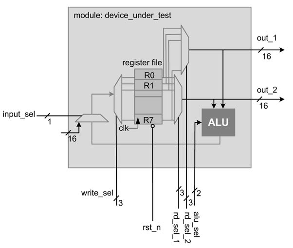
Exercise 2.7
Write RTL Verilog code to implement the design given in Figure 2.24. The feedback register needs to be reset using a negative-level asynchronous reset. Write a stimulus for the design. The out is the output of the module, and in is the input. Identify other signals that need to be defined as ports of the module.
Figure 2.24 RTL design of a digital circuit
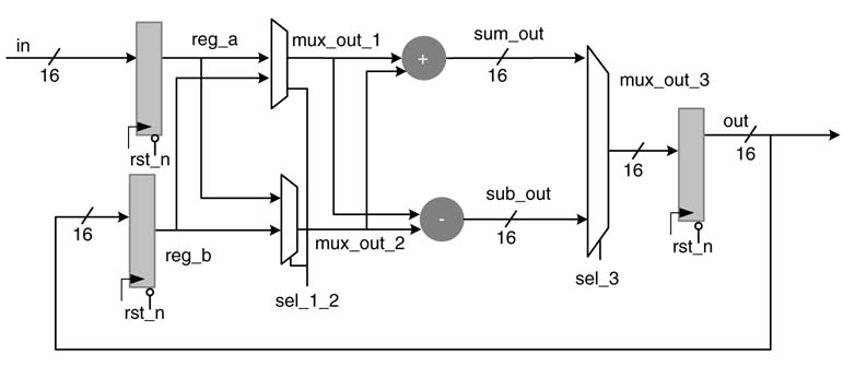
Exercise 2.8
Draw an RTL diagram for the following Verilog code. Clearly specify the data widths of all the wires, and show multiplexers, registers, reset and clock signals.
module test_module (input [31:0] x0, always @ (posedge clk or negedge
input [1:0] sel, input clk, rst_n) begin
 rst_n, output reg [31:0] y0); if(!rst_n) begin
reg [31: 0] x1, x2, x3; y1 <=0;
reg [31: 0] y1; y0 <=0;
wire [31:0] out; end
assign out = (x0 + x1 + x2 + x3 + y1)>>>2; else begin
always @(posedge clk or negedge rst_n) y1 <= y0;
begin y0 <= out;
 if(!rst_n) begin end
 x1 <=0; end
 x2 <=0; endmodule
 x3 <= 0;
 end
 else if (sel==0) begin
 x3 <= x2;
 x2 <= x1;
 x1 <= x0;
 end
 else if (sel == 01) begin
 x3 <= x1;
 x2 <= x0;
 x1 <= x2;
 end
 else begin
 x3 <= x3;
 x2 <= x2;
 x1 <= x0;
 end
end
Exercise 2.9
Partition the RTL-level design given in Figure 2.25 into two or three modules for better synthesis result. Write RTL Verilog code for the design. For the combinational cloud, write an empty function or a task to implement the interfaces.
Exercise 2.10
Design architecture, and implement it in RTL Verilog to realize the following difference equation:

Implement multiplication with 0.5 and 0.25 by shift operations.
Figure 2.25 Digital design with combinational clouds for different design objectives
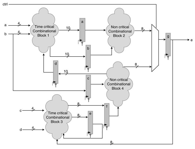
References
1. S. Palnitkar, Verilog HDL , 2nd edn, Prentice-Hall, 2003.
2. M. D. Ciletti, Advanced Digital Design with the Verilog HD , Prentice-Hall, 2003.
3. Z. Navabi, Verilog Digital System Design: Register Transfer Level Synthesis, Testbench, and Verification, McGraw-Hill, 2006.
4. IEEE, Standard 1364-1995: “Hardware description language based on Verilog,” 1995.
5. IEEE, Standard 1364-2001: “Verilog hardware description language,” 2001.
6. “SystemVerilog 3.1, ballot draft: Accellera’s extensions to Verilog,” April 2003.
7. IEEE, Standard 1364 -2005: “Verilog hardware description language,” 2005.
9. M. Keating and P. Bricaud, Reuse Methodology Manual for System-on-a-Chip Designs, 3rd edn, Kluwer academic Publishers, 2002.
10. IEEE, Standard 1800-2005: “SystemVerilog: unified hardware design, specification and verification language,” 2005.
11. www.xilinx.com
12. V. Berman, “IEEE P1647 and P1800: two approaches to standardization and language design,” IEEE Design & Testing of Computers, 2005, vol. 22, pp. 283–285.
13. Accellera Standards, Verification Intellectual Property (VIP) Recommended Practices, vol. 1.1, August 2009.
14. A.Alimohamnnad, S. F. Fard and B. F. Cockburn, “FPGA-based accelerator for the verification of leading-edge wireless systems,” in Proceedings of Design Automation Conference, 2009, ACM/IEEE, pp.844–847.
15. www.ovmworld.org