
CHAPTER 5
Schematic Design
When designing simple projects, or projects that simply add inputs and outputs to a mirocontroller, you can often work directly from the breadboard design. If you work like this, you probably want to stay away from the Schematic tab, because if you look at it, it will probably be a mess with components all over the place.
As soon as projects become just a little bit complex, or you want to share your design with someone, then an easy-to-read schematic is necessary. Once you are familiar with schematic diagrams, you may find it easier to start with a schematic and then move on to the Breadboard view.
Reading Schematic Diagrams
Before we can reasonably expect to draw schematic diagrams, we need to be able to read them and at least get the gist of what they are saying. Although schematics look difficult to understand, there are conventions that make them easier to read.
The lines on a schematic represent an electrical connection, be it a wire or a clip on the breadboard or a copper track on the surface of the PCB. These lines link the components that make up the circuit.
Component Symbols
Component symbols don’t generally look like the actual components. They are symbolic representations of the components and therefore say more about how the components operate than what they look like. The resistor symbol is a good case in point. Its zigzag line looks like something that might resist the flow of current.
Table 5-1 shows some of the most common components.
TABLE 5-1 Common Schematic Symbols
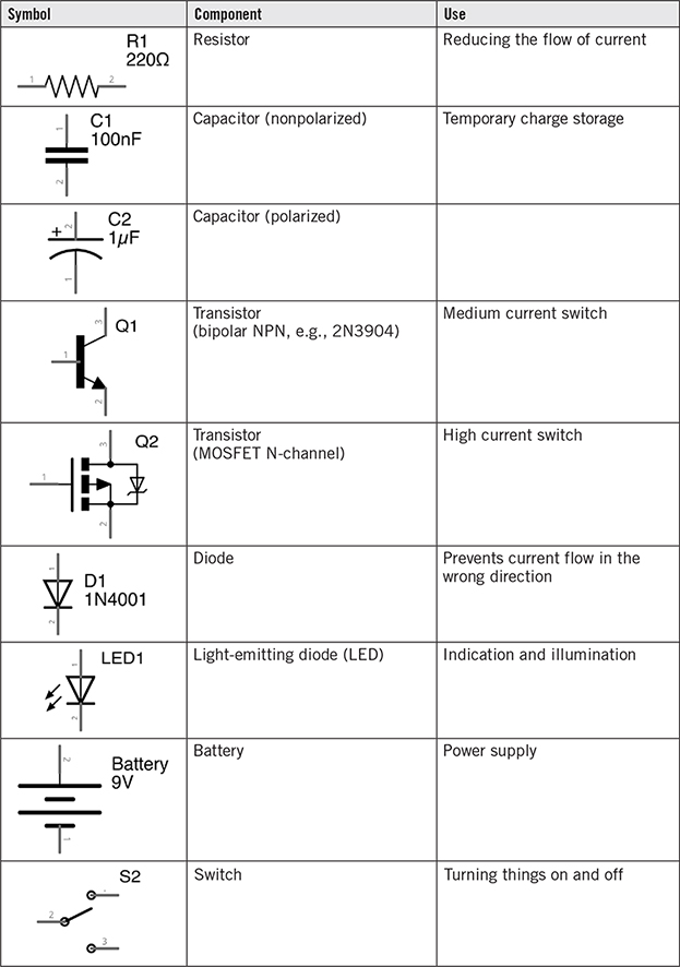
In this book, we will use the same circuit symbols as in Fritzing. These are based on the U.S. standard of component symbols. Europe has a slightly different set of symbols, the main difference being that in the European system, resistors are represented as rectangles rather than zigzag lines.
Schematic Versus Breadboard
Figure 5-1 shows the schematic diagram (Figure 5-1a) and the breadboard layout for the same project (Figure 5-1b) side by side, so that you can compare the two representations.
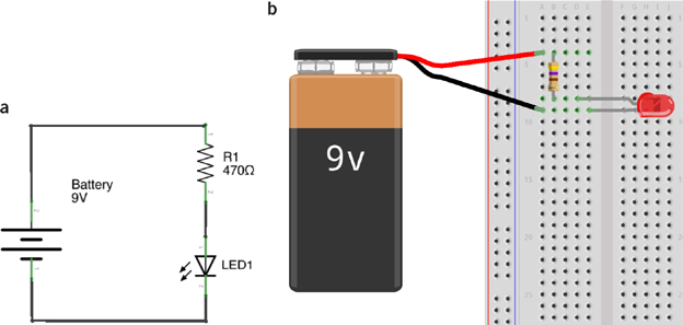
FIGURE 5-1 Schematic and breadboard diagrams.
In this case, relating the two diagrams is easy, because the components are more or less in the same place.
Conventions
In theory, you can place the components in a schematic in any crazy positions you like and connect them by the most bizarre connections, and it will still be a perfectly valid way of drawing the circuit. Figure 5-2 shows an example of such madness.
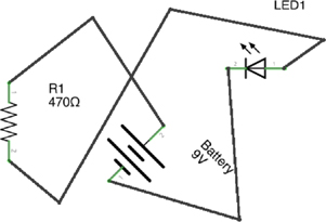
FIGURE 5-2 A mad schematic diagram.
First Rule of Schematics: Straight Lines at Right Angles
Electronics engineers tend to be quite tidy in their work. Schematic diagrams are drawn with straight lines at right angles to one another. Lines are allowed to cross one another on the diagram, but if the lines are to be joined together where they cross, then a dot is placed over the junction of the wires.
Second Rule of Schematics: Positive Voltages Uppermost
It is a convention that most people follow, when they draw a schematic, to put the higher voltages near the top, so that on the left-hand side of the diagram, we have a 9V battery. The bottom of the battery is at 0V or GND or Ground, and the top of the battery will by 9V higher than that.
Notice that we draw the resistor R1 above the LED (LED1), so we can think of the current flowing through the resistor, before flowing through the LED and then back to the negative connection of the battery.
Third Rule of Schematics: Things Happen Left to Right
Western civilization invented electronics, and it writes from left to right. You read from left to right, and culturally speaking, more things happen from left to right. Electronics is no different, so it is common to start with the source of the electricity—the battery or power supply on the left—and then work our way from left to right across the diagram.
Fourth Rule of Schematics: Group-Related Components
Keep components that are functionally related to one another close to one another. For example, keep the current-limiting resistor for an LED close to the LED.
Names and Values
It is a good idea to give every component in a schematic a name. So, in this case, the battery pack is called just Battery, the resistor is R1, and the LED is LED1. This means that when you go from a schematic to a breadboard layout and eventually a circuit board, then you can see which components on the schematic correspond to which components on the breadboard or circuit board.
It is also usual to specify the value of each of the components, where appropriate. So, for example, the resistor’s value of 470Ω is marked on the diagram.
Tidying a Schematic in Fritzing
If you followed my advice in Chapter 4 and drew the breadboard layout shown in Figure 4-12, you should now have a Fritzing project with a breadboard layout that looks like Figure 5-3a; and if you switch to the Schematic tab on that project, it should look something like Figure 5-3b.
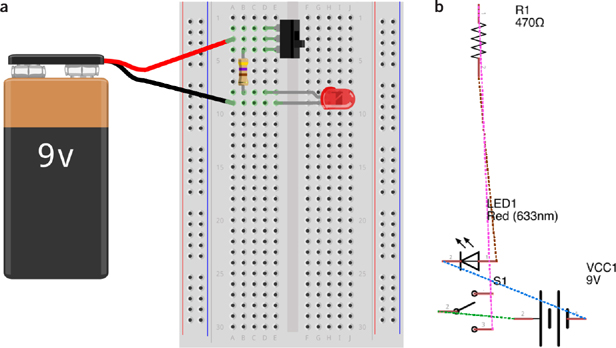
FIGURE 5-3 Starting point for schematic tidying.
The layout of Figure 5-3b is the default layout made by Fritzing on your behalf as you drew the breadboard layout. It’s a bit of a mess, but that’s okay because you will now tidy up this schematic one step at a time.
Step 1. Position the Components
I like to start by moving the components around, so that they follow the left-to-right and higher voltages at the top rules that we discussed earlier. It’s easier to get things lined up and your lines at right angles if you turn on Align to Grid in the View menu. Start by rearranging the components as shown in Figure 5-4.
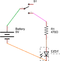
FIGURE 5-4 Components in the right place.
Move the battery over to the left, and rotate it so the positive connection is at the top. Next, position the switch, the resistor, and the LED, rotating where necessary. At this point, you can also right-click on the LED and deselect the option to display the LED’s color attribute. Also double-click the battery’s current name (VCC1) and rename it Battery.
You can rotate the text of the labels independently of the component as a whole by using the menu that pops up when you right-click on the label. You will need to do this for the battery and the LED.
You can also move the labels around relative to the position of the component just by selecting the label and then dragging it.
Step 2. Routing the Nets
Each of the lines on the schematic is called a net. In fact, were there any places in this schematic where there were lines that were connected, they would all be part of one net. Initially, in the Schematic view, the component leads are connected with dashed lines to indicate that these lines have not yet been routed. That is, we have not drawn proper lines between them.
Although you can ask Fritzing to route the schematic for you by using the Autoroute option on the Routing menu, it does not always work perfectly, so it’s better to do this task by hand.
The easiest way to do this is to drag a line out from one of the leads to its connection to another component along the route you want it to take. Figure 5-5a shows this for the connection between the negative battery lead and the LED. When you let go of the mouse button, the line will appear between the two component leads. You can also add a bend point in the line by double-clicking on the line and then dragging the bend point where you want it.
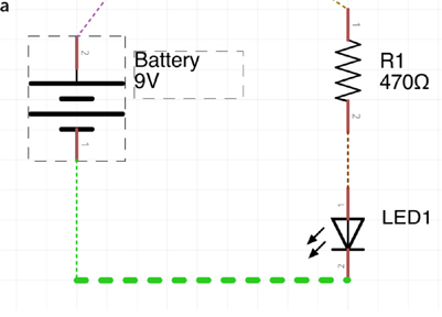
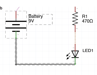
FIGURE 5-5 Routing a net.
If the dashed line that needs turning into a wire is just a straight line, then double-clicking on the dashed line will convert it.
When all the lines are added, the schematic will look like Figure 5-5b.
Creating a Schematic in Fritzing
In the situation where you are starting with a blank schematic, creating the schematic involves most of the same skills that you use when you are tidying a schematic created from a breadboard design. There is, however, an additional first step of adding the components that you need.
In Chapter 2, we briefly used an example of a 555 timer project to illustrate drawing a schematic. In this example we will take that initial design and modify it to use multiple flashing red LEDs as a rear cycle lamp. The basic design is much the same as that of project 2, so we will begin with a schematic design and then move on to the PCB design for this project in Chapter 6.
If you followed along with the quick-start chapter, you should find it easy to follow these instructions to create the schematic for this project. The end result that you are aiming for is shown in Figure 5-6. You may wish to create this without following the step-by-step instructions, but revert to the instructions if things go wrong.
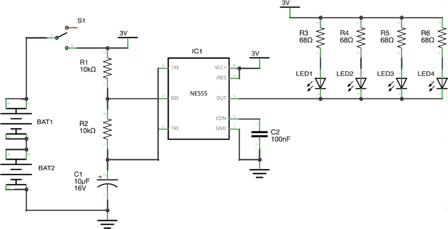
FIGURE 5-6 Schematic for rear bicycle light.
Design Calculations
Before we wade into the schematic design proper, there are a few design calculations that we need to make. If you are completely new to electronics, then these may seem a little advanced. Since this book is primarily about using Fritzing rather than electronic design, you may find it useful to have a look at a basic electronics text such as Hacking Electronics or Make: Electronics.
It would be very nice to power this project from the cheap and readily available AAA batteries. These are small, but not so small that they won’t last a decent while. You can do a rough calculation of how long a battery will last by using Table 5-2 to look up the capacity of the battery in milliampere-hours (abbreviated as mAh). That figure is the number of hours that the battery can supply a current of 1mA.
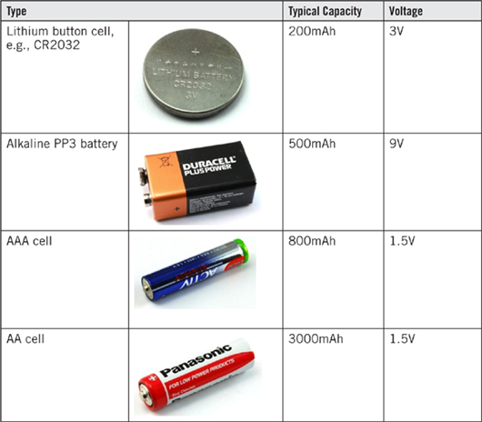
From this you can see that a AAA battery can supply 1mA for approximately 800 hours. This is very approximate, as there are no guarantees for batteries, especially if they have been on the shelf for a while. Now, we have 4 LEDs, and if we assume 20mA per LED, that makes 80mA. But then the LEDs are also flashing, so if we assume they are on only one-half of the time, then there will be an average current draw of around 40mA. The 555 timer chip will use a pretty small amount of current too, but let’s ignore that for now.
So now our AAA battery will last 800/40 = 20h. This is a pretty respectable amount of time. A single AAA battery will only generate a voltage of around 1.5V, but the 555 timer will not operate on such a low voltage, so we will have two batteries one after the other (called in series). This will give a total voltage of 3V.
In fact, even 3V is not enough for a standard 555 timer (the NE555) that requires at least 4.5V. Fortunately for us there is a variation of the 555 timer called the TLC555 that operates in exactly the same way as the 555 timer, but only needs 2V or more to operate.
When you used the 555 timer back in Chapter 2, there was no discussion about how to control the speed at which the LEDs flashed. In fact, the frequency of flashing is determined by the values of R1, R2, and C1 in Figure 5-6. There is a formula for this, which you will find if you look at the datasheet for the 555 timer, but it’s a lot easier to use an online calculator such as the one at www.ohmslawcalculator.com/555_astable.php. This is also shown in Figure 5-7.
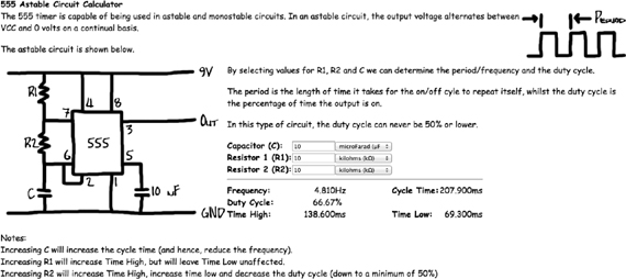
FIGURE 5-7 A 555 timer calculator.
Here C1 is just called C, and there are fields where you can enter values for C, R1, and R2. When you do so, the fields underneath these three fields automatically update themselves. So you can see that with a C value of 10µF and resistors both of 10kΩ, the frequency will be 4.8Hz. That means almost 5 flashes per second. This is probably about the right flash rate.
The Duty Cycle field is underneath the Frequency field. This indicates what proportion of the time the 555 timer’s output is high. This is not automatically 50 percent and allows you to make short-duration pulses rather than even flashing if you want. The Time High and Time Low figures express this same information in a different way. If you look at Figure 5-6, you can see that LEDs have one end connected to the positive battery supply via current-limiting resistors. This means that the 555 timer will turn on the LEDs when its output goes low and the voltage flows from the higher voltage to the lower. The LEDs will therefore be on for 69.3ms of the total 207.9ms for each cycle. This means that the LED will be off slightly longer than it is on for each cycle (on one-third of the time). The advantage of this is that our battery will last a bit longer than our earlier calculation would suggest.
It is quite fun to try a bit of trial and error with the component values and see what effect this has on the operation of the project. You should, however, bear in mind that not every single possible value of resistor or capacitor is available. Nor are the actual values exact. For instance, capacitors often only have an accuracy of 10 or 20 percent, so your flashes may vary a little from one build of the project to the next. In this case, that does not matter at all.
Common values of resistors and capacitors are listed in the Appendix.
The final component calculation that we need to make is the value of the current-limiting resistors for each of the LEDs. For this you can refer to Table 4-1. We want the LEDs to be as bright as possible, so let’s use 68Ω resistors, equivalent to a current of 20mA.
Drawing the Schematic
The following sections will lead you through the drawing of the schematic one step at a time. To gain practice drawing schematics, follow along; or if you get fed up with that, the Fritzing file for this project can be found in the file cycle_lamp_example.fzz along with all the other Fritzing projects used in this book. These can all be downloaded from the author’s website at simonmonk.org. Just follow the links for this book.
Step 1. Add the 555 Timer
If a design is centered about a chip, as it is in this case, then I like to start by positioning it in the center of the design.
Switch to the Schematic tab and use the search facility in the parts bin. Use 555 as the search term. This will bring a few results. Look for the one shown in Figure 5-8. This one is from Sparkfun and names the pins rather than just identifying them by pin number, so it makes for a more meaningful schematic.
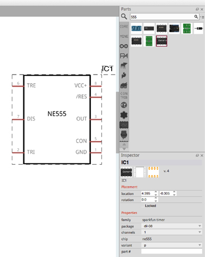
FIGURE 5-8 Adding a 555 timer part to the schematic.
Note that the part is labeled NE555. Earlier in this chapter, it was decided that it would be better to use the TLC555 variant of the 555 timer, because of its lower voltage compatibility. There is no TLC555 part in the parts bin, so we will use an NE555 instead. The label NE555 is actually part of the image file used with the part, so it is not so easily changed. However, in Chapter 9, I will show you how to modify and create new parts, so that we can have the right label on our schematic.
Step 2. Add the Timing Components
Having put the IC down, you should start by adding the timing components R1, R2, and C1 to the schematic. These can all be found in the CORE section of the parts bin. The capacitor is of the electrolytic variety. Drag the three components onto the schematic diagram, and rotate the two resistors by 90°. The capacitor is already in the correct orientation.
Once the components are in roughly the right positions, set the component values. Both resistors should be given values of 10kΩ using the resistance field in the Inspector. The capacitor actually has two values that need to be set. The capacitance should be set to 10µF and the voltage to 16V. Use the drop-down lists to select these values. The drop-down lists are populated with standard values for these components, so if you are not sure about what values are common, you can use the drop-down lists to allow Fritzing to tell you.
The capacitor has two values: the capacitance, which is obvious, but it also has a voltage value. This value is the maximum voltage that the capacitor can cope with. If this voltage is exceeded, then the capacitor is likely to fail. So generally it’s a good idea to err on the side of caution and in this case select 16V from the drop-down list of standard voltage values. In actual fact, the lowest number in the drop-down list (6.3V) would be fine too.
Rotate the labels of the two resistors by 90° clockwise, and then drag all three labels neatly to the left of their respective components. To rotate the label of a component without rotating the whole component, first select the component and then right-click over that component’s label, select Flip/Rotate | 90 Degrees Clockwise.
When all this is complete, the schematic will look something like Figure 5-9.
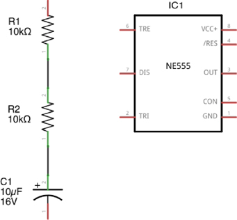
FIGURE 5-9 Adding the timing components.
Step 3. Connecting the Timing Components
Drag the connector for the bottom lead of R1 to the top lead of R2. When they connect properly, both connectors will turn green. Connect R2 and C1 in the same way.
Each of these lines connecting components is called a net. Even if it’s just a single line, it’s still called a net. We need to add a connection between pin 7 (DIS) of the IC1 timer to the net that we have just made between R1 and R2. If you try to drag out from pin 7 of the timer IC, then Fritzing will ignore the line that you want to connect to. It will let you connect to either end of the line, but really we want to connect right in the middle of the line.
The trick to doing this is illustrated in Figure 5-10.
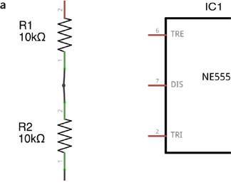
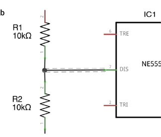
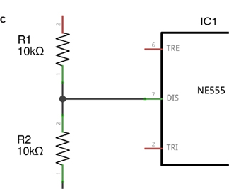
FIGURE 5-10 Adding a connection to an existing net.
First, add a bend point to the line roughly where you want to join the net (Figure 5-10a) by double-clicking on the line. Then drag out from the DIS pin of IC1 to the new bend point. This is likely to be a bit crooked, so finally grab the bend point and drag it so that it is square (Figure 5-10c). This should be done with the Align to Grid feature turned on (on the View menu). Notice how there is a big dot over the junction. This is important; it tells you that all the lines leading off from that dot belong to the same net. If there is no big dot, then there is no connection and this will cause you problems later when you come to make a PCB layout.
You need another junction midway between R2 and C1, so make a bend point there in the same way as you did between R1 and R2. This connection needs to go to pin 2 (TRI) of IC1. Here you drag a line directly from pin 2 of IC1 to the bend point between R2 and C1, and then add a bend point to make the lines at right angles.
Pin 6 also needs to be connected to pin 2, which you can do by simply dragging from the tip of pin 6 to the tip of pin 2. The end result of this is shown in Figure 5-11.
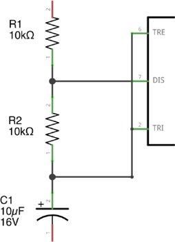
FIGURE 5-11 Connecting pins on IC1.
Notice how there is now a little dot on the end of pin 2, but importantly, where the line from pin 6 to pin 2 crosses pin 7, note that there is no dot. That’s good, because there should not be a connection here.
A good trick to reassure yourself that things you think are connected are really connected is to move a part and make sure that the connection lines to it move with it when you drag it.
Step 4. Adding Power Symbols
In any schematic, there are always two special nets. One is the ground net. Ground or sometimes GND or 0V is the baseline voltage. This will usually be connected to the negative end of a battery for battery-powered equipment, and the other is the positive supply for the circuit. These nets usually connect to lots of parts in the design. As a schematic gets more complex, it can be tricky to connect everything with lines, especially these power nets.
To make things neater, special stand-in symbols are used for the GND and positive supply. You do not have to use them, but if you do, it makes for easier-to-read schematics. You will find these special symbols in the Schematic View section of the CORE parts bin. Drag on one ground connection and one V++ symbol. Change the voltage property of the V++ symbol to 3V, and connect them to the top of R1 and the bottom of C1, as shown in Figure 5-12.
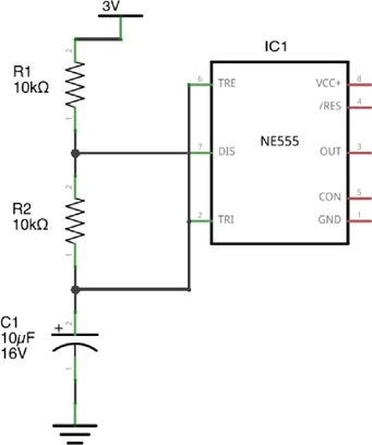
FIGURE 5-12 Adding supply symbols.
Step 4. Connecting C2 and More Power Symbols
Drag a capacitor (ceramic this time) onto the schematic area to the right of and below the IC. Then duplicate the ground and 3V symbols (Duplicate is an option on the right-click menu, or type CTRL-D), positioning them to the right of IC1, then connect them. Duplicating a component or power symbol has the advantage that its properties are carried along with it, so you do not need to change the voltage to 3V for the V++ symbol.
Set the capacitance of the capacitor to 100nF. The schematic should now look like Figure 5-13.
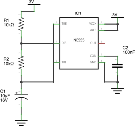
FIGURE 5-13 Connecting C2.
Step 5. Adding the LEDs
Connecting the LEDs and their current-limiting resistors may require a little patience and experimentation to get everything connected. First add one resistor (R3), set its value to be 68Ω, put it in a vertical orientation by rotating it, and then rotate its label back. Once it is right, duplicate it 3 times and spread the resistors out to the right of IC1. Do the same with an LED (in the CORE section of the parts bin). You can set the LED label to hide the color. It would be handy to have the color, but knowing its exact wavelength is unnecessary and clutters the diagram.
Incidentally, if you need to move a group of components, you can drag over an area of the schematic, selecting a number of components, and then drag the whole group. Similarly, you can duplicate a whole group of components by selecting them and then using the CTRL-D keyboard shortcut.
Line up the new components and a duplicate of the 3V supply symbol, as shown in Figure 5-14.
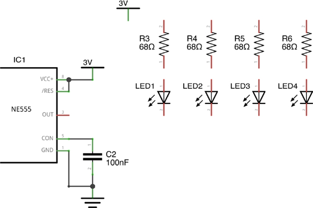
FIGURE 5-14 Lining up resistors and LEDs.
The way to connect a row of components to one net is summarized in Figure 5-15.
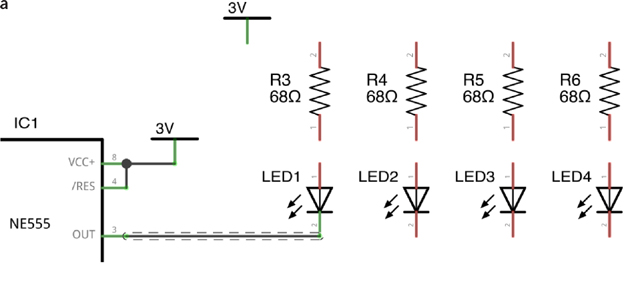
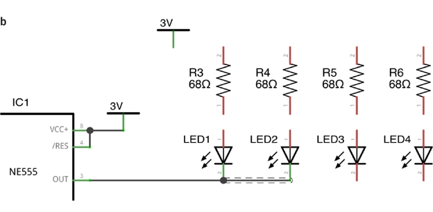
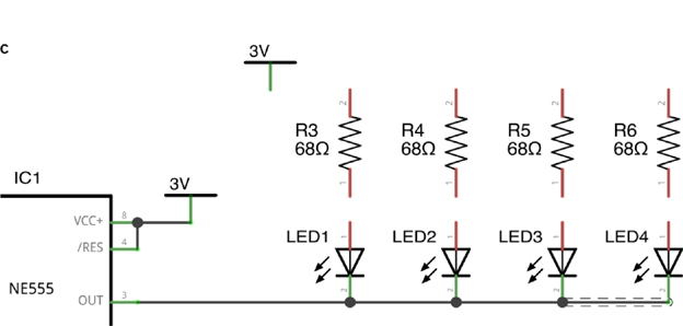
FIGURE 5-15 Connecting a row of components.
Start by connecting pin 3 of IC1 to the bottom of LED1 (Figure 5-15a). Next, drag from the bottom of LED2 back to the bottom of LED1 (Figure 5-15b). If you drag the other way around, then the net will disconnect from the bottom of LED1 and be moved to the bottom of LED2 rather than add a new line to the net. Repeat this process, connecting the bottom of LED3 to LED2 and finally LED4 to LED3 (Figure 5-15c).
Wire up the top of the LEDs to the 3V supply symbol, using the same approach, and join each LED to its resistor. The end result should look like Figure 5-16.
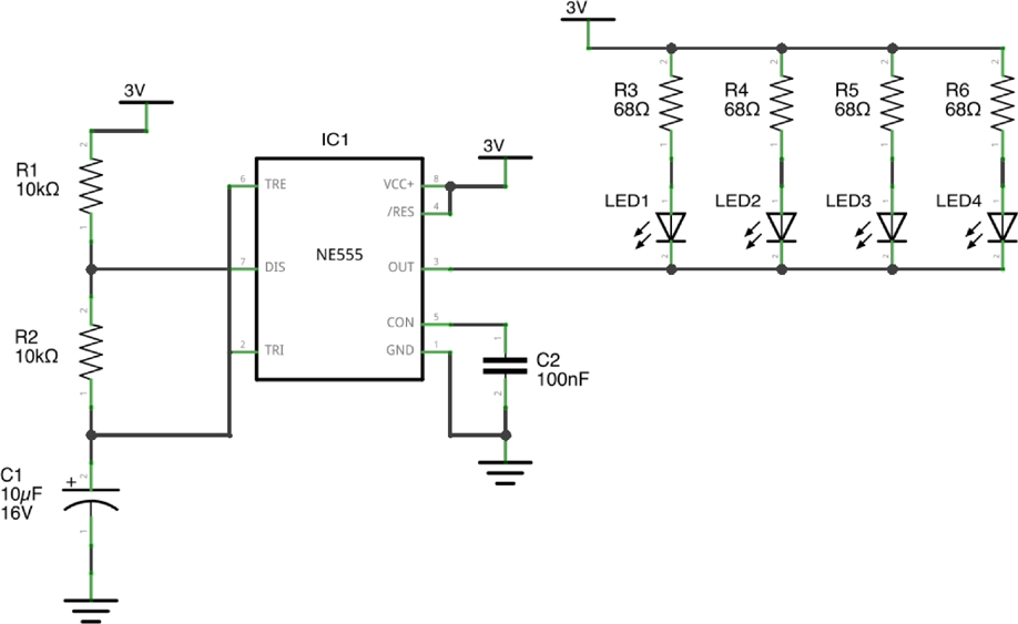
FIGURE 5-16 The LEDs wired up.
Step 6. Adding the Battery and Switch
The schematic is starting to look pretty good now. But it currently has no battery or switch to turn it on and off. It would be good to be able to fit the battery box directly onto the PCB without having extra wires. So, to see what choice of battery holders Fritzing will offer us, type AAA into the Search box of the parts bin. The results are shown in Figure 5-17.
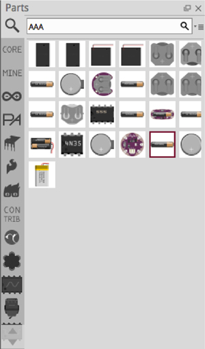
FIGURE 5-17 Finding AAA battery holders.
Some of these are the wrong shape to be AAA battery holders, and others clearly have wires attached (which we are trying to avoid); so add the likely candidates from the results, and you can remove the ones you don’t want later. To see the actual shape of the battery box candidates, switch over to the PCB view. Figure 5-18 shows the best of these.
FIGURE 5-18 The battery box.
The battery box shown in Figure 5-18 is for a single AAA battery, so we will need two of them. The symbol for this battery box rather follows the construction of the battery box itself that has two solder pins for each end of the battery. This is reflected in the symbol, which makes it less clear than the standard battery symbol and is reminiscent of an ancient Egyptian hieroglyph.
Switch back to the Schematic tab, and position the batteries over to the left of the schematic. Also add a switch from the Input section of the CORE parts bin. The switch is labeled Toggle Switch in the parts bin.
Finally connect everything and tidy up the labels, as shown in Figure 5-19. This is the same diagram that you saw in Figure 5-6. I have just repeated it here for convenience.

FIGURE 5-19 The complete schematic.
You will meet this design again in Chapter 6, where it is used as an example for PCB layout.
If you were designing this project as a real product, then you would find the battery box that you wanted to use first and either download (if available) a Fritzing part or create a custom part. You will learn how to make custom parts in Chapter 9.
Advanced Schematic Drawing
Although the bicycle light example covers most aspects of schematic drawing in Fritzing, there are a few techniques that it has not covered that are useful to know.
Net Labels
You have seen how you can use power symbols to reduce the number of lines on the schematic, keeping the spaghetti effect to a minimum. You can also use a similar approach with any nets on the schematic.
Rather than connect two (or more) points on a net with lines, you can add a label to both ends of the net to indicate that they are joined. Figure 5-20 shows a design that uses this approach to connect an Arduino pin to an output circuit to control a motor.
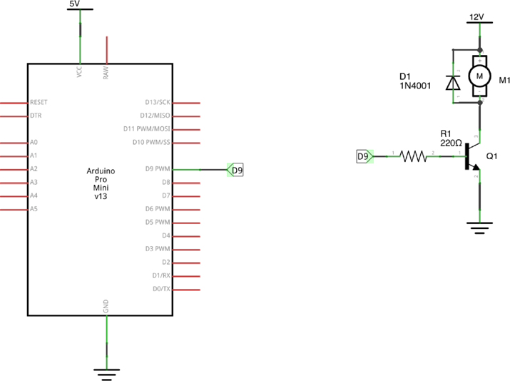
FIGURE 5-20 Using net labels.
The process of creating and linking a net label is summarized in Figure 5-21.
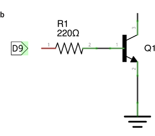
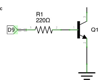
FIGURE 5-21 Creating a net label.
The first step is to add a net label from the Schematic section of the CORE parts bin (Figure 5-21a). Next, use the Inspector to change the label text. The label text does not have to match the net name (Figure 5-21b). Now connect the net label to the net or part terminal that you need to label, using the connection point at the pointy end of the net label (Figure 5-21c). If you connect the label before changing the name, then Fritzing will disconnect the net again when you change the label.
To create the other end of the link, simply duplicate the net label you just created, and then attach it to the other net. You can check that the two nets are actually connected by clicking on one of the component leads connected to one of the labels. For example, click on the left-hand connection to R1 in Figure 5-21. When you do this, both ends of the link will turn yellow for the duration of the click.
If other points in the schematic need connecting to the same net, then just repeat the procedure of duplicating the net label as many times as you need.
Frames
Electronic invention is an iterative process. Your design will get better as you refine the design through successive versions. Keeping track of exactly what version you are looking at will become important. You do not want to accidentally send off an old version of the design for fabrication. So it is important to name your designs carefully.
Including information about the design on the design itself is a good idea. Fritzing includes a special part called a frame for recording information about the design. You will find the frame part in the Schematic section of the CORE parts bin. Figure 5-22 shows the bike light schematic with a frame attached to it.
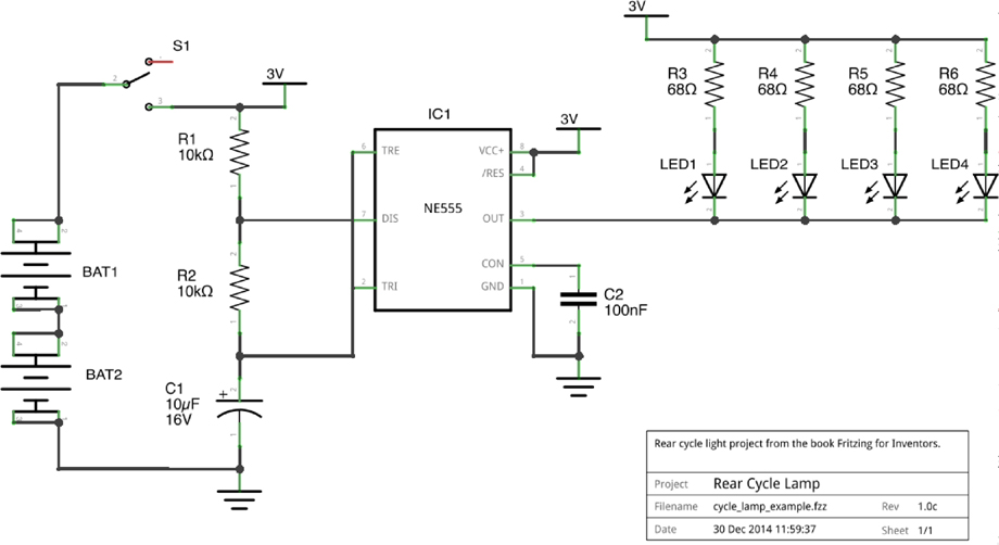
FIGURE 5-22 Adding a frame to a schematic.
It’s conventional to place the frame at the bottom right of the schematic. You can see from Figure 5-22 that the frame contains the Filename and Date that are completed automatically. The description in the topmost area and the project name are set by selecting the frame and then changing the “descr” and “project” attributes in the Inspector.
If you would prefer your frame box to actually have a border that will also enclose the whole schematic, then resize the frame part, dragging its top-left corner up and to the left to enclose the schematic.
The “rev” field is used to record the revision of the design. A common naming convention is to start with version 1.0 and a revision letter of a, b, c, etc. The letter changes are for minor internal changes that only you see. When something changes that other people will see—say, you are getting a new version of the PCB made—then bump the minor version up to 1.1. Changing the big number at the front is reserved for a completely new version of the product.
Datasheets
Datasheets define exactly and reliably how a component behaves. These can be trusted to be correct. For simple components such as individual transistors, they tell you the safe limits for using the device such as the maximum current the transistor can switch before it gets too hot and that kind of thing. For more complex ICs, the datasheet becomes even more useful, as it will often include application notes that include example schematics for using the IC as well as guides for choosing the additional components that the IC may need. These designs are tried and tested, and it is a good idea to base your designs on these schematics.
As an example, take a look at the datasheet for the TLC555 IC. You can find this or any other component by typing the component’s name followed by the word datasheet into your favorite search engine. Here is one link for the TLC555 datasheet from its manufacturer, Texas Instruments: www.ti.com/lit/ds/symlink/tlc555-q1.pdf.
Often you can find out what you need from the summary information at the top of the datasheet. Figure 5-23 shows this for the TCL555.
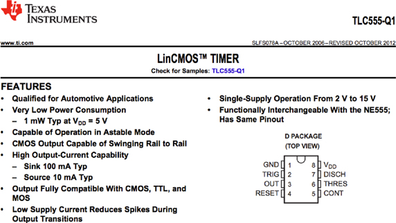
FIGURE 5-23 Datasheet for the LTC555.
On the right-hand side you can see that the operating voltage is 2 to 15V, which is good. Also, on the left-hand side, you can see the words High Output-Current Capability under this, as the datasheet claims a sink current of 100mA. This is more than enough for our four LEDs.
Farther down the datasheet, you will also find a section “Absolute Maximum Ratings.” This tells us that actually, we could get away with sinking 150mA if we really needed to. It is worth reading through the whole datasheet even if you do not understand everything on the datasheet. It will give you an understanding of just what the chip is capable of doing.
Summary
In this chapter, you have learned both how to neaten up a datasheet generated by Fritzing from a breadboard design and how to create a schematic from scratch.
In Chapter 6 you will learn how to create a PCB design for the rear bicycle light project.