
CHAPTER 6
![]()
PCB Layout
In this chapter, you will learn how to design a PCB by using Fritzing. The cycle light project used as an example in Chapter 5 is continued and developed into a full PCB design. Both through-hole and surface-mounted versions of this design are developed.
Printed Circuit Boards
PCBs come with their own set of jargon, and it is worth establishing exactly what we mean by vias, tracks, traces, pads, and layers.
The main focus of the book will be on making double-sided professional-quality boards, either by using the Fritzing integrated PCB service or by e-mailing the design files to a low-cost PCB fabrication service (as low as $10 for 10 boards). The making of PCBs at home is now hardly worthwhile because fabrication services can make PCBs at lower cost and to a better standard than home PCB etching, with all its attendant problems of handling and disposing of toxic chemicals or need for expensive milling machines.
Figure 6-1 shows the anatomy of a two-layer PCB.

FIGURE 6-1 The anatomy of a double-sided PCB.
Refer to Figure 6-1 for the following discussion.
• Pads are where the components are soldered to the PCB. So for through-hole components, each pad will have a hole in the center for the component lead to poke through.
• Tracks or traces are the copper tracks that connect the pads. There can be tracks on both the top and bottom surfaces of the PCB. The traces are insulated by a layer of lacquer called solder mask, over the entire surface of the PCB, except where there are pads to be soldered.
• Vias are small holes through the board that link a bottom and top trace electrically. Traces on the same layer cannot cross, so often when you are laying out a PCB, you need a signal to jump from one layer to another.
• Silk screen refers to any lettering that will appear on the final board. It is common to label components and the outline of where they fit, along with the component’s name, so that when it is time to solder the board, it is easy to see where everything fits.
Cycle Light Example
The main example project in this chapter is the rear cycle light project that was developed in Chapter 5. So if you were following along with that design, open it up again now. You can also load the finished design into Fritzing as the file is called cycle_lamp_example.fzz and is included in the downloads for the book that are available from the author’s website at www.simormonk.org.
Step 1. Spread Out the Parts
When you first switch over to the PCB tab on your design, you will be greeted with something like Figure 6-2.
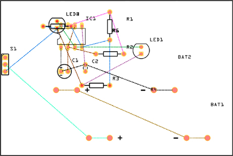
FIGURE 6-2 The initial PCB layout mess.
It even looks as if some of the LEDs and resistors are missing. Actually they are there, but they are just stacked on top of one another. So the first task is to spread out all the components so you can see what’s going on. Figure 6-3 shows the parts spread out, but in no particular order.
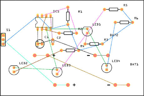
FIGURE 6-3 The components separated on the PCB.
When trying to drag the components apart, you will probably find that you cannot help but hit the dotted lines on the diagram, causing them to turn into orange-colored PCB traces. It’s much too soon to be laying out traces, so when this happens, use the Undo button or CTRL-Z (ALT-Z on a Mac) to undo the trace creation. To help with this problem, you can hover the mouse over the area where you want to click, and a rectangle will appear showing what you are about to click.
Step 2. Place the Parts in Position
In deciding where to position the parts, we want to make their connection as easy as possible, so we need to consider the original schematic. This means we will probably want to have a cluster of components surrounding the integrated circuit (IC).
These are some things to consider when you are deciding where to place components:
• Note the physical constraints that come from the eventual enclosure for the project such as where LEDs and pushbuttons need to be placed.
• Consider the functional grouping of components that are heavily interconnected, such as the IC and its timing components.
• Minimize the messiness of the rat’s nest, and try to reduce the number of times lines cross one another by positioning and rotating the components.
• Make it look nice, and try to keep the design compact but neat.
The LEDs need to be in a row across the middle of the PCB, spanning the whole width, and it makes sense for each of the current-limiting resistors to be near their respective LEDs. Figure 6-4 shows an initial positioning of the components. The components have also been rotated where necessary and labels moved around in just the same way as you did for schematic symbols in Chapter 5.
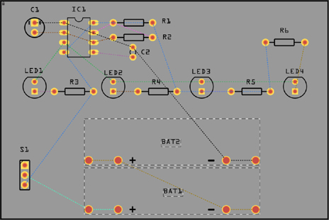
FIGURE 6-4 Initial component positions.
By convention, it is nice to have the IC with the notch at the top of the PCB, so that pin 1 is top left. This is not essential, but can help when you are first getting used to laying out a PCB. Also you will sometimes see a component that would be much easier to connect if it were rotated. For example, the initial orientations of C1 and IC1 are shown in Figure 6-5a. As you can see, the trace lines are crossing. By rotating C1 through 180° (Figure 6-5b), converting the dashed lines into PCB traces becomes trivial. Incidentally, these dashed lines are referred to as the rat’s nest or sometimes air wires.
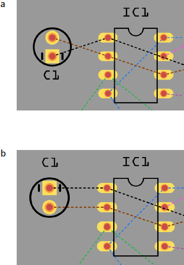
FIGURE 6-5 Rotating components for easier connections.
When you are positioning and rotating the components, use the rat’s nest lines to show you how components are related. Try to minimize the crossing over and long length of the lines.
TIP To stop the PCB as a whole from moving around if you accidentally click on it, you can lock it in position by selecting the gray outline of the PCB away from any components. Right-click and select Lock Part from the menu that pops up. You can always unlock it later if you need to move it.
Step 3. Resize the PCB
Even though in this case the default PCB size is quite good for this design, you could make it a little smaller. The cost of PCB fabrication is usually based on the surface area of the PCB. Also, some PCB fabrication companies have standard dimensions where, at least at the prototyping stage, the PCBs are much cheaper if you limit them to a certain size.
Later in this chapter, you will learn how to use other predefined PCB shapes and even create your own PCB shapes.
Select the PCB as a whole by clicking on the gray background away from any parts, and the Inspector will show the width and height of the PCB. In this case, the width is 84.7mm and the height is 56.4mm. Since 50 and 100mm are common cutoff dimensions, let’s change the height to 50mm and the width to 100mm. That way the battery holders can be side by side, making for a slimmer design.
Select groups of components and shuffle everything to fit within the new PCB border. The switch has moved over to the top right, and the batteries are rotated through 180° so that the positive terminals are to the right. When you have done that, the PCB should look something like Figure 6-6.
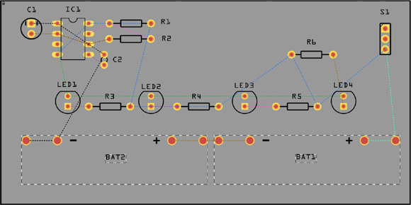
FIGURE 6-6 All the components are in place.
Step 4. Add Fixing Holes
The PCB will eventually need to fit into a plastic enclosure, and this will be easier if we put some holes in the PCB so that we can attach it to the plastic case with screws. Holes are added to the PCB as if they were components, but obviously they have no electrical connections. You will find the hole part in the PCB View section of the CORE parts bin. This is not a big PCB, so two holes should be enough to anchor it securely onto whatever enclosure is used. Drag two holes onto the PCB, either side of the LEDs.
Use the Inspector to change the hole diameter to 3mm. Another property of the hole that you may want to change in the Inspector is the ring thickness. This will provide a copper ring and area clear of copper coated with solder around the hole. This can be used to make electrical connections to a screw through the hole, but in this case there is no need other than I think it looks good.
If this were a real product, you would probably select the screws that you want to use before selecting the hole size.
With the holes added (Figure 6-7), the PCB is now ready for us to start laying down some copper.

FIGURE 6-7 The PCB with mounting holes.
Step 5. Route the Bottom Layer
Fritzing has an Autorouter, which will lay out the traces on your board for you. Try it, if you like, by clicking on the Autoroute button at the bottom of the Fritzing window. If you don’t like the results (and you probably won’t), just click Undo. Personally, I think it is worth taking the time and effort to route a PCB by hand. It acts as an additional check to ensure the design is right as you work through each connection that needs to be made. It’s also fun; it’s like completing a puzzle, getting all the connections made without any of the traces on the same layer crossing over one another.
When laying out a through-hole design like this, I prefer to put much of the wiring into traces on the bottom layer of the PCB. I do not really have a good justification for this, other than that you can usually see the outline of the traces through the lacquer layer and so it just makes the top layer a tiny bit neater.
To control the routing, you use the two controls at the bottom of the Fritzing screen highlighted in Figure 6-8.
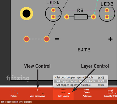
FIGURE 6-8 The view and layer controls.
With lots of traces on the PCB, it can be difficult to see what’s going on. The View control allows you to view the PCB from above or below. Click on it to toggle between the two. Most of the time, you will want to leave this as View from Top. Even when viewing from the top, you will be able to see the traces on the underside of the board. Traces on the top of the board will be shown in yellow and those on the bottom of the board in orange.
The Layer control constrains which layer traces will be drawn on. When you are working on the bottom layer traces, set it to Set Copper Bottom Layer Clickable. This will prevent you from accidentally creating traces on the top layer when you meant to make them on the bottom layer.
Select Set Copper Bottom Layer Clickable and start making the really obvious connections. Remember, the goal is to change all the rat’s nest lines (air wires) into solid copper traces. Use the zoom feature if you are struggling to see where connections are going in a crowded area of the PCB.
Looking at the PCB area around R4 (Figure 6-9a), you can see that there appears to be an air wire connecting both pins of R4. This can’t be right, it just looks that way. Because the air wires have no bend points, they just go straight from one pin to the next. To reveal where the connections really need to go, temporarily move LED2 down a little (Figure 6-9b). You can see that the right-hand pin of R4 is connected to the right-hand pin of R3 (just to the left of LED2), and the line just happens to run through the left-hand pin of R4 because we lined up the components nicely. We will come back to these trickier connections later.
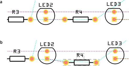
FIGURE 6-9 Untangling air wires.
Now that we are starting to see more complex lines, I changed the background color for the PCB view to be white. Your Fritzing will have a gray background, but you can change this from the View menu if you like.
Set the View control to View from Above and the Layer control to Set Copper Bottom Layer Clickable, and make all the obvious straight-line connections on the bottom surface of the board. Double-clicking on an air wire will turn it into a trace. You can also drag out from one end of the air wire.
You may find that some connections look as if they should route in a straight line, but then Fritzing inserts a bend point for you. This happens around the battery holder pins, as shown in Figure 6-10. If this happens, delete the trace (or CTRL-Z it) and drag it out, again holding down the SHIFT key. You can also remove a bend point by double-clicking on it.
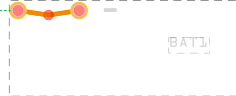
FIGURE 6-10 Unnecessary bend points.
Figure 6-11 shows the PCB with the obvious straight lines all routed. If you make a mistake, then CTRL-Z will undo the last action. You can also select a trace and then press the DELETE key or select Delete from the right-click menu. This will delete just the trace, not the underlying need for a connection. In other words, this will not affect the schematic. Do not be tempted to use the Delete Rat’s Nest option as this will change the circuit. If you do this and flip over to the Schematic view, you will find that a line has vanished.
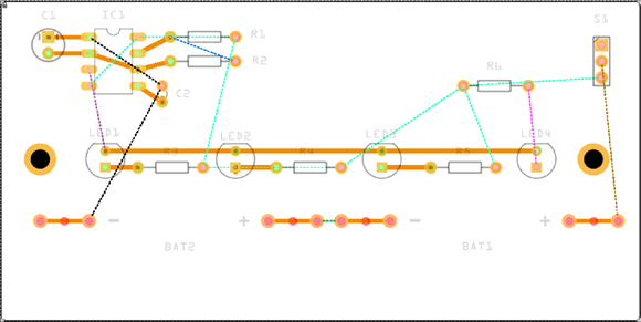
FIGURE 6-11 The “low-hanging fruit” traces on the bottom layer.
So far, so good. Staying with the bottom layer, make the trace between pin 3 of IC1 and the top connection of LED1. This needs to come out and away from pin 4 of IC1. Let’s keep the traces on the PCB more or less vertical or horizontal for the sake of neatness.
Start at the IC1 pin 3 end of the connection because this does not have other connections branching off it as the LED1 end does. Drag from the air wire near the pin rather than from the pin itself. Start to drag out to the left from IC1 pin 3, and a bend will appear in the air wire (Figure 6-12a). This is great, because now we can see exactly the intended destination of the trace. Release the mouse button and a trace will be drawn (Figure 6-12b). This is okay, but let’s neaten it up by adding another bend point and then moving both bend points. Figure 6-12c shows the final result of making this trace.
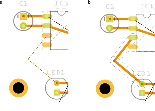
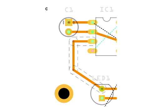
FIGURE 6-12 Connecting with bend points.
I have gone with an angled trace segment for the last bit of the connection to LED1 to keep the trace well away from the hole to the left of LED1.
Another tricky routing problem arises when you want to route the traces one way, but the rat’s nest air wires are steering you in another direction. The air wires always take the shortest-distance route from one connection to another. For example, in Figure 6-13a, two air wires go from the right-hand terminal of R4 to the left-hand terminal of R6 and then the right-hand terminal of R5. In this case, it would be a whole lot easier to route from R4 to R5 and then connect the right-hand pin of R6 to the bottom pin of the switch.
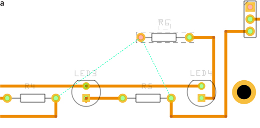
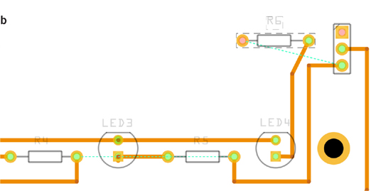
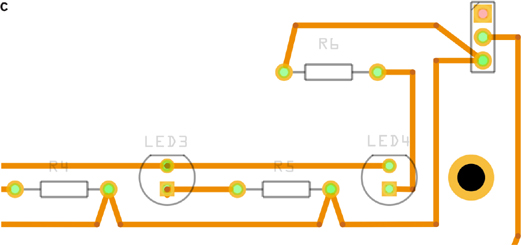
FIGURE 6-13 Changing the rat’s nest routing.
Making these connections in the way that you want can take a bit of trial and error. One way to force this route, temporarily drag R6 up and to the right. This will cause the rat’s nest to rearrange itself as we would like (see Figure 6-13b). Finally, we can wire the air wires and then move R6 back and rearrange the bend points to get the result shown in Figure 6-13c.
You can also route away from air wires, if you click on one of the alternative connection points that will be highlighted in yellow as you start to drag out an air wire.
Repeat this process for all the other connections that can be made on the bottom surface of the PCB, without crossing any of the existing traces. Use Figure 6-14 as a guide. Note that when you come to route the right-hand connection of R1, Fritzing is suggesting that we route this to the right-hand connection of R3. We can’t do this without crossing a trace, so it would be much easier to connect it to the left-hand pin of R6. To make the air wire reroute, temporarily drag R6 over toward R1, make the trace, and then drag R6 back to its original position.
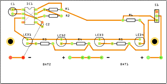
FIGURE 6-14 All the bottom traces routed.
There is no need to worry about traces crossing over the component labels, as these will be printed on top of the traces.
If you have arrived at the stage shown in Figure 6-14, there are only three air wires left to be routed.
Step 6. Route the Top Connection
Looking carefully at the connections that remain, you can see that the top pin of C2, pin 1 of IC1, and the negative battery connection are all ground connections. We will handle these, using something called a ground fill, in the next step. This just leaves one connection to be made on the top surface of the board, between pins 4 and 8 of IC1. To make this connection, select the option Set Copper Top Layer Clickable on the Layer control, and then join the pins on IC1 as shown in Figure 6-15.
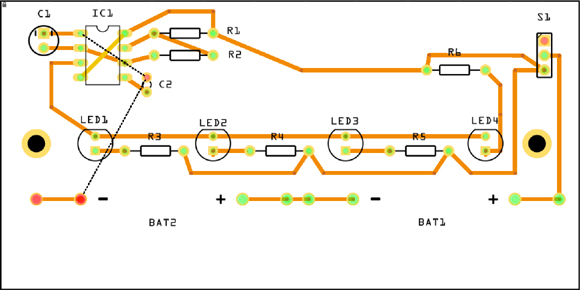
FIGURE 6-15 Routing the top layer.
Note that the trace on the top layer is shown in a mustard yellow color rather than the more orange color of the bottom layer traces. It does not matter that the trace between pins 2 and 6 of IC1 crosses the trace between pins 4 and 8 because one is on the top layer and the other is on the bottom.
Step 7. Add a Ground Fill
It is a common practice in PCB design to use a ground fill (sometimes called a ground plane). This ground fill is optional and can be on one or both of the copper layers. A ground fill makes all the layer one big area of copper connected to the ground net, apart from channels in the ground fill for traces that are on that layer, but not connected to ground.
You will use this ground fill as a way of connecting the three remaining unrouted pins.
Set the View control to be View from Above and the Layer tool to Bottom Layer. Now from the Routing menu select the options Ground Fill and Ground Fill Bottom. The board should now look like Figure 6-16.
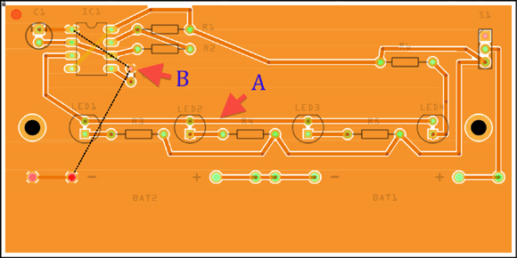
FIGURE 6-16 Adding a ground fill to the bottom layer.
There are a couple of things to note in Figure 6-16. First, the non-ground traces are now in a channel, with a copper-free narrow gap on each side of the traces (A). Second, if you look closely at the negative battery connection, the top pin of C2, and pin 1 of IC1, you can see that they all have little traces from the ground fill to the pad (marked with B). Figure 6-17 shows a close-up of this for the battery terminal.

FIGURE 6-17 A pad connected to the ground fill.
There is an interesting reason why the ground fill only connects to the pad on each side, rather than simply covering the pad. The reason is that when you solder a pad, it has to get hot; and if the pad is effectively the whole ground plane, then it is much harder to get the part of the pad hot that needs to be hot, as a lot of heat is carried away into the surrounding copper.
The other thing that you will notice from Figure 6-16 is that the air wires for the ground connections are still there despite the connections having been made by the ground fill. This is a “feature” of the version of Fritzing used here (Version 0.8.7), and this may well have been fixed in your version. There are two work-arounds for this:
• If you are sure that the connections are actually made by the ground-fill layer, then you can simply hide those few remaining air wires from the View menu by deselecting the Rat’s nest Layer.
• If you explicitly connect up the remaining air wires as traces, before adding the ground fill, this will also remove the air wires.
At this point, it is a good idea to look carefully at the ground fill and make sure that there is some route between the pins relying on it. The only pin you might have doubts about is the top of C2, as the ground fill here looks a bit like an island. However, there is a connection, because the ground fill copper seeps between the pins of IC2, so all parts of the ground fill are connected.
Step 8. Add Text and a Logo
The PCB is starting to look pretty professional. As a final touch, add some text to identify the PCB version and for good measure a logo graphic.
To add text, just drag a Text part from the PCB View section of the CORE parts bin onto the PCB. You can then edit the text in the Inspector. If you want to add an icon too, then drag a Silkscreen Image from the parts bin. There are a few different icons to select from in the Inspector. I have chosen the Open Hardware logo, to show that this design is Open Source. The end result of this is shown in Figure 6-18.
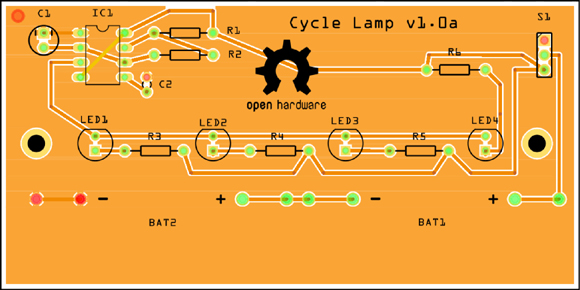
FIGURE 6-18 The PCB design with text and logo.
The rat’s nest has vanished because, having assured myself that they have actually been routed, I have deselected Rat’s Nest Layer from the View menu.
Step 9. Design Rule Check
On a simple design like this, it is fairly easy to manually check the design for traces crossing on the same layer, running too close to pads, etc. However, it is always worth running the Design Rule Checker (DRC), which will automatically check for these things. You can run this from the Routing menu. Once it has run, if all is well, you will get a message that says: “Your sketch is ready for production: there are no connectors or traces that overlap or are too close together.”
Hurray, your PCB layout is good to go. In Chapter 7, you will learn how to go about having real PCBs made from your design as well as how to solder components to them. But before that, there are quite a lot of details that we skipped over in this example that I want to catch up on.
Advanced PCB Layout
In using the cycle lamp PCB example, there are a few features of Fritzing that we haven’t needed to use and some aspects that we have only touched on. In this section we will fill those gaps.
Moving Traces Between Layers
If you draw a trace on the bottom layer and then decide it would be better on the top, you can right-click on the trace and select the option Move to Top Layer. A similar option will appear in the menu when you have a trace on the top layer that you want to move to the bottom.
You can also change the layer of a trace by selecting it and then using the Inspector (Figure 6-19). The Inspector also allows a number of other things about the trace to be changed.

FIGURE 6-19 Selecting a trace layer from the Inspector.
Changing Trace Widths
The wider a trace, the more current it can carry without overheating. By default, Fritzing uses a trace width of 24 mils. The unit mil is often confused with mm. These are not the same. One mil is 1/1000 inches. In modern PCB design, 24 mils is actually a medium width. Many PCB manufacturers will allow you to use traces down to 6 mils. If there is plenty of room on the PCB, then 24 mils is a good width to use for most purposes.
In a later section of this chapter, you will see how for surface-mounted components, 24 mils can be a bit too wide, and you will need to use something thinner.
Where you have a higher current part of the PCB design, you should use thicker traces.
Table 6-1 provides a rough guide to the current-carrying capabilities of various trace widths. These figures are based on a maximum allowable increase in temperature of the trace of 10°C at an ambient temperature of 25°C and a 100mm trace length.
TABLE 6-1 Current-Carrying Capabilities of Various Track Widths
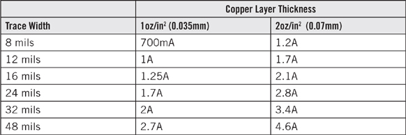
The data for Table 6-1 are derived from the useful online calculator at http://circuitcalculator.com/wordpress/2006/01/31/pcb-trace-width-calculator/.
For historical reasons, the most common thickness of copper on PCBs is 1oz/ft2. That is 1oz of copper spread over 1ft2. In other words, it is pretty thin (about 0.035mm). PCB manufacturers will often offer a thickness of 2oz/ft2 (0.07mm). Just stick to 1oz/ft2 unless you have a good reason to do otherwise.
As you can see from Table 6-1, even a very thin 8mil trace can carry a fairly sizable current before getting warm enough for any long-term damage to the PCB to occur.
Placing Components on the Bottom Layer
At present, all the components for the cycle lamp are mounted on the top surface of the PCB. The board could be made a little smaller if the battery holders were mounted on the underside of the board. The obvious advantage of putting components on both sides of the board is that it saves space and allows you to make a smaller PCB. The disadvantage is that it may increase manufacturing costs.
Switching a component itself from the top layer to the bottom layer is quite straightforward. You select the components (for example, BAT2) and then in the Inspector select Bottom from the PCB Layer drop-down list. Do this for both BAT1 and BAT2, and the resulting layout will look like Figure 6-20a. Notice how when you look from above, the labels for BAT1 and BAT2 are in mirror image. It is as if we are looking through the top surface of the board.

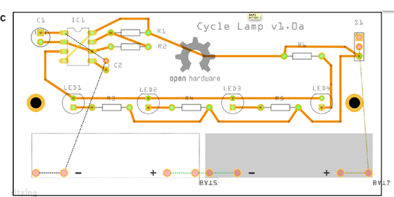
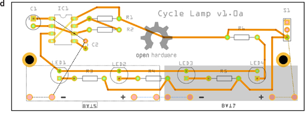
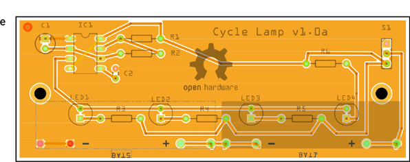
FIGURE 6-20 Moving the battery holders to the underside of the PCB.
You can see in Figure 6-20a that as you might expect, this has messed up the routing of traces considerably. So remove the ground fill and delete all the wires around the battery holders so that we can see what’s going on (Figure 6-20b).
In Figure 6-20b, most of the layout mess stems from the fact that now the battery holders are on the other side of the board—their positive terminals are now to the left of the board rather than to the right. In moving the battery holders to the bottom layer, they have been flipped from left to right. To fix this, we can rotate both battery holders by 180° (Figure 6-20c). Thus the body of the battery holders is toward the center of the PCB, allowing us to make the PCB a bit smaller, as there is now an empty area at the bottom.
Now move the mounting holes and the battery boxes up a bit and resize the PCB (Figure 6-20d). In moving the left-hand mounting hole, the trace from pin 3 of IC1 also had to be moved a little. The labels for BAT1 and BAT2 need to be moved as well.
Route the remaining air wires and reapply the ground fill. The final PCB is shown in Figure 6-20e.
Vias
In the cycle lamp example, there are not so many parts, and they are well spaced out, so routing is pretty easy. Also since it is a though-hole design, there are naturally lots of places where a component lead can be used to connect a trace on one side of the board to the other.
In many PCB layouts, especially on surface-mounted designs, you need to route an air wire as a trace that starts on one layer and then swaps to another layer, often returning to the first layer after it has crossed over some traces that were in the way of a direct connection.
To connect between the layers like this, you need to use a via. Basically a via is a through-hole component lead, but without the component itself.
As an example, let’s change the routing on the cycle lamp project to deliberately introduce a via to connect the right-hand side of R5 to the left-hand side of R6, without having to visit S1 on the way (Figure 6-21a shows the old and new routes).

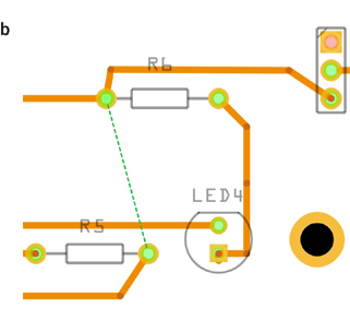
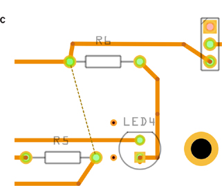
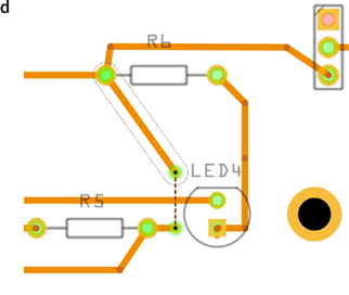
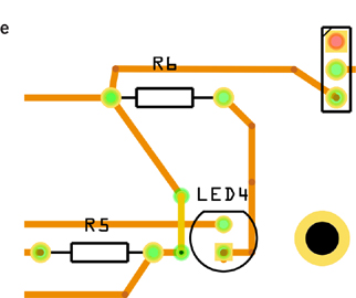
FIGURE 6-21 Using a via.
To reroute this part of the design to use a via, first you need to remove the ground fill by using the Remove Copper Fill option on the Ground Fill submenu of the Routing menu. You will add the ground fill back again later. Also delete the traces that you are going to change by right-clicking on the old route and selecting the Delete Wire option. The result of this is shown in Figure 6-21b. Interestingly, the air wire now shows a direct connection in the route that we want to take. You cannot simply drag a trace on the bottom layer from the right-hand lead of R5 to the left-hand lead of R6, because that would cross the horizontal track between LED3 and LED4. In this case we could route a track on the top layer, but since we want to illustrate the use of vias, we will ignore that option and instead add two vias from the PCB section of the CORE parts bin (Figure 6-21c). Position one via between the right-hand lead of R5 and the bottom lead of LED4. Add the second via vertically above the first via, but on the other side of the horizontal line that is in the way. We are going to use the pair of vias as a kind of bridge over the horizontal track.
Set the Layer control to Bottom Layer and drag a trace from the bottom via to the right-hand connection of R5. Then drag a trace from the top via to the left-hand connection of R6 (Figure 6-21d). Finally, flip the Layer control to the top layer, and drag a trace on the top layer from one via to the other. The final result is shown in Figure 6-21e. You can then reapply the ground fill.
You will meet vias again when we make a surface-mounted version of the cycle lamp.
Icons Revisited
Fritzing is supplied with a few ready-made icons, such as the OSH logo, which you can add to your PCBs. You can also add your own custom logo to the PCB. The first step in adding your own logo is to create an image file.
The silk screen layer of the PCB is usually made up of white onto the green solder mask layer of the PCB. There are no shades of gray. So any image that you add will be reduced to a bit depth of 1. For best results you should design the image with this in mind. Once the image is added, you will be able to resize it. For best results, use a SVG vector image, although Fritzing will also accept a PGN format image.
There are many software packages available for creating images like this, and the open-source software Inkscape will do just fine. Once you have created a suitable image in Inkscape, you will need to adjust the document size to fit the image. You will find the option to do this in Document Properties in Inkscape (see Figure 6-22). Now, add an Image to the PCB and click on the Load Image File button to select the image file. Resize and move it, and your icon will be on the board, as shown in Figure 6-23.
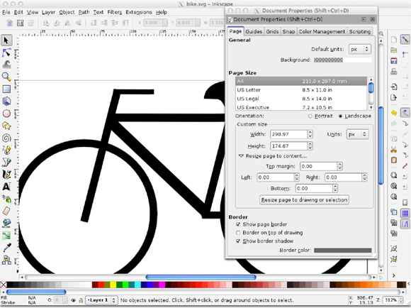
FIGURE 6-22 Adjusting the document size in Inkscape.
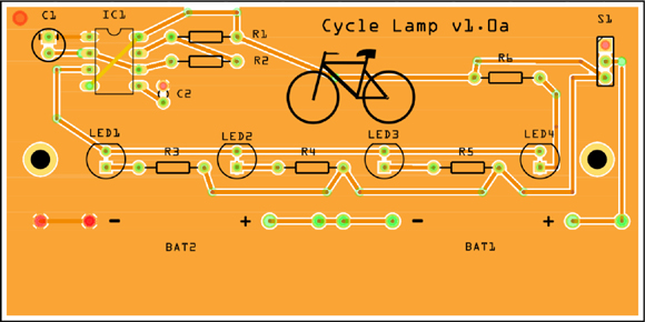
FIGURE 6-23 A custom icon on the PCB.
Fills Revisited
In the cycle lamp project, we applied a ground fill to only the bottom layer. You can, in fact, add fills to both layers and specify whether they should be connected to GND. These options are available from the Routing menu (Figure 6-24).

FIGURE 6-24 Fill options.
They layers available for filling will change depending on what you have selected with the Layers tool at the bottom of the Fritzing window. If you select an option that is just Copper Fill rather than Ground Fill, then the layer will be filled, but not connected to the ground net.
Fritzing will automatically look for nets that are named GND or Ground and upon finding them will connect them to a ground fill automatically. You can confirm this by checking that a component pin that you know to be connected to GND is connected to the fill.
Board Shapes
The cycle lamp PCB is a sharp-cornered rectangle. That’s just fine, it does the job, but it would look a bit nicer if the corners were rounded. It’s a little thing, but does add a nice touch to the board.
There are quite a few specialized shapes built into Fritzing as well as options for Rectangle and Round Rect. You can access these by selecting the board itself, by clicking well away from any parts; then in the Selector, click on the Shape drop-down list. Select Round Rect and the cycle light board will get rounded edges. The ground fill will, however, still be rectangular, so remove the ground fill and then add it again. Now the board should look like Figure 6-25.

FIGURE 6-25 Adding rounded edges to the PCB.
Fritzing also allows you to create boards of any shape you like by supplying it with an SVG image file. This image is a bit special in that it must have two layers. One layer is for the board outline itself, and one is for the available silkscreen layer. Both layers will normally be of the same shape and on top of each other. The shape on the board layer needs a solid fill color (by convention green) and no stroke. The silkscreen layer must have no fill and a white stroke of 0.2mm, which makes it a little tricky to see.
To create such a shape in Inkscape, perform the following steps:
1. Create a layer and name it “board.”
2. Draw your shape at the size that you want on the board level.
3. Set the shape’s fill color to green, and set its outline to have no stroke.
4. In the Layers area (bottom right of Figure 6-26), select the board layer; then right-click on it and select the option Duplicate Current Layer.
5. Rename the current layer silkscreen.
6. Select the duplicated shape on the silkscreen layer, and set its stroke to 0.2mm white. Next, set its fill to None.
7. Save the file. Select the Save As… menu option, and in the file dialog select the file type of Plain SVG (*.svg) before saving the file.
8. Fix the saved file in a text editor.
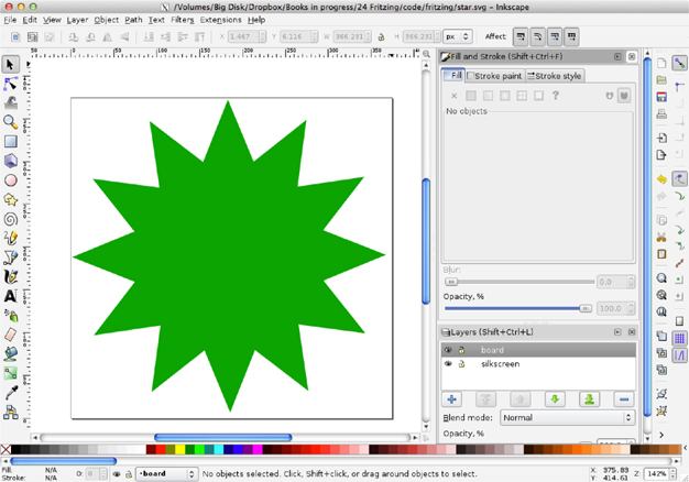
FIGURE 6-26 Creating a custom PCB shape in Inkscape.
Step 8 is necessary, because unfortunately when Inkscape saves a layer, it does not transfer the name attribute that you specified for the layer (that is, “board” or “silkscreen”). So open the image file in a text editor, and search for the first “g” tag, something like the following example:

Replace the value of the id attribute to be “silkscreen,” as shown below:

A little farther down the file there should be another “g” tag. Change the id of this tag to “board” and then save the file.
Now that you have a file in the correct format, you can apply that shape to any PCB, by selecting the PCB in the PCB tab and then clicking on the Load Image File option. You will notice that a dialog pops up, asking you to check the Gerber production files before you rely on this feature working. Checking the Gerber files in a Gerber viewer is always a good idea until you become really confident with Fritzing; this is discussed in Chapter 7. An example PCB using a starting shape is shown in Figure 6-27. You can find both the image file (star.svg) and the Fritzing file (ch_06_PCB_Shape.fzz) in the downloads available for this book.
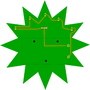
FIGURE 6-27 A star-shaped PCB.
SMD PCBs
Surface-mount devices (SMDs) cost less and are smaller than the through-hole components we used to develop the cycle light project. We could actually take the design and modify it to use mostly surface-mount components.
SMD Components
Not all the components we used in the project have surface-mount counterparts. Take, for example, the battery holders. Also some of the components might be better as through-hole. The LEDs will have bigger, better lenses as 5mm through-hole than tiny surface-mount devices. However, for the sake of illustrating a surface-mount layout, let’s replace everything we can with SMDs.
Resistors
Starting with the resistors, we have used ¼W resistors. This is an indication of the power the resistor can handle, and ¼W is fine. Before choosing SMD equivalents of the resistors, we need to know the power rating we should aim for with the resistors. The power is the current flowing through the resistor, multiplied by the voltage across it. In Chapter 5, we selected a 68Ω resistor that would give us a current of 20mA. The voltage of the batteries is 3V, and 1.7V of that will be across the LED, leaving 3 – 1.8 = 1.3V across the resistor. So the power will be 1.3V × 20mA = 26mW. If you want to know the theory, then take a look at http://en.wikipedia.org/wiki/LED_circuit. There are also online calculators that will do the math for you, such as this one: http://led.linear1.org/1led.wiz.
Common SMD resistor values are listed in Table 6-2.
TABLE 6-2 Resistor Packages and Power Ratings
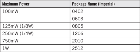
The package names represent the resistors’ dimension in tens of mils. So the package 0402 is 40 mils by 20 mils.
For our needs, 0402 resistors would be fine, but if you’ve ever tried to solder a 0402 resistor by hand, you might prefer to use the much larger 0805.
Capacitors
Small-value capacitors such as the 100nF capacitor are generally available in the same sizes as the resistor sizes listed in Table 6-2; however, electrolytic capacitors use a different sizing scheme—several schemes in fact. One popular size range is the Panasonic range that is designated by a letter, e.g., Panasonic A, B, C, D, or E. When selecting the right package, you will probably need to check out component suppliers, find a capacitor of the right capacitance and voltage rating, and look at its datasheet to find its package size.
Semiconductors
Transistors and ICs also have a variety of package sizes. For example, a 555 timer is generally available as a through-hole DIL-8 (8-pin dual-in-line) package or a surface-mount SO8 (Small Outline 8-pin) package.
Transistors are also available in different SMD packages of different sizes. Generally, the bigger packages for transistors can handle larger currents. The most common SMD transistor size for small transistors is SOT-23.
Making a Surface-Mount Version
You will find an SMD version of the project in the file cycle_lamp_example_smd.fzz with the other downloads for this book. Unfortunately, the version of the 555 timer part that I selected (because it had meaningful names for its pins) only had a through-hole DIL package, whereas another of the 555 alternatives did have an SMD package. So the schematic switches to that version of the 555 chip. Ideally, you would make a copy of the well-labeled 555 part and then edit that part to add the SMD package; but we do not discuss creating and editing parts until Chapter 9.
Replace the Part Packages
Figure 6-28 shows the through-hole design, with the ground fill removed and all the traces unrouted. A quick way of removing all the traces from the design is to use the Select All Traces option on the Routing menu and then hit the DELETE key.
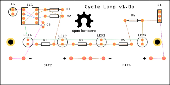
FIGURE 6-28 The through-hole design stripped back.
The next step is to click on each of the components in turn and then select an SMD package. The result is shown in Figure 6-29.
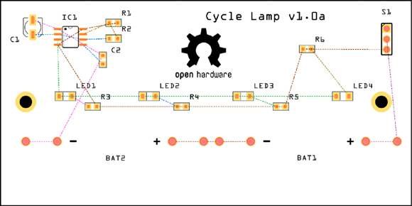
FIGURE 6-29 Through-hole parts replaced with SMDs.
Change the C1 package to “0405 SMD.” Notice that after you add it, the air wires to IC1 cross over; so rotate it through 180° to make it easier to connect. Similarly, when IC1 is replaced with an SO8 package, it will need to be rotated 90° clockwise.
Change all the resistors and C2 to an 0805 package, rotating where necessary. Change the LEDs to the largest possible size of 1206. The PCB layout should now look something like Figure 6-30. There is now a lot of space around all the components, and we could easily reduce the size of the PCB. In this case, the lamp needs to be reasonably big so that it can be seen easily. Other board designs usually need to be as compact as possible.
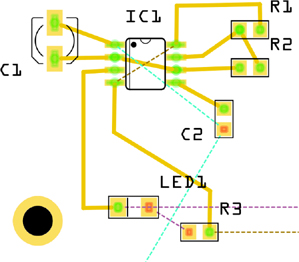
FIGURE 6-30 Routing around IC1.
Reroute the Design
When you are routing with SMDs, it is always best to start on the top layer. Since they do not have leads passing through the PCB, there is no connection to the bottom layer unless you add vias. Also if you look at the pins of IC1, you can see that our default trace size of 24 mils is actually a bit wider than the pad for the pins. So let’s route the traces with a track width of 16 mils around IC1 and 24 mils where the pads are big.
The default setting for the grid is 0.05in (50 mils). SMD connections have closer spacings than their through-hole counterparts, so change the grid size to 0.01in (10 mils) by using the Set Grid Size option on the View menu.
Route all the traces around IC1 and set the trace width to 16 mils for each trace. Leave the unrouted connections that are to be connected to ground, as you are going to have ground fills top and bottom in this design. When the area around IC2 is complete, it should look like Figure 6-30.
After IC1 is routed, do as much of the routing as possible on the top layer, as that is where the SMD pads are. You can do all this routing at the default 24 mils. The connection between pins 4 and 8 of IC1 can be taken care of with a long trace from the right-hand connection of R1 round to the left connection of R6. Follow the trace through S1, R5, R4, and R3 to see how that connection works. In this circuit it will not matter that we have such a long connection. But in some designs, especially in audio amplifier or radio-frequency designs, you need to keep traces as short as possible. In that case, you would route the connection between pins 4 and 8 of IC1 directly, using vias.
The end result of this is shown in Figure 6-31.
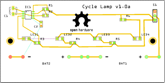
FIGURE 6-31 Top layer routing.
The only traces that remain to be routed are the ground connections that will be taken care of by the ground fills and the connection between the left-hand pad of LED1 and the left-hand pad of LED2. Route the connection between LED1 and LED2, using a pair of vias, as shown in Figure 6-32. At this point, add back the ground fills on both layers to complete the layout. To do this, you will need to first set the Layers control to allow connections on both layers.
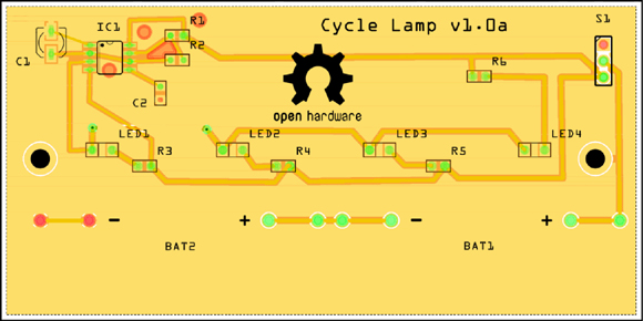
FIGURE 6-32 The completed surface-mount layout.
Summary
In Chapter 7 you will learn how to take your PCB layout, turn it into a real PCB, and solder components onto it.